EP3554823B1 - A bi-layer nanoparticle adhesion film - Google Patents
A bi-layer nanoparticle adhesion film Download PDFInfo
- Publication number
- EP3554823B1 EP3554823B1 EP17880180.9A EP17880180A EP3554823B1 EP 3554823 B1 EP3554823 B1 EP 3554823B1 EP 17880180 A EP17880180 A EP 17880180A EP 3554823 B1 EP3554823 B1 EP 3554823B1
- Authority
- EP
- European Patent Office
- Prior art keywords
- nanoparticles
- substrate
- layer
- group including
- nanoparticle
- Prior art date
- Legal status (The legal status is an assumption and is not a legal conclusion. Google has not performed a legal analysis and makes no representation as to the accuracy of the status listed.)
- Active
Links
Images


Classifications
-
- H—ELECTRICITY
- H10—SEMICONDUCTOR DEVICES; ELECTRIC SOLID-STATE DEVICES NOT OTHERWISE PROVIDED FOR
- H10W—GENERIC PACKAGES, INTERCONNECTIONS, CONNECTORS OR OTHER CONSTRUCTIONAL DETAILS OF DEVICES COVERED BY CLASS H10
- H10W70/00—Package substrates; Interposers; Redistribution layers [RDL]
- H10W70/40—Leadframes
- H10W70/456—Materials
- H10W70/458—Materials of insulating layers on leadframes
-
- B—PERFORMING OPERATIONS; TRANSPORTING
- B32—LAYERED PRODUCTS
- B32B—LAYERED PRODUCTS, i.e. PRODUCTS BUILT-UP OF STRATA OF FLAT OR NON-FLAT, e.g. CELLULAR OR HONEYCOMB, FORM
- B32B15/00—Layered products comprising a layer of metal
- B32B15/04—Layered products comprising a layer of metal comprising metal as the main or only constituent of a layer, which is next to another layer of the same or of a different material
- B32B15/08—Layered products comprising a layer of metal comprising metal as the main or only constituent of a layer, which is next to another layer of the same or of a different material of synthetic resin
- B32B15/092—Layered products comprising a layer of metal comprising metal as the main or only constituent of a layer, which is next to another layer of the same or of a different material of synthetic resin comprising epoxy resins
-
- B—PERFORMING OPERATIONS; TRANSPORTING
- B32—LAYERED PRODUCTS
- B32B—LAYERED PRODUCTS, i.e. PRODUCTS BUILT-UP OF STRATA OF FLAT OR NON-FLAT, e.g. CELLULAR OR HONEYCOMB, FORM
- B32B15/00—Layered products comprising a layer of metal
- B32B15/18—Layered products comprising a layer of metal comprising iron or steel
-
- B—PERFORMING OPERATIONS; TRANSPORTING
- B32—LAYERED PRODUCTS
- B32B—LAYERED PRODUCTS, i.e. PRODUCTS BUILT-UP OF STRATA OF FLAT OR NON-FLAT, e.g. CELLULAR OR HONEYCOMB, FORM
- B32B15/00—Layered products comprising a layer of metal
- B32B15/20—Layered products comprising a layer of metal comprising aluminium or copper
-
- B—PERFORMING OPERATIONS; TRANSPORTING
- B32—LAYERED PRODUCTS
- B32B—LAYERED PRODUCTS, i.e. PRODUCTS BUILT-UP OF STRATA OF FLAT OR NON-FLAT, e.g. CELLULAR OR HONEYCOMB, FORM
- B32B27/00—Layered products comprising a layer of synthetic resin
- B32B27/38—Layered products comprising a layer of synthetic resin comprising epoxy resins
-
- B—PERFORMING OPERATIONS; TRANSPORTING
- B32—LAYERED PRODUCTS
- B32B—LAYERED PRODUCTS, i.e. PRODUCTS BUILT-UP OF STRATA OF FLAT OR NON-FLAT, e.g. CELLULAR OR HONEYCOMB, FORM
- B32B3/00—Layered products comprising a layer with external or internal discontinuities or unevennesses, or a layer of non-planar shape; Layered products comprising a layer having particular features of form
- B32B3/02—Layered products comprising a layer with external or internal discontinuities or unevennesses, or a layer of non-planar shape; Layered products comprising a layer having particular features of form characterised by features of form at particular places, e.g. in edge regions
- B32B3/08—Layered products comprising a layer with external or internal discontinuities or unevennesses, or a layer of non-planar shape; Layered products comprising a layer having particular features of form characterised by features of form at particular places, e.g. in edge regions characterised by added members at particular parts
-
- B—PERFORMING OPERATIONS; TRANSPORTING
- B32—LAYERED PRODUCTS
- B32B—LAYERED PRODUCTS, i.e. PRODUCTS BUILT-UP OF STRATA OF FLAT OR NON-FLAT, e.g. CELLULAR OR HONEYCOMB, FORM
- B32B7/00—Layered products characterised by the relation between layers; Layered products characterised by the relative orientation of features between layers, or by the relative values of a measurable parameter between layers, i.e. products comprising layers having different physical, chemical or physicochemical properties; Layered products characterised by the interconnection of layers
- B32B7/04—Interconnection of layers
- B32B7/10—Interconnection of layers at least one layer having inter-reactive properties
-
- B—PERFORMING OPERATIONS; TRANSPORTING
- B32—LAYERED PRODUCTS
- B32B—LAYERED PRODUCTS, i.e. PRODUCTS BUILT-UP OF STRATA OF FLAT OR NON-FLAT, e.g. CELLULAR OR HONEYCOMB, FORM
- B32B7/00—Layered products characterised by the relation between layers; Layered products characterised by the relative orientation of features between layers, or by the relative values of a measurable parameter between layers, i.e. products comprising layers having different physical, chemical or physicochemical properties; Layered products characterised by the interconnection of layers
- B32B7/04—Interconnection of layers
- B32B7/12—Interconnection of layers using interposed adhesives or interposed materials with bonding properties
-
- H—ELECTRICITY
- H10—SEMICONDUCTOR DEVICES; ELECTRIC SOLID-STATE DEVICES NOT OTHERWISE PROVIDED FOR
- H10W—GENERIC PACKAGES, INTERCONNECTIONS, CONNECTORS OR OTHER CONSTRUCTIONAL DETAILS OF DEVICES COVERED BY CLASS H10
- H10W70/00—Package substrates; Interposers; Redistribution layers [RDL]
- H10W70/01—Manufacture or treatment
- H10W70/04—Manufacture or treatment of leadframes
-
- H—ELECTRICITY
- H10—SEMICONDUCTOR DEVICES; ELECTRIC SOLID-STATE DEVICES NOT OTHERWISE PROVIDED FOR
- H10W—GENERIC PACKAGES, INTERCONNECTIONS, CONNECTORS OR OTHER CONSTRUCTIONAL DETAILS OF DEVICES COVERED BY CLASS H10
- H10W70/00—Package substrates; Interposers; Redistribution layers [RDL]
- H10W70/40—Leadframes
- H10W70/456—Materials
- H10W70/457—Materials of metallic layers on leadframes
-
- H—ELECTRICITY
- H10—SEMICONDUCTOR DEVICES; ELECTRIC SOLID-STATE DEVICES NOT OTHERWISE PROVIDED FOR
- H10W—GENERIC PACKAGES, INTERCONNECTIONS, CONNECTORS OR OTHER CONSTRUCTIONAL DETAILS OF DEVICES COVERED BY CLASS H10
- H10W70/00—Package substrates; Interposers; Redistribution layers [RDL]
- H10W70/60—Insulating or insulated package substrates; Interposers; Redistribution layers
- H10W70/67—Insulating or insulated package substrates; Interposers; Redistribution layers characterised by their insulating layers or insulating parts
- H10W70/68—Shapes or dispositions thereof
- H10W70/6875—Shapes or dispositions thereof being on a metallic substrate, e.g. insulated metal substrates [IMS]
-
- H—ELECTRICITY
- H10—SEMICONDUCTOR DEVICES; ELECTRIC SOLID-STATE DEVICES NOT OTHERWISE PROVIDED FOR
- H10W—GENERIC PACKAGES, INTERCONNECTIONS, CONNECTORS OR OTHER CONSTRUCTIONAL DETAILS OF DEVICES COVERED BY CLASS H10
- H10W72/00—Interconnections or connectors in packages
- H10W72/20—Bump connectors, e.g. solder bumps or copper pillars; Dummy bumps; Thermal bumps
-
- H—ELECTRICITY
- H10—SEMICONDUCTOR DEVICES; ELECTRIC SOLID-STATE DEVICES NOT OTHERWISE PROVIDED FOR
- H10W—GENERIC PACKAGES, INTERCONNECTIONS, CONNECTORS OR OTHER CONSTRUCTIONAL DETAILS OF DEVICES COVERED BY CLASS H10
- H10W72/00—Interconnections or connectors in packages
- H10W72/30—Die-attach connectors
-
- H—ELECTRICITY
- H10—SEMICONDUCTOR DEVICES; ELECTRIC SOLID-STATE DEVICES NOT OTHERWISE PROVIDED FOR
- H10W—GENERIC PACKAGES, INTERCONNECTIONS, CONNECTORS OR OTHER CONSTRUCTIONAL DETAILS OF DEVICES COVERED BY CLASS H10
- H10W74/00—Encapsulations, e.g. protective coatings
- H10W74/10—Encapsulations, e.g. protective coatings characterised by their shape or disposition
- H10W74/111—Encapsulations, e.g. protective coatings characterised by their shape or disposition the semiconductor body being completely enclosed
- H10W74/127—Encapsulations, e.g. protective coatings characterised by their shape or disposition the semiconductor body being completely enclosed characterised by arrangements for sealing or adhesion
-
- H—ELECTRICITY
- H10—SEMICONDUCTOR DEVICES; ELECTRIC SOLID-STATE DEVICES NOT OTHERWISE PROVIDED FOR
- H10W—GENERIC PACKAGES, INTERCONNECTIONS, CONNECTORS OR OTHER CONSTRUCTIONAL DETAILS OF DEVICES COVERED BY CLASS H10
- H10W76/00—Containers; Fillings or auxiliary members therefor; Seals
- H10W76/40—Fillings or auxiliary members in containers, e.g. centering rings
-
- B—PERFORMING OPERATIONS; TRANSPORTING
- B32—LAYERED PRODUCTS
- B32B—LAYERED PRODUCTS, i.e. PRODUCTS BUILT-UP OF STRATA OF FLAT OR NON-FLAT, e.g. CELLULAR OR HONEYCOMB, FORM
- B32B2250/00—Layers arrangement
- B32B2250/02—2 layers
-
- B—PERFORMING OPERATIONS; TRANSPORTING
- B32—LAYERED PRODUCTS
- B32B—LAYERED PRODUCTS, i.e. PRODUCTS BUILT-UP OF STRATA OF FLAT OR NON-FLAT, e.g. CELLULAR OR HONEYCOMB, FORM
- B32B2255/00—Coating on the layer surface
- B32B2255/06—Coating on the layer surface on metal layer
-
- B—PERFORMING OPERATIONS; TRANSPORTING
- B32—LAYERED PRODUCTS
- B32B—LAYERED PRODUCTS, i.e. PRODUCTS BUILT-UP OF STRATA OF FLAT OR NON-FLAT, e.g. CELLULAR OR HONEYCOMB, FORM
- B32B2255/00—Coating on the layer surface
- B32B2255/20—Inorganic coating
-
- B—PERFORMING OPERATIONS; TRANSPORTING
- B32—LAYERED PRODUCTS
- B32B—LAYERED PRODUCTS, i.e. PRODUCTS BUILT-UP OF STRATA OF FLAT OR NON-FLAT, e.g. CELLULAR OR HONEYCOMB, FORM
- B32B2255/00—Coating on the layer surface
- B32B2255/20—Inorganic coating
- B32B2255/205—Metallic coating
-
- B—PERFORMING OPERATIONS; TRANSPORTING
- B32—LAYERED PRODUCTS
- B32B—LAYERED PRODUCTS, i.e. PRODUCTS BUILT-UP OF STRATA OF FLAT OR NON-FLAT, e.g. CELLULAR OR HONEYCOMB, FORM
- B32B2255/00—Coating on the layer surface
- B32B2255/26—Polymeric coating
-
- B—PERFORMING OPERATIONS; TRANSPORTING
- B32—LAYERED PRODUCTS
- B32B—LAYERED PRODUCTS, i.e. PRODUCTS BUILT-UP OF STRATA OF FLAT OR NON-FLAT, e.g. CELLULAR OR HONEYCOMB, FORM
- B32B2255/00—Coating on the layer surface
- B32B2255/28—Multiple coating on one surface
-
- B—PERFORMING OPERATIONS; TRANSPORTING
- B32—LAYERED PRODUCTS
- B32B—LAYERED PRODUCTS, i.e. PRODUCTS BUILT-UP OF STRATA OF FLAT OR NON-FLAT, e.g. CELLULAR OR HONEYCOMB, FORM
- B32B2307/00—Properties of the layers or laminate
- B32B2307/50—Properties of the layers or laminate having particular mechanical properties
- B32B2307/538—Roughness
-
- B—PERFORMING OPERATIONS; TRANSPORTING
- B32—LAYERED PRODUCTS
- B32B—LAYERED PRODUCTS, i.e. PRODUCTS BUILT-UP OF STRATA OF FLAT OR NON-FLAT, e.g. CELLULAR OR HONEYCOMB, FORM
- B32B2307/00—Properties of the layers or laminate
- B32B2307/70—Other properties
- B32B2307/71—Resistive to light or to UV
-
- B—PERFORMING OPERATIONS; TRANSPORTING
- B32—LAYERED PRODUCTS
- B32B—LAYERED PRODUCTS, i.e. PRODUCTS BUILT-UP OF STRATA OF FLAT OR NON-FLAT, e.g. CELLULAR OR HONEYCOMB, FORM
- B32B2307/00—Properties of the layers or laminate
- B32B2307/70—Other properties
- B32B2307/724—Permeability to gases, adsorption
- B32B2307/7242—Non-permeable
- B32B2307/7246—Water vapor barrier
-
- B—PERFORMING OPERATIONS; TRANSPORTING
- B32—LAYERED PRODUCTS
- B32B—LAYERED PRODUCTS, i.e. PRODUCTS BUILT-UP OF STRATA OF FLAT OR NON-FLAT, e.g. CELLULAR OR HONEYCOMB, FORM
- B32B2307/00—Properties of the layers or laminate
- B32B2307/70—Other properties
- B32B2307/732—Dimensional properties
-
- B—PERFORMING OPERATIONS; TRANSPORTING
- B32—LAYERED PRODUCTS
- B32B—LAYERED PRODUCTS, i.e. PRODUCTS BUILT-UP OF STRATA OF FLAT OR NON-FLAT, e.g. CELLULAR OR HONEYCOMB, FORM
- B32B2457/00—Electrical equipment
- B32B2457/14—Semiconductor wafers
-
- H—ELECTRICITY
- H10—SEMICONDUCTOR DEVICES; ELECTRIC SOLID-STATE DEVICES NOT OTHERWISE PROVIDED FOR
- H10W—GENERIC PACKAGES, INTERCONNECTIONS, CONNECTORS OR OTHER CONSTRUCTIONAL DETAILS OF DEVICES COVERED BY CLASS H10
- H10W72/00—Interconnections or connectors in packages
- H10W72/071—Connecting or disconnecting
- H10W72/072—Connecting or disconnecting of bump connectors
-
- H—ELECTRICITY
- H10—SEMICONDUCTOR DEVICES; ELECTRIC SOLID-STATE DEVICES NOT OTHERWISE PROVIDED FOR
- H10W—GENERIC PACKAGES, INTERCONNECTIONS, CONNECTORS OR OTHER CONSTRUCTIONAL DETAILS OF DEVICES COVERED BY CLASS H10
- H10W72/00—Interconnections or connectors in packages
- H10W72/20—Bump connectors, e.g. solder bumps or copper pillars; Dummy bumps; Thermal bumps
- H10W72/251—Materials
- H10W72/252—Materials comprising solid metals or solid metalloids, e.g. PbSn, Ag or Cu
-
- H—ELECTRICITY
- H10—SEMICONDUCTOR DEVICES; ELECTRIC SOLID-STATE DEVICES NOT OTHERWISE PROVIDED FOR
- H10W—GENERIC PACKAGES, INTERCONNECTIONS, CONNECTORS OR OTHER CONSTRUCTIONAL DETAILS OF DEVICES COVERED BY CLASS H10
- H10W72/00—Interconnections or connectors in packages
- H10W72/50—Bond wires
- H10W72/531—Shapes of wire connectors
- H10W72/536—Shapes of wire connectors the connected ends being ball-shaped
-
- H—ELECTRICITY
- H10—SEMICONDUCTOR DEVICES; ELECTRIC SOLID-STATE DEVICES NOT OTHERWISE PROVIDED FOR
- H10W—GENERIC PACKAGES, INTERCONNECTIONS, CONNECTORS OR OTHER CONSTRUCTIONAL DETAILS OF DEVICES COVERED BY CLASS H10
- H10W72/00—Interconnections or connectors in packages
- H10W72/50—Bond wires
- H10W72/531—Shapes of wire connectors
- H10W72/5363—Shapes of wire connectors the connected ends being wedge-shaped
-
- H—ELECTRICITY
- H10—SEMICONDUCTOR DEVICES; ELECTRIC SOLID-STATE DEVICES NOT OTHERWISE PROVIDED FOR
- H10W—GENERIC PACKAGES, INTERCONNECTIONS, CONNECTORS OR OTHER CONSTRUCTIONAL DETAILS OF DEVICES COVERED BY CLASS H10
- H10W72/00—Interconnections or connectors in packages
- H10W72/50—Bond wires
- H10W72/541—Dispositions of bond wires
- H10W72/5449—Dispositions of bond wires not being orthogonal to a side surface of the chip, e.g. fan-out arrangements
-
- H—ELECTRICITY
- H10—SEMICONDUCTOR DEVICES; ELECTRIC SOLID-STATE DEVICES NOT OTHERWISE PROVIDED FOR
- H10W—GENERIC PACKAGES, INTERCONNECTIONS, CONNECTORS OR OTHER CONSTRUCTIONAL DETAILS OF DEVICES COVERED BY CLASS H10
- H10W72/00—Interconnections or connectors in packages
- H10W72/851—Dispositions of multiple connectors or interconnections
- H10W72/874—On different surfaces
- H10W72/884—Die-attach connectors and bond wires
-
- H—ELECTRICITY
- H10—SEMICONDUCTOR DEVICES; ELECTRIC SOLID-STATE DEVICES NOT OTHERWISE PROVIDED FOR
- H10W—GENERIC PACKAGES, INTERCONNECTIONS, CONNECTORS OR OTHER CONSTRUCTIONAL DETAILS OF DEVICES COVERED BY CLASS H10
- H10W72/00—Interconnections or connectors in packages
- H10W72/90—Bond pads, in general
- H10W72/921—Structures or relative sizes of bond pads
- H10W72/925—Bond pads having a filler embedded in a matrix
-
- H—ELECTRICITY
- H10—SEMICONDUCTOR DEVICES; ELECTRIC SOLID-STATE DEVICES NOT OTHERWISE PROVIDED FOR
- H10W—GENERIC PACKAGES, INTERCONNECTIONS, CONNECTORS OR OTHER CONSTRUCTIONAL DETAILS OF DEVICES COVERED BY CLASS H10
- H10W72/00—Interconnections or connectors in packages
- H10W72/90—Bond pads, in general
- H10W72/951—Materials of bond pads
- H10W72/952—Materials of bond pads comprising metals or metalloids, e.g. PbSn, Ag or Cu
-
- H—ELECTRICITY
- H10—SEMICONDUCTOR DEVICES; ELECTRIC SOLID-STATE DEVICES NOT OTHERWISE PROVIDED FOR
- H10W—GENERIC PACKAGES, INTERCONNECTIONS, CONNECTORS OR OTHER CONSTRUCTIONAL DETAILS OF DEVICES COVERED BY CLASS H10
- H10W72/00—Interconnections or connectors in packages
- H10W72/90—Bond pads, in general
- H10W72/951—Materials of bond pads
- H10W72/953—Materials of bond pads not comprising solid metals or solid metalloids, e.g. polymers, ceramics or liquids
-
- H—ELECTRICITY
- H10—SEMICONDUCTOR DEVICES; ELECTRIC SOLID-STATE DEVICES NOT OTHERWISE PROVIDED FOR
- H10W—GENERIC PACKAGES, INTERCONNECTIONS, CONNECTORS OR OTHER CONSTRUCTIONAL DETAILS OF DEVICES COVERED BY CLASS H10
- H10W74/00—Encapsulations, e.g. protective coatings
-
- H—ELECTRICITY
- H10—SEMICONDUCTOR DEVICES; ELECTRIC SOLID-STATE DEVICES NOT OTHERWISE PROVIDED FOR
- H10W—GENERIC PACKAGES, INTERCONNECTIONS, CONNECTORS OR OTHER CONSTRUCTIONAL DETAILS OF DEVICES COVERED BY CLASS H10
- H10W74/00—Encapsulations, e.g. protective coatings
- H10W74/10—Encapsulations, e.g. protective coatings characterised by their shape or disposition
- H10W74/111—Encapsulations, e.g. protective coatings characterised by their shape or disposition the semiconductor body being completely enclosed
-
- H—ELECTRICITY
- H10—SEMICONDUCTOR DEVICES; ELECTRIC SOLID-STATE DEVICES NOT OTHERWISE PROVIDED FOR
- H10W—GENERIC PACKAGES, INTERCONNECTIONS, CONNECTORS OR OTHER CONSTRUCTIONAL DETAILS OF DEVICES COVERED BY CLASS H10
- H10W90/00—Package configurations
- H10W90/701—Package configurations characterised by the relative positions of pads or connectors relative to package parts
- H10W90/721—Package configurations characterised by the relative positions of pads or connectors relative to package parts of bump connectors
- H10W90/726—Package configurations characterised by the relative positions of pads or connectors relative to package parts of bump connectors between a chip and a stacked lead frame, conducting package substrate or heat sink
-
- H—ELECTRICITY
- H10—SEMICONDUCTOR DEVICES; ELECTRIC SOLID-STATE DEVICES NOT OTHERWISE PROVIDED FOR
- H10W—GENERIC PACKAGES, INTERCONNECTIONS, CONNECTORS OR OTHER CONSTRUCTIONAL DETAILS OF DEVICES COVERED BY CLASS H10
- H10W90/00—Package configurations
- H10W90/701—Package configurations characterised by the relative positions of pads or connectors relative to package parts
- H10W90/731—Package configurations characterised by the relative positions of pads or connectors relative to package parts of die-attach connectors
- H10W90/736—Package configurations characterised by the relative positions of pads or connectors relative to package parts of die-attach connectors between a chip and a stacked lead frame, conducting package substrate or heat sink
-
- H—ELECTRICITY
- H10—SEMICONDUCTOR DEVICES; ELECTRIC SOLID-STATE DEVICES NOT OTHERWISE PROVIDED FOR
- H10W—GENERIC PACKAGES, INTERCONNECTIONS, CONNECTORS OR OTHER CONSTRUCTIONAL DETAILS OF DEVICES COVERED BY CLASS H10
- H10W90/00—Package configurations
- H10W90/701—Package configurations characterised by the relative positions of pads or connectors relative to package parts
- H10W90/751—Package configurations characterised by the relative positions of pads or connectors relative to package parts of bond wires
- H10W90/756—Package configurations characterised by the relative positions of pads or connectors relative to package parts of bond wires between a chip and a stacked lead frame, conducting package substrate or heat sink
Definitions
- This relates generally to semiconductor devices and processes, and more particularly to the structure and fabrication of bi-layer nanoparticle adhesion films applied to packaged semiconductor devices for improving adhesion of the interface between different materials.
- semiconductor packages include a variety of different materials. Metals formed as leadframes and bonds are employed for mechanical stability, and electrical and thermal conductance. Insulators, such as polymeric molding compounds, are used for encapsulations and form factors.
- Packaging fabrication it is common practice to attach a plurality of semiconductor chips to a strip of a leadframe, to connect the chips to their respective leads, and then to encapsulate the assembled chips in packages.
- Packages protect enclosed parts against mechanical damage and environmental influences such as moisture and light.
- a popular encapsulation technique is a transfer molding method.
- a leadframe strip with attached and connected chips is placed in a steel mold, which forms a cavity around each assembled chip.
- a semi-viscous thermoset polymeric compound is pressured through runners across the leadframe strip to enter each cavity through a gate. After filling the cavities, the compound is allowed to harden by polymerization. Finally, in the degating step, the compound in the runner is broken off at each gate from the compound filling the cavity.
- the metallic and non-metallic materials are expected to adhere to each other during the lifetime of the product. Failing adhesion allows moisture ingress into the package, causing device failure by electrical leakage and chemical corrosion. It may further lead to failure of the attachment of semiconductor chips to substrates, to breakage of wire bonds, cracking of solder bumps, and to degraded thermal and electrical energy dissipation.
- Today's semiconductor technology employs a number of methods to improve adhesion between the diversified materials so that the package passes accelerated test and use conditions without delamination.
- the methods include chemically purifying the molding compound, activating leadframe metal surfaces (such as by plasma just before the molding process), and enhancing the affinity of leadframe metals to polymeric compounds by oxidizing the base metal.
- design features such as indentations, grooves or protrusions, overhangs and other three-dimensional features are added to the leadframe surface for improved interlocking with the package material.
- Another example of known technology to increase adhesion between leadframe, chip, and encapsulation compound in semiconductor packages is the roughening of the whole leadframe surface by chemically etching the leadframe surface after stamping or etching the pattern from a metal sheet.
- Chemical etching is a subtractive process using an etchant. Chemical etching creates a micro-crystalline metal surface with a roughness on the order of 1 ⁇ m or less. To roughen only one surface of the leadframe adds about 10 to 15 % cost to the non-roughened leadframe.
- Yet another known method to achieve a rough surface is the use of a specialized metal plating bath, such as a nickel plating bath, to deposit a rough metal (such as nickel) layer.
- a specialized metal plating bath such as a nickel plating bath
- This method is an additive process.
- the created surface roughness is on the order of 1 to 10 ⁇ m.
- Roughening of the leadframe surface may have some unwelcome side effects.
- General roughening of the surface impacts wire bonding negatively, because vision systems have trouble seeing the roughened surface; the rough surface shortens capillary life; and micro-contaminants on the rough surface degrades bonding consistency.
- rough surfaces tend to allow more bleeding, when the resin component separates from the bulk of the chip attach compound and spreads over the surface of the chip pad.
- the resin bleed in turn, can degrade moisture level sensitivity and interfere with down bonds on the chip pad.
- Selective roughening technique is sometimes employed, which involves reusable silicone rubber masks or gaskets; consequently, selective roughening is expensive.
- protective masks to restrict the chemical roughening to the selected leadframe areas add about 35 to 40 % cost to the non-roughened leadframe.
- US 2007/145606 discloses a semiconductor device with semiconductor device components embedded in a plastic housing composition.
- the surface is modified by depositing a bi-layer nanoparticle film.
- the film includes a nanoparticle layer of a second material on top of and in contact with the surface, and a nanoparticle layer of a third material on top of and in contact with the nanoparticle layer of the second material.
- the nanoparticles of the third material adhere to the nanoparticles of the second material.
- a substrate region adjoining surface comprises an admixture of the second material in the first material.
- a fourth material contacts and chemically/mechanically bonds to the nanoparticle layer of the third material.
- FIG. 1 is a diagram summarizing an embodiment.
- a material, onto which an additive film is constructed, is herein referred to as substrate, while another material, which needs adhesion to the substrate, is herein referred to as package.
- a substrate is denoted 201 in FIG. 2
- a package is denoted 701 in FIG. 7 .
- the substrate usually is either a metallic leadframe or a laminated substrate composed of a plurality of alternating electrically insulating and electrically conductive layers.
- a substrate is selected, which is made of a first material and has a surface extending in two dimensions.
- such leadframe is preferably etched or stamped from a thin sheet of base metal such as copper, copper alloy, iron-nickel alloy, aluminum, kovarTM, and others, in a usual thickness range from 120 to 250 ⁇ m.
- base metal has the connotation of starting material and does not imply a chemical characteristic.
- Some leadframes may have additional metal layers plated onto the complete or the partial surface areas of the base metal; examples are plated nickel, palladium, and gold layers on copper leadframes.
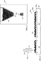
- a leadframe provides a stable support pad (1001 in FIG. 10 ) for firmly positioning the semiconductor chip (1010). Further, a leadframe offers a multitude of conductive leads (1003) to bring various electrical conductors into close proximity of the chip. Any remaining gap between the tip of the leads and the chip terminals is usually bridged by bonding wires (1030). Alternatively, in flip-chip technology the chip terminals may be connected to the leads by metal bumps.
- leadframe characteristics facilitate reliable adhesion to an attached chip and to packaging compounds (1070 in FIG. 10 ).
- adhesion may necessitate leadframe surface roughness, especially in view of the technical trend of shrinking package dimensions, which offers less surface area for adhesion.
- lead-free solders pushes the reflow temperature range into the neighborhood of about 260 °C, making it more difficult to maintain mold compound adhesion to the leadframes at elevated temperatures.
- a solvent paste which comprises a dispersant or solvent including nanoparticles of a second material.
- An example of a solvent paste is illustrated in FIG. 3 and designated 301.
- the nanoparticles, dissolved in the dispersant, are referred to as nanoparticles 302 of a second material.
- nanoparticles include spherical or other three-dimensional clusters composed of atoms or molecules, of inorganic or organic chemical compounds, of one-dimensional wires, of two-dimensional crystals and platelets, and of nanotubes.
- Nanoparticles 302 may be selected from a group including metals, metal oxides, oxides, and ceramics.
- the metals may include gold, silver, copper, aluminum, tin, zinc, and bismuth.
- Metal oxides may include copper oxide, which, as a mixture of cupric and cuprous oxide with a varying ratio, is known to offer better chemical adhesion to molding compounds than copper.
- a layer 200 of the solvent paste 301 which includes nanoparticles of the second material, is additively deposited on a surface 201a of the substrate 201 shown in FIG. 2 .
- Layer 200 may extend over the available two-dimensional surface area, or it may cover only portions of the surface area such as islands between about 0.1 ⁇ m to 100 ⁇ m dependent on the drop size of the solvent paste.
- the equipment for depositing the solvent paste includes a computer-controlled inkjet printer with a moving syringe 210 with nozzle 211, from which discrete drops 310 of the paste are released.
- Automated inkjet printers can be selected from a number of commercially available printers. Alternatively, a customized inkjet printer can be designed to work for specific pastes. Alternatively, any additive method can be used including inkjet printing, screen printing, gravure printing, dip coating, spray coating, and many others.
- the deposited layer 200 may extend along the lateral dimensions of the substrate 201, or may include, as depicted in FIG. 2 as example lengths 202 and 203, islands extending for about 0.1 ⁇ m to 100 ⁇ m length.
- layer 200 may cover the whole leadframe surface area of one or more leads, or selected parts such as the chip attach pad. Building up height from compiled drops of repeated runs of syringe 210, layer 200 may have a height 200a between about 100 nm and 500 nm, but may be thinner or considerably thicker.
- step 104 of the process flow of FIG. 1 energy is provided to elevate the temperature for sintering together the nanoparticles of the second material and concurrently for diffusing the second material into the substrate region adjoining the first surface, thereby anchoring the sintered nanoparticles of the second material to the first surface.
- the needed energy may be provided by a plurality of sources: thermal energy, photonic energy, electromagnetic energy, and chemical energy.
- the nanoparticles 302 are necking between the particles into a liquid network structure 402.
- the liquid network structure 402 is forming layer 400 in FIG. 4 .
- some second material is diffusing by atomic interdiffusion into the first material of the region adjoining the surface 201a (first surface) of substrate 201.
- the second material interdiffused into the region near surface 201a of substrate 201 is designated 402a.
- the diffusion depth is designated 402b in FIG. 4 .
- the atomic interdiffusion into the substrate creates an interdiffusion bond, which anchors layer 400 of sintered second nanoparticles into substrate 201.
- the liquid network structure 402 of second material is solidified to create a solid layer 400 of second material 402. Because the hardened network structure 400 remains at the substrate surface as a solid layer, the nanoparticles 402 of the second material are structural nanoparticles.
- another solvent paste which comprises a dispersant or solvent including nanoparticles of a third material.
- An example of a solvent paste is illustrated in FIG. 5 and designated 501.
- the nanoparticles, dissolved in the dispersant, are referred to as nanoparticles 502 of a third material.
- the third material may be selected from a group including polymers, oxides, ceramics, metals, and metal oxides.
- the metals may include gold, silver, copper, aluminum, tin, zinc, and bismuth, and the metal oxides may include copper oxide, which, as a mixture of cupric and cuprous oxide with a varying ratio, is known to offer better chemical adhesion to molding compounds than copper.
- the nanoparticles of the third material are selected so that they are operable to have adhesion to the nanoparticles of the second material. Due to intermolecular forces, the nanoparticles of the third material cling to the nanoparticles of the second material. In a related effect, an increase of surface tension, or surface energy, causes an increase of adhesion and wetting to a surface.
- FIG. 11 illustrates a nanoparticle 1100 with a core 1101 idealized as a smooth sphere of 5 nm diameter together with different hydrophobic ligand molecules drawn to scale and attached to the surface of core 1101.
- the ligand molecules in FIG. 11 illustrates a nanoparticle 1100 with a core 1101 idealized as a smooth sphere of 5 nm diameter together with different hydrophobic ligand molecules drawn to scale and attached to the surface of core 1101. The ligand molecules in FIG.
- molecule 1102 trioctylphosphine oxide, TOPO
- molecule 1104 triphenylphosphine, TPP
- molecule 1106 diodecanethiol, DDT
- molecule 1108 tetraoctylammonium bromide, TOAB
- molecule 1110 oleic acid, OA
- the cores of other nanoparticles may have hydrophilic ligand molecules attached to the core surface.
- hydrophilic ligand molecules include mercaptoacetic acid (MAA), mercaptopropionic acid (MPA), mercaptoundecanoic acid (MUA), mercaptosuccinic acid (MSA), dihydrolipic acid (DHLA), bis-sulphonated triphenylphosphine (mPEG 5 -SH, mPEG 45 -SH), and short peptide of sequence CALNN
- Ligand molecules such as inert molecular chains attached on the surface of the core can stabilize the nanoparticles against aggregation, while other ligand molecules attached on the surface can enhance the adhesion to objects.
- molecules of siloxane, silane, or the amine-group may be attached to the core surface to functionalize copper oxide nanoparticles.
- adhesion between the layer of the third material and the layer of the second material can be achieved, when the third material is the same chemical element as the second material but has different porosity or a different compound formulation leading to a different surface function.
- the third material may be a compound of the amine group or the silane group of the same element as the second material or the third material may belong to a different oxide formulation, such as CuO vs. Cu 2 O.
- the material density may be different, or the size or density of the porosity (regular vs. random configuration).
- the third material may have a different diffusion characteristic into solids along grain boundaries or lattice defects.
- a layer 500 of the solvent paste 501 which includes nanoparticles of the third material, is additively deposited on layer 200 of sintered nanoparticles of the second material.
- the process is illustrated in FIG. 5 ; the thickness of layer 500 of nanoparticles of the third material is 500a.
- Layer 500 may extend over the available two-dimensional surface area of substrate 201, or, as depicted in FIG. 5 as example lengths 503 and 504, it may cover only portions of the surface area such as islands between about 0.1 ⁇ m to 100 ⁇ m dependent on the drop size of the solvent paste.
- the equipment for the deposition includes a computer-controlled inkjet printer with a moving syringe 510 with nozzle 511, from which discrete drops 610 of the paste are discontinuously released.
- Automated inkjet printers can be selected from a number of commercially available printers. Alternatively, a customized inkjet printer can be designed to work for specific pastes. Alternatively, any additive method can be used including screen printing, gravure printing, flexographic printing, dip coating, spray coating, and inkjet printing comprising piezoelectric, thermal, acoustic and electrostatic inkjet printing.
- the deposited layer 500 may extend along the lateral dimensions of the whole substrate 201, or may, as depicted in FIG. 5 , include islands extending for about 0.1 ⁇ m to 100 ⁇ m length.
- layer 500 may cover the whole leadframe surface area of only one or more leads, or selected parts such as the chip attach pad. Building up height from compiled drops of repeated runs of syringe 510, layer 500 may preferably have a height 500a between about 100 nm and 500 nm, but may be thinner or considerably thicker.
- step 107 of the process flow shown in FIG. 1 energy is provided to increase the temperature for sintering together the nanoparticles of the third material.
- the needed energy may be provided by a plurality of sources: thermal energy, photonic energy, electromagnetic energy, and chemical energy.
- the nanoparticles 502 are necking between the particles into a liquid network structure. In the necking connections, the surfaces of the molten particles exhibit a constricted range resembling a neck between the particles.
- the liquid network structure is forming layer 500 in FIG. 4 .
- the liquid network structure of third material is solidified to create a solid layer 400 of third material.
- a bi-layer nanoparticle film 520 is formed.
- the thickness 520a of bi-layer film 520 is preferably between about 0.1 ⁇ m and 10 ⁇ m.
- the solid bi-layer nanoparticle film 520 together with at least portions of the substrate 201 of first material, are encapsulated into a package of polymeric compound.
- the process is illustrated in FIG. 7 , wherein the polymeric compound is denoted 701.
- a method for encapsulation by a polymeric compound is transfer molding technology using a thermoset epoxy-based molding compound. Because the compound has low viscosity at the elevated temperature during the molding process, the polymeric compound can readily fill any pores/voids 502a in the layer 500 of third material.
- the filling of the pores/voids by polymeric material takes place for any pores/voids, whether they are arrayed in an orderly pattern or in a random distribution, and whether they are shallow or in a random three-dimensional configuration including pores/voids resembling spherical caverns with narrow entrances.
- the polymeric compound 701 is hardened in the package and in the pores/voids.
- the polymeric-filled pores/voids represent an anchor of the package in the nanoparticle layer 500, giving strength to the interface of package (fourth material) and the bi-layer nanoparticle film (third material).
- layer 500 has adhesion to nanoparticle layer 400, giving the bi-layer film strength.
- layer 400 is anchored in metallic substrate 201 by metal interdiffusion 402a, giving the interface of the bi-layer film to the substrate strength.
- the bi-layer nanoparticle film improves the adhesion between the plastic package 701 and the metallic substrate 201. Adhesion improvements of an order of magnitude have been measured.
- the overall adhesion between two different materials can be improved by chemical adhesion. Consequently, the nanoparticles of the second material and third material can be chosen to enhance chemical adhesion.
- copper oxide nanoparticles have better chemical bonding to polymeric molding compounds than gold nanoparticles.
- FIG. 8 Another embodiment is a nanoparticle layer as depicted in FIG. 8 , which mixes the nanoparticles 402 of the second material and the nanoparticles 502 of the third material into a single homogeneous layer 800.
- Joint layer 800 improves the adhesion between substrate 201 and package 701 by averaging the adhesion at the two interfaces substrate 201 to layer 800, and package 701 to layer 800.
- the fabrication process for layer 800 is analogous to the fabrication processes described hereinabove for creating the nanoparticle layers 400 and 500.
- a computer-controlled inkjet printer is used with the solvent paste 901 comprising a mixture of nanoparticles 402 of the second material and nanoparticles 502 of the third material.
- the method for adhesion improvement between two objects by a sintered semi-homogeneous nanoparticle layer of two nanoparticle materials begins by providing an object of a first material and an object of a fourth material. Then, a solvent paste is provided, which includes a semi-homogeneous mixture of nanoparticles of a second material and nanoparticles of a third material.
- the nanoparticles of the second material are able to form diffusion bonds to the first material by molecular diffusion into the surface-near region of the substrate made of the first material.
- the nanoparticles of the third material form adhesion bonds by intermolecular forces to the nanoparticles of the second material, and further form to the object of the fourth material chemical bonds due to electrical forces and/or mechanical bonds due to filling of pores/voids.
- a layer of the semi-homogeneous mixture of the solvent paste is additively deposited on the surface of the object of the first material.
- Energy is then applied to elevate the temperature for sintering together the nanoparticles of the second and the third materials, forming a sintered nanoparticle layer, and for concurrently diffusing second material into the region adjoining the surface of the object of the first material.
- the object of the fourth material is brought into contact with the sintered nanoparticle layer so that the chemical and/or mechanical bonding is actualized; the object of the fourth material is bonded to the nanoparticles of the third material.
- FIG. 10 illustrates an example embodiment of the enhanced adhesion by a bi-layer nanoparticle adhesion film in an example semiconductor device, which includes a metallic leadframe and a plastic package.
- This example embodiment is a semiconductor device 1000 with a leadframe including a pad 1001 for assembling a semiconductor chip 1010, tie bars 1002 connecting pad 1001 to the sidewall of the package, and a plurality of leads 1003.
- the tie bars may be referred to as straps.
- the chip terminals are connected to the leads 1003 by bonding wires 1030, which commonly include ball bond 1031 and stitch bond 1032.
- bonding wires 1030 which commonly include ball bond 1031 and stitch bond 1032.
- leads 1003 are shaped as cantilevered leads; in other embodiments, the leads may have the shape of flat leads as used in Quad Flat No-Lead (QFN) devices or in Small Outline No-Lead (SON) devices.
- straps 1002 of the example device in FIG. 10 include bendings and steps, because pad 1001 and leads 1003 are not in the same plane. In other devices, straps 1002 are flat and planar, because pad 1001 and leads 1003 are in the same plane.
- portions of the leadframe are marked by dashing 1020, which include in a bi-layer film made of nanoparticles.
- the film may include voids of random distribution and random three-dimensional configurations.
- the example device 1000 includes a package 1070 for encapsulating chip 1010 and wire bonds 1030, any voids of the bi-layer film are filled by the polymeric compound.
- Package 1070 is made of a polymeric compound such as an epoxy-based thermoset polymer, formed in a molding process, and hardened by a polymerization process. The adhesion between the polymeric compound of package 1070 and the leadframe is improved by the bi-layer nanoparticle film. Other devices may have more and larger areas of the leadframe covered by the porous bi-layer nanoparticle film.
- example embodiments are applicable to active semiconductor devices with low and high pin counts, such as transistors and integrated circuits, and also to combinations of active and passive components on a leadframe pad.
- example embodiments are applicable to silicon-based semiconductor devices, and also to devices using gallium arsenide, gallium nitride, silicon germanium, and any other semiconductor material employed in industry. Further, example embodiments are applicable to leadframes with cantilevered leads and to QFN and SON type leadframes.
- example embodiments are applicable to laminated substrates and any other substrate or support structure to be bonded to a non-metallic body.
Landscapes
- Die Bonding (AREA)
- Structures Or Materials For Encapsulating Or Coating Semiconductor Devices Or Solid State Devices (AREA)
- Encapsulation Of And Coatings For Semiconductor Or Solid State Devices (AREA)
- Lead Frames For Integrated Circuits (AREA)
Applications Claiming Priority (2)
| Application Number | Priority Date | Filing Date | Title |
|---|---|---|---|
| US15/378,236 US20180166369A1 (en) | 2016-12-14 | 2016-12-14 | Bi-Layer Nanoparticle Adhesion Film |
| PCT/US2017/066495 WO2018112247A1 (en) | 2016-12-14 | 2017-12-14 | A bi-layer nanoparticle adhesion film |
Publications (3)
| Publication Number | Publication Date |
|---|---|
| EP3554823A1 EP3554823A1 (en) | 2019-10-23 |
| EP3554823A4 EP3554823A4 (en) | 2020-01-01 |
| EP3554823B1 true EP3554823B1 (en) | 2021-06-30 |
Family
ID=62489623
Family Applications (1)
| Application Number | Title | Priority Date | Filing Date |
|---|---|---|---|
| EP17880180.9A Active EP3554823B1 (en) | 2016-12-14 | 2017-12-14 | A bi-layer nanoparticle adhesion film |
Country Status (6)
| Country | Link |
|---|---|
| US (2) | US20180166369A1 (https=) |
| EP (1) | EP3554823B1 (https=) |
| JP (1) | JP7256343B2 (https=) |
| KR (1) | KR102516493B1 (https=) |
| CN (1) | CN109937137B (https=) |
| WO (1) | WO2018112247A1 (https=) |
Families Citing this family (9)
| Publication number | Priority date | Publication date | Assignee | Title |
|---|---|---|---|---|
| US20180138110A1 (en) * | 2016-11-17 | 2018-05-17 | Texas Instruments Incorporated | Enhanced Adhesion by Nanoparticle Layer Having Randomly Configured Voids |
| US9865527B1 (en) | 2016-12-22 | 2018-01-09 | Texas Instruments Incorporated | Packaged semiconductor device having nanoparticle adhesion layer patterned into zones of electrical conductance and insulation |
| US9941194B1 (en) | 2017-02-21 | 2018-04-10 | Texas Instruments Incorporated | Packaged semiconductor device having patterned conductance dual-material nanoparticle adhesion layer |
| JP7338204B2 (ja) * | 2019-04-01 | 2023-09-05 | 富士電機株式会社 | 半導体装置 |
| US10770206B1 (en) * | 2019-04-08 | 2020-09-08 | Government Of The United States As Represented By The Secretary Of The Air Force | System and method for fabricating a strain sensing device directly on a structure |
| US11116096B2 (en) | 2019-04-18 | 2021-09-07 | City University Of Hong Kong | Medium for binding components in an assembly of an electronic device, a method of preparing the same, a display assembly of an electronic device, and a system for simulating mechanical behaviours of the electronic device and the medium |
| JP7206418B2 (ja) * | 2019-11-28 | 2023-01-17 | 京セラ株式会社 | 配線基体、半導体素子収納用パッケージ、および半導体装置 |
| US12347805B2 (en) | 2023-05-11 | 2025-07-01 | Infineon Technologies Austria Ag | Inkjet printing of diffusion solder |
| US20250140653A1 (en) * | 2023-10-25 | 2025-05-01 | Texas Instruments Incorporated | Hybrid quad flat package electronic device |
Family Cites Families (36)
| Publication number | Priority date | Publication date | Assignee | Title |
|---|---|---|---|---|
| DE60221643T2 (de) * | 2001-02-16 | 2008-07-17 | OSAKA Titanium technologies Co., Ltd., Amagasaki | Gesinterter presskörper aus titanpulver |
| US20040161596A1 (en) * | 2001-05-31 | 2004-08-19 | Noriyuki Taoka | Porous ceramic sintered body and method of producing the same, and diesel particulate filter |
| DE10208635B4 (de) * | 2002-02-28 | 2010-09-16 | Infineon Technologies Ag | Diffusionslotstelle, Verbund aus zwei über eine Diffusionslotstelle verbundenen Teilen und Verfahren zur Herstellung der Diffusionslotstelle |
| WO2004054625A2 (en) * | 2002-12-12 | 2004-07-01 | Mykrolis Corporation | Porous sintered composite materials |
| US8257795B2 (en) * | 2004-02-18 | 2012-09-04 | Virginia Tech Intellectual Properties, Inc. | Nanoscale metal paste for interconnect and method of use |
| US20070163643A1 (en) * | 2004-02-19 | 2007-07-19 | Nanosolar, Inc. | High-throughput printing of chalcogen layer and the use of an inter-metallic material |
| JP4583063B2 (ja) * | 2004-04-14 | 2010-11-17 | 三井金属鉱業株式会社 | 銀化合物被覆銀粉及びその製造方法 |
| JP2006059904A (ja) * | 2004-08-18 | 2006-03-02 | Toshiba Corp | 半導体装置およびその製造方法 |
| DE102005028704B4 (de) * | 2005-06-20 | 2016-09-08 | Infineon Technologies Ag | Verfahren zur Herstellung eines Halbleiterbauteils mit in Kunststoffgehäusemasse eingebetteten Halbleiterbauteilkomponenten |
| DE102005061248B4 (de) * | 2005-12-20 | 2007-09-20 | Infineon Technologies Ag | Systemträger mit in Kunststoffmasse einzubettenden Oberflächen, Verfahren zur Herstellung eines Systemträgers und Verwendung einer Schicht als Haftvermittlerschicht |
| DE102006017115B4 (de) * | 2006-04-10 | 2008-08-28 | Infineon Technologies Ag | Halbleiterbauteil mit einem Kunststoffgehäuse und Verfahren zu seiner Herstellung |
| DE102006022254B4 (de) * | 2006-05-11 | 2008-12-11 | Infineon Technologies Ag | Halbleiterbauteil mit in Kunststoffgehäusemasse eingebetteten Halbleiterbauteilkomponenten, Anordnung für eine Mehrzahl von Halbleiterbauteilen und Verfahren zur Herstellung von Halbleiterbauteilen |
| WO2008068873A1 (en) * | 2006-12-08 | 2008-06-12 | Kazufumi Ogawa | Monolayer nanoparticle film, multilayer nanoparticle film, and manufacturing method thereof |
| JP2008153470A (ja) * | 2006-12-18 | 2008-07-03 | Renesas Technology Corp | 半導体装置および半導体装置の製造方法 |
| JP4895994B2 (ja) * | 2006-12-28 | 2012-03-14 | 株式会社日立製作所 | 金属粒子を用いた接合方法及び接合材料 |
| US20080272344A1 (en) * | 2007-03-23 | 2008-11-06 | Georgia Tech Research Corporation | Conductive polymer composites |
| JP5012239B2 (ja) * | 2007-06-13 | 2012-08-29 | 株式会社デンソー | 接合方法及び接合体 |
| US7846642B2 (en) * | 2007-08-17 | 2010-12-07 | The University Of Massachusetts | Direct incident beam lithography for patterning nanoparticles, and the articles formed thereby |
| US20090159121A1 (en) * | 2007-10-09 | 2009-06-25 | Nanomas Technologies, Inc. | Conductive nanoparticle inks and pastes and applications using the same |
| TWI456707B (zh) * | 2008-01-28 | 2014-10-11 | 瑞薩電子股份有限公司 | 半導體裝置及其製造方法 |
| JP4644718B2 (ja) | 2008-01-31 | 2011-03-02 | 株式会社日立製作所 | 金属/樹脂接着構造体及び樹脂封止型半導体装置とその製造方法 |
| US8513534B2 (en) * | 2008-03-31 | 2013-08-20 | Hitachi, Ltd. | Semiconductor device and bonding material |
| JP2010171271A (ja) | 2009-01-23 | 2010-08-05 | Renesas Technology Corp | 半導体装置およびその製造方法 |
| US20110209751A1 (en) * | 2010-01-25 | 2011-09-01 | Hitachi Chemical Company, Ltd. | Paste composition for electrode and photovoltaic cell |
| JP5525335B2 (ja) * | 2010-05-31 | 2014-06-18 | 株式会社日立製作所 | 焼結銀ペースト材料及び半導体チップ接合方法 |
| DE102010044709B4 (de) * | 2010-09-08 | 2015-07-02 | Vincotech Holdings S.à.r.l. | Leistungshalbleitermodul mit Metallsinterverbindungen sowie Herstellungsverfahren |
| US8736052B2 (en) * | 2011-08-22 | 2014-05-27 | Infineon Technologies Ag | Semiconductor device including diffusion soldered layer on sintered silver layer |
| DE102012207652A1 (de) * | 2012-05-08 | 2013-11-14 | Robert Bosch Gmbh | Zweistufiges Verfahren zum Fügen eines Halbleiters auf ein Substrat mit Verbindungsmaterial auf Silberbasis |
| US9583453B2 (en) * | 2012-05-30 | 2017-02-28 | Ormet Circuits, Inc. | Semiconductor packaging containing sintering die-attach material |
| JP2014127537A (ja) | 2012-12-26 | 2014-07-07 | Hitachi Power Semiconductor Device Ltd | 導電性接合材料を用いた半導体装置及びその半導体装置の製造方法。 |
| JP5975911B2 (ja) * | 2013-03-15 | 2016-08-23 | ルネサスエレクトロニクス株式会社 | 半導体装置 |
| US20150069600A1 (en) * | 2013-09-12 | 2015-03-12 | Texas Instruments Incorporated | Embedded Silver Nanomaterials into Die Backside to Enhance Package Performance and Reliability |
| KR102214829B1 (ko) * | 2014-02-27 | 2021-02-10 | 삼성전자주식회사 | 나노입자 다층 박막 |
| KR20190016142A (ko) * | 2014-06-12 | 2019-02-15 | 알파 어?블리 솔루션 인크. | 재료들의 소결 및 그를 이용하는 부착 방법들 |
| FR3038534A1 (fr) * | 2015-07-10 | 2017-01-13 | Commissariat Energie Atomique | Assemblage d'un element avec un substrat isole electriquement et a faible resistance thermique notamment pour des applications haute temperature, ensemble comprenant ledit assemblage et un drain thermique et procede de fabrication |
| FR3038535B1 (fr) * | 2015-07-10 | 2017-08-11 | Commissariat Energie Atomique | Assemblage comprenant deux elements de coefficient de dilatation thermique differents et un joint fritte heterogene en densite et procede de fabrication de l'assemblage |
-
2016
- 2016-12-14 US US15/378,236 patent/US20180166369A1/en not_active Abandoned
-
2017
- 2017-12-14 CN CN201780070261.2A patent/CN109937137B/zh active Active
- 2017-12-14 EP EP17880180.9A patent/EP3554823B1/en active Active
- 2017-12-14 WO PCT/US2017/066495 patent/WO2018112247A1/en not_active Ceased
- 2017-12-14 KR KR1020197016711A patent/KR102516493B1/ko active Active
- 2017-12-14 JP JP2019531942A patent/JP7256343B2/ja active Active
-
2025
- 2025-09-29 US US19/343,721 patent/US20260026366A1/en active Pending
Non-Patent Citations (1)
| Title |
|---|
| None * |
Also Published As
| Publication number | Publication date |
|---|---|
| EP3554823A1 (en) | 2019-10-23 |
| WO2018112247A1 (en) | 2018-06-21 |
| KR102516493B1 (ko) | 2023-04-03 |
| CN109937137B (zh) | 2021-07-13 |
| EP3554823A4 (en) | 2020-01-01 |
| JP2020513696A (ja) | 2020-05-14 |
| US20260026366A1 (en) | 2026-01-22 |
| JP7256343B2 (ja) | 2023-04-12 |
| CN109937137A (zh) | 2019-06-25 |
| US20180166369A1 (en) | 2018-06-14 |
| KR20190123718A (ko) | 2019-11-01 |
Similar Documents
| Publication | Publication Date | Title |
|---|---|---|
| US20260026366A1 (en) | Bi-Layer Nanoparticle Adhesion Film | |
| US10636679B2 (en) | Packaged semiconductor device having nanoparticle adhesion layer patterned into zones of electrical conductance and insulation | |
| JP7070971B2 (ja) | ランダムに構成されるボイドを有するナノ粒子層により高められた接着 | |
| US11296015B2 (en) | Die attach methods and semiconductor devices manufactured based on such methods | |
| US20080012101A1 (en) | Semiconductor Package Having Improved Adhesion and Solderability | |
| US20170051388A1 (en) | Mask-Less Selective Plating of Leadframe | |
| US12224251B2 (en) | Semiconductor device having cavities at an interface of an encapsulant and a die pad or leads | |
| US10573586B2 (en) | Packaged semiconductor device having patterned conductance dual-material nanoparticle adhesion layer | |
| CN112930588B (zh) | 半导体装置与烧结纳米粒子的连接 |
Legal Events
| Date | Code | Title | Description |
|---|---|---|---|
| STAA | Information on the status of an ep patent application or granted ep patent |
Free format text: STATUS: THE INTERNATIONAL PUBLICATION HAS BEEN MADE |
|
| PUAI | Public reference made under article 153(3) epc to a published international application that has entered the european phase |
Free format text: ORIGINAL CODE: 0009012 |
|
| STAA | Information on the status of an ep patent application or granted ep patent |
Free format text: STATUS: REQUEST FOR EXAMINATION WAS MADE |
|
| 17P | Request for examination filed |
Effective date: 20190715 |
|
| AK | Designated contracting states |
Kind code of ref document: A1 Designated state(s): AL AT BE BG CH CY CZ DE DK EE ES FI FR GB GR HR HU IE IS IT LI LT LU LV MC MK MT NL NO PL PT RO RS SE SI SK SM TR |
|
| AX | Request for extension of the european patent |
Extension state: BA ME |
|
| A4 | Supplementary search report drawn up and despatched |
Effective date: 20191129 |
|
| RIC1 | Information provided on ipc code assigned before grant |
Ipc: H01L 23/31 20060101ALI20191125BHEP Ipc: B82B 1/00 20060101ALI20191125BHEP Ipc: B82Y 30/00 20110101ALI20191125BHEP Ipc: B32B 5/22 20060101AFI20191125BHEP Ipc: H01L 23/495 20060101ALI20191125BHEP |
|
| DAV | Request for validation of the european patent (deleted) | ||
| DAX | Request for extension of the european patent (deleted) | ||
| GRAP | Despatch of communication of intention to grant a patent |
Free format text: ORIGINAL CODE: EPIDOSNIGR1 |
|
| STAA | Information on the status of an ep patent application or granted ep patent |
Free format text: STATUS: GRANT OF PATENT IS INTENDED |
|
| INTG | Intention to grant announced |
Effective date: 20210113 |
|
| GRAS | Grant fee paid |
Free format text: ORIGINAL CODE: EPIDOSNIGR3 |
|
| GRAA | (expected) grant |
Free format text: ORIGINAL CODE: 0009210 |
|
| STAA | Information on the status of an ep patent application or granted ep patent |
Free format text: STATUS: THE PATENT HAS BEEN GRANTED |
|
| AK | Designated contracting states |
Kind code of ref document: B1 Designated state(s): AL AT BE BG CH CY CZ DE DK EE ES FI FR GB GR HR HU IE IS IT LI LT LU LV MC MK MT NL NO PL PT RO RS SE SI SK SM TR |
|
| REG | Reference to a national code |
Ref country code: CH Ref legal event code: EP |
|
| REG | Reference to a national code |
Ref country code: AT Ref legal event code: REF Ref document number: 1405981 Country of ref document: AT Kind code of ref document: T Effective date: 20210715 |
|
| REG | Reference to a national code |
Ref country code: DE Ref legal event code: R096 Ref document number: 602017041449 Country of ref document: DE |
|
| REG | Reference to a national code |
Ref country code: IE Ref legal event code: FG4D |
|
| REG | Reference to a national code |
Ref country code: LT Ref legal event code: MG9D |
|
| PG25 | Lapsed in a contracting state [announced via postgrant information from national office to epo] |
Ref country code: BG Free format text: LAPSE BECAUSE OF FAILURE TO SUBMIT A TRANSLATION OF THE DESCRIPTION OR TO PAY THE FEE WITHIN THE PRESCRIBED TIME-LIMIT Effective date: 20210930 Ref country code: HR Free format text: LAPSE BECAUSE OF FAILURE TO SUBMIT A TRANSLATION OF THE DESCRIPTION OR TO PAY THE FEE WITHIN THE PRESCRIBED TIME-LIMIT Effective date: 20210630 Ref country code: FI Free format text: LAPSE BECAUSE OF FAILURE TO SUBMIT A TRANSLATION OF THE DESCRIPTION OR TO PAY THE FEE WITHIN THE PRESCRIBED TIME-LIMIT Effective date: 20210630 |
|
| REG | Reference to a national code |
Ref country code: NL Ref legal event code: MP Effective date: 20210630 |
|
| REG | Reference to a national code |
Ref country code: AT Ref legal event code: MK05 Ref document number: 1405981 Country of ref document: AT Kind code of ref document: T Effective date: 20210630 |
|
| PG25 | Lapsed in a contracting state [announced via postgrant information from national office to epo] |
Ref country code: GR Free format text: LAPSE BECAUSE OF FAILURE TO SUBMIT A TRANSLATION OF THE DESCRIPTION OR TO PAY THE FEE WITHIN THE PRESCRIBED TIME-LIMIT Effective date: 20211001 Ref country code: RS Free format text: LAPSE BECAUSE OF FAILURE TO SUBMIT A TRANSLATION OF THE DESCRIPTION OR TO PAY THE FEE WITHIN THE PRESCRIBED TIME-LIMIT Effective date: 20210630 Ref country code: SE Free format text: LAPSE BECAUSE OF FAILURE TO SUBMIT A TRANSLATION OF THE DESCRIPTION OR TO PAY THE FEE WITHIN THE PRESCRIBED TIME-LIMIT Effective date: 20210630 Ref country code: NO Free format text: LAPSE BECAUSE OF FAILURE TO SUBMIT A TRANSLATION OF THE DESCRIPTION OR TO PAY THE FEE WITHIN THE PRESCRIBED TIME-LIMIT Effective date: 20210930 Ref country code: LV Free format text: LAPSE BECAUSE OF FAILURE TO SUBMIT A TRANSLATION OF THE DESCRIPTION OR TO PAY THE FEE WITHIN THE PRESCRIBED TIME-LIMIT Effective date: 20210630 |
|
| PG25 | Lapsed in a contracting state [announced via postgrant information from national office to epo] |
Ref country code: ES Free format text: LAPSE BECAUSE OF FAILURE TO SUBMIT A TRANSLATION OF THE DESCRIPTION OR TO PAY THE FEE WITHIN THE PRESCRIBED TIME-LIMIT Effective date: 20210630 Ref country code: EE Free format text: LAPSE BECAUSE OF FAILURE TO SUBMIT A TRANSLATION OF THE DESCRIPTION OR TO PAY THE FEE WITHIN THE PRESCRIBED TIME-LIMIT Effective date: 20210630 Ref country code: SM Free format text: LAPSE BECAUSE OF FAILURE TO SUBMIT A TRANSLATION OF THE DESCRIPTION OR TO PAY THE FEE WITHIN THE PRESCRIBED TIME-LIMIT Effective date: 20210630 Ref country code: SK Free format text: LAPSE BECAUSE OF FAILURE TO SUBMIT A TRANSLATION OF THE DESCRIPTION OR TO PAY THE FEE WITHIN THE PRESCRIBED TIME-LIMIT Effective date: 20210630 Ref country code: AT Free format text: LAPSE BECAUSE OF FAILURE TO SUBMIT A TRANSLATION OF THE DESCRIPTION OR TO PAY THE FEE WITHIN THE PRESCRIBED TIME-LIMIT Effective date: 20210630 Ref country code: CZ Free format text: LAPSE BECAUSE OF FAILURE TO SUBMIT A TRANSLATION OF THE DESCRIPTION OR TO PAY THE FEE WITHIN THE PRESCRIBED TIME-LIMIT Effective date: 20210630 Ref country code: PT Free format text: LAPSE BECAUSE OF FAILURE TO SUBMIT A TRANSLATION OF THE DESCRIPTION OR TO PAY THE FEE WITHIN THE PRESCRIBED TIME-LIMIT Effective date: 20211102 Ref country code: NL Free format text: LAPSE BECAUSE OF FAILURE TO SUBMIT A TRANSLATION OF THE DESCRIPTION OR TO PAY THE FEE WITHIN THE PRESCRIBED TIME-LIMIT Effective date: 20210630 Ref country code: RO Free format text: LAPSE BECAUSE OF FAILURE TO SUBMIT A TRANSLATION OF THE DESCRIPTION OR TO PAY THE FEE WITHIN THE PRESCRIBED TIME-LIMIT Effective date: 20210630 |
|
| PG25 | Lapsed in a contracting state [announced via postgrant information from national office to epo] |
Ref country code: PL Free format text: LAPSE BECAUSE OF FAILURE TO SUBMIT A TRANSLATION OF THE DESCRIPTION OR TO PAY THE FEE WITHIN THE PRESCRIBED TIME-LIMIT Effective date: 20210630 |
|
| REG | Reference to a national code |
Ref country code: DE Ref legal event code: R097 Ref document number: 602017041449 Country of ref document: DE |
|
| PG25 | Lapsed in a contracting state [announced via postgrant information from national office to epo] |
Ref country code: DK Free format text: LAPSE BECAUSE OF FAILURE TO SUBMIT A TRANSLATION OF THE DESCRIPTION OR TO PAY THE FEE WITHIN THE PRESCRIBED TIME-LIMIT Effective date: 20210630 |
|
| PLBE | No opposition filed within time limit |
Free format text: ORIGINAL CODE: 0009261 |
|
| STAA | Information on the status of an ep patent application or granted ep patent |
Free format text: STATUS: NO OPPOSITION FILED WITHIN TIME LIMIT |
|
| PG25 | Lapsed in a contracting state [announced via postgrant information from national office to epo] |
Ref country code: AL Free format text: LAPSE BECAUSE OF FAILURE TO SUBMIT A TRANSLATION OF THE DESCRIPTION OR TO PAY THE FEE WITHIN THE PRESCRIBED TIME-LIMIT Effective date: 20210630 |
|
| 26N | No opposition filed |
Effective date: 20220331 |
|
| PG25 | Lapsed in a contracting state [announced via postgrant information from national office to epo] |
Ref country code: MC Free format text: LAPSE BECAUSE OF FAILURE TO SUBMIT A TRANSLATION OF THE DESCRIPTION OR TO PAY THE FEE WITHIN THE PRESCRIBED TIME-LIMIT Effective date: 20210630 Ref country code: IT Free format text: LAPSE BECAUSE OF FAILURE TO SUBMIT A TRANSLATION OF THE DESCRIPTION OR TO PAY THE FEE WITHIN THE PRESCRIBED TIME-LIMIT Effective date: 20210630 |
|
| REG | Reference to a national code |
Ref country code: CH Ref legal event code: PL |
|
| REG | Reference to a national code |
Ref country code: BE Ref legal event code: MM Effective date: 20211231 |
|
| PG25 | Lapsed in a contracting state [announced via postgrant information from national office to epo] |
Ref country code: LU Free format text: LAPSE BECAUSE OF NON-PAYMENT OF DUE FEES Effective date: 20211214 Ref country code: IE Free format text: LAPSE BECAUSE OF NON-PAYMENT OF DUE FEES Effective date: 20211214 |
|
| PG25 | Lapsed in a contracting state [announced via postgrant information from national office to epo] |
Ref country code: BE Free format text: LAPSE BECAUSE OF NON-PAYMENT OF DUE FEES Effective date: 20211231 |
|
| PG25 | Lapsed in a contracting state [announced via postgrant information from national office to epo] |
Ref country code: LI Free format text: LAPSE BECAUSE OF NON-PAYMENT OF DUE FEES Effective date: 20211231 Ref country code: CH Free format text: LAPSE BECAUSE OF NON-PAYMENT OF DUE FEES Effective date: 20211231 |
|
| PG25 | Lapsed in a contracting state [announced via postgrant information from national office to epo] |
Ref country code: LT Free format text: LAPSE BECAUSE OF FAILURE TO SUBMIT A TRANSLATION OF THE DESCRIPTION OR TO PAY THE FEE WITHIN THE PRESCRIBED TIME-LIMIT Effective date: 20210630 |
|
| P01 | Opt-out of the competence of the unified patent court (upc) registered |
Effective date: 20230523 |
|
| PG25 | Lapsed in a contracting state [announced via postgrant information from national office to epo] |
Ref country code: CY Free format text: LAPSE BECAUSE OF FAILURE TO SUBMIT A TRANSLATION OF THE DESCRIPTION OR TO PAY THE FEE WITHIN THE PRESCRIBED TIME-LIMIT Effective date: 20210630 |
|
| PG25 | Lapsed in a contracting state [announced via postgrant information from national office to epo] |
Ref country code: HU Free format text: LAPSE BECAUSE OF FAILURE TO SUBMIT A TRANSLATION OF THE DESCRIPTION OR TO PAY THE FEE WITHIN THE PRESCRIBED TIME-LIMIT; INVALID AB INITIO Effective date: 20171214 |
|
| PG25 | Lapsed in a contracting state [announced via postgrant information from national office to epo] |
Ref country code: MK Free format text: LAPSE BECAUSE OF FAILURE TO SUBMIT A TRANSLATION OF THE DESCRIPTION OR TO PAY THE FEE WITHIN THE PRESCRIBED TIME-LIMIT Effective date: 20210630 |
|
| PG25 | Lapsed in a contracting state [announced via postgrant information from national office to epo] |
Ref country code: MT Free format text: LAPSE BECAUSE OF FAILURE TO SUBMIT A TRANSLATION OF THE DESCRIPTION OR TO PAY THE FEE WITHIN THE PRESCRIBED TIME-LIMIT Effective date: 20210630 |
|
| PG25 | Lapsed in a contracting state [announced via postgrant information from national office to epo] |
Ref country code: TR Free format text: LAPSE BECAUSE OF FAILURE TO SUBMIT A TRANSLATION OF THE DESCRIPTION OR TO PAY THE FEE WITHIN THE PRESCRIBED TIME-LIMIT Effective date: 20210630 |
|
| PGFP | Annual fee paid to national office [announced via postgrant information from national office to epo] |
Ref country code: DE Payment date: 20251126 Year of fee payment: 9 |
|
| PGFP | Annual fee paid to national office [announced via postgrant information from national office to epo] |
Ref country code: GB Payment date: 20251119 Year of fee payment: 9 |
|
| PGFP | Annual fee paid to national office [announced via postgrant information from national office to epo] |
Ref country code: FR Payment date: 20251120 Year of fee payment: 9 |