EP3553693A1 - Fingerabdruckerkennungsmodul, fingerabdruckerkennungsverfahren und entsprechendes produkt - Google Patents
Fingerabdruckerkennungsmodul, fingerabdruckerkennungsverfahren und entsprechendes produkt Download PDFInfo
- Publication number
- EP3553693A1 EP3553693A1 EP17893077.2A EP17893077A EP3553693A1 EP 3553693 A1 EP3553693 A1 EP 3553693A1 EP 17893077 A EP17893077 A EP 17893077A EP 3553693 A1 EP3553693 A1 EP 3553693A1
- Authority
- EP
- European Patent Office
- Prior art keywords
- fingerprint
- electronic device
- frequency
- collection signal
- charging
- Prior art date
- Legal status (The legal status is an assumption and is not a legal conclusion. Google has not performed a legal analysis and makes no representation as to the accuracy of the status listed.)
- Withdrawn
Links
Images



Classifications
-
- G—PHYSICS
- G06—COMPUTING OR CALCULATING; COUNTING
- G06V—IMAGE OR VIDEO RECOGNITION OR UNDERSTANDING
- G06V40/00—Recognition of biometric, human-related or animal-related patterns in image or video data
- G06V40/10—Human or animal bodies, e.g. vehicle occupants or pedestrians; Body parts, e.g. hands
- G06V40/12—Fingerprints or palmprints
- G06V40/1365—Matching; Classification
-
- G—PHYSICS
- G06—COMPUTING OR CALCULATING; COUNTING
- G06V—IMAGE OR VIDEO RECOGNITION OR UNDERSTANDING
- G06V40/00—Recognition of biometric, human-related or animal-related patterns in image or video data
- G06V40/10—Human or animal bodies, e.g. vehicle occupants or pedestrians; Body parts, e.g. hands
- G06V40/12—Fingerprints or palmprints
- G06V40/13—Sensors therefor
-
- G—PHYSICS
- G06—COMPUTING OR CALCULATING; COUNTING
- G06V—IMAGE OR VIDEO RECOGNITION OR UNDERSTANDING
- G06V40/00—Recognition of biometric, human-related or animal-related patterns in image or video data
- G06V40/10—Human or animal bodies, e.g. vehicle occupants or pedestrians; Body parts, e.g. hands
- G06V40/12—Fingerprints or palmprints
- G06V40/13—Sensors therefor
- G06V40/1306—Sensors therefor non-optical, e.g. ultrasonic or capacitive sensing
-
- G—PHYSICS
- G06—COMPUTING OR CALCULATING; COUNTING
- G06V—IMAGE OR VIDEO RECOGNITION OR UNDERSTANDING
- G06V40/00—Recognition of biometric, human-related or animal-related patterns in image or video data
- G06V40/10—Human or animal bodies, e.g. vehicle occupants or pedestrians; Body parts, e.g. hands
- G06V40/12—Fingerprints or palmprints
- G06V40/13—Sensors therefor
- G06V40/1329—Protecting the fingerprint sensor against damage caused by the finger
Definitions
- the present application relates to the field of communications, and in particular, to a fingerprint identification assembly, a fingerprint identification method, and related products.
- a sensor of a fingerprint identification assembly emits a fingerprint collection signal (for example, a square-wave signal, a sinusoidal signal, etc.), and data of a fingerprint image can be obtained as a capacitance between a finger and the sensor is formed from the fingerprint collection signal.
- a fingerprint collection signal for example, a square-wave signal, a sinusoidal signal, etc.
- a fingerprint identification assembly, a fingerprint identification method, and related products are provided in embodiments of the present disclosure, which can reduce noise interference from a charger on a fingerprint image when the electronic device is charged.
- a fingerprint identification assembly applied in an electronic device includes a fingerprint chip, a cover, and a base.
- a cover is disposed at one side of the fingerprint chip;
- a base is disposed at other side of the fingerprint chip away from the cover, configured to support the fingerprint chip and the cover; wherein the charging fingerprint collection signal is configured to collect data of a user's fingerprint image, a frequency of the charging fingerprint collection signal is greater than a preset frequency, and the preset frequency is a switching frequency of the charger of the electronic device.
- a fingerprint identification method applied in an electronic device is provided.
- the method is applied to an electronic device and includes:
- a fingerprint identification apparatus applied in an electronic device which includes:
- an electronic device which includes a processor, a memory, and a communication interface, the processor being coupled to the memory and the communication interface;
- the memory stores executable program codes, the communication interface is configured for wireless communication;
- the processor is configured to invoke the executable program code in the memory to perform a method in the second aspect of the present disclosure.
- a computer storage medium stores a computer program, wherein the computer program causes a computer to perform a part of or all of blocks in the second aspect of the present disclosure.
- a computer program product in an embodiment of the present disclosure.
- the computer program product includes a non-transitory computer readable storage medium storing a computer program, wherein the computer program being configured to cause a computer to perform a part of or all of blocks in the second aspect of the present disclosure.
- the computer program product may be a software installation package.
- the electronic device receives the fingerprint collection instruction; emits the charging fingerprint collection signal is emitted, the frequency of the charging fingerprint collection signal is greater than the preset frequency, the preset frequency is the switching frequency of the charger of the electronic device, and the charging fingerprint collection signal is used for collecting data of the user's fingerprint image.
- the electronic device can emit a charging fingerprint collection signal of which a frequency is greater than a switching frequency of the charger to collect data of a user's fingerprint image.
- the charging fingerprint collection signal is offset from the switching frequency of the charger, which avoids interference from voltage output by the charger on the charging fingerprint collection signal and then can reduce the noise interference from the charger on data of the fingerprint image when the electronic device is charged.
- first”, “second” and “third” in the present application are used to distinguish different objects, and are not intended to describe a specific order.
- the terms “comprise” and “have” and variations thereof are intended to cover a non-exclusive inclusion.
- a process, a method, a system, a product, or a device that comprises a series of steps or units is not limited to the listed steps or units, but optionally includes steps or units not listed, or optionally include other steps or units inherent to these processes, methods, products or devices.
- the electronic device involved in the embodiments of the present disclosure may include various handheld devices (such as mobile phones) having wireless communication functions, in-vehicle devices, wearable devices, computing devices or other processing devices connected to the wireless modem, and various forms of user equipment (UE), a mobile station (MS), a terminal device, and the like.
- UE user equipment
- MS mobile station
- terminal device a terminal device
- the devices mentioned above are collectively referred to as electronic devices.
- the mobile phone when the mobile phone is charged, a switching frequency of a charger of the mobile phone closes to an emission frequency of the fingerprint collection signal, and the noise generated by the charger of the mobile phone may bring interference on data of a fingerprint image collected by the fingerprint identification assembly, resulting in the collected data of the fingerprint image is distorted. Therefore, a fingerprint identification method is provided in an embodiment of the present disclosure, which is applied to an electronic device and includes:
- FIG. 1a is a schematic structural diagram of a fingerprint identification assembly according to an embodiment of the present disclosure.
- the fingerprint identification assembly 10 includes a fingerprint chip 101, a cover 102 and a base 103.
- the cover 102 is disposed at one side of the fingerprint chip 101.
- the base 103 is disposed at the other side of the fingerprint chip 101 away from the cover 102.
- the base 103 is configured to support the fingerprint chip 101 and the cover 102.
- the fingerprint chip 101 is configured to emit a charging fingerprint collection signal, and a frequency of the charging fingerprint collection signal is greater than a preset frequency.
- the preset frequency is a switching frequency of a charger of an electronic device, and the charging fingerprint collection signal is used to collect data of a user's fingerprint image.
- the electronic device can emit the charging fingerprint collection signal by using the fingerprint identification assembly in the electronic device, and the frequency of the charging fingerprint collection signal is greater than the switching frequency of the charger.
- the electronic device ensures that the electronic device can has no interference from signals output by the charger when the electronic device is in the charging state.
- FIG. 1b is a schematic structural diagram of another fingerprint identification assembly according to in an embodiment of the present disclosure.
- the fingerprint identification assembly 10 shown in FIG. 1b further includes a metal ring 104.
- the metal ring 104 is disposed around the cover 102.
- the metal ring 104 is also called as a fingerprint decoration ring, a fingerprint bezel, or a fingerprint ring.
- a manner in which the metal ring 104 is disposed around the cover 102 may be that the metal ring 104 is electrically connected to and surrounds the cover 102.
- the metal ring 104 may has a shape of one or a combination of a circle, an ellipse, a rectangle, and a polygon.
- the material of the metal ring 104 may be stainless steel, gold, silver, copper or the like.
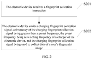
- FIG. 2 is a schematic flowchart of a fingerprint identification method according to an embodiment of the present disclosure. As shown in FIG. 2 , the method includes actions/operations in the following blocks.
- the electronic device receives a fingerprint collection instruction.
- the fingerprint collection instruction received by the electronic device may be input by a user's voice, or may be generated after the electronic device senses that the fingerprint of the user contacts the fingerprint identification assembly.
- the fingerprint collection instruction is used to trigger the electronic device to enable the fingerprint collection function and then trigger the electronic device to emit the fingerprint collection signal.
- the electronic device emits a charging fingerprint collection signal, wherein a frequency of the charging fingerprint collection signal is greater than a preset frequency, the preset frequency is a switching frequency of a charger of the electronic device, and the charging fingerprint collection signal is used to collect data of a user's fingerprint image.
- the electronic device can emit the charging fingerprint collection signal by using the fingerprint identification assembly in the electronic device, and the frequency of the charging fingerprint collection signal is greater than the switching frequency of the charger, thus, it ensures that the electronic device can have no interference from the signals output by the charger when the electronic device is in the charging state.
- the switching frequency of the charger refers to a frequency of a voltage signal (for example, the voltage pulse signal) output by the charger.
- the frequency of the voltage pulse signal output by the charger is generally hundreds of KHz. For example, when the frequency of the voltage pulse signal output by the charger is 500 kHz, the frequency at which the fingerprint identification assembly emits the charging fingerprint collection signal can be set to be 1.5 MHz.
- the charging fingerprint collection signal is used to collect data of a user's fingerprint image.
- an amplitude of the charging fingerprint collection signal is greater than a preset amplitude, and the preset amplitude is a magnitude of a voltage signal output by the charger.
- the amplitude of the charging fingerprint collection signal may be set to be greater than the amplitude of the voltage signal output by the charger.
- the amplitude of the charging fingerprint collection signal can be set to be 6V.
- the electronic device can emit a charging fingerprint collection signal of which a frequency is greater than a switching frequency of the charger to collect data of a user's fingerprint image.
- the charging fingerprint collection signal is offset from the switching frequency of the charger, which avoids interference from voltage output by the charger on the charging fingerprint collection signal and then can reduce the noise interference from the charger on data of the fingerprint image when the electronic device is charged.
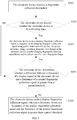
- FIG. 3 is a schematic flowchart of another fingerprint identification method disclosed in an embodiment of the present disclosure. As shown in FIG. 3 , the fingerprint identification method includes actions/operations in the following blocks.
- the electronic device receives a fingerprint collection instruction.
- the block S301 can be referred to the block S201 shown in FIG. 2 , which will not be repeated herein.
- the electronic device detects whether the electronic device is in a charging state. If yes, block S303 is performed, and if no, block S304 is performed.
- the electronic device can detect whether the electronic device is in the charging state by using a charging IC in the electronic device.
- the electronic device detects that the electronic device is in the charging state, the electronic device emits a charging fingerprint collection signal.
- block S304 is performed.
- the electronic device emits a charging fingerprint collection signal, wherein a frequency of the charging fingerprint collection signal is greater than a preset frequency, the preset frequency is a switching frequency of a charger of the electronic device, and the charging fingerprint collection signal is used to collect data of a user's fingerprint image.
- the frequency of the charging fingerprint collection signal is greater than the switching frequency of the charger of the electronic device. Further, the difference between the frequency of the charging fingerprint collection signal and the switching frequency of the charger of the electronic device meets certain conditions. Assume that the frequency of the charging fingerprint collection signal is f1 and the switching frequency of the charger is f2, f1 and f2 then meet at least one of the following conditions:
- the electronic device determines whether a difference between a frequency of a display signal of the electronic device and a frequency of a normal fingerprint collection signal is greater than a preset threshold. If yes, the block S303 is performed, and if no, block S305 is performed.
- the electronic device determines whether the difference between the frequency of the display signal of the electronic device and the frequency of the normal fingerprint collection signal is greater than a preset threshold.
- the display signal of the electronic device may has a frequency which any signal displayed on a display in the electronic device has, for example, a refresh frequency of the display in the electronic device.
- the frequency of the display signal of the electronic device may also refer to a display frequency of each row of the liquid crystal display transistors of the liquid crystal display in the electronic device.
- the preset threshold may be set to be one of f1 ⁇ 50%, f2 ⁇ 50%, f1 ⁇ 80%, f2 ⁇ 80%, f1 ⁇ 90%, and f2 ⁇ 90%.
- the electronic device emits a display fingerprint collection signal, wherein a difference between a frequency of the display fingerprint collection signal and the frequency of the normal fingerprint collection signal is greater than a preset threshold.
- the electronic device when the difference between the frequency of the display signal of the electronic device and the frequency of the normal fingerprint collection signal is less than or equal to a preset threshold, the electronic device emits the display fingerprint collection signal.
- the difference between the frequency of the display fingerprint collection signal and the frequency of the normal fingerprint collection signal is greater than a preset threshold.
- the difference between an amplitude of the display fingerprint collection signal and an amplitude of the display signal of the electronic device is greater than a preset amplitude.
- the difference between the amplitude of the display fingerprint collection signal and the amplitude of the display signal of the electronic device may be set to be greater than a preset amplitude.
- the preset amplitude can be preset and stored in a non-volatile memory of the electronic device.
- the amplitude of the display fingerprint collection signal may be set to 6V.
- the electronic device when the electronic device is in the charging state, the electronic device may emit the charging fingerprint collection signal of which the frequency is greater than a switching frequency of the charger to collect data of user's fingerprint image, so that the frequency of the charging fingerprint collection signal is offset from the charging frequency of the charger, which avoids interference from the voltage signals output by the charger on the charging fingerprint collection signal, and then can reduce the noise interference from the charger on the fingerprint image when the electronic device is charged.
- the electronic device may emit the display fingerprint collection signal of which frequency is greater than that of the normal fingerprint collection signal with a preset threshold, so that the frequency of the display fingerprint collection signal is offset from the frequency of the display signal of the electronic device, which avoids interference from the display signal of the electronic device on the charging fingerprint collection signal.
- the electronic device includes corresponding hardware structures and/or software modules for performing the respective functions in order to implement the above functions.
- the present disclosure can be implemented by hardware or a combination of hardware and computer software, combined with the elements and algorithm steps of the various examples described in embodiments disclosed herein. Whether a function is implemented by hardware or a way that the computer software drives hardware depends on specific applications and design constraints of the solution. A person skilled in the art can use different methods for each particular application to implement the described functionality, but such implementation should not be considered to be beyond the scope of the disclosure.
- the electronic device may be divided into functional units according to the foregoing method example.
- each functional unit may be obtained according to each function.
- Two or more functions may also be integrated into one processing unit.
- the above integrated unit can be implemented in the form of hardware or in the form of a software functional unit. It should be noted that the unit-division in the embodiment of the present disclosure is schematic, and is only a logical function division. In an actual implementation, there may be another division manner.
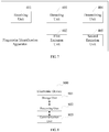
- FIG. 4 is a schematic structural diagram of a fingerprint identification apparatus according to an embodiment of the present disclosure.
- the fingerprint identification apparatus is applied to an electronic device.
- the fingerprint identification apparatus includes a receiving unit 401 and a first emission unit 402.
- the receiving unit 401 is configured to receive a fingerprint collection instruction.
- the first emission unit 402 is configured to emit a charging fingerprint collection signal, wherein a frequency of the charging fingerprint collection signal is greater than a preset frequency, the preset frequency is a switching frequency of a charger of the electronic device, and the charging fingerprint collection signal is used to collect data of a user's fingerprint image.
- the electronic device can emit a charging fingerprint collection signal of which a frequency is greater than a switching frequency of the charger to collect data of a user's fingerprint image.
- the charging fingerprint collection signal is offset from the switching frequency of the charger, which avoids interference from voltage output by the charger on the charging fingerprint collection signal and then can reduce the noise interference from the charger on data of the fingerprint image when the electronic device is charged.
- the receiving unit 401 receives the fingerprint collection instruction in the following manner: user voice input or sensing user's fingerprint contacts on the fingerprint identification assembly.
- the implementation of the fingerprint identification apparatus shown in FIG. 4 may be referred to the method embodiment shown in FIG. 2 , which is not described herein again.
- FIG. 5 is a schematic structural diagram of another fingerprint identification apparatus disclosed in the embodiment of the present disclosure. What described in FIG. 5 is obtained by further optimizing based on FIG. 4 .
- the fingerprint identification apparatus further includes a detecting unit 403 in addition to the receiving unit 401 and the first emission unit 402 as shown in FIG. 4 .
- the detecting unit 403 is configured to detect whether the electronic device is in a charging state.
- the first emission unit 402 is further configured to emit the charging fingerprint collection signal when the detecting unit 403 detects that the electronic device is in the charging state.
- the implementation of the fingerprint identification apparatus shown in FIG. 5 may be referred to the method embodiment shown in FIG. 3 , which is not described herein again.
- FIG. 6 is a schematic structural diagram of another fingerprint identification apparatus disclosed in the embodiment of the present disclosure. What described in FIG. 6 is obtained by further optimizing based on FIG. 5 .
- the fingerprint identification apparatus further includes a determining unit 404 in addition to the receiving unit 401, the first emission unit 402, and the detecting unit 403 as shown in FIG. 5 .
- the determining unit 404 is configured to determine whether the difference between the frequency of the display signal of the electronic device and the frequency of the normal fingerprint collection signal is greater than a preset threshold when the detecting unit 403 detects that the electronic device is not in the charging state.
- the first emission unit 402 is further configured to emit the charging fingerprint collection signal when the determining unit 404 determines that the result is YES.
- the implementation of the fingerprint identification apparatus shown in FIG. 6 may be referred to the method embodiment as shown in FIG. 3 , which is not described herein again.
- FIG. 7 is a schematic structural diagram of another fingerprint identification apparatus disclosed in the embodiment of the present disclosure. What described in FIG. 7 is obtained by further optimizing based on FIG. 6 .
- the fingerprint identification apparatus further includes a second emission unit 405 in addition to the receiving unit 401, the first emission unit 402, the detecting unit 403, and the determining unit 404 as shown in FIG. 6 .
- the second emission unit 405 is further configured to emit a display fingerprint collection signal when the determining unit 404 determines that the result is no, wherein the difference between the frequency of the display fingerprint collection signal and the frequency of the normal fingerprint collection signal is greater than a preset threshold.
- the electronic device may emit the charging fingerprint collection signal of which the frequency is greater than a switching frequency of the charger to collect data of user's fingerprint image, so that the frequency of the charging fingerprint collection signal is offset from the charging frequency of the charger, which avoids interference from the voltage signals output by the charger on the charging fingerprint collection signal, and then can reduce the noise interference from the charger on the fingerprint image when the electronic device is charged.
- the electronic device may emit the display fingerprint collection signal of which frequency is greater than that of the normal fingerprint collection signal with a preset threshold, so that the frequency of the display fingerprint collection signal is offset from the frequency of the display signal of the electronic device, which avoids interference from the display signal of the electronic device on the charging fingerprint collection signal.
- the implementation of the fingerprint identification apparatus shown in FIG. 7 may be referred to the method embodiment as shown in FIG. 3 , which is not described herein again.
- FIG. 8 is a schematic structural diagram of an electronic device disclosed in an embodiment of the present disclosure.
- the electronic device 700 includes a processing unit 802 and a communication unit 803.
- the processing unit 802 is configured to perform control management on the actions of the electronic device.
- the processing unit 802 is configured to enable the electronic device to perform actions/operations in block S201 to S202 in FIG. 2 , blocks S301 to S305 in FIG. 3 , and/or other processes of solution described herein.
- the communication unit 803 is configured to support communication between the electronic device and other devices, such as communication with a base station in the mobile communication network.
- the electronic device may further include a storage unit 801 for storing program codes and data of the electronic device.
- the processing unit 802 can be a processor or a controller, and can be, for example, a central processing unit (CPU), a general-purpose processor, a digital signal processor (DSP), and an application-specific integrated circuit (ASIC). Integrated Circuit (ASIC), Field Programmable Gate Array (FPGA) or other programmable logic device, transistor logic device, hardware component, or any combination thereof. It may implement or carry out various illustrative logical blocks, modules, and circuits described in connection with the present disclosure.
- the processor may also be a combination of computing functions, for example, a combination including one or more microprocessor, a combination of a DSP and a microprocessor, and the like.
- the communication unit 803 can be a communication interface, a transceiver, a transceiver circuit, etc., wherein the communication interface is a collective name and can include one or more interfaces.
- the storage unit 801 can be a memory.
- the processing unit 802 is a processor
- the communication unit 803 is a communication interface
- the storage unit 801 is a memory
- the electronic device according to the embodiment of the present disclosure may be the electronic device shown in FIG. 5 .
- FIG. 9 is a schematic structural diagram of another electronic device disclosed in an embodiment of the present disclosure.
- the electronic device 910 includes a processor 912, a communication interface 913, and a memory 911.
- the electronic device 910 may further include a bus 915.
- the communication interface 913, the processor 912, and the memory 911 may be connected to each other through a bus 915.
- the bus 915 may be a Peripheral Component Interconnect (PCI) bus or an Extended Industry Standard Architecture (abbreviated EISA) bus and so on.
- PCI Peripheral Component Interconnect
- EISA Extended Industry Standard Architecture
- the bus 915 can be divided into an address bus, a data bus, a control bus, and the like. For ease of representation, only one thick line is shown in FIG. 9 , but it does not mean that there is only one bus or one type of bus.
- the electronic device as shown in FIG. 8 or FIG. 9 can also be understood as an apparatus for an electronic device, which is not limited in an embodiment of the present disclosure.
- FIG. 10 is a schematic structural diagram of another electronic device disclosed in the embodiment of the present disclosure.
- the electronic device may be any terminal device including a mobile phone, a tablet computer, a PDA (Personal Digital Assistant), a POS (Point of Sales), an in-vehicle computer, and the like.
- the electronic device is used as a mobile phone as an example:
- FIG. 10 is a block diagram showing a partial structure of a mobile phone related to an electronic device provided by an embodiment of the present disclosure.
- the mobile phone includes a radio frequency (RF) circuit 910, a memory 920, an input unit 930, a display unit 940, a sensor 950, an audio circuit 960, a wireless fidelity (Wi-Fi) module 970, a processor 980, and a power supply 990.
- RF radio frequency
- the structure of the mobile phone as shown in FIG. 10 does not constitute a limitation to the mobile phone, and may include more or less components than those illustrated, or some components may be combined, or different component arrangements.
- the RF circuit 910 can be used for receiving and emitting information.
- the RF circuit includes, but not limited to, an antenna, at least one amplifier, a transceiver, a coupler, a Low Noise Amplifier (LNA), a duplexer and so on.
- the RF circuit may further communicate with other devices via wireless communication and a network.
- the above wireless communication may use any communication standard or protocol, including but not limited to Global System of Mobile communication (GSM), General Packet Radio Service (GPRS), Code Division Multiple Access (Code Division), Multiple Access (CDMA), Wideband Code Division Multiple Access (WCDMA), Long Term Evolution (LTE), E-mail, Short Messaging Service (SMS), and the like.
- GSM Global System of Mobile communication
- GPRS General Packet Radio Service
- CDMA Code Division Multiple Access
- WCDMA Wideband Code Division Multiple Access
- LTE Long Term Evolution
- E-mail Short Messaging Service
- the memory 920 may be configured to store software programs and modules, and the processor 980 executes various function applications and data processing of the mobile phone by running the software programs and the modules stored in the memory920.
- the memory 920 may mainly include a program storage region and a data storage region, wherein the program storage region may store an operation system, application programs for at least one function (for example, an audio playing function, an image playing function, etc.), and the data storage region may store data (for example, audio data, telephone directory, etc.) created according to use of the mobile phone.
- the memory 920 may include a high-speed RAM, and may further include a non-volatile memory such as at least one of a disk storage device, a flash device, or other non-volatile solid storage devices.
- the input unit 930 may be configured to receive input digital or character information and generate key signal input associated with user setting and functional control of the mobile phone.
- the input unit 930 can include a fingerprint identification assembly 931 and other input devices 932.
- the fingerprint identification assembly 931 can collect data of a user's fingerprint.
- the input unit 930 may also include other input devices 932.
- the other input devices 932 may include, but not limited to, one or more of a physical keyboard, a functional key (such as a volume control key and a switch key), a track ball, a mouse, an operating rod, etc.
- the display unit 940 can be used to display information input by the user or information provided to the user as well as various menus of the mobile phone.
- the display unit 940 may include a display screen 941, which is alternatively configured to be a Liquid Crystal Display (LCD), an Organic Light-Emitting Diode (OLED) and the like.
- LCD Liquid Crystal Display
- OLED Organic Light-Emitting Diode
- the fingerprint identification assembly 931 and the display screen 941 are used as two separate components to implement inputting and input functions of the mobile phone in FIG. 10
- the fingerprint identification assembly 931 and the display screen 941 may be integrated to achieve the input and playback functions of the phone in some embodiments.
- the mobile phone may also include at least one type of sensor 950, such as a light sensor, motion sensor, and other sensors.
- the light sensor may include an ambient light sensor and a proximity sensor, wherein the ambient light sensor may adjust the brightness of the display screen 941 according to the brightness of the ambient light, and the proximity sensor may turn off the display screen 941 and/or backlight when the mobile phone is moved to the ear.
- the accelerometer sensor can detect the magnitude of acceleration in all directions (usually three axes). When it is stationary, it can detect the magnitude and direction of gravity, which can be used to identify the gesture of the mobile phone (such as horizontal and vertical screen switching, related games, magnetometer attitude calibration), vibration recognition related functions (such as pedometer, tapping), etc.
- Other sensors such as gyroscopes, barometers, hygrometers, thermometers, infrared sensors can be configured on the mobile phone, which are no longer described herein.
- An audio circuit 960, a speaker 961 and a microphone 962 may provide an audio interface between the user and the mobile phone.
- the audio circuit 960 can convert the received audio data to the electrical data and then emit to the speaker 961.
- the speaker 961 then converts to the sound signal.
- the microphone 962 converts the collected sound signal into an electrical signal.
- the audio circuit 960 receives the electrical signal and then convert it into audio data.
- the processor 980 processes the audio data and then transmits another mobile phone via the RF circuit 910, or transmits to the memory 920 for further processing.
- Wi-Fi belongs to a short-range wireless transmission technology.
- the mobile phone may assist the user to receive and send e-mails, webpage browsing, access to streaming media and the like by means of the Wi-Fi module 970, which provides a wireless wideband internet access for the user.
- the Wi-Fi module 970 is illustrated in FIG. 10 , it may be understood that, it may be optional components of the mobile phone and may totally be omitted without changing the essence of the present disclosure as claimed.
- the processor 980 is a control center of the mobile phone, which is connected to all parts of the mobile phone by utilizing various interfaces and lines and execute various functions and processing data of the mobile phone by running or executing the software program and/or the module stored in the memory and calling data stored in the memory 920. Thus, it wholly monitors the mobile phone.
- the processor 980 may include one or more processing units.
- the processor 980 may be integrated with an application processor and a modulation-demodulation processor.
- the application processor mainly processes an operation system, a user interface, an application program and the like, and the modulation-demodulation processor mainly processes wireless communication. It will be appreciated that the above described modulation-demodulation processor may also not be integrated into the processor 980.
- the mobile phone also includes a power supply 990 (such as a battery) that supplies power to the various components.
- a power supply 990 (such as a battery) that supplies power to the various components.
- the power supply can be logically coupled to the processor 980 through a power management system to manage functions such as charging, discharging, and power management through the power management system.
- the mobile phone may further include a camera, a Bluetooth module, and the like, which are not described in detail herein again.
- each actions/operation of the method can be implemented based on the structure of the mobile phone.
- each unit function can be implemented based on the structure of the mobile phone.
- a computer storage medium is further provided in embodiments of the present disclosure.
- the computer storage medium stores computer programs for electronic data exchange.
- the computer programs cause a computer to perform some or all of the actions of any of the methods described in the foregoing embodiments.
- the above computer includes a mobile terminal.
- a computer program product is provided in embodiments of the present disclosure.
- the computer program product includes a non-transitory computer readable storage medium storing a computer program.
- the computer programs cause a computer to perform some or all of the actions of any of the methods described in the foregoing embodiments.
- the computer program product can be a software installation package, and the above computer includes a mobile terminal.
- the disclosed apparatus may be implemented in other ways.
- the device embodiments described above are merely illustrative.
- the division of the above units is only a logical function division. In actual implementation, there may be another division manner.
- multiple units or components may be combined or integrated to another system, or some features can be ignored or not executed.
- the mutual coupling or direct coupling or communication connection shown or discussed may be an indirect coupling or communication connection through some interface, device or unit, and may be electrical or otherwise.
- the units described above as separate components may or may not be physically separated, and the components illustrated as units may or may not be physical units, which may be located in one place, or may be distributed to multiple network units. Some or all of the units may be selected according to actual needs to achieve the purpose of the solution of the embodiment.
- each functional unit in each embodiment of the present disclosure may be integrated into one processing unit, or each unit may exist physically separately.
- two or more units may also be integrated into one unit.
- the above integrated unit can be implemented in the form of hardware or in the form of a software functional unit.
- the above-described integrated unit can be stored in a computer readable memory if it is implemented in the form of a software functional unit and sold or used as a standalone product. Based on such understanding, the technical solution of the present disclosure, in essence or the contribution to the prior art, or all or part of the technical solution may be embodied in the form of a software product.
- the software product is stored in a memory, which includes a number of instructions causing a computer device (which may be a personal computer, server or network device, etc.) to perform all or part of the actions of the above-described methods of various embodiments of the present disclosure.
- the foregoing memory includes a U disk, a Read-Only Memory (ROM), a Random Access Memory (RAM), a removable hard disk, a magnetic disk, or an optical disk, and the like, which can store program codes.
- the program can be stored in a computer readable memory, and the memory can include a flash drive, read-only memory (ROM), random access memory (RAM), disk or CD.
Landscapes
- Engineering & Computer Science (AREA)
- Human Computer Interaction (AREA)
- Physics & Mathematics (AREA)
- General Physics & Mathematics (AREA)
- Multimedia (AREA)
- Theoretical Computer Science (AREA)
- Telephone Function (AREA)
- Mobile Radio Communication Systems (AREA)
Applications Claiming Priority (2)
| Application Number | Priority Date | Filing Date | Title |
|---|---|---|---|
| CN201710057059.8A CN106845422B (zh) | 2017-01-22 | 2017-01-22 | 一种指纹识别模组、指纹识别方法及移动终端 |
| PCT/CN2017/119432 WO2018133642A1 (zh) | 2017-01-22 | 2017-12-28 | 指纹识别模组、指纹识别方法及相关产品 |
Publications (2)
| Publication Number | Publication Date |
|---|---|
| EP3553693A1 true EP3553693A1 (de) | 2019-10-16 |
| EP3553693A4 EP3553693A4 (de) | 2019-12-25 |
Family
ID=59122717
Family Applications (1)
| Application Number | Title | Priority Date | Filing Date |
|---|---|---|---|
| EP17893077.2A Withdrawn EP3553693A4 (de) | 2017-01-22 | 2017-12-28 | Fingerabdruckerkennungsmodul, fingerabdruckerkennungsverfahren und entsprechendes produkt |
Country Status (4)
| Country | Link |
|---|---|
| US (1) | US20190340413A1 (de) |
| EP (1) | EP3553693A4 (de) |
| CN (1) | CN106845422B (de) |
| WO (1) | WO2018133642A1 (de) |
Families Citing this family (7)
| Publication number | Priority date | Publication date | Assignee | Title |
|---|---|---|---|---|
| CN106845422B (zh) * | 2017-01-22 | 2020-12-22 | Oppo广东移动通信有限公司 | 一种指纹识别模组、指纹识别方法及移动终端 |
| CN109755984A (zh) * | 2017-11-07 | 2019-05-14 | 北京小米移动软件有限公司 | 设备控制方法及装置 |
| CN108594952B (zh) * | 2018-04-25 | 2020-04-21 | 维沃移动通信有限公司 | 一种抗充电干扰的方法及终端设备 |
| CN110869939A (zh) * | 2018-06-25 | 2020-03-06 | 华为技术有限公司 | 一种指纹采集方法和电子设备 |
| CN112119390B (zh) * | 2018-07-28 | 2025-04-18 | 华为技术有限公司 | 一种触控装置的工作方法及终端 |
| CN109409067B (zh) | 2018-10-23 | 2022-03-29 | Oppo广东移动通信有限公司 | 电磁干扰控制方法及相关装置 |
| WO2020186481A1 (zh) * | 2019-03-20 | 2020-09-24 | 深圳市汇顶科技股份有限公司 | 指纹采集的方法、系统和电子设备 |
Family Cites Families (21)
| Publication number | Priority date | Publication date | Assignee | Title |
|---|---|---|---|---|
| DE69822427T2 (de) * | 1997-06-27 | 2005-02-17 | Security First Corp., Rancho Santa Margarita | Elektroluminescentes fingerabdruckgerät und verfahren |
| JP2003028607A (ja) * | 2001-07-12 | 2003-01-29 | Sony Corp | 静電容量検出装置およびこれを用いた指紋照合装置 |
| KR20120105445A (ko) * | 2009-10-20 | 2012-09-25 | 사이프레스 세미컨덕터 코포레이션 | 터치 스크린 제어기에서의 결합 노이즈 영향을 감소시키기 위한 방법 및 장치 |
| US9030421B2 (en) * | 2011-04-01 | 2015-05-12 | Qualcomm Incorporated | Touchscreen controller with adjustable parameters |
| TWI456455B (zh) * | 2012-03-29 | 2014-10-11 | Acer Inc | 電子裝置與其觸控板操作方法 |
| CN102841715B (zh) * | 2012-08-09 | 2016-01-20 | 深圳市汇顶科技股份有限公司 | 电容触摸传感器、触控终端及其抗干扰方法和系统 |
| CN103677449B (zh) * | 2012-08-30 | 2016-12-21 | 中兴通讯股份有限公司 | 一种触摸屏扫描频率的调整方法及电子终端 |
| TWI475441B (zh) * | 2012-10-19 | 2015-03-01 | Au Optronics Corp | 內嵌式觸控顯示面板及其驅動方法 |
| US9041671B2 (en) * | 2013-03-12 | 2015-05-26 | Google Technology Holdings LLC | Adaptive touch sensor control based on identification of attached accessory |
| EP3072083B1 (de) * | 2013-11-22 | 2018-07-18 | Shenzhen Goodix Technology Co., Ltd. | Sicherer menschlicher fingerabdrucksensor |
| CN104978559B (zh) * | 2014-04-03 | 2018-05-25 | 神盾股份有限公司 | 薄膜晶体管指纹传感器及其操作方法 |
| US9519819B2 (en) * | 2014-07-14 | 2016-12-13 | Fingerprint Cards Ab | Method and electronic device for noise mitigation |
| CN104794433A (zh) * | 2015-03-27 | 2015-07-22 | 深圳市汇顶科技股份有限公司 | 指纹识别系统和方法 |
| CN105095871B (zh) * | 2015-07-30 | 2019-01-08 | 江苏邦融微电子有限公司 | 一种基于电容感应指纹采集装置的抗干扰装置及其方法 |
| US9600707B1 (en) * | 2015-11-30 | 2017-03-21 | Fingerprint Cards Ab | Analog sampling system and method for noise supression |
| CN205354053U (zh) * | 2015-11-30 | 2016-06-29 | 信利光电股份有限公司 | 一种指纹检测模组及电子设备 |
| CN205303461U (zh) * | 2015-12-01 | 2016-06-08 | 华天科技(西安)有限公司 | 一种防静电的指纹传感芯片封装结构 |
| CN105488499B (zh) * | 2016-01-18 | 2019-05-07 | 宸盛光电有限公司 | 一种指纹识别模组及具有该指纹识别模组的电子装置 |
| CN106250872A (zh) * | 2016-08-16 | 2016-12-21 | 深圳天珑无线科技有限公司 | 一种指纹模组及电子设备 |
| CN106845422B (zh) * | 2017-01-22 | 2020-12-22 | Oppo广东移动通信有限公司 | 一种指纹识别模组、指纹识别方法及移动终端 |
| CN106874859B (zh) * | 2017-01-22 | 2020-04-03 | Oppo广东移动通信有限公司 | 一种指纹识别模组及移动终端 |
-
2017
- 2017-01-22 CN CN201710057059.8A patent/CN106845422B/zh not_active Expired - Fee Related
- 2017-12-28 WO PCT/CN2017/119432 patent/WO2018133642A1/zh not_active Ceased
- 2017-12-28 EP EP17893077.2A patent/EP3553693A4/de not_active Withdrawn
-
2019
- 2019-07-18 US US16/515,674 patent/US20190340413A1/en not_active Abandoned
Also Published As
| Publication number | Publication date |
|---|---|
| WO2018133642A1 (zh) | 2018-07-26 |
| US20190340413A1 (en) | 2019-11-07 |
| EP3553693A4 (de) | 2019-12-25 |
| CN106845422A (zh) | 2017-06-13 |
| CN106845422B (zh) | 2020-12-22 |
Similar Documents
| Publication | Publication Date | Title |
|---|---|---|
| EP3553693A1 (de) | Fingerabdruckerkennungsmodul, fingerabdruckerkennungsverfahren und entsprechendes produkt | |
| EP3396489A1 (de) | Elektronische vorrichtung, fingerabdruckerkennungssteuerungsverfahren und -vorrichtung | |
| CN106453829B (zh) | 一种跌落高度检测方法及装置 | |
| US10880728B2 (en) | Method for data migration and terminal device | |
| CN106453830A (zh) | 一种跌落检测方法及装置 | |
| US11327639B2 (en) | Split view exiting method, split view exiting device, and electronic device | |
| WO2018214600A1 (en) | Method for capturing fingerprint and associated products | |
| US20170097725A1 (en) | Device and method for starting mobile terminal application and mobile terminal | |
| CN103813127A (zh) | 一种视频通话方法、终端及系统 | |
| CN105430600A (zh) | 一种数据传输方法及数据传输的终端 | |
| CN106155557A (zh) | 一种虚拟按键显示方法及移动终端 | |
| CN103677564A (zh) | 滑动操作响应方法、装置及终端设备 | |
| CN108932094A (zh) | 分屏应用切换方法、装置、存储介质和电子设备 | |
| CN106249992A (zh) | 一种网页控制方法及移动终端 | |
| US9622213B2 (en) | Message notification method and electronic device | |
| CN103699988A (zh) | 数值转移方法、终端、服务器及系统 | |
| CN107317917B (zh) | 应用控制方法及相关产品 | |
| CN108566482A (zh) | 天线馈点的切换方法、装置、存储介质和电子设备 | |
| CN104461273A (zh) | 一种信息显示方法和终端设备 | |
| CN106412250A (zh) | 一种跌落统计方法及装置 | |
| CN104751152A (zh) | 一种翻译方法及装置 | |
| CN104216935A (zh) | 一种文件查找的方法及终端 | |
| US10455411B2 (en) | Communication method and mobile terminal | |
| CN106354250B (zh) | 一种设置计步参数的方法、装置及终端 | |
| CN105988801B (zh) | 一种显示注释信息的方法及装置 |
Legal Events
| Date | Code | Title | Description |
|---|---|---|---|
| STAA | Information on the status of an ep patent application or granted ep patent |
Free format text: STATUS: THE INTERNATIONAL PUBLICATION HAS BEEN MADE |
|
| PUAI | Public reference made under article 153(3) epc to a published international application that has entered the european phase |
Free format text: ORIGINAL CODE: 0009012 |
|
| STAA | Information on the status of an ep patent application or granted ep patent |
Free format text: STATUS: REQUEST FOR EXAMINATION WAS MADE |
|
| 17P | Request for examination filed |
Effective date: 20190711 |
|
| AK | Designated contracting states |
Kind code of ref document: A1 Designated state(s): AL AT BE BG CH CY CZ DE DK EE ES FI FR GB GR HR HU IE IS IT LI LT LU LV MC MK MT NL NO PL PT RO RS SE SI SK SM TR |
|
| AX | Request for extension of the european patent |
Extension state: BA ME |
|
| RAP1 | Party data changed (applicant data changed or rights of an application transferred) |
Owner name: GUANGDONG OPPO MOBILE TELECOMMUNICATIONS CORP., LT |
|
| A4 | Supplementary search report drawn up and despatched |
Effective date: 20191125 |
|
| RIC1 | Information provided on ipc code assigned before grant |
Ipc: G06K 9/00 20060101AFI20191119BHEP Ipc: H02M 1/44 20070101ALI20191119BHEP |
|
| DAV | Request for validation of the european patent (deleted) | ||
| DAX | Request for extension of the european patent (deleted) | ||
| STAA | Information on the status of an ep patent application or granted ep patent |
Free format text: STATUS: EXAMINATION IS IN PROGRESS |
|
| 17Q | First examination report despatched |
Effective date: 20211008 |
|
| STAA | Information on the status of an ep patent application or granted ep patent |
Free format text: STATUS: THE APPLICATION IS DEEMED TO BE WITHDRAWN |
|
| 18D | Application deemed to be withdrawn |
Effective date: 20231003 |