EP3553596B1 - Colour filter substrate, liquid crystal display device and manufacturing method of a colour filter substrate - Google Patents
Colour filter substrate, liquid crystal display device and manufacturing method of a colour filter substrate Download PDFInfo
- Publication number
- EP3553596B1 EP3553596B1 EP17878624.0A EP17878624A EP3553596B1 EP 3553596 B1 EP3553596 B1 EP 3553596B1 EP 17878624 A EP17878624 A EP 17878624A EP 3553596 B1 EP3553596 B1 EP 3553596B1
- Authority
- EP
- European Patent Office
- Prior art keywords
- base plate
- liquid crystal
- color resist
- crystal display
- filter substrate
- Prior art date
- Legal status (The legal status is an assumption and is not a legal conclusion. Google has not performed a legal analysis and makes no representation as to the accuracy of the status listed.)
- Active
Links
Images

Classifications
-
- G—PHYSICS
- G02—OPTICS
- G02F—OPTICAL DEVICES OR ARRANGEMENTS FOR THE CONTROL OF LIGHT BY MODIFICATION OF THE OPTICAL PROPERTIES OF THE MEDIA OF THE ELEMENTS INVOLVED THEREIN; NON-LINEAR OPTICS; FREQUENCY-CHANGING OF LIGHT; OPTICAL LOGIC ELEMENTS; OPTICAL ANALOGUE/DIGITAL CONVERTERS
- G02F1/00—Devices or arrangements for the control of the intensity, colour, phase, polarisation or direction of light arriving from an independent light source, e.g. switching, gating or modulating; Non-linear optics
- G02F1/01—Devices or arrangements for the control of the intensity, colour, phase, polarisation or direction of light arriving from an independent light source, e.g. switching, gating or modulating; Non-linear optics for the control of the intensity, phase, polarisation or colour
- G02F1/13—Devices or arrangements for the control of the intensity, colour, phase, polarisation or direction of light arriving from an independent light source, e.g. switching, gating or modulating; Non-linear optics for the control of the intensity, phase, polarisation or colour based on liquid crystals, e.g. single liquid crystal display cells
- G02F1/133—Constructional arrangements; Operation of liquid crystal cells; Circuit arrangements
- G02F1/1333—Constructional arrangements; Manufacturing methods
- G02F1/1335—Structural association of cells with optical devices, e.g. polarisers or reflectors
- G02F1/133509—Filters, e.g. light shielding masks
- G02F1/133514—Colour filters
-
- G—PHYSICS
- G02—OPTICS
- G02B—OPTICAL ELEMENTS, SYSTEMS OR APPARATUS
- G02B5/00—Optical elements other than lenses
- G02B5/20—Filters
- G02B5/201—Filters in the form of arrays
-
- G—PHYSICS
- G02—OPTICS
- G02F—OPTICAL DEVICES OR ARRANGEMENTS FOR THE CONTROL OF LIGHT BY MODIFICATION OF THE OPTICAL PROPERTIES OF THE MEDIA OF THE ELEMENTS INVOLVED THEREIN; NON-LINEAR OPTICS; FREQUENCY-CHANGING OF LIGHT; OPTICAL LOGIC ELEMENTS; OPTICAL ANALOGUE/DIGITAL CONVERTERS
- G02F1/00—Devices or arrangements for the control of the intensity, colour, phase, polarisation or direction of light arriving from an independent light source, e.g. switching, gating or modulating; Non-linear optics
- G02F1/01—Devices or arrangements for the control of the intensity, colour, phase, polarisation or direction of light arriving from an independent light source, e.g. switching, gating or modulating; Non-linear optics for the control of the intensity, phase, polarisation or colour
- G02F1/13—Devices or arrangements for the control of the intensity, colour, phase, polarisation or direction of light arriving from an independent light source, e.g. switching, gating or modulating; Non-linear optics for the control of the intensity, phase, polarisation or colour based on liquid crystals, e.g. single liquid crystal display cells
- G02F1/133—Constructional arrangements; Operation of liquid crystal cells; Circuit arrangements
- G02F1/1333—Constructional arrangements; Manufacturing methods
- G02F1/1335—Structural association of cells with optical devices, e.g. polarisers or reflectors
- G02F1/133509—Filters, e.g. light shielding masks
- G02F1/133512—Light shielding layers, e.g. black matrix
-
- G—PHYSICS
- G02—OPTICS
- G02F—OPTICAL DEVICES OR ARRANGEMENTS FOR THE CONTROL OF LIGHT BY MODIFICATION OF THE OPTICAL PROPERTIES OF THE MEDIA OF THE ELEMENTS INVOLVED THEREIN; NON-LINEAR OPTICS; FREQUENCY-CHANGING OF LIGHT; OPTICAL LOGIC ELEMENTS; OPTICAL ANALOGUE/DIGITAL CONVERTERS
- G02F1/00—Devices or arrangements for the control of the intensity, colour, phase, polarisation or direction of light arriving from an independent light source, e.g. switching, gating or modulating; Non-linear optics
- G02F1/01—Devices or arrangements for the control of the intensity, colour, phase, polarisation or direction of light arriving from an independent light source, e.g. switching, gating or modulating; Non-linear optics for the control of the intensity, phase, polarisation or colour
- G02F1/13—Devices or arrangements for the control of the intensity, colour, phase, polarisation or direction of light arriving from an independent light source, e.g. switching, gating or modulating; Non-linear optics for the control of the intensity, phase, polarisation or colour based on liquid crystals, e.g. single liquid crystal display cells
- G02F1/133—Constructional arrangements; Operation of liquid crystal cells; Circuit arrangements
- G02F1/1333—Constructional arrangements; Manufacturing methods
- G02F1/1335—Structural association of cells with optical devices, e.g. polarisers or reflectors
- G02F1/133509—Filters, e.g. light shielding masks
- G02F1/133514—Colour filters
- G02F1/133516—Methods for their manufacture, e.g. printing, electro-deposition or photolithography
-
- G—PHYSICS
- G02—OPTICS
- G02F—OPTICAL DEVICES OR ARRANGEMENTS FOR THE CONTROL OF LIGHT BY MODIFICATION OF THE OPTICAL PROPERTIES OF THE MEDIA OF THE ELEMENTS INVOLVED THEREIN; NON-LINEAR OPTICS; FREQUENCY-CHANGING OF LIGHT; OPTICAL LOGIC ELEMENTS; OPTICAL ANALOGUE/DIGITAL CONVERTERS
- G02F1/00—Devices or arrangements for the control of the intensity, colour, phase, polarisation or direction of light arriving from an independent light source, e.g. switching, gating or modulating; Non-linear optics
- G02F1/01—Devices or arrangements for the control of the intensity, colour, phase, polarisation or direction of light arriving from an independent light source, e.g. switching, gating or modulating; Non-linear optics for the control of the intensity, phase, polarisation or colour
- G02F1/13—Devices or arrangements for the control of the intensity, colour, phase, polarisation or direction of light arriving from an independent light source, e.g. switching, gating or modulating; Non-linear optics for the control of the intensity, phase, polarisation or colour based on liquid crystals, e.g. single liquid crystal display cells
- G02F1/133—Constructional arrangements; Operation of liquid crystal cells; Circuit arrangements
- G02F1/136—Liquid crystal cells structurally associated with a semi-conducting layer or substrate, e.g. cells forming part of an integrated circuit
- G02F1/1362—Active matrix addressed cells
- G02F1/1368—Active matrix addressed cells in which the switching element is a three-electrode device
-
- G—PHYSICS
- G02—OPTICS
- G02F—OPTICAL DEVICES OR ARRANGEMENTS FOR THE CONTROL OF LIGHT BY MODIFICATION OF THE OPTICAL PROPERTIES OF THE MEDIA OF THE ELEMENTS INVOLVED THEREIN; NON-LINEAR OPTICS; FREQUENCY-CHANGING OF LIGHT; OPTICAL LOGIC ELEMENTS; OPTICAL ANALOGUE/DIGITAL CONVERTERS
- G02F1/00—Devices or arrangements for the control of the intensity, colour, phase, polarisation or direction of light arriving from an independent light source, e.g. switching, gating or modulating; Non-linear optics
- G02F1/01—Devices or arrangements for the control of the intensity, colour, phase, polarisation or direction of light arriving from an independent light source, e.g. switching, gating or modulating; Non-linear optics for the control of the intensity, phase, polarisation or colour
- G02F1/13—Devices or arrangements for the control of the intensity, colour, phase, polarisation or direction of light arriving from an independent light source, e.g. switching, gating or modulating; Non-linear optics for the control of the intensity, phase, polarisation or colour based on liquid crystals, e.g. single liquid crystal display cells
- G02F1/133—Constructional arrangements; Operation of liquid crystal cells; Circuit arrangements
- G02F1/1333—Constructional arrangements; Manufacturing methods
- G02F1/133388—Constructional arrangements; Manufacturing methods with constructional differences between the display region and the peripheral region
-
- G—PHYSICS
- G02—OPTICS
- G02F—OPTICAL DEVICES OR ARRANGEMENTS FOR THE CONTROL OF LIGHT BY MODIFICATION OF THE OPTICAL PROPERTIES OF THE MEDIA OF THE ELEMENTS INVOLVED THEREIN; NON-LINEAR OPTICS; FREQUENCY-CHANGING OF LIGHT; OPTICAL LOGIC ELEMENTS; OPTICAL ANALOGUE/DIGITAL CONVERTERS
- G02F1/00—Devices or arrangements for the control of the intensity, colour, phase, polarisation or direction of light arriving from an independent light source, e.g. switching, gating or modulating; Non-linear optics
- G02F1/01—Devices or arrangements for the control of the intensity, colour, phase, polarisation or direction of light arriving from an independent light source, e.g. switching, gating or modulating; Non-linear optics for the control of the intensity, phase, polarisation or colour
- G02F1/13—Devices or arrangements for the control of the intensity, colour, phase, polarisation or direction of light arriving from an independent light source, e.g. switching, gating or modulating; Non-linear optics for the control of the intensity, phase, polarisation or colour based on liquid crystals, e.g. single liquid crystal display cells
- G02F1/133—Constructional arrangements; Operation of liquid crystal cells; Circuit arrangements
- G02F1/136—Liquid crystal cells structurally associated with a semi-conducting layer or substrate, e.g. cells forming part of an integrated circuit
- G02F1/1362—Active matrix addressed cells
- G02F1/136222—Colour filters incorporated in the active matrix substrate
Definitions
- the present invention relates to a display technology field, and more particularly to a color filter substrate, a liquid crystal panel, liquid crystal display device and a manufacturing method for the same.
- VA display mode has advantages of high contrast ratio and no friction alignment such that the VA display mode has become a normal display mode for a large size liquid crystal display panel.
- the liquid crystal molecules are stand vertically such that the VA display mode has a very high contrast ratio in a front side.
- the contrast ratio of the VA display mode is decreased obviously.
- the color of the picture easily generates a color shift. Specifically, when a user views at a center of the liquid crystal panel, an edge of the liquid display panel will generates a red-shift phenomenon.
- US2016/341856 A1 discloses a color-film substrate and a liquid crystal device.
- the color-film includes a substrate body and a photo-resist layer on the substrate body.
- the photo-resist layer includes duplicated photo-resistors arranged in a sequence, and the photo-resist layer includes a first display area and a second display area arranged in a rim of the first display area.
- a thickness of the photo-resistors of the second display area is larger than a thickness of the photo-resistor of the first display area such that a transmission rate of the display panel corresponding to the second display area is smaller than the transmission rate of the display panel corresponding to the first display area.
- US2007/002218 A1 discloses a color filter substrate including a first color filter layer on a substrate, and a second color filter layer on the substrate, the first color filter layer having a thickness different from a thickness of the second color filter layer.
- CN 101498802 A provides a colored filter structure, the method and the application thereof;
- the colored filter structure comprises a substrate which is provided with a plurality of red, blue and green filtering cells, and the blue filtering cells are thinner than the red and the green filtering cells, thereby solving the problem that the distance among bright and dark neutral color spots is too far.
- the present invention provides a color filter substrate, a liquid crystal display device and a manufacturing method of a color filter substrate and the color filter substrate of the present invention can improve the color-shift problem of the liquid crystal display display device.
- a cell gap corresponding to the red color resists at the center region of the liquid crystal panel is greater than a cell gap corresponding to the red color resists at the edge region to reduce the difference of the red light of the transmittance at the center region and the transmittance at the edge region. Accordingly, a brightness ratio of the red light, the blue light and the green light at the edge region is similar to a brightness ratio of the red light, the blue light and the green light at the center region in order to improve a red-shift phenomenon generated at the edge region of the liquid crystal display panel so as to increase the display quality of the liquid crystal display panel.
- a liquid crystal display panel generates different colors through controlling a brightness ratio of a red light, a green light and a blue light. Therefore, estimating a color-shift problem of a liquid crystal display panel in different viewing angles can be defined as estimating a problem of difference of brightness ratios of a red light, a green light and a blue light in different viewing angles of the liquid crystal display panel.
- ⁇ is an azimuth angle of liquid crystal molecules
- ⁇ nd is a factor of the change in transmittance, wherein, ⁇ n is a difference of a normal light and an abnormal light caused by a birefringence property of liquid crystal molecules; d is a cell gap; ⁇ is a wavelength of a light incident to the liquid crystal molecules.
- the azimuth angle of liquid crystal molecules is a fixed value.
- corresponding factors of the change in transmittance ⁇ nd are different. Accordingly, in different viewing angles, the transmittance of the red light, the green light and the blue light are changed.
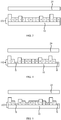
- FIG. 1 is a schematic diagram of a liquid crystal display panel of the conventional art.
- the color filter substrate 300 of the liquid crystal display panel of the conventional art is shown as FIG. 1 .
- red color resists R, green color resists G and blue color resists B are sequentially arranged.
- An upper substrate 40 is disposed oppositely to the lower base plate 30. Between the upper substrate 40 and the lower base plate 30, liquid crystal molecules are filled. Thicknesses of the three colors on the lower base plate 30 in the entire color filter substrate 300 of the conventional art are the same, and corresponding gaps d are the same.
- a relationship in wavelength among the red light, the green light and the blue light is ⁇ r > ⁇ g > ⁇ b
- a relationship of the variation amount in the transmittance of the red light, the green light and the blue light is ⁇ Tr ⁇ ⁇ Tg ⁇ ⁇ Tb . Therefore, from the center region to the edge region of the liquid crystal display panel the variation amount in the transmittance of the red light is smallest so that the brightness of the red light at the edge region of the liquid crystal display panel is highest such that when the user at the point "A" views the liquid crystal panel, the color at the edge region is shifted to red comparing to the center region so that a serious color-shift problem is existed.
- FIG. 2 is a schematic diagram of a liquid crystal display panel according to a first example not according to the invention.
- the liquid crystal display panel includes a color filter substrate 100, and the color filter substrate 100 includes a base plate 10 and multiple red color resists R, the blue color resists B and green color resists G on the base plate 10.
- thicknesses of the multiple red color resists R at an edge region of the base plate 10 is greater than thicknesses of the multiple color resists R at a center region of the base plate 10. That is, at the center region of the base plate 10, thicknesses of the red color resists R, the blue color resists B and the green color resists G are the same.
- the thicknesses of the blue color resists B and the green color resists G at the edge region are the same as the thicknesses of the blue color resists B and the green color resists G at the center region.
- the thicknesses of the red color resists R at the edge region are greater than the thicknesses of the red color resists R at the center region.
- the liquid crystal panel also includes another substrate 20 right opposite to the color filter substrate 100. The liquid crystal molecules are filled between the color filter substrate 100 and the another substrate 20.
- the thicknesses of the green color resists G and the blue color resists B are the same on the entire base plate 10.
- the thicknesses of the red color resists R at the center region is less than the thicknesses of the red color resists R at the edge region such that a cell gap of the red color resists at the center region is greater than a cell gap of the red color resists at the edge region so that the transmittance of the red light at the edge region is less than the transmittance of the red light at the center region in order to decrease the brightness of the red light at the edge region of the liquid crystal display panel.
- a variation amount in the transmittance of the red light is smaller than a variation amount in the transmittance of the red light in the conventional art such that a brightness ratio of the red light, the blue light and the green light is similar to a brightness ratio of the red light, the blue light and the green light at the center region in order to improve the red-shift phenomenon at the edge region of the liquid crystal panel.
- the base plate 10 of the color filter substrate 100 in the present example can be a glass base plate 10, or a TFT base plate 10. Because the color filter substrate 100 is used for filtering color in the liquid crystal panel so that the light pass through the liquid crystal display panel appears a corresponding color. According to the conventional manufacturing process, the base plate 10 of the color filter substrate 100 can be a glass base plate 10 or a TFT base plate 10.
- the color filter substrate 100 is further provided with a black matrix (not shown in the figure).
- the black matrix is disposed between two adjacent color resists.
- the black matrix is provided between the red color resists R and the green color resists G
- the black matrix is provided between the green color resists G and the blue color resists B.
- the black matrix is also provided.
- FIG. 3 is a schematic diagram of a liquid crystal display panel according to a second example not according to the invention.
- the present example is improved based on the liquid crystal display panel of the first example shown in FIG. 2 .
- each region includes multiple red color resists R, the blue color resists B and the green color resists G. Besides, width of each region can be the same or be different.
- the size of the liquid crystal panel is larger, when a user views a liquid crystal panel from a center region to an edge region, viewing angles of the user with respect to the liquid crystal panel are not changed suddenly, but gradually changed from the center region to the edge region of the liquid crystal panel.
- the base plate 10 is divided into multiple regions from the center to the edge such that the thicknesses of the red color resists R are as a gradient change from the center region to the edge region in the multiple regions so that a brightness ratio of the red light, the blue light and the green light of each region is similar to a brightness ratio of the red light, the blue light and the green light at the center region such that brightness ratios of the red light, the blue light and the green light on the entire liquid crystal panel tend to the same in order to improve the color shift problem of the liquid crystal display panel and increase the display quality.
- FIG. 4 is a schematic diagram of a liquid crystal display panel according to an embodiment of the present invention.
- the present embodiment is improved based on the liquid crystal display panel of the second embodiment. It can be understood that the arrangement of the thickness of the blue color resist B in the present embodiment can combine with the liquid crystal display panel of the first example shown in FIG. 2 .
- thicknesses of multiple blue color resists B disposed on the base plate 10 of the color filter substrate 102 located at the edge region is less than thicknesses of the multiple blue color resists B located at the center region.
- the wavelength of the green light is next only to a wavelength of the red light so that a variation amount in the transmittance of a green light is next only to a variation amount in the transmittance of the red light. Therefore, when a red-shift phenomenon at the edge region of the liquid crystal display panel is improved, a green-shift phenomenon is generated.
- a contribution of a brightness of the green color resist G is larger. If adopting a same method to increase the thicknesses of the green color resists G at the edge region of the base plate 10, the transmittance of the liquid crystal panel will decrease such that the brightness of the entire liquid crystal display panel is decreased so as to decrease the display quality. Accordingly, the method cannot be adopted.
- the thicknesses of the green color resists G at the edge region on the base plate 10 are equal to the thicknesses of the green color resists G at the center region so that for the entire liquid crystal display panel, the entire brightness will not decrease. Because a color of a liquid crystal display panel is decided by a brightness ratio of the red light, the green light and the blue light, the present embodiment reduces the thicknesses of the blue color resists B at the edge region of the base plate 10 so as to increase the transmittance of the blue light at the edge region of the liquid crystal display panel.
- the above method is equal to decrease the brightness of the green light at the edge region so as to improve the green-shift phenomenon at the edge region in order to increase the display quality.
- FIG. 5 is a schematic diagram of a liquid crystal display panel according to another embodiment of the present invention.
- the present embodiment is improved based on the liquid crystal display panel of the embodiment shown in FIG. 4 .
- the color filter substrate 103 of the liquid crystal display panel is dividing the base plate 10 into multiple regions from a center to an edge, and the thicknesses of the blue color resists B closer to the edge region of the base plate 10 is smaller. That is, in the multiple regions of the base plate 10, a thickness change of the blue color resists B on the base plate 10 is a gradient change. It can be understood that the arrangement of the thicknesses of the blue color resist B in the present embodiment can combine with the arrangement of the red color resist R in the liquid crystal display panel of the first example shown in FIG. 2 .
- each region when the base plate 10 is divided into multiple regions from the center to the edge, each region includes multiple red color resists R, multiple blue color resists B and multiple green color resists G. Besides, width of each region can be the same or be different.
- the arrangement of the blue color resists B in the present embodiment is similar to the gradient arrangement of the thicknesses of the red color resists R. Because the size of the liquid crystal panel is larger, when a user views a liquid crystal panel from a center region to an edge region, viewing angles of the user with respect to the liquid crystal panel are changed gradually from the center region to the edge region of the liquid crystal panel.
- the base plate 10 is divide into multiple regions from the center to the edge such that the thicknesses of the blue color resists B present a gradient arrangement from the center region to the edge region in the multiple regions so that a brightness ratio of the red light, the blue light and the green light of each region on the liquid crystal panel is similar to a brightness ratio of the red light, the blue light and the green light at the center region of the liquid crystal panel such that the brightness ratios of the red light, the blue light and the green light on the entire liquid crystal panel tend to be consistent in order to improve the color-shift problem of the liquid crystal display panel and increase the display quality.
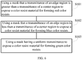
- FIG. 6 is a flow chart of a manufacturing method of a color filter substrate according to an embodiment of the present invention.
- an exposure process of the color filter substrate of the present invention includes following steps: S101: using a mask that a transmittance of an edge region is greater than a transmittance of a center region to expose a color resist material for forming red color resists.
- Coating a color resist material for forming red color resist on the base plate of the color filter substrate When exposing the color resist material for forming red color resist, using the mask that the transmittance of the edge region is greater than the transmittance of the center region to expose the color resist material for forming red color resists.
- the color resist material is a negative material
- an exposure intensity is larger such that a curing degree of the color resist material is more thorough. Accordingly, when exposing the color resist material for forming red color resist coated on the base plate, using the mask that the transmittance of the edge region is greater than the transmittance of the center region such that an exposure intensity of the color resist material at the edge region is greater than an exposure intensity of the color resist material at the center region such that a curing degree of the color resist material at the edge region is greater than a curing degree of the color resist material at the center region.
- a thickness of the red color resist at the edge region is greater than a thickness of the red color resist at the center region.
- the structure of the red color resists formed by the above method is as the structure of the red color resists R on the color filter substrate 100 in the liquid crystal display panel shown in FIG. 2 .
- the mask used for forming the color resist material for red color resists can be divided into multiple regions from a center to an edge such that an exposure intensity of the color resist material for forming red color resists closer to the center region of the substrate is smaller.
- the thicknesses of the red color resists closer to the center region of the base plate are smaller.
- the structure of the red color resists formed by the above method is the structure of the red color resists R on the color filter substrate 101 in the liquid crystal display panel shown in FIG. 3 .
- the structure of the blue color resist formed by the above method is as the structure of the blue color resists B on the color filter substrate 102 in the liquid crystal display panel shown in FIG. 4 .
- the mask used for forming the color material for forming blue color resists can be divided into multiple regions from a center to an edge.
- the transmittance of the region of the mask closer to the center of the mask is greater such that an exposure intensity of the color resist material for forming blue color resists closer to the center region of the base plate is greater.
- the thicknesses of the blue color resists closer to the center region of the base plate are greater.
- the structure of the blue color resists formed by the above method is the structure of the blue color resists B on the color filter substrate 103 in the liquid crystal display panel shown in FIG. 5 .
- the step 102 can also use a mask having an unchanged transmittance to expose the color resist material for forming blue color resists such that the thicknesses of the blue color resists on the color filter substrate are the same.
- the structure of the blue color resists formed by the above method is the structure of the blue color resist B on the color filter substrate 100 in the liquid crystal display panel as shown in FIG. 2 .
- step S101, the step S102 and the step S103 are respectively used for exposing the color resist materials for forming red color resists, blue color resists and green color resists in order to form the red color resists, the blue color resists and the green color resists, which does not have an order relationship. Therefore, among the step S101, the step S102 and the step 103, the execution sequence is not limited.
- the present invention further provides a liquid crystal display device.
- the liquid crystal display device includes a liquid crystal display panel and a driving circuit.
- the driving circuit is electrically connected to the liquid crystal display panel and through the driving circuit to drive the liquid crystal display panel.
- the liquid crystal display panel in the present embodiment can be anyone of the liquid crystal display panels shown in FIG. 4 to FIG. 5 .
- the thicknesses of the red color resists at the edge region is greater than the thicknesses of the red color resists at the center region of the base plate of the color filter substrate such that a cell gap corresponding to the red color resists at the center region of the liquid crystal panel is greater than a cell gap corresponding to the red color resists at the edge region. Accordingly, the color shift at the edge region of the liquid crystal display panel is compensated to improve a red-shift phenomenon generated at the edge region of the liquid crystal display panel so as to increase the display quality of the liquid crystal display panel.
Landscapes
- Physics & Mathematics (AREA)
- Nonlinear Science (AREA)
- Optics & Photonics (AREA)
- General Physics & Mathematics (AREA)
- Mathematical Physics (AREA)
- Crystallography & Structural Chemistry (AREA)
- Chemical & Material Sciences (AREA)
- Engineering & Computer Science (AREA)
- Manufacturing & Machinery (AREA)
- Microelectronics & Electronic Packaging (AREA)
- Optical Filters (AREA)
- Liquid Crystal (AREA)
- Devices For Indicating Variable Information By Combining Individual Elements (AREA)
Description
- The present invention relates to a display technology field, and more particularly to a color filter substrate, a liquid crystal panel, liquid crystal display device and a manufacturing method for the same.
- The conventional Vertical Alignment (VA) display mode has advantages of high contrast ratio and no friction alignment such that the VA display mode has become a normal display mode for a large size liquid crystal display panel.
- In the VA display mode, the liquid crystal molecules are stand vertically such that the VA display mode has a very high contrast ratio in a front side. However, when viewing at a side direction, the contrast ratio of the VA display mode is decreased obviously. The color of the picture easily generates a color shift. Specifically, when a user views at a center of the liquid crystal panel, an edge of the liquid display panel will generates a red-shift phenomenon.
-
US2016/341856 A1 discloses a color-film substrate and a liquid crystal device. The color-film includes a substrate body and a photo-resist layer on the substrate body. The photo-resist layer includes duplicated photo-resistors arranged in a sequence, and the photo-resist layer includes a first display area and a second display area arranged in a rim of the first display area. A thickness of the photo-resistors of the second display area is larger than a thickness of the photo-resistor of the first display area such that a transmission rate of the display panel corresponding to the second display area is smaller than the transmission rate of the display panel corresponding to the first display area. -
US2007/002218 A1 discloses a color filter substrate including a first color filter layer on a substrate, and a second color filter layer on the substrate, the first color filter layer having a thickness different from a thickness of the second color filter layer. -
CN 101498802 A provides a colored filter structure, the method and the application thereof; the colored filter structure comprises a substrate which is provided with a plurality of red, blue and green filtering cells, and the blue filtering cells are thinner than the red and the green filtering cells, thereby solving the problem that the distance among bright and dark neutral color spots is too far. - Accordingly, the present invention provides a color filter substrate, a liquid crystal display device and a manufacturing method of a color filter substrate and the color filter substrate of the present invention can improve the color-shift problem of the liquid crystal display display device.
- The invention is defined in the appended claims. In the present invention, a cell gap corresponding to the red color resists at the center region of the liquid crystal panel is greater than a cell gap corresponding to the red color resists at the edge region to reduce the difference of the red light of the transmittance at the center region and the transmittance at the edge region. Accordingly, a brightness ratio of the red light, the blue light and the green light at the edge region is similar to a brightness ratio of the red light, the blue light and the green light at the center region in order to improve a red-shift phenomenon generated at the edge region of the liquid crystal display panel so as to increase the display quality of the liquid crystal display panel.
-
-
FIG. 1 is a schematic diagram of a liquid crystal display panel according to the conventional art; -
FIG. 2 is a schematic diagram of a liquid crystal display panel according to a first example not according to the invention; -
FIG. 3 is a schematic diagram of a liquid crystal display panel according to a second example not according to the invention; -
FIG. 4 is a schematic diagram of a liquid crystal display panel according to an embodiment of the present invention; -
FIG. 5 is a schematic diagram of a liquid crystal display panel according to another embodiment of the present invention; and -
FIG. 6 is a flow chart of a manufacturing method for a color filter substrate according to an embodiment of the present invention. - In order to let the person skilled in the art to understood the the present invention better, the following will combine the figures and the specific embodiments to describe a color filter substrate, a liquid crystal panel, a liquid crystal display device and a manufacturing method for the same in detail. In the figures, a same numeral in the entire specification and figures represents a same element.
- A liquid crystal display panel generates different colors through controlling a brightness ratio of a red light, a green light and a blue light. Therefore, estimating a color-shift problem of a liquid crystal display panel in different viewing angles can be defined as estimating a problem of difference of brightness ratios of a red light, a green light and a blue light in different viewing angles of the liquid crystal display panel.
- In the VA display mode of the liquid crystal display panel, the transmittance of the three colors can refer to a following formula:

- In the formula, ϕ is an azimuth angle of liquid crystal molecules, Δnd is a factor of the change in transmittance, wherein, Δn is a difference of a normal light and an abnormal light caused by a birefringence property of liquid crystal molecules; d is a cell gap; λ is a wavelength of a light incident to the liquid crystal molecules. In the VA display mode, the azimuth angle of liquid crystal molecules is a fixed value. However, in different viewing angles, corresponding factors of the change in transmittance Δnd are different. Accordingly, in different viewing angles, the transmittance of the red light, the green light and the blue light are changed.
- With reference to
FIG. 1, FIG. 1 is a schematic diagram of a liquid crystal display panel of the conventional art. Thecolor filter substrate 300 of the liquid crystal display panel of the conventional art is shown asFIG. 1 . On alower base plate 30, red color resists R, green color resists G and blue color resists B are sequentially arranged. Anupper substrate 40 is disposed oppositely to thelower base plate 30. Between theupper substrate 40 and thelower base plate 30, liquid crystal molecules are filled. Thicknesses of the three colors on thelower base plate 30 in the entirecolor filter substrate 300 of the conventional art are the same, and corresponding gaps d are the same. - When a user located at point "A" views the liquid crystal panel, a front view is formed with respect to a center region of the liquid crystal display panel, edge regions are all side views, and changes of view angles are the same. At this time, the factors of the changes in the transmittance Δnd of the three colors are all decreased, and the variation amounts of the factors of the changes in the transmittance are the same. Assuming that the variation amount in the transmittance of the red light, the green light and the blue light are respectively ΔTr, ΔTg and ΔTb. Because a relationship in wavelength among the red light, the green light and the blue light is λr > λg > λb, according to the above formula, a relationship of the variation amount in the transmittance of the red light, the green light and the blue light is ΔTr < ΔTg < ΔTb. Therefore, from the center region to the edge region of the liquid crystal display panel the variation amount in the transmittance of the red light is smallest so that the brightness of the red light at the edge region of the liquid crystal display panel is highest such that when the user at the point "A" views the liquid crystal panel, the color at the edge region is shifted to red comparing to the center region so that a serious color-shift problem is existed.
- With reference to
FIG. 2, FIG. 2 is a schematic diagram of a liquid crystal display panel according to a first example not according to the invention. As shown inFIG. 2 , the liquid crystal display panel includes acolor filter substrate 100, and thecolor filter substrate 100 includes abase plate 10 and multiple red color resists R, the blue color resists B and green color resists G on thebase plate 10. Wherein, thicknesses of the multiple red color resists R at an edge region of thebase plate 10 is greater than thicknesses of the multiple color resists R at a center region of thebase plate 10. That is, at the center region of thebase plate 10, thicknesses of the red color resists R, the blue color resists B and the green color resists G are the same. However, the thicknesses of the blue color resists B and the green color resists G at the edge region are the same as the thicknesses of the blue color resists B and the green color resists G at the center region. The thicknesses of the red color resists R at the edge region are greater than the thicknesses of the red color resists R at the center region. Besides, the liquid crystal panel also includes anothersubstrate 20 right opposite to thecolor filter substrate 100. The liquid crystal molecules are filled between thecolor filter substrate 100 and theanother substrate 20. The thicknesses of the green color resists G and the blue color resists B are the same on theentire base plate 10. - In the present example, because the thicknesses of the red color resists R at the center region is less than the thicknesses of the red color resists R at the edge region such that a cell gap of the red color resists at the center region is greater than a cell gap of the red color resists at the edge region so that the transmittance of the red light at the edge region is less than the transmittance of the red light at the center region in order to decrease the brightness of the red light at the edge region of the liquid crystal display panel. When an user views the liquid crystal panel at a center location, from the center region to the edge region of the liquid crystal display panel, a variation amount in the transmittance of the red light is smaller than a variation amount in the transmittance of the red light in the conventional art such that a brightness ratio of the red light, the blue light and the green light is similar to a brightness ratio of the red light, the blue light and the green light at the center region in order to improve the red-shift phenomenon at the edge region of the liquid crystal panel.
- The
base plate 10 of thecolor filter substrate 100 in the present example can be aglass base plate 10, or aTFT base plate 10. Because thecolor filter substrate 100 is used for filtering color in the liquid crystal panel so that the light pass through the liquid crystal display panel appears a corresponding color. According to the conventional manufacturing process, thebase plate 10 of thecolor filter substrate 100 can be aglass base plate 10 or aTFT base plate 10. - In the present example, the
color filter substrate 100 is further provided with a black matrix (not shown in the figure). The black matrix is disposed between two adjacent color resists. For example, the black matrix is provided between the red color resists R and the green color resists G, the black matrix is provided between the green color resists G and the blue color resists B. Among the adjacent red color resists R, the adjacent green color resists G and adjacent blue color resists B, the black matrix is also provided. - Furthermore, with reference to
FIG. 3, and FIG. 3 is a schematic diagram of a liquid crystal display panel according to a second example not according to the invention. The present example is improved based on the liquid crystal display panel of the first example shown inFIG. 2 . - As shown in
FIG. 3 , in thecolor filter substrate 101 of the liquid crystal panel, dividing thebase plate 10 from a center to an edge into multiple regions. The thicknesses of the red color resists R are smaller when closer to the center of thebase plate 10. That is, in the multiple regions of thebase plate 10, the thicknesses of the red color resists are changed as a gradient change. At the center region of thebase plate 10, the thicknesses of the red color resists R, the blue color resists B and the green color resists G are the same. In an arbitrary one region of thebase plate 10, thicknesses of the blue color resists B and the green color resists G are unchanged. It can be understood that when thebase plate 10 is divided into multiple regions from the center to the edge, each region includes multiple red color resists R, the blue color resists B and the green color resists G. Besides, width of each region can be the same or be different. - Because the size of the liquid crystal panel is larger, when a user views a liquid crystal panel from a center region to an edge region, viewing angles of the user with respect to the liquid crystal panel are not changed suddenly, but gradually changed from the center region to the edge region of the liquid crystal panel. Accordingly, in the present example, the
base plate 10 is divided into multiple regions from the center to the edge such that the thicknesses of the red color resists R are as a gradient change from the center region to the edge region in the multiple regions so that a brightness ratio of the red light, the blue light and the green light of each region is similar to a brightness ratio of the red light, the blue light and the green light at the center region such that brightness ratios of the red light, the blue light and the green light on the entire liquid crystal panel tend to the same in order to improve the color shift problem of the liquid crystal display panel and increase the display quality. - With reference to
FIG. 4, and FIG. 4 is a schematic diagram of a liquid crystal display panel according to an embodiment of the present invention. The present embodiment is improved based on the liquid crystal display panel of the second embodiment. It can be understood that the arrangement of the thickness of the blue color resist B in the present embodiment can combine with the liquid crystal display panel of the first example shown inFIG. 2 . - As shown in
FIG. 4 , thicknesses of multiple blue color resists B disposed on thebase plate 10 of thecolor filter substrate 102 located at the edge region is less than thicknesses of the multiple blue color resists B located at the center region. - According to the analysis of the color shift, because the wavelength of the green light is next only to a wavelength of the red light so that a variation amount in the transmittance of a green light is next only to a variation amount in the transmittance of the red light. Therefore, when a red-shift phenomenon at the edge region of the liquid crystal display panel is improved, a green-shift phenomenon is generated. In a liquid crystal display panel, a contribution of a brightness of the green color resist G is larger. If adopting a same method to increase the thicknesses of the green color resists G at the edge region of the
base plate 10, the transmittance of the liquid crystal panel will decrease such that the brightness of the entire liquid crystal display panel is decreased so as to decrease the display quality. Accordingly, the method cannot be adopted. - In the present embodiment, the thicknesses of the green color resists G at the edge region on the
base plate 10 are equal to the thicknesses of the green color resists G at the center region so that for the entire liquid crystal display panel, the entire brightness will not decrease. Because a color of a liquid crystal display panel is decided by a brightness ratio of the red light, the green light and the blue light, the present embodiment reduces the thicknesses of the blue color resists B at the edge region of thebase plate 10 so as to increase the transmittance of the blue light at the edge region of the liquid crystal display panel. The above method is equal to decrease the brightness of the green light at the edge region so as to improve the green-shift phenomenon at the edge region in order to increase the display quality. - With reference to
FIG. 5, FIG. 5 is a schematic diagram of a liquid crystal display panel according to another embodiment of the present invention. The present embodiment is improved based on the liquid crystal display panel of the embodiment shown inFIG. 4 . - As shown in
FIG. 5 , thecolor filter substrate 103 of the liquid crystal display panel is dividing thebase plate 10 into multiple regions from a center to an edge, and the thicknesses of the blue color resists B closer to the edge region of thebase plate 10 is smaller. That is, in the multiple regions of thebase plate 10, a thickness change of the blue color resists B on thebase plate 10 is a gradient change. It can be understood that the arrangement of the thicknesses of the blue color resist B in the present embodiment can combine with the arrangement of the red color resist R in the liquid crystal display panel of the first example shown inFIG. 2 . - In the present, when the
base plate 10 is divided into multiple regions from the center to the edge, each region includes multiple red color resists R, multiple blue color resists B and multiple green color resists G. Besides, width of each region can be the same or be different. - The arrangement of the blue color resists B in the present embodiment is similar to the gradient arrangement of the thicknesses of the red color resists R. Because the size of the liquid crystal panel is larger, when a user views a liquid crystal panel from a center region to an edge region, viewing angles of the user with respect to the liquid crystal panel are changed gradually from the center region to the edge region of the liquid crystal panel. Accordingly, in the present embodiment, the
base plate 10 is divide into multiple regions from the center to the edge such that the thicknesses of the blue color resists B present a gradient arrangement from the center region to the edge region in the multiple regions so that a brightness ratio of the red light, the blue light and the green light of each region on the liquid crystal panel is similar to a brightness ratio of the red light, the blue light and the green light at the center region of the liquid crystal panel such that the brightness ratios of the red light, the blue light and the green light on the entire liquid crystal panel tend to be consistent in order to improve the color-shift problem of the liquid crystal display panel and increase the display quality. - With reference to
FIG. 6, and FIG. 6 is a flow chart of a manufacturing method of a color filter substrate according to an embodiment of the present invention. As shown inFIG. 6 , an exposure process of the color filter substrate of the present invention includes following steps:
S101: using a mask that a transmittance of an edge region is greater than a transmittance of a center region to expose a color resist material for forming red color resists. - Coating a color resist material for forming red color resist on the base plate of the color filter substrate. When exposing the color resist material for forming red color resist, using the mask that the transmittance of the edge region is greater than the transmittance of the center region to expose the color resist material for forming red color resists.
- Because the color resist material is a negative material, when a received exposure amount is more, an exposure intensity is larger such that a curing degree of the color resist material is more thorough. Accordingly, when exposing the color resist material for forming red color resist coated on the base plate, using the mask that the transmittance of the edge region is greater than the transmittance of the center region such that an exposure intensity of the color resist material at the edge region is greater than an exposure intensity of the color resist material at the center region such that a curing degree of the color resist material at the edge region is greater than a curing degree of the color resist material at the center region. Accordingly, when using a developing solution to the color resist material for forming red color resists, a thickness of the red color resist at the edge region is greater than a thickness of the red color resist at the center region. The structure of the red color resists formed by the above method is as the structure of the red color resists R on the
color filter substrate 100 in the liquid crystal display panel shown inFIG. 2 . - Besides, the mask used for forming the color resist material for red color resists can be divided into multiple regions from a center to an edge such that an exposure intensity of the color resist material for forming red color resists closer to the center region of the substrate is smaller. Correspondingly, the thicknesses of the red color resists closer to the center region of the base plate are smaller. The structure of the red color resists formed by the above method is the structure of the red color resists R on the
color filter substrate 101 in the liquid crystal display panel shown inFIG. 3 . - S102: using a mask that a transmittance of an edge region is less than a transmittance of a center region to expose a color resist material for forming blue color resists.
- Coating the color resist material for forming blue color resists on the base plate of the color filter substrate, when exposing the color resist material for forming blue color resist, using the mask that the transmittance of the edge region is less than the transmittance of the center region to expose the color resist material for forming blue color resist. The structure of the blue color resist formed by the above method is as the structure of the blue color resists B on the
color filter substrate 102 in the liquid crystal display panel shown inFIG. 4 . - Besides, the mask used for forming the color material for forming blue color resists can be divided into multiple regions from a center to an edge. The transmittance of the region of the mask closer to the center of the mask is greater such that an exposure intensity of the color resist material for forming blue color resists closer to the center region of the base plate is greater. Correspondingly, the thicknesses of the blue color resists closer to the center region of the base plate are greater. The structure of the blue color resists formed by the above method is the structure of the blue color resists B on the
color filter substrate 103 in the liquid crystal display panel shown inFIG. 5 . - Besides, the
step 102 can also use a mask having an unchanged transmittance to expose the color resist material for forming blue color resists such that the thicknesses of the blue color resists on the color filter substrate are the same. The structure of the blue color resists formed by the above method is the structure of the blue color resist B on thecolor filter substrate 100 in the liquid crystal display panel as shown inFIG. 2 . - S103: Using a mask having a uniform transmittance to expose a color resist material for forming green color resists.
- Because thicknesses of the green color resists are the same on the entire base plate of the color filter substrate, using the mask having the uniform transmittance to expose the color resist material for forming green color resists.
- It can be understood that the step S101, the step S102 and the step S103 are respectively used for exposing the color resist materials for forming red color resists, blue color resists and green color resists in order to form the red color resists, the blue color resists and the green color resists, which does not have an order relationship. Therefore, among the step S101, the step S102 and the
step 103, the execution sequence is not limited. - The present invention further provides a liquid crystal display device. The liquid crystal display device includes a liquid crystal display panel and a driving circuit. Wherein, the driving circuit is electrically connected to the liquid crystal display panel and through the driving circuit to drive the liquid crystal display panel. The liquid crystal display panel in the present embodiment can be anyone of the liquid crystal display panels shown in
FIG. 4 to FIG. 5 . - In the present invention, the thicknesses of the red color resists at the edge region is greater than the thicknesses of the red color resists at the center region of the base plate of the color filter substrate such that a cell gap corresponding to the red color resists at the center region of the liquid crystal panel is greater than a cell gap corresponding to the red color resists at the edge region. Accordingly, the color shift at the edge region of the liquid crystal display panel is compensated to improve a red-shift phenomenon generated at the edge region of the liquid crystal display panel so as to increase the display quality of the liquid crystal display panel.
- The above embodiments of the present invention are not used to limit the invention. The scope of the invention is defined by the appended claims.
Claims (14)
- A color filter substrate (100, 101, 102, 103), comprising:a base plate (10); andmultiple red color resist elements (R) disposed on the base plate (10);wherein, the thickness of the multiple red color resist elements (R) at an edge region of the base plate (10) is greater than the thickness of the multiple red color resist elements (R) at a center region of the base plate (10);characterized in that multiple blue color resist elements (B) are disposed on the base plate (10), and the thickness of the multiple blue color resist elements (B) at the edge region of the base plate (10) is less than the thickness of the multiple blue color resist elements (B) at the center region of the base plate (10).
- The color filter substrate (100, 101, 102, 103) according to claim 1, characterized in that the base plate (10) is divided into multiple regions from a center to an edge, the thicknesses of the multiple red color resist elements (R) on the multiple regions closer to the center of the base plate (10) are smaller than the thicknesses of the red color resist elements (R) on the multiple regions closer to the edge.
- The color filter substrate (100, 101, 102, 103) according to claim 2, characterized in that the thicknesses of the multiple blue color resist elements (B) on the multiple regions closer to the edge of the base plate (10) are smaller than the thicknesses of the blue color resist elements (B) on the multiple regions closer to the center.
- The color filter substrate (100, 101, 102, 103) according to claim 1, characterized in that multiple green color resist elements (G) are further provided on the base plate (10), the thickness of the multiple green color resist elements (G) at the edge region of the base plate (10) is equal to the thickness of the multiple green color resist elements (G) at the center region of the base plate (10).
- The color filter substrate (100, 101, 102, 103) according to claim 1, characterized in that the base plate (10) is a glass substrate or a TFT substrate.
- The color filter substrate (100, 101, 102, 103) according to claim 1, characterized in that the color filter substrate (100, 101, 102, 103) further comprises a black matrix disposed between two adjacent color resist elements.
- A manufacturing method of a color filter substrate (100, 101, 102, 103), according to claims 1-6 comprising steps of:in a process of exposing a color filter substrate (100, 101, 102, 103), using a mask that a transmittance of an edge region is greater than a transmittance of a center region to expose a color resist material for forming red color resist elements (R);and using another mask in which a transmittance of an edge region is less than a transmittance of a center region to expose a color resist material for forming blue color resist elements (B).
- The manufacturing method according to claim 7, characterized in that the mask is divided into multiple regions from a center to an edge, the transmittance of the multiple regions of the mask closer to the center of the mask is smaller than the transmittance of the multiple regions closer to the edge when exposing the color resist material for forming red color resist elements (R).
- The manufacturing method according to claim 7, characterized in that the other
mask is divided into multiple regions from a center to an edge, the transmittance of the multiple regions of the other mask closer to the center of the mask is greater than the transmittance of the multiple regions closer to the edge when exposing the color resist material for forming blue color resist elements (B). - A liquid crystal display device including a liquid crystal display panel and a driving circuit, wherein, the driving circuit is electrically connected to the liquid crystal display panel for driving the liquid crystal display panel, the liquid crystal display panel comprises the color filter substrate (100, 101, 102, 103) of claim 1, and wherein the base plate (10) is divided into multiple regions from a center to an edge, and thicknesses of the multiple red color resist elements (R) on the multiple regions closer to the center of the base plate (10) are smaller than the thicknesses of the red color resist elements (R) on the multiple regions closer to the edge.
- The liquid crystal display device according to claim 10, characterized in that thicknesses of the multiple blue color resist elements (B) on the multiple regions closer to the edge of the base plate (10) are smaller than the thicknesses of the blue color resist elements (B) on the multiple regions closer to the center.
- The liquid crystal display device according to claim 10, characterized in that multiple green color resist elements (G) are further provided on the base plate (10), the thickness of the multiple green color resist elements (G) at the edge region of the base plate (10) is equal to the thickness of the multiple green color resist elements (G) at the center region of the base plate (10).
- The liquid crystal display device according to claim 10, characterized in that the base plate (10) is a glass substrate or a TFT substrate.
- The liquid crystal display device according to claim 10, characterized in that the color filter substrate (100, 101, 102, 103) further comprises a black matrix disposed between two adjacent color resist elements.
Applications Claiming Priority (2)
| Application Number | Priority Date | Filing Date | Title |
|---|---|---|---|
| CN201611115694.9A CN106646992B (en) | 2016-12-07 | 2016-12-07 | A kind of color membrane substrates, liquid crystal display panel, liquid crystal display device and preparation method thereof |
| PCT/CN2017/000033 WO2018103169A1 (en) | 2016-12-07 | 2017-01-03 | Color film substrate, liquid crystal panel, liquid crystal display device and preparation method therefor |
Publications (3)
| Publication Number | Publication Date |
|---|---|
| EP3553596A1 EP3553596A1 (en) | 2019-10-16 |
| EP3553596A4 EP3553596A4 (en) | 2020-06-17 |
| EP3553596B1 true EP3553596B1 (en) | 2021-10-13 |
Family
ID=58819621
Family Applications (1)
| Application Number | Title | Priority Date | Filing Date |
|---|---|---|---|
| EP17878624.0A Active EP3553596B1 (en) | 2016-12-07 | 2017-01-03 | Colour filter substrate, liquid crystal display device and manufacturing method of a colour filter substrate |
Country Status (6)
| Country | Link |
|---|---|
| US (1) | US10725335B2 (en) |
| EP (1) | EP3553596B1 (en) |
| JP (1) | JP6915058B2 (en) |
| KR (1) | KR102202165B1 (en) |
| CN (1) | CN106646992B (en) |
| WO (1) | WO2018103169A1 (en) |
Families Citing this family (9)
| Publication number | Priority date | Publication date | Assignee | Title |
|---|---|---|---|---|
| CN106896569B (en) * | 2017-03-30 | 2019-03-15 | 武汉华星光电技术有限公司 | A kind of colored optical filtering substrates |
| CN107145006B (en) * | 2017-06-20 | 2020-10-02 | 惠科股份有限公司 | Array substrate and display panel |
| CN107153293B (en) * | 2017-06-20 | 2020-10-13 | 惠科股份有限公司 | Array substrate, display panel and display device |
| CN108281090B (en) * | 2018-01-17 | 2021-05-14 | 京东方科技集团股份有限公司 | Display substrate, display screen and electronic equipment |
| CN112666744B (en) * | 2020-12-29 | 2022-08-12 | 厦门天马微电子有限公司 | Color film substrate and manufacturing method thereof, display panel and display device |
| CN115220256A (en) * | 2021-04-21 | 2022-10-21 | 胡崇铭 | Vertically aligned liquid crystal display module |
| CN113485043A (en) * | 2021-07-26 | 2021-10-08 | 京东方科技集团股份有限公司 | Display panel and electronic equipment |
| CN114527596B (en) * | 2022-03-10 | 2023-10-03 | Tcl华星光电技术有限公司 | Display panels and mobile terminals |
| CN118330925B (en) * | 2024-04-29 | 2025-12-19 | 惠科股份有限公司 | Color film substrate and display panel |
Family Cites Families (16)
| Publication number | Priority date | Publication date | Assignee | Title |
|---|---|---|---|---|
| US4934791A (en) * | 1987-12-09 | 1990-06-19 | Matsushita Electric Industrial Co., Ltd. | Color filter |
| JPH05313006A (en) * | 1992-05-12 | 1993-11-26 | Fujitsu Ltd | Manufacture of color filter |
| JP2002098826A (en) * | 2000-09-26 | 2002-04-05 | Casio Comput Co Ltd | Manufacturing method of color filter |
| JP2003098517A (en) * | 2001-09-20 | 2003-04-03 | Seiko Epson Corp | Liquid crystal device, method of manufacturing the same, and electronic equipment |
| KR101089097B1 (en) * | 2004-06-28 | 2011-12-06 | 엘지디스플레이 주식회사 | Color filter substrate and liquid crystal display device using the same |
| KR20060015203A (en) * | 2004-08-13 | 2006-02-16 | 삼성전자주식회사 | Liquid crystal display panel and liquid crystal display device having same |
| KR101263496B1 (en) * | 2005-06-29 | 2013-05-13 | 엘지디스플레이 주식회사 | Color filter substructure and method for color filter substructure |
| JP2007271898A (en) * | 2006-03-31 | 2007-10-18 | Toray Ind Inc | Color filter for transflective liquid crystal display device, method for producing the same, and transflective liquid crystal display device using the same |
| KR101266740B1 (en) * | 2006-12-28 | 2013-05-28 | 엘지디스플레이 주식회사 | liquid crystal display device and method for fabricating the same |
| CN100445836C (en) * | 2007-02-08 | 2008-12-24 | 友达光电股份有限公司 | Liquid crystal display panel, array substrate and manufacturing method thereof |
| CN101498802A (en) * | 2008-02-01 | 2009-08-05 | 奇美电子股份有限公司 | Color filter structure, manufacturing method thereof and liquid crystal display device |
| KR101150192B1 (en) * | 2009-04-20 | 2012-06-12 | 삼성코닝정밀소재 주식회사 | Optical filter for display device and display device having the same |
| MY155206A (en) * | 2010-01-29 | 2015-09-30 | Sharp Kk | Liquid crystal display device |
| KR101799528B1 (en) * | 2010-05-25 | 2017-11-20 | 엘지디스플레이 주식회사 | Black matrix material for off-set printing apparatus and method of fabricating color filter substrate using the same |
| EP2606058B1 (en) * | 2010-07-21 | 2017-03-08 | Eastern Virginia Medical School | Peptide compounds to regulate the complement system |
| CN104777666B (en) * | 2015-04-30 | 2017-11-10 | 武汉华星光电技术有限公司 | A kind of color membrane substrates and liquid crystal display |
-
2016
- 2016-12-07 CN CN201611115694.9A patent/CN106646992B/en active Active
-
2017
- 2017-01-03 JP JP2019527290A patent/JP6915058B2/en active Active
- 2017-01-03 EP EP17878624.0A patent/EP3553596B1/en active Active
- 2017-01-03 KR KR1020197018586A patent/KR102202165B1/en active Active
- 2017-01-03 US US15/323,790 patent/US10725335B2/en active Active
- 2017-01-03 WO PCT/CN2017/000033 patent/WO2018103169A1/en not_active Ceased
Also Published As
| Publication number | Publication date |
|---|---|
| WO2018103169A1 (en) | 2018-06-14 |
| EP3553596A4 (en) | 2020-06-17 |
| EP3553596A1 (en) | 2019-10-16 |
| CN106646992A (en) | 2017-05-10 |
| US20180307094A1 (en) | 2018-10-25 |
| CN106646992B (en) | 2018-06-15 |
| US10725335B2 (en) | 2020-07-28 |
| JP2019536105A (en) | 2019-12-12 |
| JP6915058B2 (en) | 2021-08-04 |
| KR102202165B1 (en) | 2021-01-12 |
| KR20190085130A (en) | 2019-07-17 |
Similar Documents
| Publication | Publication Date | Title |
|---|---|---|
| EP3553596B1 (en) | Colour filter substrate, liquid crystal display device and manufacturing method of a colour filter substrate | |
| US11215865B2 (en) | Color filter substrate, manufacturing method thereof, and related devices | |
| US5753937A (en) | Color liquid crystal display device having a semitransparent layer on the inner surface of one of the substrates | |
| US20180335553A1 (en) | Method for manufacturing color filter substrate and method for manufacturing liquid crystal panel | |
| CN106019694A (en) | Color filter, LCD panel, LCD and color filter forming method | |
| US10365523B2 (en) | Display panel and manufacturing method based on BOA technology | |
| CN108089368A (en) | Color membrane substrates and preparation method, display device | |
| US9513413B2 (en) | Display device, color filter substrate and manufacturing method thereof | |
| US11372279B2 (en) | Display and method of manufacturing same | |
| CN208922014U (en) | Display panel | |
| US8482700B2 (en) | Panel for liquid crystal display device | |
| CN110361893B (en) | Reflective display panel, manufacturing method, control unit, and display device | |
| US11009740B2 (en) | Display panel and method for fabricating display panel | |
| US7349044B2 (en) | Liquid crystal display assembly having the interference filter disposed corresponding exclusively to the green region | |
| JP4260429B2 (en) | Color filter and liquid crystal display device | |
| CN105044967A (en) | Color filter substrate, manufacturing method of color filter substrate and liquid crystal display panel with color filter substrate | |
| US11966067B2 (en) | Display panel and manufacturing method therefor | |
| US11480718B2 (en) | Display panel and manufacturing method therefor | |
| JP2007225715A (en) | Manufacturing method of color filter for liquid crystal display device and color filter for liquid crystal display device | |
| JP3301218B2 (en) | Reflective color liquid crystal display | |
| US20080211999A1 (en) | Transflective Liquid Crystal Display Device | |
| JP2008261906A (en) | Color filter manufacturing method, color filter, and liquid crystal display device | |
| CN101324728A (en) | Liquid crystal display panel and method for manufacturing the same | |
| KR20090058990A (en) | Manufacturing method of liquid crystal display device | |
| US20170153477A1 (en) | Display Panel and Liquid Crystal Display |
Legal Events
| Date | Code | Title | Description |
|---|---|---|---|
| STAA | Information on the status of an ep patent application or granted ep patent |
Free format text: STATUS: THE INTERNATIONAL PUBLICATION HAS BEEN MADE |
|
| PUAI | Public reference made under article 153(3) epc to a published international application that has entered the european phase |
Free format text: ORIGINAL CODE: 0009012 |
|
| STAA | Information on the status of an ep patent application or granted ep patent |
Free format text: STATUS: REQUEST FOR EXAMINATION WAS MADE |
|
| 17P | Request for examination filed |
Effective date: 20190705 |
|
| AK | Designated contracting states |
Kind code of ref document: A1 Designated state(s): AL AT BE BG CH CY CZ DE DK EE ES FI FR GB GR HR HU IE IS IT LI LT LU LV MC MK MT NL NO PL PT RO RS SE SI SK SM TR |
|
| AX | Request for extension of the european patent |
Extension state: BA ME |
|
| DAV | Request for validation of the european patent (deleted) | ||
| DAX | Request for extension of the european patent (deleted) | ||
| A4 | Supplementary search report drawn up and despatched |
Effective date: 20200520 |
|
| RIC1 | Information provided on ipc code assigned before grant |
Ipc: G02F 1/1335 20060101AFI20200514BHEP |
|
| GRAP | Despatch of communication of intention to grant a patent |
Free format text: ORIGINAL CODE: EPIDOSNIGR1 |
|
| STAA | Information on the status of an ep patent application or granted ep patent |
Free format text: STATUS: GRANT OF PATENT IS INTENDED |
|
| INTG | Intention to grant announced |
Effective date: 20210507 |
|
| GRAS | Grant fee paid |
Free format text: ORIGINAL CODE: EPIDOSNIGR3 |
|
| GRAA | (expected) grant |
Free format text: ORIGINAL CODE: 0009210 |
|
| STAA | Information on the status of an ep patent application or granted ep patent |
Free format text: STATUS: THE PATENT HAS BEEN GRANTED |
|
| AK | Designated contracting states |
Kind code of ref document: B1 Designated state(s): AL AT BE BG CH CY CZ DE DK EE ES FI FR GB GR HR HU IE IS IT LI LT LU LV MC MK MT NL NO PL PT RO RS SE SI SK SM TR |
|
| REG | Reference to a national code |
Ref country code: GB Ref legal event code: FG4D |
|
| REG | Reference to a national code |
Ref country code: CH Ref legal event code: EP |
|
| REG | Reference to a national code |
Ref country code: DE Ref legal event code: R096 Ref document number: 602017047730 Country of ref document: DE |
|
| REG | Reference to a national code |
Ref country code: IE Ref legal event code: FG4D |
|
| REG | Reference to a national code |
Ref country code: AT Ref legal event code: REF Ref document number: 1438601 Country of ref document: AT Kind code of ref document: T Effective date: 20211115 |
|
| REG | Reference to a national code |
Ref country code: LT Ref legal event code: MG9D |
|
| REG | Reference to a national code |
Ref country code: NL Ref legal event code: MP Effective date: 20211013 |
|
| REG | Reference to a national code |
Ref country code: AT Ref legal event code: MK05 Ref document number: 1438601 Country of ref document: AT Kind code of ref document: T Effective date: 20211013 |
|
| PG25 | Lapsed in a contracting state [announced via postgrant information from national office to epo] |
Ref country code: RS Free format text: LAPSE BECAUSE OF FAILURE TO SUBMIT A TRANSLATION OF THE DESCRIPTION OR TO PAY THE FEE WITHIN THE PRESCRIBED TIME-LIMIT Effective date: 20211013 Ref country code: LT Free format text: LAPSE BECAUSE OF FAILURE TO SUBMIT A TRANSLATION OF THE DESCRIPTION OR TO PAY THE FEE WITHIN THE PRESCRIBED TIME-LIMIT Effective date: 20211013 Ref country code: FI Free format text: LAPSE BECAUSE OF FAILURE TO SUBMIT A TRANSLATION OF THE DESCRIPTION OR TO PAY THE FEE WITHIN THE PRESCRIBED TIME-LIMIT Effective date: 20211013 Ref country code: BG Free format text: LAPSE BECAUSE OF FAILURE TO SUBMIT A TRANSLATION OF THE DESCRIPTION OR TO PAY THE FEE WITHIN THE PRESCRIBED TIME-LIMIT Effective date: 20220113 Ref country code: AT Free format text: LAPSE BECAUSE OF FAILURE TO SUBMIT A TRANSLATION OF THE DESCRIPTION OR TO PAY THE FEE WITHIN THE PRESCRIBED TIME-LIMIT Effective date: 20211013 |
|
| PG25 | Lapsed in a contracting state [announced via postgrant information from national office to epo] |
Ref country code: IS Free format text: LAPSE BECAUSE OF FAILURE TO SUBMIT A TRANSLATION OF THE DESCRIPTION OR TO PAY THE FEE WITHIN THE PRESCRIBED TIME-LIMIT Effective date: 20220213 Ref country code: SE Free format text: LAPSE BECAUSE OF FAILURE TO SUBMIT A TRANSLATION OF THE DESCRIPTION OR TO PAY THE FEE WITHIN THE PRESCRIBED TIME-LIMIT Effective date: 20211013 Ref country code: PT Free format text: LAPSE BECAUSE OF FAILURE TO SUBMIT A TRANSLATION OF THE DESCRIPTION OR TO PAY THE FEE WITHIN THE PRESCRIBED TIME-LIMIT Effective date: 20220214 Ref country code: PL Free format text: LAPSE BECAUSE OF FAILURE TO SUBMIT A TRANSLATION OF THE DESCRIPTION OR TO PAY THE FEE WITHIN THE PRESCRIBED TIME-LIMIT Effective date: 20211013 Ref country code: NO Free format text: LAPSE BECAUSE OF FAILURE TO SUBMIT A TRANSLATION OF THE DESCRIPTION OR TO PAY THE FEE WITHIN THE PRESCRIBED TIME-LIMIT Effective date: 20220113 Ref country code: NL Free format text: LAPSE BECAUSE OF FAILURE TO SUBMIT A TRANSLATION OF THE DESCRIPTION OR TO PAY THE FEE WITHIN THE PRESCRIBED TIME-LIMIT Effective date: 20211013 Ref country code: LV Free format text: LAPSE BECAUSE OF FAILURE TO SUBMIT A TRANSLATION OF THE DESCRIPTION OR TO PAY THE FEE WITHIN THE PRESCRIBED TIME-LIMIT Effective date: 20211013 Ref country code: HR Free format text: LAPSE BECAUSE OF FAILURE TO SUBMIT A TRANSLATION OF THE DESCRIPTION OR TO PAY THE FEE WITHIN THE PRESCRIBED TIME-LIMIT Effective date: 20211013 Ref country code: GR Free format text: LAPSE BECAUSE OF FAILURE TO SUBMIT A TRANSLATION OF THE DESCRIPTION OR TO PAY THE FEE WITHIN THE PRESCRIBED TIME-LIMIT Effective date: 20220114 Ref country code: ES Free format text: LAPSE BECAUSE OF FAILURE TO SUBMIT A TRANSLATION OF THE DESCRIPTION OR TO PAY THE FEE WITHIN THE PRESCRIBED TIME-LIMIT Effective date: 20211013 |
|
| REG | Reference to a national code |
Ref country code: DE Ref legal event code: R097 Ref document number: 602017047730 Country of ref document: DE |
|
| PG25 | Lapsed in a contracting state [announced via postgrant information from national office to epo] |
Ref country code: SM Free format text: LAPSE BECAUSE OF FAILURE TO SUBMIT A TRANSLATION OF THE DESCRIPTION OR TO PAY THE FEE WITHIN THE PRESCRIBED TIME-LIMIT Effective date: 20211013 Ref country code: SK Free format text: LAPSE BECAUSE OF FAILURE TO SUBMIT A TRANSLATION OF THE DESCRIPTION OR TO PAY THE FEE WITHIN THE PRESCRIBED TIME-LIMIT Effective date: 20211013 Ref country code: RO Free format text: LAPSE BECAUSE OF FAILURE TO SUBMIT A TRANSLATION OF THE DESCRIPTION OR TO PAY THE FEE WITHIN THE PRESCRIBED TIME-LIMIT Effective date: 20211013 Ref country code: EE Free format text: LAPSE BECAUSE OF FAILURE TO SUBMIT A TRANSLATION OF THE DESCRIPTION OR TO PAY THE FEE WITHIN THE PRESCRIBED TIME-LIMIT Effective date: 20211013 Ref country code: DK Free format text: LAPSE BECAUSE OF FAILURE TO SUBMIT A TRANSLATION OF THE DESCRIPTION OR TO PAY THE FEE WITHIN THE PRESCRIBED TIME-LIMIT Effective date: 20211013 Ref country code: CZ Free format text: LAPSE BECAUSE OF FAILURE TO SUBMIT A TRANSLATION OF THE DESCRIPTION OR TO PAY THE FEE WITHIN THE PRESCRIBED TIME-LIMIT Effective date: 20211013 |
|
| PLBE | No opposition filed within time limit |
Free format text: ORIGINAL CODE: 0009261 |
|
| STAA | Information on the status of an ep patent application or granted ep patent |
Free format text: STATUS: NO OPPOSITION FILED WITHIN TIME LIMIT |
|
| PG25 | Lapsed in a contracting state [announced via postgrant information from national office to epo] |
Ref country code: MC Free format text: LAPSE BECAUSE OF FAILURE TO SUBMIT A TRANSLATION OF THE DESCRIPTION OR TO PAY THE FEE WITHIN THE PRESCRIBED TIME-LIMIT Effective date: 20211013 |
|
| REG | Reference to a national code |
Ref country code: CH Ref legal event code: PL |
|
| 26N | No opposition filed |
Effective date: 20220714 |
|
| GBPC | Gb: european patent ceased through non-payment of renewal fee |
Effective date: 20220113 |
|
| REG | Reference to a national code |
Ref country code: BE Ref legal event code: MM Effective date: 20220131 |
|
| PG25 | Lapsed in a contracting state [announced via postgrant information from national office to epo] |
Ref country code: LU Free format text: LAPSE BECAUSE OF NON-PAYMENT OF DUE FEES Effective date: 20220103 Ref country code: GB Free format text: LAPSE BECAUSE OF NON-PAYMENT OF DUE FEES Effective date: 20220113 Ref country code: AL Free format text: LAPSE BECAUSE OF FAILURE TO SUBMIT A TRANSLATION OF THE DESCRIPTION OR TO PAY THE FEE WITHIN THE PRESCRIBED TIME-LIMIT Effective date: 20211013 |
|
| PG25 | Lapsed in a contracting state [announced via postgrant information from national office to epo] |
Ref country code: SI Free format text: LAPSE BECAUSE OF FAILURE TO SUBMIT A TRANSLATION OF THE DESCRIPTION OR TO PAY THE FEE WITHIN THE PRESCRIBED TIME-LIMIT Effective date: 20211013 Ref country code: FR Free format text: LAPSE BECAUSE OF NON-PAYMENT OF DUE FEES Effective date: 20220131 Ref country code: BE Free format text: LAPSE BECAUSE OF NON-PAYMENT OF DUE FEES Effective date: 20220131 |
|
| PG25 | Lapsed in a contracting state [announced via postgrant information from national office to epo] |
Ref country code: LI Free format text: LAPSE BECAUSE OF NON-PAYMENT OF DUE FEES Effective date: 20220131 Ref country code: CH Free format text: LAPSE BECAUSE OF NON-PAYMENT OF DUE FEES Effective date: 20220131 |
|
| PG25 | Lapsed in a contracting state [announced via postgrant information from national office to epo] |
Ref country code: IE Free format text: LAPSE BECAUSE OF NON-PAYMENT OF DUE FEES Effective date: 20220103 |
|
| PG25 | Lapsed in a contracting state [announced via postgrant information from national office to epo] |
Ref country code: IT Free format text: LAPSE BECAUSE OF FAILURE TO SUBMIT A TRANSLATION OF THE DESCRIPTION OR TO PAY THE FEE WITHIN THE PRESCRIBED TIME-LIMIT Effective date: 20211013 |
|
| P01 | Opt-out of the competence of the unified patent court (upc) registered |
Effective date: 20230530 |
|
| PG25 | Lapsed in a contracting state [announced via postgrant information from national office to epo] |
Ref country code: MK Free format text: LAPSE BECAUSE OF FAILURE TO SUBMIT A TRANSLATION OF THE DESCRIPTION OR TO PAY THE FEE WITHIN THE PRESCRIBED TIME-LIMIT Effective date: 20211013 Ref country code: CY Free format text: LAPSE BECAUSE OF FAILURE TO SUBMIT A TRANSLATION OF THE DESCRIPTION OR TO PAY THE FEE WITHIN THE PRESCRIBED TIME-LIMIT Effective date: 20211013 |
|
| PG25 | Lapsed in a contracting state [announced via postgrant information from national office to epo] |
Ref country code: HU Free format text: LAPSE BECAUSE OF FAILURE TO SUBMIT A TRANSLATION OF THE DESCRIPTION OR TO PAY THE FEE WITHIN THE PRESCRIBED TIME-LIMIT; INVALID AB INITIO Effective date: 20170103 |
|
| PG25 | Lapsed in a contracting state [announced via postgrant information from national office to epo] |
Ref country code: MT Free format text: LAPSE BECAUSE OF FAILURE TO SUBMIT A TRANSLATION OF THE DESCRIPTION OR TO PAY THE FEE WITHIN THE PRESCRIBED TIME-LIMIT Effective date: 20211013 |
|
| PG25 | Lapsed in a contracting state [announced via postgrant information from national office to epo] |
Ref country code: TR Free format text: LAPSE BECAUSE OF FAILURE TO SUBMIT A TRANSLATION OF THE DESCRIPTION OR TO PAY THE FEE WITHIN THE PRESCRIBED TIME-LIMIT Effective date: 20211013 |
|
| PGFP | Annual fee paid to national office [announced via postgrant information from national office to epo] |
Ref country code: DE Payment date: 20260121 Year of fee payment: 10 |