EP3553577A1 - Optische vorrichtungsanordnung mit einer auf einer halterung befestigten einmodigen optischen vorrichtung und verfahren zur befestigung davon - Google Patents
Optische vorrichtungsanordnung mit einer auf einer halterung befestigten einmodigen optischen vorrichtung und verfahren zur befestigung davon Download PDFInfo
- Publication number
- EP3553577A1 EP3553577A1 EP18305423.8A EP18305423A EP3553577A1 EP 3553577 A1 EP3553577 A1 EP 3553577A1 EP 18305423 A EP18305423 A EP 18305423A EP 3553577 A1 EP3553577 A1 EP 3553577A1
- Authority
- EP
- European Patent Office
- Prior art keywords
- optical device
- assembly
- walls
- locating
- bonding element
- Prior art date
- Legal status (The legal status is an assumption and is not a legal conclusion. Google has not performed a legal analysis and makes no representation as to the accuracy of the status listed.)
- Granted
Links
Images


Classifications
-
- G—PHYSICS
- G02—OPTICS
- G02B—OPTICAL ELEMENTS, SYSTEMS OR APPARATUS
- G02B6/00—Light guides; Structural details of arrangements comprising light guides and other optical elements, e.g. couplings
- G02B6/24—Coupling light guides
- G02B6/42—Coupling light guides with opto-electronic elements
- G02B6/4201—Packages, e.g. shape, construction, internal or external details
- G02B6/4219—Mechanical fixtures for holding or positioning the elements relative to each other in the couplings; Alignment methods for the elements, e.g. measuring or observing methods especially used therefor
-
- G—PHYSICS
- G02—OPTICS
- G02B—OPTICAL ELEMENTS, SYSTEMS OR APPARATUS
- G02B6/00—Light guides; Structural details of arrangements comprising light guides and other optical elements, e.g. couplings
- G02B6/24—Coupling light guides
- G02B6/36—Mechanical coupling means
- G02B6/3628—Mechanical coupling means for mounting fibres to supporting carriers
- G02B6/3632—Mechanical coupling means for mounting fibres to supporting carriers characterised by the cross-sectional shape of the mechanical coupling means
- G02B6/3636—Mechanical coupling means for mounting fibres to supporting carriers characterised by the cross-sectional shape of the mechanical coupling means the mechanical coupling means being grooves
- G02B6/364—Mechanical coupling means for mounting fibres to supporting carriers characterised by the cross-sectional shape of the mechanical coupling means the mechanical coupling means being grooves inverted grooves, e.g. dovetails
-
- G—PHYSICS
- G02—OPTICS
- G02B—OPTICAL ELEMENTS, SYSTEMS OR APPARATUS
- G02B6/00—Light guides; Structural details of arrangements comprising light guides and other optical elements, e.g. couplings
- G02B6/24—Coupling light guides
- G02B6/42—Coupling light guides with opto-electronic elements
- G02B6/4201—Packages, e.g. shape, construction, internal or external details
- G02B6/4219—Mechanical fixtures for holding or positioning the elements relative to each other in the couplings; Alignment methods for the elements, e.g. measuring or observing methods especially used therefor
- G02B6/4236—Fixing or mounting methods of the aligned elements
- G02B6/4239—Adhesive bonding; Encapsulation with polymer material
-
- G—PHYSICS
- G02—OPTICS
- G02B—OPTICAL ELEMENTS, SYSTEMS OR APPARATUS
- G02B6/00—Light guides; Structural details of arrangements comprising light guides and other optical elements, e.g. couplings
- G02B6/24—Coupling light guides
- G02B6/42—Coupling light guides with opto-electronic elements
- G02B6/4201—Packages, e.g. shape, construction, internal or external details
- G02B6/4219—Mechanical fixtures for holding or positioning the elements relative to each other in the couplings; Alignment methods for the elements, e.g. measuring or observing methods especially used therefor
- G02B6/4236—Fixing or mounting methods of the aligned elements
- G02B6/424—Mounting of the optical light guide
- G02B6/4243—Mounting of the optical light guide into a groove
-
- G—PHYSICS
- G02—OPTICS
- G02B—OPTICAL ELEMENTS, SYSTEMS OR APPARATUS
- G02B6/00—Light guides; Structural details of arrangements comprising light guides and other optical elements, e.g. couplings
- G02B6/24—Coupling light guides
- G02B6/42—Coupling light guides with opto-electronic elements
- G02B6/4201—Packages, e.g. shape, construction, internal or external details
- G02B6/4219—Mechanical fixtures for holding or positioning the elements relative to each other in the couplings; Alignment methods for the elements, e.g. measuring or observing methods especially used therefor
- G02B6/4236—Fixing or mounting methods of the aligned elements
- G02B6/4245—Mounting of the opto-electronic elements
-
- G—PHYSICS
- G02—OPTICS
- G02B—OPTICAL ELEMENTS, SYSTEMS OR APPARATUS
- G02B6/00—Light guides; Structural details of arrangements comprising light guides and other optical elements, e.g. couplings
- G02B6/24—Coupling light guides
- G02B6/36—Mechanical coupling means
- G02B6/3628—Mechanical coupling means for mounting fibres to supporting carriers
- G02B6/3632—Mechanical coupling means for mounting fibres to supporting carriers characterised by the cross-sectional shape of the mechanical coupling means
Definitions
- Various example embodiments relate to the optical assembly of single-mode devices (active or passive) like lasers, optical amplifiers, modulators (amplitude and/or phase), passive waveguides as well single-mode fibers or optical lenses. More precisely, the active devices are optoelectronic devices mainly based on Group III-V materials used for telecom/datacom applications.
- a very low noise laser cavity can be obtained by the hybrid integration of two optical devices, each of which are "Best In-Class" for their features.
- the first device is a Semi-conductor Optical Amplifier (SOA) to provide gain.
- SOA Semi-conductor Optical Amplifier
- Group III-V devices are (one of) the key leaders for ultra-wide optical bandwidth SOA at 100 nm.
- the second device is a low loss, long optical waveguide integrating a filter to ensure the low noise, single frequency and tuning of the laser beam.
- Dimensions of the SOA chip and of the waveguide chip are typically 2 to 5 mm x 0.5 mm x 0.12 mm and 4 to 10 mm x 5 mm x 1 mm (length x width x thickness) respectively.
- the size and the geometry of the chips (of rectangular shap versus the size and the geometry of the fiber (having typically a diameter of 250 ⁇ m) makes assembly difficult, and that assembly is made more difficult by the need to preserve the top and/or bottom surfaces of the chips for electrical contact.
- Various example embodiments propose an optical device assembly comprising a single-mode optical device secured on a holder and a method of securing the same to solve the prior art drawbacks.
- the optical device assembly comprises :
- the optical device may be secured to the walls of the holder so that the longitudinal axis of symmetry of the housing approximately coincides with the optical axis of the optical device.
- the optical device assembly prevents any parasitic movement during the solidification of the bonding element (notably a glue) during the securing of the optical device to the holder.
- the bonding element notably a glue
- optical device usable alone or in combination (provided that there is no conflict between the different elements) are:
- the method of securing a single-mode optical device on a holder provides the following steps:
- the single-mode optical device, the holder and the bonding elements are as defined above.
- the optical device may be positioned so that the longitudinal axis of symmetry of the housing coincides approximately with the optical axis of the optical device.
- Figures 1 to 3 illustrate a first embodiment of an assembly device 1 comprising a rectangular waveguide chip 2 secured to a U-shaped holder 3.
- the waveguide chip includes a single-mode optical waveguide illustrated by figure 3 .
- Figures 4a and 4b illustrate a second embodiment of an assembly device 1 comprising a rectangular 2 optical element which can be a waveguide chip secured to a U-shaped holder 3.
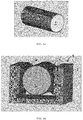
- Figures 5a and 5b illustrate a third embodiment of an assembly device 1 comprising a cylindrical element which can be, for example, a fiber ferule or an optical lens 2 secured to a U-shaped holder 3.
- a cylindrical element which can be, for example, a fiber ferule or an optical lens 2 secured to a U-shaped holder 3.
- Figures 1 to 5b show that each embodiment of assembly device 1 comprises a single-mode optical device 2 secured to a U-shaped holder 3.
- the optical device 2 is a rectangular waveguide chip 2, while in the embodiment shown in Figures 5a and 5b , the optical device 2 is a fibre ferule.
- the holder 3 comprises a substrate 31 with an upper surface 311 and two separated walls 32, fastened on the substrate 31 so that the holder 3 has a U-shape.
- the substrate 31 defines a housing 33 having a longitudinal axis of symmetry 34 and dimensions adapted to receive the optical device 2.
- Each wall 32 of the holder 3 comprises a locating portion 322 for allowing a bonding element 4 to flow along this locating portion 322 and at least one binding preventing portion 323 for preventing the flowing of said bonding element 4 along the binding preventing portion 323.
- a binding preventing portion 323 is located on a wall 32 between the substrate 31 and the locating portion 322.
- each wall 32 The locating portions 322 of each wall 32 are disposed facing each other symmetrically with respect to the longitudinal axis 34 of the housing 33.
- a bonding element 4 covers the locating portions of said walls 32.
- the optical device 2 is secured to the walls 32 of the holder 3 so that the longitudinal axis of symmetry 34 of the housing 33 coincides with the optical axis 21 of the optical device, while the binding preventing portions 323 of the walls 32 and the zone between the substrate 31 and the waveguide 2 are free of bonding element 4.
- each locating portion 322 of the walls 32 is constituted, in the same manner as the embodiment of figure 1 , by a protruding portion of the wall 32 connected to each of said walls by two faces respectively, each face defining an angle ⁇ with said wall that is strictly greater than 0° and strictly less than 180°, preferably of about 90°.
- the angle ⁇ is 90°
- it is about 30 to 45° ( figure 2b ) and about 120° ( figure 2d ) respectively.
- each side of the waveguide chip 2 there are lateral gaps filled with the bonding element 4.
- the dimensions of these gaps are typically in the range of 10 to 50 ⁇ m in the horizontal direction.
- a deeper gap is designed between the bottom of the waveguide 2 and the upper surface of the substrate, to ensure that no bonding element 4 (for instance glue) is flowing in-between.
- This embodiment allows the localization of the bonding element 4, for instance glue.
- the flowing of the bonding element 4 is stopped and controlled to achieve a vertical symmetry in the gluing between the holder 3 and the waveguide 4.
- this design of the holder 3 avoids the filling of the gap in-between the bottom of the waveguide 2 and the holder 3.
- the locating portions 322 of the walls 32 are surfaces capable of being wetted by the bonding element 4 while the binding preventing portions 323 cannot be wetted by said bonding element 4.
- This embodiment also allows the localization of the bonding element 4. In this configuration, the flowing of the bonding element 4 is stopped and controlled to achieve a vertical symmetry in the gluing between the holder 3 and the waveguide 4.
- FIG. 4b corresponds to the realization mode of figure 4a
- the upper and lower side views of figure 4b respectively correspond to embodiments in which the locating portion is centered and surrounded below and above by binding preventing portions.
- the upper view differs from the lower view in that the locating portion is also surrounded on the sides by binding preventing portions.
- each locating portion 322 of the walls 32 is constituted by a protruding portion, each defining an angle ⁇ with the walls that is strictly greater than 0° and strictly less than 180°, and preferably of about 90°.
- FIG 6 a flowchart of an embodiment of a method 500 of securing a single-mode optical device (for instance a waveguide chip) on a holder is shown.
- the method 500 may be implemented by a manufacturer when an optical device assembly 1 comprising a single-mode optical device 2 secured to a holder 3 is in a process of being manufactured.
- a holder 3 comprising a substrate 31 with an upper surface 311 and two separated walls 32 is provided.
- Each wall 32 is attached to the upper surface 311 of the substrate 31 at one of their ends, so as to define a housing 33 having a longitudinal axis of symmetry.
- the dimensions of this housing 33 are adapted to receive a single-mode optical device 2 such a waveguide (for instance the fiber ferule of figure 5a and 5b or the rectangular waveguide of figures 1 to 4b ).
- Figures 1 to 5 show that each wall 32 has a locating portion 322 for allowing a bonding element 4 (such as glue) to flow along the locating portion 322 and at least one binding preventing portion 323 for preventing the flowing of said bonding element 4 along the binding preventing portion.
- the binding preventing portion 323 is located between the substrate 31 and the locating portion 322, the locating portions of each wall being disposed facing each other symmetrically with respect to the longitudinal axis of the housing 33.
- the optical device 2 is positioned in the housing 33 so that it is not in contact (gaps) with the walls 32 of the holder 33 and with the upper surface 311 of the substrate 31, and the longitudinal axis of symmetry of the housing 33 coincides as much as possible with the optical axis 21 of the optical device 2, as in the embodiments illustrated in figures 1 to 5b .
- a bonding element 4 (such as an ultraviolet-setting adhesive or a thermosetting resin, notably an epoxy-resin) is dispensed in the gaps between the locating portions 322 of the walls 32 and the optical device 2.
- the bonding element 4 is solidified so as to fasten the optical device 2 on the holder 3.
- the optical device 2 can be inserted inside without being in contact with any walls of the holder 3, while ensuring that its optical axis 21 coincides as much as possible with the longitudinal axis of symmetry of the housing 33. Otherwise, the shrinkage of the bonding element 4 during solidification would induce a dramatic misalignment in the lateral direction during the assembling.
- the optical device 2 may be arranged symmetrically with respect to the plane passing by the middle of each locating portion 322. Otherwise, the shrinkage of the bonding element 4 during solidification would induce a dramatic miss alignment during the assembling as the vertical direction (perpendicular to the optical axis) is more sensitive than the lateral direction to the coupling efficiency in most of the cases. Note that this vertical shrinkage cannot be balanced by symmetry gluing on the top of the optical device because on one hand the top has to be prevented of gluing for future electrical contacts and on the other hand this side of the optical device 2 is used for its manipulation using a proper tool.
Landscapes
- Physics & Mathematics (AREA)
- General Physics & Mathematics (AREA)
- Optics & Photonics (AREA)
- Optical Couplings Of Light Guides (AREA)
Priority Applications (1)
| Application Number | Priority Date | Filing Date | Title |
|---|---|---|---|
| EP18305423.8A EP3553577B1 (de) | 2018-04-10 | 2018-04-10 | Optische vorrichtungsanordnung mit einer auf einer halterung befestigten einmodigen optischen vorrichtung und verfahren zur befestigung davon |
Applications Claiming Priority (1)
| Application Number | Priority Date | Filing Date | Title |
|---|---|---|---|
| EP18305423.8A EP3553577B1 (de) | 2018-04-10 | 2018-04-10 | Optische vorrichtungsanordnung mit einer auf einer halterung befestigten einmodigen optischen vorrichtung und verfahren zur befestigung davon |
Publications (2)
| Publication Number | Publication Date |
|---|---|
| EP3553577A1 true EP3553577A1 (de) | 2019-10-16 |
| EP3553577B1 EP3553577B1 (de) | 2021-07-28 |
Family
ID=62063469
Family Applications (1)
| Application Number | Title | Priority Date | Filing Date |
|---|---|---|---|
| EP18305423.8A Active EP3553577B1 (de) | 2018-04-10 | 2018-04-10 | Optische vorrichtungsanordnung mit einer auf einer halterung befestigten einmodigen optischen vorrichtung und verfahren zur befestigung davon |
Country Status (1)
| Country | Link |
|---|---|
| EP (1) | EP3553577B1 (de) |
Citations (2)
| Publication number | Priority date | Publication date | Assignee | Title |
|---|---|---|---|---|
| US5239601A (en) * | 1990-03-01 | 1993-08-24 | Commissariat A L'energie Atomique | Connection process between an optical fibre and an optical microguide |
| US20130004167A1 (en) * | 2011-07-01 | 2013-01-03 | Kim Brian H | Optical frame attached with alignment features microfabrictated in die |
-
2018
- 2018-04-10 EP EP18305423.8A patent/EP3553577B1/de active Active
Patent Citations (2)
| Publication number | Priority date | Publication date | Assignee | Title |
|---|---|---|---|---|
| US5239601A (en) * | 1990-03-01 | 1993-08-24 | Commissariat A L'energie Atomique | Connection process between an optical fibre and an optical microguide |
| US20130004167A1 (en) * | 2011-07-01 | 2013-01-03 | Kim Brian H | Optical frame attached with alignment features microfabrictated in die |
Also Published As
| Publication number | Publication date |
|---|---|
| EP3553577B1 (de) | 2021-07-28 |
Similar Documents
| Publication | Publication Date | Title |
|---|---|---|
| US12276847B2 (en) | Optical connecting component and optical connecting structure | |
| US10082625B2 (en) | Optical component with angled-facet waveguide | |
| US10782474B2 (en) | Detachable optical connectors for optical chips comprising a connector support and methods of fabricating the same | |
| US10591694B2 (en) | Photonic chip having a monolithically integrated reflector unit and method of manufacturing a reflector unit | |
| TWI675229B (zh) | 包含矽光晶片和耦合器晶片的光學模組 | |
| US11415761B2 (en) | Optical fiber guide component, optical connection structure and method for producing same | |
| US7223025B2 (en) | Packaging for a fiber-coupled optical device | |
| US6848839B2 (en) | Methods and devices for coupling optoelectronic packages | |
| US12158611B2 (en) | Optical fiber guide structure and optical fiber connecting structure | |
| US12061361B2 (en) | Optical fiber connecting structure | |
| O’Brien et al. | Packaging of silicon photonic devices | |
| EP3553577B1 (de) | Optische vorrichtungsanordnung mit einer auf einer halterung befestigten einmodigen optischen vorrichtung und verfahren zur befestigung davon | |
| US9897760B2 (en) | Optical device, optical modulator, and method for manufacturing optical device | |
| US12111500B2 (en) | Optical fiber guide structure and optical fiber connecting structure | |
| Bourhis | Fiber-to-waveguide connection | |
| JP2007206318A (ja) | 一芯双方向光通信モジュール | |
| JP2003215514A (ja) | 光可変減衰装置およびその製造方法ならびに光モジュール |
Legal Events
| Date | Code | Title | Description |
|---|---|---|---|
| PUAI | Public reference made under article 153(3) epc to a published international application that has entered the european phase |
Free format text: ORIGINAL CODE: 0009012 |
|
| STAA | Information on the status of an ep patent application or granted ep patent |
Free format text: STATUS: REQUEST FOR EXAMINATION WAS MADE |
|
| 17P | Request for examination filed |
Effective date: 20190415 |
|
| AK | Designated contracting states |
Kind code of ref document: A1 Designated state(s): AL AT BE BG CH CY CZ DE DK EE ES FI FR GB GR HR HU IE IS IT LI LT LU LV MC MK MT NL NO PL PT RO RS SE SI SK SM TR |
|
| AX | Request for extension of the european patent |
Extension state: BA ME |
|
| RIC1 | Information provided on ipc code assigned before grant |
Ipc: G02B 6/36 20060101ALN20201120BHEP Ipc: G02B 6/42 20060101AFI20201120BHEP |
|
| RIC1 | Information provided on ipc code assigned before grant |
Ipc: G02B 6/42 20060101AFI20210128BHEP Ipc: G02B 6/36 20060101ALN20210128BHEP |
|
| GRAP | Despatch of communication of intention to grant a patent |
Free format text: ORIGINAL CODE: EPIDOSNIGR1 |
|
| STAA | Information on the status of an ep patent application or granted ep patent |
Free format text: STATUS: GRANT OF PATENT IS INTENDED |
|
| INTG | Intention to grant announced |
Effective date: 20210315 |
|
| RIC1 | Information provided on ipc code assigned before grant |
Ipc: G02B 6/42 20060101AFI20210301BHEP Ipc: G02B 6/36 20060101ALN20210301BHEP |
|
| GRAS | Grant fee paid |
Free format text: ORIGINAL CODE: EPIDOSNIGR3 |
|
| GRAA | (expected) grant |
Free format text: ORIGINAL CODE: 0009210 |
|
| STAA | Information on the status of an ep patent application or granted ep patent |
Free format text: STATUS: THE PATENT HAS BEEN GRANTED |
|
| AK | Designated contracting states |
Kind code of ref document: B1 Designated state(s): AL AT BE BG CH CY CZ DE DK EE ES FI FR GB GR HR HU IE IS IT LI LT LU LV MC MK MT NL NO PL PT RO RS SE SI SK SM TR |
|
| REG | Reference to a national code |
Ref country code: GB Ref legal event code: FG4D |
|
| REG | Reference to a national code |
Ref country code: CH Ref legal event code: EP |
|
| REG | Reference to a national code |
Ref country code: DE Ref legal event code: R096 Ref document number: 602018020751 Country of ref document: DE |
|
| REG | Reference to a national code |
Ref country code: AT Ref legal event code: REF Ref document number: 1415211 Country of ref document: AT Kind code of ref document: T Effective date: 20210815 |
|
| REG | Reference to a national code |
Ref country code: IE Ref legal event code: FG4D |
|
| REG | Reference to a national code |
Ref country code: LT Ref legal event code: MG9D |
|
| REG | Reference to a national code |
Ref country code: NL Ref legal event code: MP Effective date: 20210728 |
|
| REG | Reference to a national code |
Ref country code: AT Ref legal event code: MK05 Ref document number: 1415211 Country of ref document: AT Kind code of ref document: T Effective date: 20210728 |
|
| PG25 | Lapsed in a contracting state [announced via postgrant information from national office to epo] |
Ref country code: FI Free format text: LAPSE BECAUSE OF FAILURE TO SUBMIT A TRANSLATION OF THE DESCRIPTION OR TO PAY THE FEE WITHIN THE PRESCRIBED TIME-LIMIT Effective date: 20210728 Ref country code: ES Free format text: LAPSE BECAUSE OF FAILURE TO SUBMIT A TRANSLATION OF THE DESCRIPTION OR TO PAY THE FEE WITHIN THE PRESCRIBED TIME-LIMIT Effective date: 20210728 Ref country code: HR Free format text: LAPSE BECAUSE OF FAILURE TO SUBMIT A TRANSLATION OF THE DESCRIPTION OR TO PAY THE FEE WITHIN THE PRESCRIBED TIME-LIMIT Effective date: 20210728 Ref country code: SE Free format text: LAPSE BECAUSE OF FAILURE TO SUBMIT A TRANSLATION OF THE DESCRIPTION OR TO PAY THE FEE WITHIN THE PRESCRIBED TIME-LIMIT Effective date: 20210728 Ref country code: RS Free format text: LAPSE BECAUSE OF FAILURE TO SUBMIT A TRANSLATION OF THE DESCRIPTION OR TO PAY THE FEE WITHIN THE PRESCRIBED TIME-LIMIT Effective date: 20210728 Ref country code: PT Free format text: LAPSE BECAUSE OF FAILURE TO SUBMIT A TRANSLATION OF THE DESCRIPTION OR TO PAY THE FEE WITHIN THE PRESCRIBED TIME-LIMIT Effective date: 20211129 Ref country code: NO Free format text: LAPSE BECAUSE OF FAILURE TO SUBMIT A TRANSLATION OF THE DESCRIPTION OR TO PAY THE FEE WITHIN THE PRESCRIBED TIME-LIMIT Effective date: 20211028 Ref country code: NL Free format text: LAPSE BECAUSE OF FAILURE TO SUBMIT A TRANSLATION OF THE DESCRIPTION OR TO PAY THE FEE WITHIN THE PRESCRIBED TIME-LIMIT Effective date: 20210728 Ref country code: LT Free format text: LAPSE BECAUSE OF FAILURE TO SUBMIT A TRANSLATION OF THE DESCRIPTION OR TO PAY THE FEE WITHIN THE PRESCRIBED TIME-LIMIT Effective date: 20210728 Ref country code: AT Free format text: LAPSE BECAUSE OF FAILURE TO SUBMIT A TRANSLATION OF THE DESCRIPTION OR TO PAY THE FEE WITHIN THE PRESCRIBED TIME-LIMIT Effective date: 20210728 Ref country code: BG Free format text: LAPSE BECAUSE OF FAILURE TO SUBMIT A TRANSLATION OF THE DESCRIPTION OR TO PAY THE FEE WITHIN THE PRESCRIBED TIME-LIMIT Effective date: 20211028 |
|
| PG25 | Lapsed in a contracting state [announced via postgrant information from national office to epo] |
Ref country code: PL Free format text: LAPSE BECAUSE OF FAILURE TO SUBMIT A TRANSLATION OF THE DESCRIPTION OR TO PAY THE FEE WITHIN THE PRESCRIBED TIME-LIMIT Effective date: 20210728 Ref country code: LV Free format text: LAPSE BECAUSE OF FAILURE TO SUBMIT A TRANSLATION OF THE DESCRIPTION OR TO PAY THE FEE WITHIN THE PRESCRIBED TIME-LIMIT Effective date: 20210728 Ref country code: GR Free format text: LAPSE BECAUSE OF FAILURE TO SUBMIT A TRANSLATION OF THE DESCRIPTION OR TO PAY THE FEE WITHIN THE PRESCRIBED TIME-LIMIT Effective date: 20211029 |
|
| PG25 | Lapsed in a contracting state [announced via postgrant information from national office to epo] |
Ref country code: DK Free format text: LAPSE BECAUSE OF FAILURE TO SUBMIT A TRANSLATION OF THE DESCRIPTION OR TO PAY THE FEE WITHIN THE PRESCRIBED TIME-LIMIT Effective date: 20210728 |
|
| REG | Reference to a national code |
Ref country code: DE Ref legal event code: R097 Ref document number: 602018020751 Country of ref document: DE |
|
| PG25 | Lapsed in a contracting state [announced via postgrant information from national office to epo] |
Ref country code: SM Free format text: LAPSE BECAUSE OF FAILURE TO SUBMIT A TRANSLATION OF THE DESCRIPTION OR TO PAY THE FEE WITHIN THE PRESCRIBED TIME-LIMIT Effective date: 20210728 Ref country code: SK Free format text: LAPSE BECAUSE OF FAILURE TO SUBMIT A TRANSLATION OF THE DESCRIPTION OR TO PAY THE FEE WITHIN THE PRESCRIBED TIME-LIMIT Effective date: 20210728 Ref country code: RO Free format text: LAPSE BECAUSE OF FAILURE TO SUBMIT A TRANSLATION OF THE DESCRIPTION OR TO PAY THE FEE WITHIN THE PRESCRIBED TIME-LIMIT Effective date: 20210728 Ref country code: EE Free format text: LAPSE BECAUSE OF FAILURE TO SUBMIT A TRANSLATION OF THE DESCRIPTION OR TO PAY THE FEE WITHIN THE PRESCRIBED TIME-LIMIT Effective date: 20210728 Ref country code: CZ Free format text: LAPSE BECAUSE OF FAILURE TO SUBMIT A TRANSLATION OF THE DESCRIPTION OR TO PAY THE FEE WITHIN THE PRESCRIBED TIME-LIMIT Effective date: 20210728 Ref country code: AL Free format text: LAPSE BECAUSE OF FAILURE TO SUBMIT A TRANSLATION OF THE DESCRIPTION OR TO PAY THE FEE WITHIN THE PRESCRIBED TIME-LIMIT Effective date: 20210728 |
|
| PLBE | No opposition filed within time limit |
Free format text: ORIGINAL CODE: 0009261 |
|
| STAA | Information on the status of an ep patent application or granted ep patent |
Free format text: STATUS: NO OPPOSITION FILED WITHIN TIME LIMIT |
|
| 26N | No opposition filed |
Effective date: 20220429 |
|
| PG25 | Lapsed in a contracting state [announced via postgrant information from national office to epo] |
Ref country code: IT Free format text: LAPSE BECAUSE OF FAILURE TO SUBMIT A TRANSLATION OF THE DESCRIPTION OR TO PAY THE FEE WITHIN THE PRESCRIBED TIME-LIMIT Effective date: 20210728 |
|
| REG | Reference to a national code |
Ref country code: CH Ref legal event code: PL |
|
| REG | Reference to a national code |
Ref country code: BE Ref legal event code: MM Effective date: 20220430 |
|
| PG25 | Lapsed in a contracting state [announced via postgrant information from national office to epo] |
Ref country code: MC Free format text: LAPSE BECAUSE OF FAILURE TO SUBMIT A TRANSLATION OF THE DESCRIPTION OR TO PAY THE FEE WITHIN THE PRESCRIBED TIME-LIMIT Effective date: 20210728 Ref country code: LU Free format text: LAPSE BECAUSE OF NON-PAYMENT OF DUE FEES Effective date: 20220410 Ref country code: LI Free format text: LAPSE BECAUSE OF NON-PAYMENT OF DUE FEES Effective date: 20220430 Ref country code: FR Free format text: LAPSE BECAUSE OF NON-PAYMENT OF DUE FEES Effective date: 20220430 Ref country code: CH Free format text: LAPSE BECAUSE OF NON-PAYMENT OF DUE FEES Effective date: 20220430 |
|
| PG25 | Lapsed in a contracting state [announced via postgrant information from national office to epo] |
Ref country code: BE Free format text: LAPSE BECAUSE OF NON-PAYMENT OF DUE FEES Effective date: 20220430 |
|
| PG25 | Lapsed in a contracting state [announced via postgrant information from national office to epo] |
Ref country code: IE Free format text: LAPSE BECAUSE OF NON-PAYMENT OF DUE FEES Effective date: 20220410 |
|
| P01 | Opt-out of the competence of the unified patent court (upc) registered |
Effective date: 20230527 |
|
| PG25 | Lapsed in a contracting state [announced via postgrant information from national office to epo] |
Ref country code: HU Free format text: LAPSE BECAUSE OF FAILURE TO SUBMIT A TRANSLATION OF THE DESCRIPTION OR TO PAY THE FEE WITHIN THE PRESCRIBED TIME-LIMIT; INVALID AB INITIO Effective date: 20180410 |
|
| PG25 | Lapsed in a contracting state [announced via postgrant information from national office to epo] |
Ref country code: MK Free format text: LAPSE BECAUSE OF FAILURE TO SUBMIT A TRANSLATION OF THE DESCRIPTION OR TO PAY THE FEE WITHIN THE PRESCRIBED TIME-LIMIT Effective date: 20210728 Ref country code: CY Free format text: LAPSE BECAUSE OF FAILURE TO SUBMIT A TRANSLATION OF THE DESCRIPTION OR TO PAY THE FEE WITHIN THE PRESCRIBED TIME-LIMIT Effective date: 20210728 |
|
| PG25 | Lapsed in a contracting state [announced via postgrant information from national office to epo] |
Ref country code: MT Free format text: LAPSE BECAUSE OF FAILURE TO SUBMIT A TRANSLATION OF THE DESCRIPTION OR TO PAY THE FEE WITHIN THE PRESCRIBED TIME-LIMIT Effective date: 20210728 |
|
| PGFP | Annual fee paid to national office [announced via postgrant information from national office to epo] |
Ref country code: GB Payment date: 20250306 Year of fee payment: 8 |
|
| PGFP | Annual fee paid to national office [announced via postgrant information from national office to epo] |
Ref country code: DE Payment date: 20250305 Year of fee payment: 8 |
|
| PG25 | Lapsed in a contracting state [announced via postgrant information from national office to epo] |
Ref country code: TR Free format text: LAPSE BECAUSE OF FAILURE TO SUBMIT A TRANSLATION OF THE DESCRIPTION OR TO PAY THE FEE WITHIN THE PRESCRIBED TIME-LIMIT Effective date: 20210728 |