EP3553477B1 - Gerät zur messung einer störung in einem kontrollierten magnetfeld - Google Patents
Gerät zur messung einer störung in einem kontrollierten magnetfeld Download PDFInfo
- Publication number
- EP3553477B1 EP3553477B1 EP18382251.9A EP18382251A EP3553477B1 EP 3553477 B1 EP3553477 B1 EP 3553477B1 EP 18382251 A EP18382251 A EP 18382251A EP 3553477 B1 EP3553477 B1 EP 3553477B1
- Authority
- EP
- European Patent Office
- Prior art keywords
- magnetic field
- signal
- controlled magnetic
- sensor
- oscillator
- Prior art date
- Legal status (The legal status is an assumption and is not a legal conclusion. Google has not performed a legal analysis and makes no representation as to the accuracy of the status listed.)
- Active
Links
Images


Classifications
-
- G—PHYSICS
- G01—MEASURING; TESTING
- G01V—GEOPHYSICS; GRAVITATIONAL MEASUREMENTS; DETECTING MASSES OR OBJECTS; TAGS
- G01V3/00—Electric or magnetic prospecting or detecting; Measuring magnetic field characteristics of the earth, e.g. declination, deviation
- G01V3/08—Electric or magnetic prospecting or detecting; Measuring magnetic field characteristics of the earth, e.g. declination, deviation operating with magnetic or electric fields produced or modified by objects or geological structures or by detecting devices
-
- G—PHYSICS
- G01—MEASURING; TESTING
- G01D—MEASURING NOT SPECIALLY ADAPTED FOR A SPECIFIC VARIABLE; ARRANGEMENTS FOR MEASURING TWO OR MORE VARIABLES NOT COVERED IN A SINGLE OTHER SUBCLASS; TARIFF METERING APPARATUS; MEASURING OR TESTING NOT OTHERWISE PROVIDED FOR
- G01D21/00—Measuring or testing not otherwise provided for
-
- G—PHYSICS
- G01—MEASURING; TESTING
- G01R—MEASURING ELECTRIC VARIABLES; MEASURING MAGNETIC VARIABLES
- G01R33/00—Arrangements or instruments for measuring magnetic variables
- G01R33/02—Measuring direction or magnitude of magnetic fields or magnetic flux
-
- G—PHYSICS
- G01—MEASURING; TESTING
- G01R—MEASURING ELECTRIC VARIABLES; MEASURING MAGNETIC VARIABLES
- G01R33/00—Arrangements or instruments for measuring magnetic variables
- G01R33/02—Measuring direction or magnitude of magnetic fields or magnetic flux
- G01R33/028—Electrodynamic magnetometers
-
- G—PHYSICS
- G01—MEASURING; TESTING
- G01R—MEASURING ELECTRIC VARIABLES; MEASURING MAGNETIC VARIABLES
- G01R33/00—Arrangements or instruments for measuring magnetic variables
- G01R33/02—Measuring direction or magnitude of magnetic fields or magnetic flux
- G01R33/06—Measuring direction or magnitude of magnetic fields or magnetic flux using galvano-magnetic devices
- G01R33/09—Magnetoresistive devices
- G01R33/093—Magnetoresistive devices using multilayer structures, e.g. giant magnetoresistance sensors
-
- G—PHYSICS
- G08—SIGNALLING
- G08B—SIGNALLING SYSTEMS, e.g. PERSONAL CALLING SYSTEMS; ORDER TELEGRAPHS; ALARM SYSTEMS
- G08B13/00—Burglar, theft or intruder alarms
- G08B13/22—Electrical actuation
- G08B13/24—Electrical actuation by interference with electromagnetic field distribution
-
- G—PHYSICS
- G08—SIGNALLING
- G08B—SIGNALLING SYSTEMS, e.g. PERSONAL CALLING SYSTEMS; ORDER TELEGRAPHS; ALARM SYSTEMS
- G08B13/00—Burglar, theft or intruder alarms
- G08B13/22—Electrical actuation
- G08B13/24—Electrical actuation by interference with electromagnetic field distribution
- G08B13/2491—Intrusion detection systems, i.e. where the body of an intruder causes the interference with the electromagnetic field
-
- H—ELECTRICITY
- H03—ELECTRONIC CIRCUITRY
- H03K—PULSE TECHNIQUE
- H03K17/00—Electronic switching or gating, i.e. not by contact-making and –breaking
- H03K17/94—Electronic switching or gating, i.e. not by contact-making and –breaking characterised by the way in which the control signals are generated
- H03K17/945—Proximity switches
- H03K17/95—Proximity switches using a magnetic detector
- H03K17/952—Proximity switches using a magnetic detector using inductive coils
- H03K17/953—Proximity switches using a magnetic detector using inductive coils forming part of an oscillator
- H03K17/9532—Proximity switches using a magnetic detector using inductive coils forming part of an oscillator with variable frequency
-
- H—ELECTRICITY
- H03—ELECTRONIC CIRCUITRY
- H03K—PULSE TECHNIQUE
- H03K17/00—Electronic switching or gating, i.e. not by contact-making and –breaking
- H03K17/94—Electronic switching or gating, i.e. not by contact-making and –breaking characterised by the way in which the control signals are generated
- H03K17/945—Proximity switches
- H03K17/955—Proximity switches using a capacitive detector
-
- G—PHYSICS
- G01—MEASURING; TESTING
- G01V—GEOPHYSICS; GRAVITATIONAL MEASUREMENTS; DETECTING MASSES OR OBJECTS; TAGS
- G01V3/00—Electric or magnetic prospecting or detecting; Measuring magnetic field characteristics of the earth, e.g. declination, deviation
- G01V3/08—Electric or magnetic prospecting or detecting; Measuring magnetic field characteristics of the earth, e.g. declination, deviation operating with magnetic or electric fields produced or modified by objects or geological structures or by detecting devices
- G01V3/081—Electric or magnetic prospecting or detecting; Measuring magnetic field characteristics of the earth, e.g. declination, deviation operating with magnetic or electric fields produced or modified by objects or geological structures or by detecting devices the magnetic field is produced by the objects or geological structures
-
- G—PHYSICS
- G01—MEASURING; TESTING
- G01V—GEOPHYSICS; GRAVITATIONAL MEASUREMENTS; DETECTING MASSES OR OBJECTS; TAGS
- G01V3/00—Electric or magnetic prospecting or detecting; Measuring magnetic field characteristics of the earth, e.g. declination, deviation
- G01V3/15—Electric or magnetic prospecting or detecting; Measuring magnetic field characteristics of the earth, e.g. declination, deviation specially adapted for use during transport, e.g. by a person, vehicle or boat
-
- H—ELECTRICITY
- H03—ELECTRONIC CIRCUITRY
- H03K—PULSE TECHNIQUE
- H03K2217/00—Indexing scheme related to electronic switching or gating, i.e. not by contact-making or -breaking covered by H03K17/00
- H03K2217/94—Indexing scheme related to electronic switching or gating, i.e. not by contact-making or -breaking covered by H03K17/00 characterised by the way in which the control signal is generated
- H03K2217/96—Touch switches
- H03K2217/9607—Capacitive touch switches
- H03K2217/960755—Constructional details of capacitive touch and proximity switches
- H03K2217/960765—Details of shielding arrangements
Definitions
- This invention refers to a device comprising a controlled magnetic field (CMF controlled magnetic field ) sensor physically integrated in an ASIC (Application-Specific Integrated Circuit).
- CMF controlled magnetic field a controlled magnetic field
- ASIC Application-Specific Integrated Circuit
- Another object of this invention is a method to measure electromagnetic fields surrounding a conductor, as well as a plurality of uses for the sensor in different technical applications, such as the localisation of people, domestic and industrial security applications, robotics, military applications and security applications for transporting cargo and people, work-related and domestic prevention and security applications and applications for the logistics sector.
- An electromagnetic wave is an electric field and another magnetic one coupled together that oscillate at the same frequency as the electric source charge. At a short distance from the emitter, both fields are independent, but in the far-field zone both are coupled and, by knowing one, the value of the other can be determined.
- capacitive sensors have been widely used in different applications, such as controlling the level of a fluid inside a container, controlling the fill-level and position of objects or counting materials on conveyor belts.
- these types of sensors have also been used to measure intraocular pressure, intracranial pressure, diagnosing pulmonary diseases or measuring the respiratory system.
- an alarm system comprising at least one ultra-high frequency (UHF) oscillator circuit, at least one electromagnetic wave radiation element connected to the oscillator circuit in order to irradiate ultra-high frequency electromagnetic radiation are provided wherein each one of said electromagnetic wave radiation elements is arranged so that movement in the vicinity of the element produces a very low frequency variation in the impedance of the ultra-high frequency of the element and, therefore, a very low frequency variation in the oscillation frequency of the oscillator circuit.
- UHF ultra-high frequency
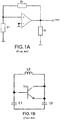
- LC-type sine wave oscillators In the systems known in the state of the art, LC-type sine wave oscillators, a generic diagram of which is shown in figure 1A , are used.
- the electronic circuit generates a medium-high frequency signal (kHz-MHz) using active components and a resonance network (coil-condenser).
- the amplifier can be implemented by a field-effect transistor, a bipolar transistor or by an operational amplifier.
- the two basic topologies deriving from the oscillator in figure 1A such as the Colpitts oscillator shown in figure 1B and the Hartley oscillator ( US1356763 , US2556296 ) shown in figure 1C .
- the quality, or Q, factors are relatively low, enabling the resonant tank circuit to oscillate over a wide range of frequencies.
- Another known typology of circuit is the Armstrong LC-type oscillator ( US11131149 , DE291604 ) shown in figure 1D .
- the design and implementation of an oscillator circuit that minimises the parasitic capacities generated by the circuit itself, and by the electrode or antenna that generates and receives the EM field, is required.
- the senor should be operative within a wireless sensor network.
- the wireless technology used should be suitable for low-consumption and low-data-transfer rate at the same time as achieving a high level of reliability and security in the communications that enable its integration with other types of sensors, such as optical sensors, CCD sensors or any other type of sensors.
- Document WO9741458 describes a quasi-electrostatic detection system that surrounds an electrically conductive mass with an electric field the magnitude of which is detected in one or more locations to analyse a property of interest with respect to the mass.
- the object intercepts a part of the electric field that extends between the "emitter” electrode coupled to a CA and the other "receiver” electrodes, the amount of the field intercepted according to the size and orientation of the mass detected, regardless of whether or not the mass provides an earth connection pathway, and the geometry of the electrodes distributed. Due to the response of the field to an object being a complex non-linear function, the addition of electrodes can always be distinguished among other cases. In other words, each electrode represents an independent weighting of the mass within the field; adding an electrode provides information with respect to that mass which is not redundant for the information provided by the other electrodes.
- Document WO03022641 describes a device for detecting the size and location of an occupant of a vehicle which includes a conductor that is electrically coupled to a voltage signal generator and fitted inside the vehicle seat. The conductor generates a periodic electric field. A plurality of electrostatic sensor antennae are fitted adjacent to the roof and are capable of detecting at least one part of the electric field. A detection circuit determines the size and location of a vehicle occupant based on an incidental quantity of electric field in each electrostatic antenna of the sensor.
- Document US2004090234 describes well-logging devices and methods for determining the resistivity of the formation to multiple (>3) research depths. At least one transmitter antenna and at least two receiver antennae which are mounted in a logging tool casing, in a substantially common axis. The antennae are untuned wire coils. The electromagnetic energy is emitted at multiple frequencies from the transmitter to the formation. The receiver's antennae, which are separated from each other and from the transmitter, detect the electromagnetic energy reflected.
- document EP256805 describes a sensor comprising an analysis and control circuit and a reference electrode coupled to the analysis and control circuit.
- the electrode sensor of a capacitive sensor is coupled to said analysis and control circuit.
- the capacitive sensor is adapted to detect the proximity of an object.
- the analysis and control circuit of the sensor is designed so that the capacitance data detected between the sensor electrode and the reference electrode are variable to the potential of an objective electrode by means of an analysis and control circuit of the sensor.
- the above documents display the particularity of being configured by means of an emitter-receiver structure, in other words, that there is an electrode that emits and an electrode that receives a particular signal, and so the disruptions between said emitter and said receiver are measured. Meanwhile, this presents a certain complexity in the circuitry. Furthermore, it does not permit the emission of the magnetic field to be controlled since the dispersion in the emitter is not defined in a determined direction so that it does not restrict its use and application to very specific cases wherein it is possible to implement or use both emitters and receivers.
- Document EP2980609 describes a sensor capable of measuring electrostatic fields and their variations to determine human presence in an area close to and surrounding said probe and differentiate it from any other animal or object.
- the electrostatic fields sensor whose signals are uncoupled from each other by means of an uncoupling circuit, and wherein said circuits for measuring electrostatic fields are connected to an antenna consisting of a coaxial cable by means of a phase measurement circuit.
- This invention shares the same technical objective and resolves the same technical problems as this document, albeit with an alternative and different solution.
- This invention is based on the measurement of the variation of a controlled magnetic field surrounding a conductor that acts like a probe or antenna when said body is affected by the influence of a charged body such as the human body.
- a charged body such as the human body.
- the human body just like any other existent body, presents intrinsic electrical characteristics, dependent on the materials, density, volume, temperature and conductivity. Potential differences between the different objects give rise to electrostatic discharges from one object to another when they come into contact or are infinitesimally close. This effect is exploited by the sensor that is the object of this invention, managing to measure continuously the fluctuations that said field cause in a circuit connected to the conductor that acts like an antenna. Notwithstanding, this invention describes a series of improvements to the technology described in the state of the art as will be described in detail in this document.
- the document US5764145A discloses a capacitive detector which includes an antenna for detecting small capacitive changes in an electric or electromagnetic field surrounding the antenna, and particularly to an alarm system which uses the capacitive detector to generate an alarm signal upon detection of capacitive changes in the generated electric or electromagnetic field.
- the detector is realized with an antenna connected to an electronic circuitry which generates an electric field around the antenna.
- the electronic circuitry generates an electric or electromagnetic field around the antenna, builds up a balanced electric field around the antenna, maintains the generated electric or electromagnetic field around the antenna balanced, prevents the detector device from being affected by changes in temperature and humidity, detects small changes in the generated electric field around the antenna, and indicates that a change in the generated electric field has occurred.
- the object of this invention is a device comprising a controlled magnetic fields sensor with which it is possible to detect the presence of any nearby object by means of the detection of the disruption in a magnetic field around a sole conductor which is configured as an antenna that emits a controlled magnetic field and, at the same time, detects the variation or disruption to said field. All this according to the device described in claim 1. In the depending claims to it, specific embodiments of the device of the invention are described. Other aspects of the invention are described in independent embodiments.
- One of the virtues of this invention is that it is capable of emitting the electromagnetic field in a controlled way by means of an active screening by means of a high impedance circuit so that, by means of the only conductive element comprising the emitter-receiver antenna, it is possible to direct the magnetic field towards a determined zone of influence and configurable for each specific application as will be described subsequently in this document.
- the device is capable of distinguishing, as a function of the magnitude of the change -i.e., the disruption generated- if there is a person, an animal or any other object, since the invention is based on the device's capacity to measure the variations of the magnetic field existent around each one of the antennae the device is connected to, since the device can be connected to various antennae, with the particularity that each one of the antennae acts independently with respect to the others, in other words, each antenna has the same capabilities and functionalities in the detection of the disruption -it emits a controlled magnetic field and, at the same time, detects disruptions to this field-.
- the device's operating principle is simple.
- the device essentially comprises an oscillator circuit that generates a sine wave (alternating current) and whose output is connected to at least one antenna like those indicated.
- the circuit has the particularity of being a closed loop since the signal from the antenna is, at the same time, configured as the input signal from the oscillator circuit.
- This particular configuration enables the antenna signal to be followed, in other words, when there is a disruption and the magnitude of the field changes, this change will immediately affect the input of the oscillator circuit, thereby significantly increasing the sensitivity of the device and, furthermore, makes the traditional emitter-receiver configuration described in the state of the art unnecessary.
- this invention just like document EP2980609 starts from the fact that, the human body, just like any other existent object, displays its own electrical characteristics, dependent on the materials, density, volume, temperature and conductivity.
- the differences of potential between different objects give rise to a plurality of electrostatic interactions from one object to another when they enter into contact or are nearby. This effect generates fluctuations in the magnetic field surrounding the antenna, which are continuously measured by the device.
- the measurement of this signal from the antenna due to a disruption - i.e., the measurement of the change in the antenna's impedance due to a disruption- in turn shapes the controlled magnetic field surrounding the antenna and enables it to be determined, according to the change caused, which object has caused said disruption -person, animal or thing-.
- the device for measuring disruptions in a controlled magnetic field and generated by the device itself surrounding a sole conductive element, antenna or electrode comprising, at least: a controlled magnetic fields device comprising, in turn: an oscillator circuit connected to at least one electrode, a digital module; and a processor connected to the digital module; wherein said measurement device is characterised because: the oscillator is connected to a transformer whose secondary is connected to the electrode and whose primary is connected to the active element of the oscillator; the oscillator comprises a feedback network and a polarisation network configured to polarise the input transistors of the active element of the oscillator; and wherein, moreover, the signal generated by the active element of the oscillator generates a controlled magnetic field in the electrode and this same signal recharges the input of the active element of the oscillator by means of the feedback network; so that the same signal that recharges the input of the active element of the oscillator is processed digitally in the digital module to be acquired by the processor.
- a controlled magnetic fields device comprising, in turn
- the applications of the device that is the object of the invention are all those requiring the detection of an object prior to it resulting in the violation of the restricted space.
- these applications we can highlight the following: the localisation of people, domestic and industrial security applications, robotics, military applications and security applications for transporting cargo and people, work-related and domestic prevention and security applications and applications for the logistics sector.
- the device applied to security systems in industrial installations involves notifying a specific user or operator that he/she is approaching a determined restricted or unauthorised zone. This enables -for example, in the operational zone of a robot arm, for it to be paralysed when an operator is within its operating range, regardless of whether the operator him/herself is subsequently called upon to explain if he/she were not authorised to be there, for which purpose the system can also identify the operator.
- object of the invention is an access control in restricted areas comprising at least one of the following: a virtual fence, a crossings detector in sensitive, restricted or dangerous zones such as railway platforms or loading docks for land or maritime transport, as well as safety in the use of domestic appliances; or a combination of the above.
- the virtual fence or crossings detector comprises, at least, a device according to this invention, with the particularity of having a plurality of antennae configured to delimit a determined work or transit area, so that any object, person or animal that affects, at least, one generated field in, at least, one of the antennae, generates an alarm, a notification or similar. It is also intended that said signal might activate some kind of physical closure element -for example, the automatic closing of a door or physical barrier-.
- the device of this invention can be used in the surveillance and control of railway platforms, loading docks for land or maritime transport, access to safes, monitoring exhibitions of valuable objects, such as works of art, and safety control in the use of domestic appliances.
- the antenna or antennae delimit a determined control area or restricted use zone, so that any object, person or animal that generates a disruption in at least one antenna connected to at least one device will generate an alarm, a notification, or similar. It is also intended that said signal might activate some kind of physical closure element -for example, the automatic closing of a door or physical barrier-.
- an object of this invention is a detector of objects adhered to a vehicle by means of the detection of the approach of the person and/or the characterisation of the foreign element.
- it is configured as a security element inside vehicles, for example, in the detection of the correct position of security anchors or the detection of people in bathrooms, cellars or restricted areas of the vehicles themselves, such as the driver's cab.
- the security system is capable of precisely detecting the position of the vehicle in a car park or parking area.
- Another object of the invention is its use as a weapons and explosives detector and a method for the detection of weapons and explosives. More specifically, this invention refers to the detection of IEDs ( Improvised Explosive Devices ) in the passage of vehicles, the detection of limpet bombs, the detection of land mines or the detection of weapons, by means of the detection of the approach of the person or characterisation of a foreign element that may, in itself, be deemed a threat.
- IEDs Improvised Explosive Devices
- the device of the invention is used for the detection of the intrusion before it takes place, precisely thanks to its capacity to measure the disruptions at distance.
- the different aspects of the invention comprise a controlled magnetic field sensor capable of detecting a disruption in the magnetic field surrounding a sole conductor or antenna that has the particularity of emitting a controlled magnetic field and, at the same time, detecting any disruption in said field so that, by means of the characterisation of said disruption, it is possible to detect and discern the object that generated said disruption.
- circuit and «circuitry» refer to the electronic physical components -i.e., hardware components- and any software and/or firmware -machine code- that can configure or be susceptible to configuring the hardware and/or be associated in any way with the hardware.
- hardware and software may be abbreviated to HW and SW respectively.
- a sensor CMF 100 is shown, which is a mixed analogue-digital sensor comprising an oscillator 102 connected to, at least, one antenna 101 embodied in a sole conductive element which is configured to emit an electromagnetic field and which, in turn, is an EM field emitter and a receiver of said EM field, being capable of receiving and detecting the disruptions generated in said field due to the presence of one that is converted into a square wave and digitalised for its subsequent analysis as will be described below.
- the expressions «antenna», «conductor» and «electrode» refer to the same physical element, i.e., an electrical conductor referenced as (101) and whose equivalent circuit is a capacity condenser that is variable as a function of the presence of an object, person or animal that disrupts the controlled magnetic field generated by the oscillator 102 surrounding the antenna or electrode 101.
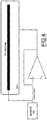
- the controlled magnetic field is directable by means of an active gatekeeper, as shown in figure 4 .
- a high impedance element is implemented-in the embodiment shown in figure 4 , an operational amplifier-.
- the sensor 100 and the electrode 101 are connected to the input of the device.
- the output of the device is earthed, so there is a very high impedance at the input (of the order of 100 M ⁇ ) and a low impedance at the output (of the order of 5/10P ⁇ ), which causes the lines of the field to be emitted in just one direction.
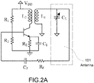
- the oscillator 102 is configured to minimise the parasitic capacities generated by the circuit itself and by the electrode 101 and which guarantees a continuous oscillation of the sine wave. Notwithstanding, when the design of the oscillator 102 has to be implemented within a chip and in CMOS technology, the parasitic effects of the transformer (L1, L2) as well as the parasitic capacities and parasitic resistances themselves of an integrated design were evaluated, taking into account that the transformer (L1, L2) is directly connected to a pad of the chip, as shown better in figure 2B .
- the two-stage topology is the one that delivers highest gains but also needs a higher compensation and its power consumption is higher. Although adequate, its high-power consumption rules it out for this application since each sensor 100 node must have a high autonomy of use.
- the telescopic configuration has been chosen as a preferred, but non-limiting, embodiment because it consumes less power, achieves higher gains and has parasitic poles at very high frequencies.
- the sine wave voltage at this point is between 2 - 200 volts peak-to-peak (Vpp).
- the feedback of this point is connected to the MOS (M IN ) transistor gate of the active element (i.e. the operational amplifier in telescopic configuration) and the maximum voltage that an MOS transistor can withstand is around 7V, for which the circuit shown in figure 2B is used, as previously indicated.
- the feedback network (R F , C F ) of the oscillator 102 circuit has been modified to manage the signals from tens of volts generated in the electrode 101 within the integrated circuit -the chip.
- the R BIAS resistance and the V BIAS polarisation voltage have been included.
- the R BIAS resistance, along with the R F resistance, form a voltage divider that mitigates the oscillation at the input to the active element and which, moreover, along with the V BIAS voltage, ensures that negative voltages, which may endanger the integration of the circuit, are not reached.
- the fact that the integrated circuit is designed in CMOS technology enables the R BIAS resistance and the V BIAS voltage also to be used to adequately polarise the (M IN ) input transistor of the active element of the oscillator 102.
- the mitigated sine wave signal at the input of said active element can be converted into a low voltage feedback environment within the integrated circuit itself in a squared signal for its subsequent digital processing.
- the polarisation voltage of the (V BIAS ) oscillator should be 5V -but in a non-limiting way, since other values can be adopted according to the technology implemented for the physical embodiment of the device- so that around 5V of maximum sine wave voltage reaches the gate of the (M IN ) input transistor of the operational amplifier, so that, along with the appropriate relationship of transformer coils, the required voltage of 2-200 Vpp is generated in the secondary (L2).
- the polarisation resistance (R BIAS ) in the input of the telescopic amplifier is also included within the integrated circuit.
- the gain of the amplifier is reduced and the oscillation condition may be lost and it has been proved that, with load capacities in the electrode 101 of between 1 pF and 10nF, oscillation frequencies between 5 kHz and 2MHz are generated with amplitudes of between 2-200Vpp, detecting capacity variations of 0.01 pF, which supposes a frequency change detectable by the circuit.
- these numerical examples have a purely illustrative and non-limiting value in the operation and benefits of this invention.
- the digital part of the sensor or digital module 103 is described. That is to say, once the analogue part provides sufficient amplitude voltage to the electrode 101 to generate the EM field (2-200Vpp) and the inverters have generated a squared signal typically of between 0-5 V-this value, likewise non-limiting, will depend on the final technology used in the physical embodiment of the device- the latter being the signal that should be processed in the digital domain to extract the information of interest.
- the circuit in the digital domain 103 is configured to connect to the processor 105 by means of an SPI port ( Serial Port Interface, described in technical note TN0897 Technical Note ST SPI Protocol ) in slave mode.
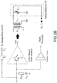
- Figure 3 shows the block diagram of the digital circuit 103 of the sensor CMF 100.
- the device of the invention is configured in a particular embodiment, as a matrix of sensors 100 with 8 channels (i.e. eight sensors 100 each connected to at least one electrode 101).
- This configuration enables the device to undertake the measurement of the controlled magnetic field in differential format, each sensor 100 acts in parallel, so that one of the channels can be used as a gatekeeper against noise.
- the matrices -the sensors 100 configured in the form of a matrix within the ASIC integrated circuit- have cross-talking problems due to their physical proximity.
- the device of the invention implements an internal and external synchronisation mechanism of the measurement of the sensors 100 whereby:
- FIG. 3 Another important benefit of the device of the invention, shown in figure 3 , is that it is possible to not work continuously, but by storing everything in a buffer so that energy can be saved because all the data remain stored in the buffer can be analysed a posteriori, and not necessarily continuously. Furthermore, as we shall see below, all the parameters are programmable.
- the sensor 100 comprises, in turn, the following input-output blocks or modules:
- the SAMP signal is an input used as an initial sampling signal.
- This signal uses an internal register with a time period configured not to overlap the measurements of the different devices and to not cause interferences.
- the sensor CMF 100 is internally configured to establish the sampling frequency and to determine whether the transitional has passed, two registers are activated:
- the sensor CMF 100 is configured to record, on the one hand, the last measurement, indicating its electrode 101 of origin and, on the other hand, comprises up to 64 registers with the last measurements wherein the registers can always be accessed in the same direction, like a circular stack. In light of successive readings, the system will return the samples, starting with the most recent until the queue is cleared. For each measurement, the measurement electrode is identified.
- the sensor CMF 100 is connected wirelessly to a management system 1 that is configured as a computer or central processing unit that can either be integrated into one sole device or be a distributed system.
- An integrated system may comprise, for example, a sole computer or central processing unit (CPU), server, electronic machine or device, in which the integrated system can be configured to perform some or all of the functions or characteristics of management system 1, as described in this document.
- a distributed system can be implemented with a plurality of interconnected components, preferably wirelessly, and wherein each component is configured to carry out all or some of the functions, characteristics and/or operation of management system 1.
- management system 1 implements one or more nodes, embodied in one or more master-type controllers to control one or more sensors CMF 100.
- a master controller may also comprise, for example, a remote controller.
- FIG3 refers to a unique management system 1, logically, the description is not limited to just one embodiment.
- Communications between the sensor CMF 100 and the management system 1 are essentially wireless and may comprise different links and/or protocols such as, for example, Bluetooth, ZigBee, Bluetooth LE, Smart Bluetooth, iBeacon, near-field communication (NFC) protocols or WLAN WIFI (protocols 802.11) or any other wireless link or suitable protocols for the interchange of data between the management system 1 and the sensor or sensors CMF 100.
- protocols such as, for example, Bluetooth, ZigBee, Bluetooth LE, Smart Bluetooth, iBeacon, near-field communication (NFC) protocols or WLAN WIFI (protocols 802.11) or any other wireless link or suitable protocols for the interchange of data between the management system 1 and the sensor or sensors CMF 100.
- NFC near-field communication
- WLAN WIFI wireless link or suitable protocols for the interchange of data between the management system 1 and the sensor or sensors CMF 100.
- the management system 1 can also communicate with at least one user terminal 4 by means of the data network 3. Communication can be direct or by means of an external service server, for example, in certain cases or applications, an alarm centre, the result being in any case the same, which is no different from communicating the incidences measured by the sensor CMF 100 to the owner of user terminal 4.
- This user terminal is a mobile phone, tablet or personal computer and, in general, any electronic device capable of receiving and interpreting the data originating from management system 1 by means of data network 3, or a mobile phone network or a combination of both.
- the sensor CMF 100 can define its own position by means of, for example, GPS, IPS and/or micro-mapping and/or based on a reference position defined in management system 1. For example, if the sensor CMF 100 moves from the desired position, a notification will be sent to the management system and, thus, to user terminal 4 by means of data network 3. Similarly, the detection of any disruption to the magnetic field surrounding at least one sensor CMF 100 may generate an order from management system 1 or from user terminal 4 in order to generate a required action according to each case and specific application, as will be explained for each specific use of this invention.
- the sensor CMF 100 comprises a programme or programmes that are stored in the memory 106 and configured to be executed by one or more processors 105.
- the programmes comprise instructions to execute the functionalities previously described.
- the memory 106 can store, for example, configuration data that may comprise parameters and/or code comprising software and/or firmware.
- the memory 106 may comprise different memory technologies, including, for example, read-only memory (ROM), programmable ROM and electronically-erasable EEPROM, random-access memory (RAM), low-latency non-volatile memory, flash memory, solid-state drive (SSD), field-programmable gate array (FPGA) and/or other means of electronic data storage capable of storing data, code and/or other information.
- the memory 106 can be used to store the processed data generated by the electrode 101.
- the memory 106 can also be used for storing information, such as configuration information, that can be used for controlling the operation of the sensor CMF 100.
- the memory 106 may comprise information required to configure the wireless transceiver to enable the reception of RF signals in the appropriate frequency band and the desired communications protocol.
- the sensor CMF 100 may be operable to receive software and/or firmware updates which could be stored in a memory (for example, the memory 106).
- the sensor CMF 100 can receive software and/or firmware updates from a network manager (for example, management system 1).
- a network manager for example, management system 1.
- the process can be completely automatic (for example, a network administrator may send an update to the sensor CMF 100), and/or semi-automatic (for example, an update may be initiated by a user by means of, for example, user terminal 4).
- the battery 107 may comprise a replaceable battery inside the sensor CMF 100to provide energy, or as back-up power when DC input voltage is used.
- the sensor CMF 100 can take measurements of the sensors and/or communicate with other lower frequency devices when powered by the battery 107 and can only detect/communicate continuously when an external DC power source is used, thus achieving energy savings.
- the wireless long-range sensor 108 may comprise the logic or appropriate circuits to for example, determine whether the sensor CMF 100 is within range of a management system 1. To this effect, the wireless long-range sensor may be operable to generate an alarm condition when the sensor CMF 100 is not within range of management system 3. In an example embodiment, if the sensor CMF 100 is out of range, it can generate a luminous signal in the luminous indicators or an acoustic signal in an acoustic indicator.
- the sensor CMF 100 comprises a wireless transceiver 109, which may comprise the appropriate circuits and logic for the communication by means of one or more wireless communications protocols, such as Z-Wave, IEEE 802.11x, Bluetooth, and ZigBee.
- the wireless transceiver 109 may therefore comprise RF transmission media, the amplification, the demodulation/modulation and other circuits for the transmission and reception of signals.
- the wireless transceiver 109 can be used to provide software/firmware updates for the sensor CMF 100.
- the sensor CMF 100 comprises a programme or programmes stored in the memory 106 and configured to be executed by means of one or more processors 105.
- the programmes comprise instructions to execute the functionality of the device described.
- various means of embodiment provided by this description may be implemented using hardware, software, or combinations of hardware and software.
- the different components of hardware and/or software established in this document may be combined in composite materials comprising software, hardware and/or both, without deviating from the object of this invention defined by its claims.
- the different components of hardware and/or software established in this document can be separated in the sub-components comprising software, hardware, or both, without deviating from the object of this invention defined by its claims.
- the software components can be used as hardware components and vice versa.
- the software according to this description can be stored in one or more legible means of the non-transitory machine. It is also considered that the software identified in this document can be implemented using one or more general-purpose, or specific-purpose, computers and/or computer systems, in a network and/or of another type. As the case may be, the order of the different steps described in this document can be changed and/or divided into substages to deliver the characteristics described in this document.
Landscapes
- Physics & Mathematics (AREA)
- General Physics & Mathematics (AREA)
- Electromagnetism (AREA)
- Engineering & Computer Science (AREA)
- Remote Sensing (AREA)
- Life Sciences & Earth Sciences (AREA)
- Condensed Matter Physics & Semiconductors (AREA)
- Geology (AREA)
- Environmental & Geological Engineering (AREA)
- General Life Sciences & Earth Sciences (AREA)
- Geophysics (AREA)
- Geophysics And Detection Of Objects (AREA)
- Arrangements For Transmission Of Measured Signals (AREA)
- Emergency Alarm Devices (AREA)
- Magnetic Ceramics (AREA)
- Measuring Magnetic Variables (AREA)
- Magnetic Resonance Imaging Apparatus (AREA)
- Burglar Alarm Systems (AREA)
Claims (17)
- Ein Messgerät zum Messen von Störungen in einem gesteuerten Magnetfeld, umfassend:mindestens eine Elektrode (101), die aus einem einzigen leitenden Element besteht, das von dem von der Vorrichtung erzeugten gesteuerten Magnetfeld umgeben ist;einen gesteuerten Magnetfeldsensor (100), der in einem geschlossenen Regelkreis mit der mindestens einen Elektrode (101) verbunden ist, wobei der Sensor umfasst:einen Oszillator (102), der ein aktives Element umfasst, wobei der Oszillator mit der mindestens einen Elektrode (101) gekoppelt ist,ein digitales Modul (103); undeinen Prozessor (105), der mit dem digitalen Modul (103) verbunden ist;wobei der Oszillator (102) mit einem Transformator (L1, L2) verbunden ist, dessen Sekundärwicklung (L1) mit der mindestens einen Elektrode (101) verbunden ist und dessen Primärwicklung (L2) mit dem aktiven Element des Oszillators (L2) verbunden ist 102); undder Oszillator (102) umfasst ferner ein Polarisationsnetzwerk (RBIAS, VBIAS), das konfiguriert ist, um mindestens einen Eingangstransistor (MIN) des aktiven Elements des Oszillators (102) zu polarisieren;wobei ferner das vom aktiven Element des Oszillators (102) erzeugte Signal ein gesteuertes Magnetfeld in der mindestens einen Elektrode (101) erzeugt und dasselbe Signal dem Eingang (MIN) des aktiven Elements des Oszillators zugeführt wird (102) über ein Rückkopplungsnetzwerk (RF, CF); so dass das gleiche Signal, das an den Eingang (MIN) des aktiven Elements des Oszillators (102) angelegt wird, in dem vom Prozessor (105) zu erfassenden digitalen Modul (103) digital verarbeitet wird.
- Messvorrichtung nach Anspruch 1, wobei das aktive Element eine Topologie aufweist, die ausgewählt ist zwischen: Teleskop, gefalteter Kaskode und zweistufig.
- Messvorrichtung nach Anspruch 1, wobei das Signal, das den Eingang (MIN) des aktiven Elements des Oszillators (102) auflädt, digital verarbeitet wird, indem ein Sinuswellensignal mittels einer Adapterschaltung auf ein Quadratsignal übertragen wird.
- Messvorrichtung nach einem der Ansprüche 1 bis 3, die als integrierte Schaltung konfiguriert ist, die eine Matrix von gesteuerten Magnetfeldsensoren (100) integriert und einen Synchronisationsmechanismus der Messung der Sensoren (100) der Matrix implementiert wobei: (a) die Sensoren (100), die sich in nächster physikalischer Nähe befinden, Messzyklen oder Zeiträume aufweisen, die zeitlich getrennter sind; und (b) die Sensoren (100), die physikalisch weiter entfernt sind, haben engere Messzeiträume zwischen sich.
- Vorrichtung nach Anspruch 4, wobei das digitale Modul (103) ein Signal umfasst, das konfiguriert ist, um als ein anfängliches Abtastsignal (SAMP) verwendet zu werden, wobei dieses Signal ein internes Register mit einer Zeitperiode verwendet, die so konfiguriert ist, dass es die Messungen nicht überlappt der verschiedenen Sensoren und verursacht keine Störungen.
- Messvorrichtung nach einem der Ansprüche 1 bis 5, wobei das digitale Modul (103) wiederum einen Messpuffer umfasst, in dem alle von mindestens einem Sensor (100) während eines programmierbaren Zeitraums durchgeführten Messungen gespeichert sind.
- Messvorrichtung nach Anspruch 6, wobei der Sensor (100) konfiguriert ist, um einerseits die letzte Messung aufzuzeichnen, die seine Ursprungselektrode (101) anzeigt, und andererseits bis zu 64 Register mit der Letzte Messungen, bei denen auf die Register immer in derselben Richtung zugegriffen werden kann, so dass angesichts aufeinanderfolgender Ablesungen die Messungen zurückgegeben werden, beginnend mit der letzten bis zum Löschen der Warteschlange.
- Messvorrichtung nach einem der vorhergehenden Ansprüche, wobei das digitale Modul (103) umfasst:a) ein Kommunikationsmodul in Reihe mit dem Prozessor (105), einschließlich:ein Takteingangssignal (SCK)ein serielles Datenausgangssignal (SDO) an den Prozessor (105)ein serielles Dateneingangssignal (SDI) vom Prozessor (105) zum sensorgesteuerten Magnetfeldsensor (100);ein Auswahlsignal für einen gesteuerten Magnetfeldsensor (100);b) ein Modul von Unterbrechungssignalen, umfassend:ein erstes Unterbrechungssignal (INT_MES), das anzeigt, dass gerade eine Messung durchgeführt wurde und das konfigurierbar ist, um eine Vielzahl von gesteuerten Magnetfeldsensoren (100) in Reihe zu schalten;ein zweites Unterbrechungssignal (INT_LAST), das anzeigt, dass die Differenz zwischen der aktuellen und der letzten Messung einen konfigurierten Schwellenwert überschritten hat;ein drittes Unterbrechungssignal, das anzeigt, dass die Differenz zwischen dem Strom und dem Durchschnitt der letzten Messungen den Schwellenwert überschritten hat, wobei die Anzahl der Messungen zur Berechnung des Durchschnitts konfigurierbar ist;c) ein Elektrodenauswahlmodul, das als Ausgangssignal mit 8 codierten Bits konfiguriert ist und den Schalter aktiviert, der die Messelektrode (101) auswählt, wobei jeder Sensor (100) mit einer der Elektroden (101) verbunden werden kann, die dies wäre konfiguriert als Emitter-Empfänger-Antenne des gesteuerten Magnetfeldes.
- Vorrichtung nach einem der Ansprüche 1 bis 8, wobei der Sensor (100) intern konfiguriert ist, um die Abtastfrequenz festzulegen und festzustellen, ob der Übergang bestanden hat, wodurch zwei Register aktiviert werden:a) Wenn sich die vorherige und die letzte Stichprobe um einen niedrigeren Wert als einen Epsilon-Wert unterscheiden, wird davon ausgegangen, dass der Übergang bestanden hat und die Messung beginnt. und / oderb) Angeben der Einrichtungszeit, um zu bestimmen, ob das Signal der Elektrode (101) stabil ist.
- Verwendung der Vorrichtung nach einem der Ansprüche 1 bis 9 bei der Lokalisierung von Personen, wobei die Verwendung das Messen von Störungen in einem kontrollierten Magnetfeld umfasst.
- Verwendung der Vorrichtung nach einem der Ansprüche 1 bis 9 in Sicherheitssystemen in Industrieanlagen, wobei die Verwendung eine Warnung an einen bestimmten Benutzer oder Mitarbeiter beinhaltet, dass er sich einer bestimmten eingeschränkten oder nicht autorisierten Zone nähert, die durch mindestens eine Antenne begrenzt ist (101), die eine Einflusszone des kontrollierten Magnetfelds konfiguriert und mindestens eines der folgenden Elemente umfasst: einen virtuellen Zaun, einen Kreuzungsdetektor in empfindlichen, eingeschränkten oder gefährlichen Zonen wie Eisenbahnplattformen oder Ladedocks für den Land- oder Seeverkehr sowie Sicherheit bei der Verwendung von Haushaltsgeräten; oder eine Kombination der oben genannten.
- Verwendung der Vorrichtung nach einem der Ansprüche 1 bis 9 in industriellen Robotermaschinen und Haushaltswerkzeugen, wobei die Verwendung das Messen von Störungen in einem gesteuerten Magnetfeld umfasst.
- Verwendung der Vorrichtung nach einem der Ansprüche 1 bis 9 in Fahrzeugen, umfassend: (a) die Erfassung von an einem Fahrzeug haftenden Gegenständen mittels der Erfassung der Annäherung der Person und / oder der Charakterisierung des Fremdelements; oder (b) in der inneren Sicherheit von Fahrzeugen durch Erkennen der Position mindestens eines Benutzers; (c) bei der Erfassung der Position eines Fahrzeugs auf einem Parkplatz oder Parkplatz; oder (d) Sicherheit beim Transport von Fracht oder Personen.
- Verwendung der Vorrichtung nach einem der Ansprüche 1 bis 9 zur Aufdeckung von Waffen und Sprengstoffen, umfassend: Aufdeckung von improvisierten Sprengvorrichtungen beim Durchgang von Fahrzeugen, Aufdeckung von Napfschneckenbomben, Aufdeckung von Landminen oder Aufdeckung von Waffen durch Mittel zur Erfassung der Annäherung der Person oder zur Charakterisierung eines Fremdelements, das an sich als Bedrohung angesehen werden kann, wobei die Verwendung das Messen von Störungen in einem kontrollierten Magnetfeld umfasst.
- Verwendung der Vorrichtung nach einem der Ansprüche 1 bis 9 in Haussicherheitsanwendungen zur vorbeugenden Erkennung von Eindringlingen an Türen, Fenstern, Wänden oder allgemein einem anderen architektonischen Verschluss, wobei die Vorrichtung zur Erkennung des Eindringens verwendet wird bevor es stattfindet, durch Messen von Störungen in einem kontrollierten Magnetfeld in der Ferne.
- Verwendung der Vorrichtung nach einem der Ansprüche 1 bis 9 in arbeitsbezogenen oder häuslichen Präventions- und Sicherheitsanwendungen, wobei die Verwendung das Messen von Störungen in einem kontrollierten Magnetfeld umfasst.
- Verwendung der Vorrichtung nach einem der Ansprüche 1 bis 9 in Logistikanwendungen, einschließlich der Steuerung des Frachttransports, wobei die Verwendung das Messen von Störungen in einem kontrollierten Magnetfeld umfasst.
Priority Applications (17)
| Application Number | Priority Date | Filing Date | Title |
|---|---|---|---|
| EP18382251.9A EP3553477B1 (de) | 2018-04-13 | 2018-04-13 | Gerät zur messung einer störung in einem kontrollierten magnetfeld |
| PT183822519T PT3553477T (pt) | 2018-04-13 | 2018-04-13 | Aparelho de medição de perturbações num campo magnético controlado |
| DK18382251.9T DK3553477T3 (da) | 2018-04-13 | 2018-04-13 | Anordning til måling af forstyrrelse i et kontrolleret magnetfelt |
| PL18382251T PL3553477T4 (pl) | 2018-04-13 | 2018-04-13 | Urządzenie do pomiaru zakłóceń w kontrolowanym polu magnetycznym |
| ES18382251T ES2848174T3 (es) | 2018-04-13 | 2018-04-13 | Aparato de medida de las perturbaciones en un campo magnético controlado |
| AU2019250691A AU2019250691A1 (en) | 2018-04-13 | 2019-04-13 | Device to measure disruptions in a controlled magnetic field |
| BR112020020928-7A BR112020020928A2 (pt) | 2018-04-13 | 2019-04-13 | dispositivo para medição de interrupções em um campo magnético controlado |
| MX2020010788A MX2020010788A (es) | 2018-04-13 | 2019-04-13 | Aparato de medida de las perturbaciones en un campo magnetico controlado. |
| CA3096966A CA3096966A1 (en) | 2018-04-13 | 2019-04-13 | Device to measure disruptions in a controlled magnetic field |
| EP19716912.1A EP3797270B1 (de) | 2018-04-13 | 2019-04-13 | Verfahren zur messung von störungen in einem kontrollierten magnetfeld |
| ES19716912T ES2980570T3 (es) | 2018-04-13 | 2019-04-13 | Método de medición de perturbaciones en un campo magnético controlado |
| CN201980029150.6A CN112041641B (zh) | 2018-04-13 | 2019-04-13 | 用以测量受控磁场的间断的设备及其用途 |
| US17/046,966 US11867863B2 (en) | 2018-04-13 | 2019-04-13 | Device to measure disruptions in a controlled magnetic field |
| JP2021504579A JP7356495B2 (ja) | 2018-04-13 | 2019-04-13 | 制御された磁場の乱れを測定するためのデバイス |
| KR1020207031547A KR20200143696A (ko) | 2018-04-13 | 2019-04-13 | 제어된 자기장에서 교란을 측정하는 장치 |
| PCT/EP2019/059585 WO2019197677A1 (en) | 2018-04-13 | 2019-04-13 | Device to measure disruptions in a controlled magnetic field |
| IL278027A IL278027B2 (en) | 2018-04-13 | 2020-10-13 | A device for measuring disturbances in a controlled magnetic field |
Applications Claiming Priority (1)
| Application Number | Priority Date | Filing Date | Title |
|---|---|---|---|
| EP18382251.9A EP3553477B1 (de) | 2018-04-13 | 2018-04-13 | Gerät zur messung einer störung in einem kontrollierten magnetfeld |
Publications (2)
| Publication Number | Publication Date |
|---|---|
| EP3553477A1 EP3553477A1 (de) | 2019-10-16 |
| EP3553477B1 true EP3553477B1 (de) | 2020-10-14 |
Family
ID=62116363
Family Applications (2)
| Application Number | Title | Priority Date | Filing Date |
|---|---|---|---|
| EP18382251.9A Active EP3553477B1 (de) | 2018-04-13 | 2018-04-13 | Gerät zur messung einer störung in einem kontrollierten magnetfeld |
| EP19716912.1A Active EP3797270B1 (de) | 2018-04-13 | 2019-04-13 | Verfahren zur messung von störungen in einem kontrollierten magnetfeld |
Family Applications After (1)
| Application Number | Title | Priority Date | Filing Date |
|---|---|---|---|
| EP19716912.1A Active EP3797270B1 (de) | 2018-04-13 | 2019-04-13 | Verfahren zur messung von störungen in einem kontrollierten magnetfeld |
Country Status (15)
| Country | Link |
|---|---|
| US (1) | US11867863B2 (de) |
| EP (2) | EP3553477B1 (de) |
| JP (1) | JP7356495B2 (de) |
| KR (1) | KR20200143696A (de) |
| CN (1) | CN112041641B (de) |
| AU (1) | AU2019250691A1 (de) |
| BR (1) | BR112020020928A2 (de) |
| CA (1) | CA3096966A1 (de) |
| DK (1) | DK3553477T3 (de) |
| ES (2) | ES2848174T3 (de) |
| IL (1) | IL278027B2 (de) |
| MX (1) | MX2020010788A (de) |
| PL (1) | PL3553477T4 (de) |
| PT (1) | PT3553477T (de) |
| WO (1) | WO2019197677A1 (de) |
Cited By (1)
| Publication number | Priority date | Publication date | Assignee | Title |
|---|---|---|---|---|
| EP3797270B1 (de) * | 2018-04-13 | 2024-04-10 | Ontech Security, S.L. | Verfahren zur messung von störungen in einem kontrollierten magnetfeld |
Families Citing this family (5)
| Publication number | Priority date | Publication date | Assignee | Title |
|---|---|---|---|---|
| WO2021234185A1 (es) | 2020-05-20 | 2021-11-25 | Ontech Security, Sl | Sistema y método de gestión, control y mantenimiento predictivo en instalaciones en locales húmedos y redes de distribución de fluidos |
| WO2021245295A1 (es) | 2020-06-01 | 2021-12-09 | Ontech Security, S.L. | Dispositivo y método de pulsación sin contacto mediante detección gestual |
| EP4212890A1 (de) | 2022-01-17 | 2023-07-19 | Ontech Security, SL | Verfahren und vorrichtung zur messung von störungen in einem kontrollierten elektromagnetischen feld |
| EP4213121A1 (de) | 2022-01-17 | 2023-07-19 | Ontech Security, SL | Verfahren und vorrichtung zur messung von störungen in einem kontrollierten elektromagnetischen feld |
| KR20240159398A (ko) * | 2023-04-28 | 2024-11-05 | (주)아이티시 | 전자기파 치료 장치 |
Family Cites Families (31)
| Publication number | Priority date | Publication date | Assignee | Title |
|---|---|---|---|---|
| DE291604C (de) | 1913-04-10 | 1919-06-23 | Gesellschaft Für Drahtlose Telegraphie Mbh | Einrichtung zur erzeugung elektrischer schwingungen |
| US1113149A (en) | 1913-10-29 | 1914-10-06 | Edwin H Armstrong | Wireless receiving system. |
| US1356763A (en) | 1915-06-01 | 1920-10-26 | Western Electric Co | Oscillation-generator |
| US2556296A (en) | 1949-04-26 | 1951-06-12 | Bell Telephone Labor Inc | High-frequency transistor oscillator |
| GB1404838A (en) | 1972-08-02 | 1975-09-03 | Matsuda S | Alarm apparatus utilizing high frequency |
| FR2274174A1 (fr) * | 1974-06-05 | 1976-01-02 | Phylec | Interrupteur statique par detection de variation de capacite |
| GB8619450D0 (en) | 1986-08-08 | 1986-09-17 | Glaxo Group Ltd | Chemical compositions |
| FR2610650B1 (fr) | 1987-02-11 | 1989-10-27 | Allibert Sa | Ecran antieblouissant |
| FR2679043B1 (fr) * | 1991-07-08 | 1993-11-26 | Bertin Et Cie | Detecteur de proximite. |
| US5353011A (en) * | 1993-01-04 | 1994-10-04 | Checkpoint Systems, Inc. | Electronic article security system with digital signal processing and increased detection range |
| SE9303582D0 (sv) * | 1993-10-29 | 1993-10-29 | Goeran Hansson | Berörings- och stöldskydd för kontorsutrustning |
| JPH07131321A (ja) * | 1993-11-02 | 1995-05-19 | Keyence Corp | 磁気近接センサ |
| US5844415A (en) | 1994-02-03 | 1998-12-01 | Massachusetts Institute Of Technology | Method for three-dimensional positions, orientation and mass distribution |
| US6661115B2 (en) | 2001-09-12 | 2003-12-09 | Motorola, Inc. | Conductive e-field occupant sensing |
| US6777940B2 (en) | 2002-11-08 | 2004-08-17 | Ultima Labs, Inc. | Apparatus and method for resistivity well logging |
| US6937951B2 (en) * | 2003-06-03 | 2005-08-30 | Siemens Medical Solutions Usa, Inc. | Adaptive proximity sensing |
| JP4137893B2 (ja) * | 2005-01-31 | 2008-08-20 | アンリツ産機システム株式会社 | 金属検出装置 |
| JP4432897B2 (ja) * | 2005-12-20 | 2010-03-17 | ニッカ電測株式会社 | 金属異物検出装置 |
| CN201322805Y (zh) * | 2008-11-13 | 2009-10-07 | 刘加友 | 全数字智能型汽车防撞雷达 |
| GB201118970D0 (en) * | 2011-11-02 | 2011-12-14 | Univ Sussex | Target position,movement and tracking system |
| US9240827B2 (en) * | 2013-02-12 | 2016-01-19 | Qualcomm Incorporated | Methods and apparatus for improving remote NFC device detection using an oscillator circuit |
| ES2534702B1 (es) | 2013-09-24 | 2016-02-09 | Ontech Security, Sl | Sensor de campos electrostáticos y sistema de seguridad en espacios interiores |
| ES2565548B1 (es) * | 2014-09-03 | 2017-01-25 | Ontech Security, Sl | Sensor de campos electrostáticos y sistema de seguridad en ambientes industriales |
| JP6591755B2 (ja) * | 2015-01-22 | 2019-10-16 | 公益財団法人電磁材料研究所 | 金属検出機 |
| ES2714688T3 (es) * | 2015-04-01 | 2019-05-29 | Ontech Security S L | Sistema de seguridad doméstico |
| CN104965198B (zh) * | 2015-06-30 | 2018-04-03 | 南京理工大学 | 雷达回波模拟器频率校准的装置及方法 |
| CA3001611A1 (en) | 2015-10-19 | 2017-04-27 | Arch Wood Protection, Inc. | Biocide concentrate composition for the addition to oil-based formulations, and compositions containing the same |
| ES2615202B1 (es) | 2015-11-05 | 2018-03-15 | Ontech Security Sl | Detector de armas y explosivos y método de detección |
| FR3049068B1 (fr) * | 2016-03-16 | 2018-04-06 | Senstronic | Dispositif detecteur inductif de facteur 1 |
| EP3553477B1 (de) * | 2018-04-13 | 2020-10-14 | Ontech Security, S.L. | Gerät zur messung einer störung in einem kontrollierten magnetfeld |
| DE102018126648A1 (de) * | 2018-10-25 | 2020-04-30 | Pepperl + Fuchs Gmbh | Dynamischer Sensor für Messgeräte |
-
2018
- 2018-04-13 EP EP18382251.9A patent/EP3553477B1/de active Active
- 2018-04-13 PT PT183822519T patent/PT3553477T/pt unknown
- 2018-04-13 DK DK18382251.9T patent/DK3553477T3/da active
- 2018-04-13 ES ES18382251T patent/ES2848174T3/es active Active
- 2018-04-13 PL PL18382251T patent/PL3553477T4/pl unknown
-
2019
- 2019-04-13 MX MX2020010788A patent/MX2020010788A/es unknown
- 2019-04-13 CA CA3096966A patent/CA3096966A1/en active Pending
- 2019-04-13 WO PCT/EP2019/059585 patent/WO2019197677A1/en not_active Ceased
- 2019-04-13 AU AU2019250691A patent/AU2019250691A1/en not_active Abandoned
- 2019-04-13 JP JP2021504579A patent/JP7356495B2/ja active Active
- 2019-04-13 US US17/046,966 patent/US11867863B2/en active Active
- 2019-04-13 KR KR1020207031547A patent/KR20200143696A/ko not_active Ceased
- 2019-04-13 ES ES19716912T patent/ES2980570T3/es active Active
- 2019-04-13 CN CN201980029150.6A patent/CN112041641B/zh not_active Expired - Fee Related
- 2019-04-13 EP EP19716912.1A patent/EP3797270B1/de active Active
- 2019-04-13 BR BR112020020928-7A patent/BR112020020928A2/pt not_active Application Discontinuation
-
2020
- 2020-10-13 IL IL278027A patent/IL278027B2/en unknown
Non-Patent Citations (1)
| Title |
|---|
| None * |
Cited By (1)
| Publication number | Priority date | Publication date | Assignee | Title |
|---|---|---|---|---|
| EP3797270B1 (de) * | 2018-04-13 | 2024-04-10 | Ontech Security, S.L. | Verfahren zur messung von störungen in einem kontrollierten magnetfeld |
Also Published As
| Publication number | Publication date |
|---|---|
| AU2019250691A1 (en) | 2020-11-12 |
| US11867863B2 (en) | 2024-01-09 |
| JP7356495B2 (ja) | 2023-10-04 |
| EP3797270B1 (de) | 2024-04-10 |
| ES2848174T3 (es) | 2021-08-05 |
| EP3797270A1 (de) | 2021-03-31 |
| PT3553477T (pt) | 2021-01-20 |
| EP3553477A1 (de) | 2019-10-16 |
| IL278027B1 (en) | 2023-03-01 |
| MX2020010788A (es) | 2021-01-08 |
| CN112041641B (zh) | 2024-03-19 |
| CA3096966A1 (en) | 2019-10-17 |
| IL278027B2 (en) | 2023-07-01 |
| PL3553477T3 (pl) | 2021-05-17 |
| KR20200143696A (ko) | 2020-12-24 |
| IL278027A (en) | 2020-11-30 |
| ES2980570T3 (es) | 2024-10-02 |
| US20210157024A1 (en) | 2021-05-27 |
| CN112041641A (zh) | 2020-12-04 |
| BR112020020928A2 (pt) | 2021-03-02 |
| WO2019197677A1 (en) | 2019-10-17 |
| PL3553477T4 (pl) | 2021-05-17 |
| DK3553477T3 (da) | 2021-01-18 |
| EP3797270C0 (de) | 2024-04-10 |
| JP2021521464A (ja) | 2021-08-26 |
Similar Documents
| Publication | Publication Date | Title |
|---|---|---|
| EP3797270B1 (de) | Verfahren zur messung von störungen in einem kontrollierten magnetfeld | |
| US11067713B2 (en) | Electrostatic field sensor and security system in interior and exterior spaces | |
| CN106688019B (zh) | 用于门把手的数据采集和测量采集的装置以及用于这种装置的方法 | |
| US20130342326A1 (en) | Systems, apparatuses, and methods for transparent and ubiquitous sensing technology | |
| SG184644A1 (en) | Proximity detection apparatus and method and asset management apparatus | |
| KR20220162995A (ko) | 동물 체온 연속 측정 방법 및 시스템 | |
| EP4212890A1 (de) | Verfahren und vorrichtung zur messung von störungen in einem kontrollierten elektromagnetischen feld | |
| EP4213121A1 (de) | Verfahren und vorrichtung zur messung von störungen in einem kontrollierten elektromagnetischen feld | |
| EP3379208B1 (de) | Magnetfeldkommunikationssystem und -verfahren | |
| JP2018050251A (ja) | 監視システム | |
| CN117192624A (zh) | 一种感应装置、电子设备及处理方法 | |
| JP2016053520A (ja) | 接近検知システム | |
| KR20170093310A (ko) | 임피던스 변화검출장치 |
Legal Events
| Date | Code | Title | Description |
|---|---|---|---|
| STAA | Information on the status of an ep patent application or granted ep patent |
Free format text: STATUS: UNKNOWN |
|
| PUAI | Public reference made under article 153(3) epc to a published international application that has entered the european phase |
Free format text: ORIGINAL CODE: 0009012 |
|
| STAA | Information on the status of an ep patent application or granted ep patent |
Free format text: STATUS: THE APPLICATION HAS BEEN PUBLISHED |
|
| AK | Designated contracting states |
Kind code of ref document: A1 Designated state(s): AL AT BE BG CH CY CZ DE DK EE ES FI FR GB GR HR HU IE IS IT LI LT LU LV MC MK MT NL NO PL PT RO RS SE SI SK SM TR |
|
| AX | Request for extension of the european patent |
Extension state: BA ME |
|
| STAA | Information on the status of an ep patent application or granted ep patent |
Free format text: STATUS: REQUEST FOR EXAMINATION WAS MADE |
|
| 17P | Request for examination filed |
Effective date: 20200318 |
|
| RBV | Designated contracting states (corrected) |
Designated state(s): AL AT BE BG CH CY CZ DE DK EE ES FI FR GB GR HR HU IE IS IT LI LT LU LV MC MK MT NL NO PL PT RO RS SE SI SK SM TR |
|
| GRAP | Despatch of communication of intention to grant a patent |
Free format text: ORIGINAL CODE: EPIDOSNIGR1 |
|
| STAA | Information on the status of an ep patent application or granted ep patent |
Free format text: STATUS: GRANT OF PATENT IS INTENDED |
|
| RIC1 | Information provided on ipc code assigned before grant |
Ipc: H03K 17/95 20060101ALI20200428BHEP Ipc: G08B 13/24 20060101ALI20200428BHEP Ipc: G01D 21/00 20060101AFI20200428BHEP Ipc: H03K 17/955 20060101ALI20200428BHEP |
|
| INTG | Intention to grant announced |
Effective date: 20200514 |
|
| RIN1 | Information on inventor provided before grant (corrected) |
Inventor name: APONTE LUIS, JUAN |
|
| GRAS | Grant fee paid |
Free format text: ORIGINAL CODE: EPIDOSNIGR3 |
|
| GRAA | (expected) grant |
Free format text: ORIGINAL CODE: 0009210 |
|
| STAA | Information on the status of an ep patent application or granted ep patent |
Free format text: STATUS: THE PATENT HAS BEEN GRANTED |
|
| AK | Designated contracting states |
Kind code of ref document: B1 Designated state(s): AL AT BE BG CH CY CZ DE DK EE ES FI FR GB GR HR HU IE IS IT LI LT LU LV MC MK MT NL NO PL PT RO RS SE SI SK SM TR |
|
| REG | Reference to a national code |
Ref country code: GB Ref legal event code: FG4D |
|
| REG | Reference to a national code |
Ref country code: AT Ref legal event code: REF Ref document number: 1324022 Country of ref document: AT Kind code of ref document: T Effective date: 20201015 Ref country code: CH Ref legal event code: EP |
|
| REG | Reference to a national code |
Ref country code: DE Ref legal event code: R096 Ref document number: 602018008727 Country of ref document: DE |
|
| REG | Reference to a national code |
Ref country code: IE Ref legal event code: FG4D |
|
| REG | Reference to a national code |
Ref country code: CH Ref legal event code: NV Representative=s name: MICHELI AND CIE SA, CH |
|
| REG | Reference to a national code |
Ref country code: DK Ref legal event code: T3 Effective date: 20210114 |
|
| REG | Reference to a national code |
Ref country code: PT Ref legal event code: SC4A Ref document number: 3553477 Country of ref document: PT Date of ref document: 20210120 Kind code of ref document: T Free format text: AVAILABILITY OF NATIONAL TRANSLATION Effective date: 20210113 |
|
| REG | Reference to a national code |
Ref country code: NO Ref legal event code: T2 Effective date: 20201014 |
|
| REG | Reference to a national code |
Ref country code: SE Ref legal event code: TRGR |
|
| REG | Reference to a national code |
Ref country code: NL Ref legal event code: FP |
|
| REG | Reference to a national code |
Ref country code: AT Ref legal event code: MK05 Ref document number: 1324022 Country of ref document: AT Kind code of ref document: T Effective date: 20201014 |
|
| PG25 | Lapsed in a contracting state [announced via postgrant information from national office to epo] |
Ref country code: GR Free format text: LAPSE BECAUSE OF FAILURE TO SUBMIT A TRANSLATION OF THE DESCRIPTION OR TO PAY THE FEE WITHIN THE PRESCRIBED TIME-LIMIT Effective date: 20210115 Ref country code: FI Free format text: LAPSE BECAUSE OF FAILURE TO SUBMIT A TRANSLATION OF THE DESCRIPTION OR TO PAY THE FEE WITHIN THE PRESCRIBED TIME-LIMIT Effective date: 20201014 Ref country code: RS Free format text: LAPSE BECAUSE OF FAILURE TO SUBMIT A TRANSLATION OF THE DESCRIPTION OR TO PAY THE FEE WITHIN THE PRESCRIBED TIME-LIMIT Effective date: 20201014 |
|
| REG | Reference to a national code |
Ref country code: LT Ref legal event code: MG4D |
|
| PG25 | Lapsed in a contracting state [announced via postgrant information from national office to epo] |
Ref country code: BG Free format text: LAPSE BECAUSE OF FAILURE TO SUBMIT A TRANSLATION OF THE DESCRIPTION OR TO PAY THE FEE WITHIN THE PRESCRIBED TIME-LIMIT Effective date: 20210114 Ref country code: IS Free format text: LAPSE BECAUSE OF FAILURE TO SUBMIT A TRANSLATION OF THE DESCRIPTION OR TO PAY THE FEE WITHIN THE PRESCRIBED TIME-LIMIT Effective date: 20210214 Ref country code: LV Free format text: LAPSE BECAUSE OF FAILURE TO SUBMIT A TRANSLATION OF THE DESCRIPTION OR TO PAY THE FEE WITHIN THE PRESCRIBED TIME-LIMIT Effective date: 20201014 Ref country code: AT Free format text: LAPSE BECAUSE OF FAILURE TO SUBMIT A TRANSLATION OF THE DESCRIPTION OR TO PAY THE FEE WITHIN THE PRESCRIBED TIME-LIMIT Effective date: 20201014 |
|
| PG25 | Lapsed in a contracting state [announced via postgrant information from national office to epo] |
Ref country code: HR Free format text: LAPSE BECAUSE OF FAILURE TO SUBMIT A TRANSLATION OF THE DESCRIPTION OR TO PAY THE FEE WITHIN THE PRESCRIBED TIME-LIMIT Effective date: 20201014 |
|
| REG | Reference to a national code |
Ref country code: DE Ref legal event code: R097 Ref document number: 602018008727 Country of ref document: DE |
|
| PG25 | Lapsed in a contracting state [announced via postgrant information from national office to epo] |
Ref country code: LT Free format text: LAPSE BECAUSE OF FAILURE TO SUBMIT A TRANSLATION OF THE DESCRIPTION OR TO PAY THE FEE WITHIN THE PRESCRIBED TIME-LIMIT Effective date: 20201014 Ref country code: RO Free format text: LAPSE BECAUSE OF FAILURE TO SUBMIT A TRANSLATION OF THE DESCRIPTION OR TO PAY THE FEE WITHIN THE PRESCRIBED TIME-LIMIT Effective date: 20201014 Ref country code: EE Free format text: LAPSE BECAUSE OF FAILURE TO SUBMIT A TRANSLATION OF THE DESCRIPTION OR TO PAY THE FEE WITHIN THE PRESCRIBED TIME-LIMIT Effective date: 20201014 Ref country code: CZ Free format text: LAPSE BECAUSE OF FAILURE TO SUBMIT A TRANSLATION OF THE DESCRIPTION OR TO PAY THE FEE WITHIN THE PRESCRIBED TIME-LIMIT Effective date: 20201014 Ref country code: SM Free format text: LAPSE BECAUSE OF FAILURE TO SUBMIT A TRANSLATION OF THE DESCRIPTION OR TO PAY THE FEE WITHIN THE PRESCRIBED TIME-LIMIT Effective date: 20201014 Ref country code: SK Free format text: LAPSE BECAUSE OF FAILURE TO SUBMIT A TRANSLATION OF THE DESCRIPTION OR TO PAY THE FEE WITHIN THE PRESCRIBED TIME-LIMIT Effective date: 20201014 |
|
| REG | Reference to a national code |
Ref country code: ES Ref legal event code: FG2A Ref document number: 2848174 Country of ref document: ES Kind code of ref document: T3 Effective date: 20210805 |
|
| PLBE | No opposition filed within time limit |
Free format text: ORIGINAL CODE: 0009261 |
|
| STAA | Information on the status of an ep patent application or granted ep patent |
Free format text: STATUS: NO OPPOSITION FILED WITHIN TIME LIMIT |
|
| 26N | No opposition filed |
Effective date: 20210715 |
|
| PG25 | Lapsed in a contracting state [announced via postgrant information from national office to epo] |
Ref country code: AL Free format text: LAPSE BECAUSE OF FAILURE TO SUBMIT A TRANSLATION OF THE DESCRIPTION OR TO PAY THE FEE WITHIN THE PRESCRIBED TIME-LIMIT Effective date: 20201014 |
|
| PG25 | Lapsed in a contracting state [announced via postgrant information from national office to epo] |
Ref country code: MC Free format text: LAPSE BECAUSE OF FAILURE TO SUBMIT A TRANSLATION OF THE DESCRIPTION OR TO PAY THE FEE WITHIN THE PRESCRIBED TIME-LIMIT Effective date: 20201014 Ref country code: SI Free format text: LAPSE BECAUSE OF FAILURE TO SUBMIT A TRANSLATION OF THE DESCRIPTION OR TO PAY THE FEE WITHIN THE PRESCRIBED TIME-LIMIT Effective date: 20201014 |
|
| PG25 | Lapsed in a contracting state [announced via postgrant information from national office to epo] |
Ref country code: IE Free format text: LAPSE BECAUSE OF NON-PAYMENT OF DUE FEES Effective date: 20210413 |
|
| PG25 | Lapsed in a contracting state [announced via postgrant information from national office to epo] |
Ref country code: IS Free format text: LAPSE BECAUSE OF FAILURE TO SUBMIT A TRANSLATION OF THE DESCRIPTION OR TO PAY THE FEE WITHIN THE PRESCRIBED TIME-LIMIT Effective date: 20210214 |
|
| PG25 | Lapsed in a contracting state [announced via postgrant information from national office to epo] |
Ref country code: CY Free format text: LAPSE BECAUSE OF FAILURE TO SUBMIT A TRANSLATION OF THE DESCRIPTION OR TO PAY THE FEE WITHIN THE PRESCRIBED TIME-LIMIT Effective date: 20201014 |
|
| PG25 | Lapsed in a contracting state [announced via postgrant information from national office to epo] |
Ref country code: HU Free format text: LAPSE BECAUSE OF FAILURE TO SUBMIT A TRANSLATION OF THE DESCRIPTION OR TO PAY THE FEE WITHIN THE PRESCRIBED TIME-LIMIT; INVALID AB INITIO Effective date: 20180413 |
|
| PGFP | Annual fee paid to national office [announced via postgrant information from national office to epo] |
Ref country code: TR Payment date: 20230925 Year of fee payment: 6 Ref country code: NO Payment date: 20230925 Year of fee payment: 6 Ref country code: NL Payment date: 20230921 Year of fee payment: 6 Ref country code: LU Payment date: 20230921 Year of fee payment: 6 Ref country code: IT Payment date: 20230922 Year of fee payment: 6 Ref country code: CH Payment date: 20230922 Year of fee payment: 6 |
|
| PGFP | Annual fee paid to national office [announced via postgrant information from national office to epo] |
Ref country code: SE Payment date: 20230920 Year of fee payment: 6 Ref country code: PT Payment date: 20230920 Year of fee payment: 6 Ref country code: PL Payment date: 20230919 Year of fee payment: 6 Ref country code: DK Payment date: 20230925 Year of fee payment: 6 Ref country code: BE Payment date: 20230921 Year of fee payment: 6 |
|
| PG25 | Lapsed in a contracting state [announced via postgrant information from national office to epo] |
Ref country code: MK Free format text: LAPSE BECAUSE OF FAILURE TO SUBMIT A TRANSLATION OF THE DESCRIPTION OR TO PAY THE FEE WITHIN THE PRESCRIBED TIME-LIMIT Effective date: 20201014 |
|
| PG25 | Lapsed in a contracting state [announced via postgrant information from national office to epo] |
Ref country code: MT Free format text: LAPSE BECAUSE OF FAILURE TO SUBMIT A TRANSLATION OF THE DESCRIPTION OR TO PAY THE FEE WITHIN THE PRESCRIBED TIME-LIMIT Effective date: 20201014 |
|
| REG | Reference to a national code |
Ref country code: DK Ref legal event code: EBP Effective date: 20240430 |
|
| REG | Reference to a national code |
Ref country code: CH Ref legal event code: PL |
|
| REG | Reference to a national code |
Ref country code: SE Ref legal event code: EUG |
|
| REG | Reference to a national code |
Ref country code: NL Ref legal event code: MM Effective date: 20240501 |
|
| PG25 | Lapsed in a contracting state [announced via postgrant information from national office to epo] |
Ref country code: PT Free format text: LAPSE BECAUSE OF NON-PAYMENT OF DUE FEES Effective date: 20241014 |
|
| PG25 | Lapsed in a contracting state [announced via postgrant information from national office to epo] |
Ref country code: LU Free format text: LAPSE BECAUSE OF NON-PAYMENT OF DUE FEES Effective date: 20240413 |
|
| REG | Reference to a national code |
Ref country code: BE Ref legal event code: MM Effective date: 20240430 |
|
| PG25 | Lapsed in a contracting state [announced via postgrant information from national office to epo] |
Ref country code: PT Free format text: LAPSE BECAUSE OF NON-PAYMENT OF DUE FEES Effective date: 20241014 Ref country code: LU Free format text: LAPSE BECAUSE OF NON-PAYMENT OF DUE FEES Effective date: 20240413 |
|
| PG25 | Lapsed in a contracting state [announced via postgrant information from national office to epo] |
Ref country code: NO Free format text: LAPSE BECAUSE OF NON-PAYMENT OF DUE FEES Effective date: 20240430 |
|
| PG25 | Lapsed in a contracting state [announced via postgrant information from national office to epo] |
Ref country code: NL Free format text: LAPSE BECAUSE OF NON-PAYMENT OF DUE FEES Effective date: 20240501 Ref country code: BE Free format text: LAPSE BECAUSE OF NON-PAYMENT OF DUE FEES Effective date: 20240430 |
|
| PG25 | Lapsed in a contracting state [announced via postgrant information from national office to epo] |
Ref country code: NO Free format text: LAPSE BECAUSE OF NON-PAYMENT OF DUE FEES Effective date: 20240430 Ref country code: NL Free format text: LAPSE BECAUSE OF NON-PAYMENT OF DUE FEES Effective date: 20240501 Ref country code: BE Free format text: LAPSE BECAUSE OF NON-PAYMENT OF DUE FEES Effective date: 20240430 Ref country code: CH Free format text: LAPSE BECAUSE OF NON-PAYMENT OF DUE FEES Effective date: 20240430 |
|
| PG25 | Lapsed in a contracting state [announced via postgrant information from national office to epo] |
Ref country code: DK Free format text: LAPSE BECAUSE OF NON-PAYMENT OF DUE FEES Effective date: 20240430 |
|
| PG25 | Lapsed in a contracting state [announced via postgrant information from national office to epo] |
Ref country code: IT Free format text: LAPSE BECAUSE OF NON-PAYMENT OF DUE FEES Effective date: 20240413 |
|
| REG | Reference to a national code |
Ref country code: ES Ref legal event code: RD2A Effective date: 20250527 |
|
| PG25 | Lapsed in a contracting state [announced via postgrant information from national office to epo] |
Ref country code: PL Free format text: LAPSE BECAUSE OF FAILURE TO SUBMIT A TRANSLATION OF THE DESCRIPTION OR TO PAY THE FEE WITHIN THE PRESCRIBED TIME-LIMIT Effective date: 20240413 |
|
| PG25 | Lapsed in a contracting state [announced via postgrant information from national office to epo] |
Ref country code: SE Free format text: LAPSE BECAUSE OF NON-PAYMENT OF DUE FEES Effective date: 20240414 |
|
| PG25 | Lapsed in a contracting state [announced via postgrant information from national office to epo] |
Ref country code: PL Free format text: LAPSE BECAUSE OF NON-PAYMENT OF DUE FEES Effective date: 20240413 |
|
| PGFP | Annual fee paid to national office [announced via postgrant information from national office to epo] |
Ref country code: DE Payment date: 20251027 Year of fee payment: 8 |
|
| PGFP | Annual fee paid to national office [announced via postgrant information from national office to epo] |
Ref country code: GB Payment date: 20251027 Year of fee payment: 8 |
|
| PGFP | Annual fee paid to national office [announced via postgrant information from national office to epo] |
Ref country code: FR Payment date: 20251027 Year of fee payment: 9 |
|
| PGFP | Annual fee paid to national office [announced via postgrant information from national office to epo] |
Ref country code: ES Payment date: 20251027 Year of fee payment: 8 |