EP3552237B1 - Vorrichtung zur verbesserten multispektralen erkennung - Google Patents
Vorrichtung zur verbesserten multispektralen erkennung Download PDFInfo
- Publication number
- EP3552237B1 EP3552237B1 EP17816992.6A EP17816992A EP3552237B1 EP 3552237 B1 EP3552237 B1 EP 3552237B1 EP 17816992 A EP17816992 A EP 17816992A EP 3552237 B1 EP3552237 B1 EP 3552237B1
- Authority
- EP
- European Patent Office
- Prior art keywords
- filter
- photodetector
- wavelength range
- photodetectors
- wavelength
- Prior art date
- Legal status (The legal status is an assumption and is not a legal conclusion. Google has not performed a legal analysis and makes no representation as to the accuracy of the status listed.)
- Active
Links
Images


Classifications
-
- H—ELECTRICITY
- H10—SEMICONDUCTOR DEVICES; ELECTRIC SOLID-STATE DEVICES NOT OTHERWISE PROVIDED FOR
- H10F—INORGANIC SEMICONDUCTOR DEVICES SENSITIVE TO INFRARED RADIATION, LIGHT, ELECTROMAGNETIC RADIATION OF SHORTER WAVELENGTH OR CORPUSCULAR RADIATION
- H10F39/00—Integrated devices, or assemblies of multiple devices, comprising at least one element covered by group H10F30/00, e.g. radiation detectors comprising photodiode arrays
- H10F39/80—Constructional details of image sensors
- H10F39/804—Containers or encapsulations
-
- H—ELECTRICITY
- H10—SEMICONDUCTOR DEVICES; ELECTRIC SOLID-STATE DEVICES NOT OTHERWISE PROVIDED FOR
- H10F—INORGANIC SEMICONDUCTOR DEVICES SENSITIVE TO INFRARED RADIATION, LIGHT, ELECTROMAGNETIC RADIATION OF SHORTER WAVELENGTH OR CORPUSCULAR RADIATION
- H10F39/00—Integrated devices, or assemblies of multiple devices, comprising at least one element covered by group H10F30/00, e.g. radiation detectors comprising photodiode arrays
- H10F39/10—Integrated devices
- H10F39/12—Image sensors
- H10F39/18—Complementary metal-oxide-semiconductor [CMOS] image sensors; Photodiode array image sensors
- H10F39/184—Infrared image sensors
-
- H—ELECTRICITY
- H10—SEMICONDUCTOR DEVICES; ELECTRIC SOLID-STATE DEVICES NOT OTHERWISE PROVIDED FOR
- H10F—INORGANIC SEMICONDUCTOR DEVICES SENSITIVE TO INFRARED RADIATION, LIGHT, ELECTROMAGNETIC RADIATION OF SHORTER WAVELENGTH OR CORPUSCULAR RADIATION
- H10F39/00—Integrated devices, or assemblies of multiple devices, comprising at least one element covered by group H10F30/00, e.g. radiation detectors comprising photodiode arrays
- H10F39/10—Integrated devices
- H10F39/12—Image sensors
- H10F39/18—Complementary metal-oxide-semiconductor [CMOS] image sensors; Photodiode array image sensors
- H10F39/184—Infrared image sensors
- H10F39/1847—Multispectral infrared image sensors having a stacked structure, e.g. NPN, NPNPN or multiple quantum well [MQW] structures
-
- H—ELECTRICITY
- H10—SEMICONDUCTOR DEVICES; ELECTRIC SOLID-STATE DEVICES NOT OTHERWISE PROVIDED FOR
- H10F—INORGANIC SEMICONDUCTOR DEVICES SENSITIVE TO INFRARED RADIATION, LIGHT, ELECTROMAGNETIC RADIATION OF SHORTER WAVELENGTH OR CORPUSCULAR RADIATION
- H10F39/00—Integrated devices, or assemblies of multiple devices, comprising at least one element covered by group H10F30/00, e.g. radiation detectors comprising photodiode arrays
- H10F39/10—Integrated devices
- H10F39/12—Image sensors
- H10F39/191—Photoconductor image sensors
- H10F39/193—Infrared image sensors
-
- H—ELECTRICITY
- H10—SEMICONDUCTOR DEVICES; ELECTRIC SOLID-STATE DEVICES NOT OTHERWISE PROVIDED FOR
- H10F—INORGANIC SEMICONDUCTOR DEVICES SENSITIVE TO INFRARED RADIATION, LIGHT, ELECTROMAGNETIC RADIATION OF SHORTER WAVELENGTH OR CORPUSCULAR RADIATION
- H10F39/00—Integrated devices, or assemblies of multiple devices, comprising at least one element covered by group H10F30/00, e.g. radiation detectors comprising photodiode arrays
- H10F39/80—Constructional details of image sensors
- H10F39/805—Coatings
- H10F39/8053—Colour filters
Definitions
- the invention relates to a multispectral detection device.
- the invention also relates to a method of manufacturing a multispectral detection device.
- each detector captures specific information from the observed scene, which facilitates the analysis by crossing the different data.
- a simple way to realize a detection device is to associate several different photodetectors that are configured to detect a specific spectral band. Each photodetector is associated with a reading circuit that will store the electrical charges representative of the information received.
- the electrical information generated is then sent to a processing circuit which analyzes the different data to provide information that can be used by the user.
- the detection device comprises first photodetectors which are produced according to a first architecture and with first semiconductor materials so as to detect radiation in a first spectral band.
- the detection device also comprises second photodetectors which are produced in a second architecture which may be different from the first architecture.
- the second photodetectors are produced in second semiconductor materials different from the first semiconductor materials so as to detect the radiation in the second spectral band.
- Such an embodiment is complicated to implement because it requires making two different stacks with different semiconductor materials to form two different types of photodetectors.
- first and second photodetectors which are both sensitive to the first spectral band and to the second spectral band.
- filters are associated with each of the photodetectors.
- First filters are arranged only above the first photodetectors so as to only let the first spectral band pass.
- Second filters are arranged only above the second photodetectors so as to only let the second spectral band pass.
- First and second pixels are defined in an array of photodetectors.
- the first and second pixels are defined by different first and second filters which are associated with different photodetectors.
- the first filter allows infrared radiation to pass through up to a wavelength of 9 microns.
- the photodetector is configured to detect radiation between 7 and 9 microns. The pixel will therefore deliver a signal representative of radiation between 7 and 9 microns.
- the second filter allows the passage of infrared radiation up to a wavelength of 10 microns.
- the associated photodetector is configured to detect radiation between 7 and 9 microns and radiation between 9 and 10 microns. The second pixel will therefore deliver a signal representative of radiation between 7 and 10 microns.
- All photodetectors are covered by a dual-band interference filter which is configured to pass radiation from a first spectral band and a second spectral band.
- a part of these photodetectors is covered by a low-pass filter in order to receive only the radiation of the first spectral band.
- the other part of these photodetectors is covered by a high-pass filter in order to receive only the radiation of the second spectral band.
- the document US 2013/0188057 discloses an image capture device configured to dissociate multiple colors in the visible spectrum and that includes a filter that blocks infrared radiation.
- the document EP2117047 discloses a visible radiation capture device having color filters and a white filter to separate the signals.
- the document EP2827375 of the applicant discloses an infrared detection device mounted on a cooler and associated with a cold screen surmounted by a lens.
- the document US 2016/080669 discloses a visible radiation sensor with filters of different colors.
- the assembly is topped by an infrared filter covering all the photosensitive elements.
- the document EP2442555 discloses an image sensor that is provided with an optical filter defining two transmission bands.
- the document US2005/0189492 discloses an infrared detection device having an array of two pixels associated with an array of two different filters for detecting two distinct wavelength ranges.
- the array of filters is formed on a support that is aligned with the array of pixels so that the first pixel receives a different signal than the second pixel.
- the object of the invention is to provide a multispectral detection device which can be produced more easily and which can be more compact.
- the second photodetector is devoid of a filter configured to block the first wavelength range so as to receive the first wavelength range and the second wavelength range
- the detection device comprising a processing circuit configured to receive electrical signals from the first and second photodetectors and provide information relating to the radiation of the second wavelength range by comparing the first signal with the second signal.
- the second photodetector is covered by a third filter configured to block the first wavelength range and pass the second wavelength range.
- the second filter is selected from low-pass, high-pass, band-pass and dual-band filters.
- the first filter is a low-pass, high-pass or band-pass filter cutting the second wavelength range.
- the second filter is arranged at a distance from the first filter and the second photodetector by a layer of gas or vacuum.
- the detection device comprises a cold shield configured to focus incident radiation using an orifice radiation passage and the second filter is arranged in said orifice.
- the cold screen defines a closed enclosure containing the first and second photodetectors and the second filter is arranged in the closed enclosure.
- the cold shield defines a closed enclosure containing the first and second photodetectors and the second filter is disposed outside the closed enclosure.
- the invention also aims to provide a simpler method of manufacturing a multispectral detection device.
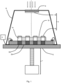
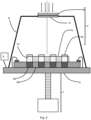
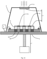
- THE figures 1 And 2 illustrate a multispectral detection device which comprises at least a first photodetector 1a sensitive to a first wavelength range also called first spectral band and a second photodetector 1b sensitive to a second wavelength range also called the second spectral band.
- the first photodetector 1a and the second photodetector 1b comprise a single semiconductor film which is configured to absorb the first wavelength range and the second wavelength range. This embodiment is particularly advantageous because it is very compact.
- first photodetector 1a and the second photodetector 1b each comprise first and second distinct semiconductor films which are respectively configured to detect the first wavelength range and the second wavelength range.
- the multispectral detection device comprises a plurality of first photodetectors and a plurality of second photodetectors.
- the first photodetectors and the second photodetectors form an array. It is particularly advantageous to provide that the first photodetectors and the second photodetectors are uniformly distributed over the detection surface.
- the plurality of first photodetectors and the plurality of second photodetectors form a focal plane array, i.e. all the photodetectors are produced in the same plane.
- the detection device comprises as many first photodetectors as second photodetectors.
- the detection device comprises a number of first photodetectors which is different from the number of second photodetectors.
- the second wavelength range is different from the first wavelength range.
- the second wavelength range is dissociated from the first wavelength range, i.e. the wavelength ranges do not overlap.
- the first and second wavelength ranges have a common terminal or they are separated by an intermediate wavelength range.
- the first photodetector 1a and the second photodetector 1b are both sensitive to the first wavelength range and the second wavelength range.
- the first photodetector 1a and the second photodetector 1b are capable of sensing radiation emitted in the first wavelength range and of providing an electrical signal representative of this radiation.
- the first photodetector 1a and the second photodetector 1b are also capable of sensing radiation emitted in the second wavelength range and of providing an electrical signal representative of this radiation.
- first photodetector 1a and the second photodetector 1b are able to detect the radiation emitted in a third wavelength range which is different from the first and second wavelength ranges.
- This third wavelength range does not contain relevant information, but it makes it possible to facilitate the realization of photodetectors by choosing semiconductor materials that are easier to use.
- the detection device so that it can detect different pairs of wavelength ranges, for example MWIR/LWIR, MWIR/SWIR, LWIR/SWIR, NIR/SWIR, NIR/LWIR or NIR/MWIR.
- the first and second wavelength ranges divide, for example, the MWIR radiation into two distinct sub-ranges.
- the same may apply to LWIR, SWIR or NIR radiation.
- the first and second photodetectors 1a and 1b may be formed by any suitable type of detector, for example by a photodiode, a quantum well detector or a multiple quantum well detector. Other types of photodetectors are also possible.
- the first and second photodetectors 1a and 1b may be implemented in identical or different architectures.
- the first photodetector 1a is identical to the second photodetector 1b, i.e. in materials and in the implementation architecture. It is then much easier to realize the photodetectors in a compact manner.
- the power supply conditions of the photodetectors 1a and 1b may be different.
- the power supply conditions are identical for all the photodetectors.
- the power supply conditions are provided by a first reading circuit 2a for the first photodetector 1a and by a second reading circuit 2b for the second photodetector 1b.
- the photodetectors 1a and 1b and the reading circuits 2a and 2b are advantageously arranged on a support 3.
- the photodetectors are associated with a filtering system 4 of the incident radiation.
- the filtering system 4 is configured so that the first photodetector 1a receives different radiation from the second photodetector 1b. In this way, the two photodetectors 1a and 1b are able to provide two different pieces of information on the observed scene.
- the use of identical photodetectors makes it easier to produce a compact device.
- the compactness is such that it becomes difficult to produce different and efficient filters above the first photodetector 1a and above the second photodetector 1b.
- the filtering system 4 is a dissociated filtering system, that is to say that it comprises at least a first filter 4a and a second filter 4b which have different optical properties and which are arranged successively in the optical path of the first photodetector 1a.
- the first filter 4a and the second filter 4b are not in contact with each other, which makes it possible to facilitate the production of the filtering system 4.
- the first filter 4a has optical and preferably mechanical characteristics different from the second filter 4b.
- the number of layers forming the filter must be increased, which increases the thickness of the filter.
- the increase in thickness is of the order of 2 ⁇ m.
- thermomechanical stresses increase as the thickness increases.
- the filtering system 4 comprises a first filter 4a which is configured to pass the first wavelength range and to block the second wavelength range.
- the first filter 4a may be an interference filter or an absorption filter.
- the first wavelength range may have longer or shorter wavelengths than the second wavelength range.
- the first filter 4a may therefore be a low-pass filter or a high-pass filter whose cut-off wavelength is between the first wavelength range and the second wavelength range. This embodiment is particularly advantageous because the low-pass and high-pass filters are easy to produce, which simplifies their integration on the surface of the photodetectors. They are generally less thick than the other filters.
- the first filter 4a is a band-pass filter which passes the first wavelength range and blocks the second wavelength range.
- This embodiment is slightly less advantageous than the previous one because a band-pass filter is generally thicker than a low-pass or high-pass filter.
- the first filter 4a is a filter which is deposited directly on the first photodetector 1a, that is to say on a part of the focal plane array.
- the first filter 4a is not deposited on the second photodetector 1b so the first filter 4a covers the first photodetector 1a and leaves the second photodetector 1b uncovered.
- the first filter 4a is in physical contact with the first photodetector 1a.
- the first filter 4a makes it possible to limit the crosstalk between the first photodetector 1a and the adjacent second photodetector 1b.
- the first photodetector 1a receives only a part of the incident radiation.
- the first photodetector 1a receives the first wavelength range and it does not receive the second wavelength range.
- the filtering system 4 also comprises a second filter 4b.
- the second filter 4b is used to block a portion of the incident radiation before being captured by the first and second photodetectors 1a and 1b. More precisely, the second filter 4b is used to block a portion of the incident radiation before striking the focal plane and in particular the first filter 4a which will block another portion of the incident radiation.
- the second filter 4b is arranged at a distance from the first photodetector 1a and the second photodetector 1b, that is to say that the second filter 4b is not in direct contact with the first photodetector 1a, nor with the second photodetector 1b.
- the second filter 4b is deposited on a second substrate which is different from the first substrate supporting the first and second photodetectors or on which the first and second photodetectors are formed.
- the second filter 4b may be an interference filter or an absorption filter.
- the first filter 4a and the second filter 4b work in association to filter the radiation received by the first photodetector 1a.
- first filter 4a By separating the first filter 4a and the second filter 4b, it is possible to obtain an overall filter capable of allowing only the relevant radiation to pass towards the first photodetector while limiting the thickness of the first filter 4a formed directly on the first photodetector. In this way, it is possible to form more compact first filters.
- the second filter 4b is separated from the photodetectors 1a and 1b and from the first filter 4a by a layer of gas or vacuum. In this way, the thermomechanical stresses related to the second filter 4b are greatly reduced or even eliminated. It is then easier to form the first filter 4a and the second filter 4b. The thickness of the first filter can be reduced which reduces the thermomechanical stresses.
- the second filter 4b is advantageously transferred to the substrate containing the first photodetector 1a and the second photodetector 1b.
- the second filter 4b can then be formed separately from the first filter 4a and the method of producing the second filter 4b does not interfere with the first filter 4a, nor with the photodetectors 1a and 1b.
- the second filter 4b is advantageously transferred to the support 3 which is configured to support the substrate containing the first photodetector 1a and the second photodetector 1b.
- the second filter 4b can then be formed separately from the first filter 4a and the method of producing the second filter 4b does not interfere with the first filter 4a, nor with the photodetectors 1a and 1b.
- the second filter 4b being arranged at a distance from the first filter 4a and the photodetectors 1a and 1b.
- the second filter 4b is a filter common to the first photodetector 1a and the second photodetector 1b. In this way, the second filter 4b is not linked to an alignment constraint with respect to the first filter 4a, nor to the second photodetector 1b.
- the second filter 4b is located between the radiation source and the first filter 4a as well as between the radiation source and the second photodetector 1b.
- the second filter 4b being arranged at a distance from the first filter 4a and the photodetectors, the manufacturing and integration constraints are reduced in comparison with the devices of the prior art.
- the second filter 4b is configured to pass the first wavelength range and the second wavelength range.
- the second filter 4b is advantageously configured to block the third wavelength range which is different from the first and second wavelength ranges.
- the second filter 4b is a band-stop filter. It is also possible to make a low-pass or high-pass or bi-lobe filter.
- the filtering system 4 prevents certain wavelengths from reaching the first and second photodetectors 1a/1b and from polluting the useful signals received.
- the second photodetector 1b is devoid of a filter arranged in direct contact with its surface. In this configuration, the second photodetector 1b receives the first wavelength and the second wavelength because it is not associated with the first filter 4a. This embodiment is particularly advantageous because only the first photodetector 1a is covered with a first filter 4a which facilitates the production of the detection device with small photodetectors.
- the first photodetector 1a emits an electrical signal that is representative of the radiation received.
- the electrical signal from the first photodetector 1a is representative of radiation in the first wavelength range only.
- the second photodetector 1b also emits an electrical signal that is representative of the radiation received.
- the electrical signal from the second photodetector 1b is representative of the radiation in the first wavelength range and in the second wavelength range.
- the differences in information between the two signals are representative of radiation in the second wavelength range.
- the first photodetector 1a is connected to a reading/processing circuit 5 which receives the first electrical signal.
- the second photodetector 1b is also connected to the reading/processing circuit 5 which receives the second electrical signal.
- the reading/processing circuit 5 is configured to compare the first electrical signal with the second electrical signal and to provide a third signal representative of the radiation received by the second photodetector 1b in the second wavelength range.
- the reading/processing circuit can be produced in the substrate 3. It is also possible to dissociate the reading and processing functions and to produce the reading function in the support 3. The processing function is then carried out separately.
- a second filter 4b which is a high-pass filter or a low-pass filter.
- the second filter 4b is then configured to pass the first wavelength range and the second wavelength range and to block a wavelength greater than the greater of the first and second wavelength ranges or to block the wavelength less than the smaller of the first and second wavelength ranges.
- a second filter 4b which is a bandpass filter whose lower cut-off wavelength and upper cut-off wavelength correspond to the ends of the interval defined by the first and second wavelength ranges. In this way, part of the manufacturing hazards of the photodetectors is eliminated.
- the second filter 4b may be a bi-lobe filter also called dual-band which is more complicated to produce and which is thicker.
- the bi-lobe filter is configured to pass the first wavelength range and the second wavelength range. This filter allows a better selection of the useful wavelengths. The complexity of production and its greater thickness are no longer problems because the filter is offset relative to the photodetectors.
- the second filter 4b allows the first wavelength range and the second wavelength range to pass through and excludes, at least in part or even completely, the radiation in the undesired wavelength ranges.
- this embodiment is particularly advantageous compared to the embodiments of the prior art. Indeed, in the documents of the prior art, it is proposed to produce a first filter on the first photodetector and a second different filter on the second photodetector.
- the two filters used have significant thicknesses which can be of the same order of magnitude as the lateral dimension of the photodetector. It is therefore difficult to properly control the production of a detection matrix with a small pitch between the photodetectors.
- the first filter 4a By using a single filter, here the first filter 4a, to specialize the first photodetectors with respect to the second photodetectors, it is easier to realize a detection matrix with a low repetition pitch.
- the alignment constraints are limited to the first filter 4a in the manufacturing process.
- first filter 4a that is configured to pass the first wavelength range and block the second wavelength range has the advantage of being simple to produce. There are no longer the constraints linked to the subsequent steps of deposition and etching or by lift-off to form another filter on the substrate containing the photodetectors.
- the first filter 4a can be a thin filter and the technological steps for forming this first filter are reduced, which reduces the risks of deterioration of the first and/or second photodetectors.
- the low-pass, high-pass or band-pass filter which is the easiest to produce and/or the thinnest in order to block part of the incident radiation and thus specialize the first photodetector 1a in relation to the second photodetector 1b.
- an anti-reflection layer (not shown) is used.
- the anti-reflection layer can be arranged on the second filter 4b, that is to say that the second filter 4b separates the anti-reflection layer and the photodetectors 1a and 1b.
- the anti-reflection layer is deposited on the second photodetector 1b and on the first filter 4a.
- the anti-reflection layer separates the second filter 4b and the first filter 4a.
- a first anti-reflection layer is deposited on the photodetectors 1a and 1b and a second anti-reflection layer is deposited on the second filter 4b or in contact with the second filter 4b.
- the anti-reflection layer can be deposited on the first filter or between the first photodetector 1a and the first filter 4a.
- the antireflection layer is advantageously configured to allow infrared radiation to pass through.
- a passivation layer is used to cover the first and/or second photodetectors 1a and 1b.
- the passivation layer is arranged between the first photodetector 1a and the first filter 4a.
- the passivation layer has a thickness of between 10 nm and 2000 nm.
- the use of a passivation layer is particularly advantageous for limiting pollution of the unfiltered band. For example, pollution of the unfiltered band can result in contamination with elements external to the device or by the diffusion of contaminants.
- the passivation layer makes it possible to keep contaminants out of the photodetectors and/or out of the filters so as not to modify the optical and/or electrical performances.
- the contaminants are for example gold or copper.
- the detection device comprises a continuous passivation layer which covers the first and second photodetectors 1a and 1b in a monolithic manner.
- the continuous passivation layer allows better management of thermomechanical stresses by smoothing the stresses on the first and second photodetectors. It is particularly advantageous to provide that the material used to form the passivation layer is a material having a low diffusion coefficient of contaminating species.
- a bonding promoter is arranged between the photodetectors and/or filters and the passivation layer.
- the passivation layer is made of a material chosen from Ge, ZnS, CdTe, SiO X , SiN x so as to simultaneously form a passivation layer and an antireflection layer.
- antireflective coating can be made up of a single layer in a single material or by a stack of several layers in different materials.
- the inventors also observed that it is advantageous to use first and second photodetectors that are sensitive to the first wavelength range, the second wavelength range, and are not sensitive between these two wavelength ranges.
- the specialization of the first photodetector 1a with respect to the second photodetector 1b is easy to achieve because the constraint on the cutoff frequency of the first filter 4a is reduced.
- This embodiment is also advantageous because the constraints on the second filter 4b are also reduced.
- the photodetectors are sensitive to at least a third wavelength range that is between the first and second wavelength ranges. It is then advantageous to use a bi-lobe filter.
- the filtering system 4 is configured to block this third wavelength range. More particularly, the third wavelength range is blocked by the second filter 4b.
- the second filter 4b is a high-pass filter that is configured to cut off wavelengths below the lower end of the interval defined by the first and second wavelength ranges.
- a filter makes it possible to block stray radiation that corresponds to wavelengths below the cutoff wavelength and that can be absorbed by the photodetectors 1a and 1b.
- the first filter 4a can be a high-pass filter, a low-pass filter or a band-pass filter.
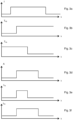
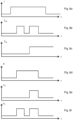
- the first filter 4a is a low-pass filter whose transmission curve is illustrated in figure 3c
- the first wavelength range has shorter wavelengths than the second wavelength range.
- the first photodetector 1a receives only the wavelength range associated with the shorter wavelengths as illustrated with the intensity curve of the figure 3e .
- the second photodetector 1b receives both wavelength ranges as illustrated with the intensity curve of the figure 3f .
- There 3d figure represents the absorption wavelength range of the first and second photodetectors 1a and 1b.
- the first filter 4a is a high-pass filter whose transmission curve is illustrated in figure 4c
- the first wavelength range has longer wavelengths than the second wavelength range.
- the first photodetector 1a receives only the wavelength range wavelength associated with the longest wavelengths as illustrated with the intensity curve of the figure 4e .
- the second photodetector 1b receives both wavelength ranges as illustrated with the intensity curve of the figure 4f .
- There figure 4d represents the absorption wavelength range of the first and second photodetectors 1a and 1b.
- the first wavelength range may have shorter or longer wavelengths than the second wavelength range depending on the characteristics of the first filter 4a. If the first filter 4a is configured to pass the shorter wavelengths then the operation is equivalent to a low-pass filter. If the first filter 4a is configured to pass the longer wavelengths then the operation is equivalent to a high-pass filter.
- the second filter 4b is a low-pass filter that is configured to cut off wavelengths above the upper end of the interval defined by the first and second wavelength ranges.
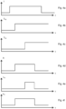
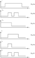
- a filter makes it possible to block stray radiation that corresponds to wavelengths greater than the cut-off wavelength and that can be absorbed by the photodetectors 1a and 1b ( figure 5d ).
- the first filter 4a is a low-pass filter whose transmission curve is illustrated in figure 5c
- the first wavelength range has shorter wavelengths than the second wavelength range.
- the first photodetector 1a receives only the wavelength range wavelength associated with the shortest wavelengths as illustrated with the intensity curve of the figure 5e .
- the second photodetector 1b receives both wavelength ranges as illustrated with the intensity curve of the figure 5f .
- There figure 5d represents the absorption wavelength range of the first and second photodetectors 1a and 1b.
- the first filter 4a is a high-pass filter whose transmission curve is illustrated in figure 6c
- the first wavelength range has longer wavelengths than the second wavelength range.
- the first photodetector 1a receives only the wavelength range associated with the longer wavelengths as illustrated with the intensity curve of the figure 6e .
- the second photodetector 1b receives both wavelength ranges as illustrated with the intensity curve of the figure 6f .
- There figure 6d represents the absorption wavelength range of the first and second photodetectors 1a and 1b.
- the first wavelength range may have shorter or longer wavelengths than the second wavelength range depending on the characteristics of the first filter 4a. If the first filter 4a is configured to pass the shorter wavelengths then the operation is equivalent to a low-pass filter. If the first filter 4a is configured to pass the longer wavelengths then the operation is equivalent to a high-pass filter.
- the second filter 4b is a bandpass filter which is configured to cut off wavelengths below the lower end of the interval defined by the first and second wavelength ranges and to cut off wavelengths above the upper end of the interval defined by the first and second wavelength ranges.
- a filter makes it possible to block parasitic radiation which corresponds to lengths below and above the two cut-off wavelengths and which can be absorbed by the photodetectors 1a and 1b ( figure 7d ).
- the first filter 4a can be a high-pass filter, a low-pass filter or a band-pass filter.
- the first filter 4a is a high-pass filter whose transmission curve is illustrated in figure 7c
- the first wavelength range has longer wavelengths than the second wavelength range.
- the first photodetector 1a receives only the wavelength range associated with the longer wavelengths as illustrated with the intensity curve of the figure 7e .
- the second photodetector 1b receives both wavelength ranges as illustrated with the intensity curve of the figure 7f .
- There figure 7d represents the absorption wavelength range of the first and second photodetectors 1a and 1b.
- the first filter 4a is a low-pass filter (not shown)
- the first wavelength range has shorter wavelengths than the second wavelength range.
- the first photodetector 1a receives only the wavelength range associated with the shorter wavelengths.
- the second photodetector 1b receives both wavelength ranges.
- the first wavelength range may have shorter or longer wavelengths than the second wavelength range depending on the characteristics of the first filter 4a. If the first filter 4a is configured to pass the shorter wavelengths then the operation is equivalent to a low-pass filter. If the first filter 4a is configured to pass the longer wavelengths then the operation is equivalent to a high-pass filter.
- the second filter 4b is a bi-lobe filter whose transmission curve is illustrated in figure 8b
- the bi-lobe filter is associated with a first high-pass filter 4a whose transmission curve is illustrated in figure 8c .
- the first photodetector 1a receives only the wavelength range associated with the longest wavelengths as illustrated with the intensity curve of the figure 8e .
- the second photodetector 1b receives both wavelength ranges as illustrated with the intensity curve of the figure 8f .
- There figure 8d represents the absorption wavelength range of the first and second photodetectors 1a and 1b.
- the first filter 4a may be replaced by a band-pass filter or by a low-pass filter which is illustrated by the Figures 9a to 9f .
- the transmission curve of the low-pass filter is shown in figure 9c .
- the first photodetector 1a receives only the wavelength range associated with the shortest wavelengths as illustrated with the intensity curve of the figure 9e .
- the second photodetector 1b receives both wavelength ranges as illustrated with the intensity curve of the figure 9f .
- There figure 9d represents the wavelength range absorbed by the first and second photodetectors 1a and 1b.
- the second photodetector 1b is covered by a third filter 4c.
- the third filter 4c is configured to pass the second wavelength range and block the first wavelength range.
- the third filter 4c may be an interference filter or an absorption filter.
- the third filter 4c can be a low-pass filter or a high-pass filter whose cutoff wavelength lies between the first wavelength range and the second wavelength range. If the first filter is a low-pass filter, the second filter is a high-pass filter and vice versa.
- the third filter 4c is a band-pass filter which passes the second wavelength range and blocks the first wavelength range.
- This embodiment is less advantageous than the previous one because a band-pass filter is thicker than a low-pass or high-pass filter.
- the third filter 4c is a filter deposited directly on the second photodetector 1b, that is to say on a part of the focal plane array.
- the third filter 4c is not deposited on the first photodetector 1a so the third filter 4c only covers the second photodetector 1b and it leaves the first photodetector 1a uncovered.
- the third filter 4c is in physical contact with the second photodetector.
- the third filter 4c makes it possible to limit the crosstalk between the first photodetector 1a and the adjacent second photodetector 1b.
- the second photodetector 1b receives only a part of the incident radiation.
- the second photodetector 1b receives the second wavelength range and it does not receive the first wavelength range.
- Each photodetector provides information representative of the observed wavelength range.
- the processing circuit can be simplified because it is no longer necessary to compare the signals from the two photodetectors.
- the emission curve of the observed scene extends beyond the first and second wavelength ranges.
- the detection device can be simply realized in the following manner.
- the first photodetector 1a and the second photodetector 1b are formed on a semiconductor substrate. Since the two photodetectors 1a and 1b are sensitive to the same wavelength ranges, it is advantageous to realize the two photodetectors simultaneously and with the same semiconductor materials. In a preferred embodiment, the photodetectors 1a and 1b are identical.
- the two photodetectors are offset along an axis parallel to the plane of the substrate surface and they are in the same plane which is parallel to the plane of the substrate surface.
- a first filter 4a is formed on the first photodetector 1a so as to cover the first photodetector 1a and to leave the second photodetector 1b uncovered.
- the first filter 4a is formed on the first photodetector 1a and on the second photodetector 1b. The first filter 4a is then removed above the second photodetector 1b.
- the second photodetector 1b is protected by a sacrificial layer.
- the first filter 4a is formed on the first photodetector 1a and on the sacrificial layer.
- the sacrificial layer is removed so as to release the second photodetector 1b which is devoid of a first filter.
- the second filter 4b is associated, for example brought into contact, with the substrate containing the first photodetector 1a and the second photodetector 1b.
- the second filter 4b is not formed by deposition on the substrate, it was formed independently and it is reported subsequently.
- the first filter 4a can be formed before or after the third filter 4c. It is also possible to provide that the first filter 4a and the third filter 4c are formed partly simultaneously by sharing some layers.
- the third filter 4c is produced before installing the second filter 4b. the third filter 4c is arranged at a distance from the second filter 4b.
- first and second photodetectors 1a and 1b in a closed enclosure that is advantageously sealed.
- This closed enclosure includes an orifice configured to allow radiation to pass from the radiation source to the first and second photodetectors 1a and 1b.
- the second filter 4b in this orifice so as to allow the first and second wavelength ranges to pass and to block a portion of the unnecessary radiation.
- the orifice is advantageously a window 6 made of transparent material covered by the second filter 4b.
- the second filter 4b may be located inside the closed enclosure ( figure 1 ) or outside the closed enclosure ( figure 2 ). The entire surface of the window is advantageously covered by the second filter 4b in order to leave only the useful signal in all areas of the window.
- the detection device is a cooled detection device, i.e. a device that is configured to operate at a temperature below 300K, preferably between 40K and 300K and preferably below 200K.
- the detection device may also be uncooled.
- the detection device is advantageously coupled to a cooling system 7 which allows it to be cooled to its operating temperature.
- the photodetectors of the detection device can be made of II-VI material, for example HgCdTe or of III-V material, for example InGaAs, InSb, InAsSb.
- the photodetectors 1a and 1b are advantageously surrounded by a cold screen 8 which is configured to block the incident radiation with the exception of the window 6 for the passage of the incident radiation. It appears particularly advantageous to place the second filter 4b on this window 6 for the passage of the incident radiation.
- the areas covered by the first filter 4a and the areas left uncovered by the first filter 4a advantageously define an alternation between the first photodetectors 1a and the second photodetectors 1b.
- This alternation between the first and second photodetectors can result in the creation of a checkerboard or an alternation of bands represented by rows or columns of photodetectors.
- the pressure inside the cold screen 8 is less than or equal to the pressure outside the cold screen 8. It is advantageous to provide that the pressure inside the cold screen 8 is lower than atmospheric pressure, for example lower than 1013hPa.
- the pressure inside the cold shield is less than 10 -4 Pa.
Landscapes
- Photometry And Measurement Of Optical Pulse Characteristics (AREA)
- Physics & Mathematics (AREA)
- Spectroscopy & Molecular Physics (AREA)
- Spectrometry And Color Measurement (AREA)
- Solid State Image Pick-Up Elements (AREA)
- Color Television Image Signal Generators (AREA)
- Light Receiving Elements (AREA)
- Measurement And Recording Of Electrical Phenomena And Electrical Characteristics Of The Living Body (AREA)
- Investigating Or Analysing Materials By Optical Means (AREA)
- Measurement Of Resistance Or Impedance (AREA)
Claims (11)
- Multispektrale Detektionsvorrichtung, umfassend:- einen ersten Fotodetektor (1a) und einen zweiten Fotodetektor (1b), die jeweils gegenüber einem ersten Wellenlängenbereich und einem zweiten Wellenlängenbereich, der sich vom ersten Wellenlängenbereich unterscheidet, empfindlich sind, wobei der erste Fotodetektor (1a) ein erstes Signal ausgibt, das für die empfangene Strahlung repräsentativ ist, und der zweite Fotodetektor (1b) ein zweites Signal ausgibt, das für die empfangene Strahlung repräsentativ ist,- einen ersten Filter (4a), der dazu konfiguriert ist, den ersten Wellenlängenbereich durchzulassen und den zweiten Wellenlängenbereich zu blockieren, wobei der erste Filter (4a) den ersten Fotodetektor (1a) bedeckt und den zweiten Fotodetektor (1b) unbedeckt lässt, der erste Filter (4a) derart auf dem ersten Fotodetektor (1a) angeordnet ist, dass der Durchgang des zweiten Wellenlängenbereichs in den ersten Fotodetektor (1a) blockiert wird und im ersten Fotodetektor (1a) und im zweiten Fotodetektor (1b) thermomechanische Beanspruchungen erzeugt werden,- einen zweiten Filter (4b), der beabstandet vom ersten und vom zweiten Fotodetektor (1a, 1b) und beabstandet vom ersten Filter (4a) angeordnet ist, wobei der zweite Filter (4b) dazu konfiguriert ist, den ersten Wellenlängenbereich und den zweiten Wellenlängenbereich durchzulassen, der zweite Filter (4b) dazu konfiguriert ist, eine Wellenlänge zu blockieren, die größer ist als die längste der Wellenlängen des ersten und zweiten Wellenlängenbereichs, und/oder eine Wellenlänge zu blockieren, die kleiner ist als die kürzeste der Wellenlängen des ersten und zweiten Wellenlängenbereichs, wobei der erste Filter (4a) und der zweite Filter (4b) im Lichtweg des ersten Fotodetektors (1a) aufeinanderfolgend angeordnet sind, wobei der zweite Filter (4b) dem ersten Fotodetektor (1a) und dem zweiten Fotodetektor (1b) gemeinsam ist,wobei die multispektrale Detektionsvorrichtung dadurch gekennzeichnet ist, dass der erste und der zweite Wellenlängenbereich Bereiche der Infrarotstrahlung sind, und dass sie umfasst:- eine durchgehende Passivierungsschicht, die den ersten und den zweiten Fotodetektor (1a, 1b) monolithisch bedeckt und zwischen dem ersten Fotodetektor (1a) und dem ersten Filter (4a) angeordnet ist, wobei die Passivierungsschicht eine Dicke zwischen 10 nm und 2000 nm aufweist, um die thermomechanischen Beanspruchungen auf dem ersten und dem zweiten Fotodetektor (1a, 1b) zu glätten.
- Detektionsvorrichtung nach Anspruch 1, wobei der zweite Fotodetektor (1b) mit keinem Filter versehen ist, der dazu konfiguriert ist, den ersten Wellenlängenbereich zu blockieren, sodass er den ersten Wellenlängenbereich und den zweiten Wellenlängenbereich empfängt, wobei die Detektionsvorrichtung eine Verarbeitungsschaltung (5) umfasst, die dazu konfiguriert ist, vom ersten und vom zweiten Fotodetektor (1a, 1b) elektrische Signale zu empfangen und durch Vergleichen des ersten Signals mit dem zweiten Signal eine Information bezüglich der Strahlung des zweiten Wellenlängenbereichs bereitzustellen.
- Detektionsvorrichtung nach Anspruch 1, wobei der zweite Fotodetektor (1b) von einem dritten Filter (4c) bedeckt ist, der dazu konfiguriert ist, den ersten Wellenlängenbereich zu blockieren und den zweiten Wellenlängenbereich durchzulassen.
- Detektionsvorrichtung nach einem der vorherigen Ansprüche, dadurch gekennzeichnet, dass der zweite Filter (4b) aus einem Tiefpass-, Hochpass-, Bandpass- und Dualbandfilter gewählt ist.
- Detektionsvorrichtung nach einem der vorherigen Ansprüche, dadurch gekennzeichnet, dass der erste Filter (4a) ein Tiefpass-, Hochpass- oder Bandpassfilter ist, der den zweiten Wellenlängenbereich abschneidet.
- Detektorvorrichtung nach einem der vorherigen Ansprüche, dadurch gekennzeichnet, dass der zweite Filter (4b) durch eine Gasschicht oder ein Vakuum vom ersten Filter (4a) und vom zweiten Photodetektor (1b) beabstandet angeordnet ist.
- Detektionsvorrichtung nach einem der vorherigen Ansprüche, dadurch gekennzeichnet, dass sie einen Kälteschirm (8) umfasst, der dazu konfiguriert ist, die einfallende Strahlung durch eine Durchgangsöffnung für die Strahlung zu fokussieren, und dass der zweite Filter (4b) in dieser Öffnung angeordnet ist.
- Detektionsvorrichtung nach Anspruch 7, dadurch gekennzeichnet, dass der Kälteschirm (8) ein geschlossenes Gehäuse definiert, das den ersten und den zweiten Fotodetektor (1a, 1b) enthält, und dass der zweite Filter (4b) im geschlossenen Raum angeordnet ist.
- Detektionsvorrichtung nach Anspruch 7, dadurch gekennzeichnet, dass der Kälteschirm (8) ein geschlossenes Gehäuse definiert, das den ersten und den zweiten Fotodetektor (1a, 1b) enthält, und dass der zweite Filter (4b) außerhalb des geschlossenen Gehäuses angeordnet ist.
- Verfahren zur Herstellung einer multispektralen Detektionsvorrichtung, umfassend:- Bereitstellen eines Substrats, das einen ersten und einen zweiten Fotodetektor (1a und 1b) und eine durchgehende Passivierungsschicht umfasst, die den ersten und den zweiten Fotodetektor (1a, 1b) monolithisch bedeckt, wobei die Passivierungsschicht eine Dicke zwischen 10 nm und 2000 nm aufweist, wobei der erste und der zweite Fotodetektor (1a, 1b) jeweils gegenüber einem ersten Wellenlängenbereich und einen zweiten Wellenlängenbereich, der sich vom ersten Wellenlängenbereich unterscheidet, empfindlich sind, wobei der erste Fotodetektor (1a) ein erstes Signal ausgibt, das für die empfangene Strahlung repräsentativ ist, und der zweite Fotodetektor (1b) ein zweites Signal ausgibt, das für die empfangene Strahlung repräsentativ ist, wobei der erste und der zweite Wellenlängenbereich Bereiche der Infrarotstrahlung sind,- Bilden eines ersten Filters (4a), der dazu konfiguriert ist, den ersten Wellenlängenbereich durchzulassen und den zweiten Wellenlängenbereich zu blockieren, wobei der erste Filter (4a) den ersten Fotodetektor (1a) bedeckt und den zweiten Fotodetektor (1b) unbedeckt lässt, der erste Filter (4a) derart auf dem ersten Fotodetektor (1a) angeordnet ist, dass er den Durchgang des zweiten Wellenlängenbereichs in den ersten Fotodetektor (1a) blockiert, der erste Filter (4a) durch die Passivierungsschicht vom ersten Fotodetektor (1a) getrennt ist, der erste Filter (4a) im ersten Fotodetektor (1a) und im zweiten Fotodetektor (1b) thermomechanische Beanspruchungen erzeugt,- Bilden eines zweiten Filters (4b), der beabstandet vom ersten und vom zweiten Fotodetektor (1a, 1b) und beabstandet vom ersten Filter (4a) angeordnet ist, wobei der zweite Filter (4b) dazu konfiguriert ist, den ersten Wellenlängenbereich und den zweiten Wellenlängenbereich durchzulassen, der zweite Filter (4b) dazu konfiguriert ist, eine Wellenlänge zu blockieren, die größer ist als die längste der Wellenlängen des ersten und zweiten Wellenlängenbereichs, und/oder eine Wellenlänge zu blockieren, die kleiner ist als die kürzeste der Wellenlängen des ersten und zweiten Wellenlängenbereichs, wobei der erste Filter (4a) und der zweite Filter (4b) im Lichtweg des ersten Fotodetektors (1a) aufeinanderfolgend angeordnet sind, der zweite Filter (4b) dem ersten Fotodetektor (1a) und dem zweiten Fotodetektor (1b) gemeinsam ist, wobei die Passivierungsschicht die thermomechanischen Beanspruchungen auf dem ersten und dem zweiten Fotodetektor (1a, 1b) glättet.
- Herstellungsverfahren nach Anspruch 10, umfassend, vor dem Bilden des zweiten Filters (4b):- Bilden eines dritten Filters (4c), der dazu konfiguriert ist, den zweiten Wellenlängenbereich durchzulassen und den ersten Wellenlängenbereich zu blockieren, wobei der dritte Filter (4c) den zweiten Fotodetektor (1b) bedeckt und den ersten Fotodetektor (1a) unbedeckt lässt, wobei der dritte Filter (4c) derart mit dem zweiten Fotodetektor (1b) in Kontakt ist, dass er den Durchgang des ersten Wellenlängenbereichs in den zweiten Fotodetektor (1b) blockiert.
Applications Claiming Priority (2)
| Application Number | Priority Date | Filing Date | Title |
|---|---|---|---|
| FR1662090A FR3059823B1 (fr) | 2016-12-07 | 2016-12-07 | Dispositif de detection multispectrale ameliore. |
| PCT/FR2017/053405 WO2018104655A1 (fr) | 2016-12-07 | 2017-12-05 | Dispositif de detection multispectrale ameliore |
Publications (2)
| Publication Number | Publication Date |
|---|---|
| EP3552237A1 EP3552237A1 (de) | 2019-10-16 |
| EP3552237B1 true EP3552237B1 (de) | 2025-01-22 |
Family
ID=58707627
Family Applications (1)
| Application Number | Title | Priority Date | Filing Date |
|---|---|---|---|
| EP17816992.6A Active EP3552237B1 (de) | 2016-12-07 | 2017-12-05 | Vorrichtung zur verbesserten multispektralen erkennung |
Country Status (8)
| Country | Link |
|---|---|
| US (1) | US11302729B2 (de) |
| EP (1) | EP3552237B1 (de) |
| JP (1) | JP7161267B2 (de) |
| KR (1) | KR102470061B1 (de) |
| CN (1) | CN110235252B (de) |
| FR (1) | FR3059823B1 (de) |
| IL (1) | IL267147B2 (de) |
| WO (1) | WO2018104655A1 (de) |
Families Citing this family (3)
| Publication number | Priority date | Publication date | Assignee | Title |
|---|---|---|---|---|
| FR3084523B1 (fr) * | 2018-07-27 | 2020-12-25 | Soc Fr De Detecteurs Infrarouges Sofradir | Dispositif de detection electromagnetique |
| CN116358697A (zh) * | 2021-12-27 | 2023-06-30 | 北京小米移动软件有限公司 | 环境光传感器、环境光检测方法及装置、终端设备及介质 |
| CN115371807B (zh) * | 2022-07-27 | 2025-09-23 | 海南空天信息研究院 | 一种阵列相干平衡光电探测组件及制造方法 |
Citations (1)
| Publication number | Priority date | Publication date | Assignee | Title |
|---|---|---|---|---|
| US20050189492A1 (en) * | 2004-02-26 | 2005-09-01 | Milton A. F. | Multi-color infrared imaging device |
Family Cites Families (35)
| Publication number | Priority date | Publication date | Assignee | Title |
|---|---|---|---|---|
| JPS57204995A (en) * | 1981-06-12 | 1982-12-15 | Sanyo Electric Co | Pyroelectric infrared rays detector |
| JPS6136906Y2 (de) * | 1985-12-25 | 1986-10-25 | ||
| US4996427A (en) * | 1989-12-26 | 1991-02-26 | General Electric Company | Imager for simultaneously obtaining two images of differing color bands using a single photodetector area array |
| JPH0416330U (de) * | 1990-05-31 | 1992-02-10 | ||
| CA2084789A1 (en) * | 1990-06-09 | 1991-12-10 | Bernadette L. A. Ward | Light detector |
| US5258618A (en) * | 1991-12-12 | 1993-11-02 | General Electric Company | Infrared imager forming two narrow waveband images of the same object field |
| JPH0581667U (ja) * | 1992-03-31 | 1993-11-05 | 国際技術開発株式会社 | 赤外線受光装置 |
| FR2737566B1 (fr) * | 1995-08-02 | 1997-09-19 | Sofradir | Procede pour realiser l'assemblage d'un bloc de detection d'ondes electromagnetiques, notamment infrarouges, avec un support conducteur thermique, et detecteur d'ondes electromagnetiques mettant en oeuvre ce procede |
| IL132035A0 (en) * | 1999-09-23 | 2001-03-19 | Israel State | Infrared detector |
| JP4920671B2 (ja) * | 1999-12-28 | 2012-04-18 | ホーチキ株式会社 | 炎検出装置 |
| US7279353B2 (en) * | 2003-04-02 | 2007-10-09 | Micron Technology, Inc. | Passivation planarization |
| US7924483B2 (en) * | 2006-03-06 | 2011-04-12 | Smith Scott T | Fused multi-array color image sensor |
| US7655911B2 (en) * | 2007-04-19 | 2010-02-02 | Drs Sensors & Targeting Systems, Inc. | Image sensor having a variable aperture and mono-color focal plane array for dual color detection |
| KR100877069B1 (ko) * | 2007-04-23 | 2009-01-09 | 삼성전자주식회사 | 이미지 촬상 장치 및 방법 |
| KR101475464B1 (ko) * | 2008-05-09 | 2014-12-22 | 삼성전자 주식회사 | 적층형 이미지 센서 |
| US8084739B2 (en) * | 2008-07-16 | 2011-12-27 | Infrared Newco., Inc. | Imaging apparatus and methods |
| US8686365B2 (en) * | 2008-07-28 | 2014-04-01 | Infrared Newco, Inc. | Imaging apparatus and methods |
| EP2180513A1 (de) * | 2008-10-27 | 2010-04-28 | Stmicroelectronics SA | Sensor für Nahinfrarot-/Farbbilder |
| KR20110061677A (ko) * | 2009-12-02 | 2011-06-10 | 삼성전자주식회사 | 영상 센서 및 이의 제조 방법. |
| US8559113B2 (en) | 2009-12-10 | 2013-10-15 | Raytheon Company | Multi-spectral super-pixel filters and methods of formation |
| US8408821B2 (en) * | 2010-10-12 | 2013-04-02 | Omnivision Technologies, Inc. | Visible and infrared dual mode imaging system |
| GB201020023D0 (en) * | 2010-11-25 | 2011-01-12 | St Microelectronics Ltd | Radiation sensor |
| US8749636B2 (en) * | 2011-07-12 | 2014-06-10 | Lockheed Martin Corporation | Passive multi-band aperture filters and cameras therefrom |
| US9143704B2 (en) * | 2012-01-20 | 2015-09-22 | Htc Corporation | Image capturing device and method thereof |
| FR2999338B1 (fr) * | 2012-12-10 | 2017-12-08 | Soc Fr De Detecteurs Infrarouges - Sofradir | Imageur monolithique multispectral visible et infrarouge |
| CN108572409B (zh) * | 2013-01-29 | 2022-03-01 | 唯亚威通讯技术有限公司 | 可变滤光器及基于此的波长选择传感器 |
| FR3008825B1 (fr) * | 2013-07-18 | 2016-12-09 | Soc Francaise De Detecteurs Infrarouges - Sofradir | Doigt froid ameliore et dispositif de detection comportant le doigt froid |
| CN203883014U (zh) | 2014-04-11 | 2014-10-15 | 武汉高德红外股份有限公司 | 一种基于红外滤波的红外双色探测器 |
| FR3022396B1 (fr) | 2014-06-13 | 2016-07-22 | Sagem Defense Securite | Capteur matriciel bispectral et son procede de fabrication |
| US9374538B2 (en) * | 2014-09-15 | 2016-06-21 | Taiwan Semiconductor Manufacturing Co., Ltd. | Image sensor with embedded infrared filter layer |
| US9570491B2 (en) * | 2014-10-08 | 2017-02-14 | Omnivision Technologies, Inc. | Dual-mode image sensor with a signal-separating color filter array, and method for same |
| WO2016088644A1 (ja) * | 2014-12-04 | 2016-06-09 | Jsr株式会社 | 固体撮像装置 |
| US20170034456A1 (en) * | 2015-07-31 | 2017-02-02 | Dual Aperture International Co., Ltd. | Sensor assembly with selective infrared filter array |
| DE102016105579A1 (de) * | 2016-03-24 | 2017-09-28 | Connaught Electronics Ltd. | Optisches Filter für eine Kamera eines Kraftfahrzeugs, Kamera für ein Fahrerassistenzsystem, Fahrerassistenzsystem sowie Kraftfahrzug mit einem Fahrerassistensystem |
| US11002607B2 (en) * | 2019-04-01 | 2021-05-11 | Raytheon Company | Direct mounting of filters or other optical components to optical detectors using flexures |
-
2016
- 2016-12-07 FR FR1662090A patent/FR3059823B1/fr active Active
-
2017
- 2017-12-05 WO PCT/FR2017/053405 patent/WO2018104655A1/fr not_active Ceased
- 2017-12-05 KR KR1020197019068A patent/KR102470061B1/ko active Active
- 2017-12-05 JP JP2019530415A patent/JP7161267B2/ja active Active
- 2017-12-05 US US16/465,877 patent/US11302729B2/en active Active
- 2017-12-05 EP EP17816992.6A patent/EP3552237B1/de active Active
- 2017-12-05 CN CN201780084974.4A patent/CN110235252B/zh active Active
-
2019
- 2019-06-06 IL IL267147A patent/IL267147B2/en unknown
Patent Citations (1)
| Publication number | Priority date | Publication date | Assignee | Title |
|---|---|---|---|---|
| US20050189492A1 (en) * | 2004-02-26 | 2005-09-01 | Milton A. F. | Multi-color infrared imaging device |
Also Published As
| Publication number | Publication date |
|---|---|
| IL267147B2 (en) | 2023-05-01 |
| US20190296068A1 (en) | 2019-09-26 |
| WO2018104655A1 (fr) | 2018-06-14 |
| JP2020501152A (ja) | 2020-01-16 |
| FR3059823A1 (fr) | 2018-06-08 |
| KR20190091322A (ko) | 2019-08-05 |
| KR102470061B1 (ko) | 2022-11-22 |
| CN110235252A (zh) | 2019-09-13 |
| IL267147A (en) | 2019-08-29 |
| JP7161267B2 (ja) | 2022-10-26 |
| US11302729B2 (en) | 2022-04-12 |
| EP3552237A1 (de) | 2019-10-16 |
| CN110235252B (zh) | 2023-08-22 |
| FR3059823B1 (fr) | 2019-08-23 |
| IL267147B1 (en) | 2023-01-01 |
Similar Documents
| Publication | Publication Date | Title |
|---|---|---|
| EP2636068B1 (de) | Monolithischer multispektraler bildgeber im sichtbaren und nahinfrarot-bereich | |
| EP2636067B1 (de) | Detektor für sichtbare und nahinfrarot-strahlung | |
| EP2636066B1 (de) | Detektor für sichtbare und nahinfrarot-strahlung | |
| EP3449228B1 (de) | Multispektrale bildgebungsvorrichtung | |
| EP2693242B1 (de) | Optische Filterstruktur für sichtbaren und/oder infraroten Spektralbereich | |
| EP3830535B1 (de) | Multispektraler bildsensor mit mitteln zur nebensprechbegrenzung | |
| EP2786412B1 (de) | Optische detektoreinheit | |
| US20190006406A1 (en) | Imaging element and camera system | |
| EP3155660B1 (de) | Bispektraler matrixsensor und verfahren zur herstellung davon | |
| FR3059823B1 (fr) | Dispositif de detection multispectrale ameliore. | |
| EP3465112B1 (de) | Verfahren zur begrenzung von nebensprechen in einem bildsensor | |
| EP3471151B1 (de) | Helmholtz-resonator-photodetektor | |
| EP3190621B1 (de) | Hybrid-vorrichtung zur multispektralen erkennung anhand von monolithischen elementen | |
| EP3830873B1 (de) | Vorrichtung zur erkennung von elektromagnetischer strahlung | |
| FR3139412A1 (fr) | Capteur d’images | |
| FR3163770A1 (fr) | Dispositif électronique ayant des pixels à base de boîtes quantiques | |
| WO2022129791A1 (fr) | Photodétecteur multispectral infrarouge |
Legal Events
| Date | Code | Title | Description |
|---|---|---|---|
| STAA | Information on the status of an ep patent application or granted ep patent |
Free format text: STATUS: UNKNOWN |
|
| STAA | Information on the status of an ep patent application or granted ep patent |
Free format text: STATUS: THE INTERNATIONAL PUBLICATION HAS BEEN MADE |
|
| PUAI | Public reference made under article 153(3) epc to a published international application that has entered the european phase |
Free format text: ORIGINAL CODE: 0009012 |
|
| STAA | Information on the status of an ep patent application or granted ep patent |
Free format text: STATUS: REQUEST FOR EXAMINATION WAS MADE |
|
| 17P | Request for examination filed |
Effective date: 20190615 |
|
| AK | Designated contracting states |
Kind code of ref document: A1 Designated state(s): AL AT BE BG CH CY CZ DE DK EE ES FI FR GB GR HR HU IE IS IT LI LT LU LV MC MK MT NL NO PL PT RO RS SE SI SK SM TR |
|
| AX | Request for extension of the european patent |
Extension state: BA ME |
|
| DAV | Request for validation of the european patent (deleted) | ||
| DAX | Request for extension of the european patent (deleted) | ||
| STAA | Information on the status of an ep patent application or granted ep patent |
Free format text: STATUS: EXAMINATION IS IN PROGRESS |
|
| 17Q | First examination report despatched |
Effective date: 20210628 |
|
| GRAP | Despatch of communication of intention to grant a patent |
Free format text: ORIGINAL CODE: EPIDOSNIGR1 |
|
| STAA | Information on the status of an ep patent application or granted ep patent |
Free format text: STATUS: GRANT OF PATENT IS INTENDED |
|
| INTG | Intention to grant announced |
Effective date: 20240719 |
|
| GRAJ | Information related to disapproval of communication of intention to grant by the applicant or resumption of examination proceedings by the epo deleted |
Free format text: ORIGINAL CODE: EPIDOSDIGR1 |
|
| STAA | Information on the status of an ep patent application or granted ep patent |
Free format text: STATUS: EXAMINATION IS IN PROGRESS |
|
| GRAP | Despatch of communication of intention to grant a patent |
Free format text: ORIGINAL CODE: EPIDOSNIGR1 |
|
| STAA | Information on the status of an ep patent application or granted ep patent |
Free format text: STATUS: GRANT OF PATENT IS INTENDED |
|
| INTC | Intention to grant announced (deleted) | ||
| INTG | Intention to grant announced |
Effective date: 20240925 |
|
| GRAS | Grant fee paid |
Free format text: ORIGINAL CODE: EPIDOSNIGR3 |
|
| GRAA | (expected) grant |
Free format text: ORIGINAL CODE: 0009210 |
|
| STAA | Information on the status of an ep patent application or granted ep patent |
Free format text: STATUS: THE PATENT HAS BEEN GRANTED |
|
| AK | Designated contracting states |
Kind code of ref document: B1 Designated state(s): AL AT BE BG CH CY CZ DE DK EE ES FI FR GB GR HR HU IE IS IT LI LT LU LV MC MK MT NL NO PL PT RO RS SE SI SK SM TR |
|
| REG | Reference to a national code |
Ref country code: GB Ref legal event code: FG4D Free format text: NOT ENGLISH |
|
| REG | Reference to a national code |
Ref country code: CH Ref legal event code: EP |
|
| REG | Reference to a national code |
Ref country code: IE Ref legal event code: FG4D Free format text: LANGUAGE OF EP DOCUMENT: FRENCH |
|
| REG | Reference to a national code |
Ref country code: DE Ref legal event code: R096 Ref document number: 602017087456 Country of ref document: DE |
|
| REG | Reference to a national code |
Ref country code: NL Ref legal event code: MP Effective date: 20250122 |
|
| PG25 | Lapsed in a contracting state [announced via postgrant information from national office to epo] |
Ref country code: NL Free format text: LAPSE BECAUSE OF FAILURE TO SUBMIT A TRANSLATION OF THE DESCRIPTION OR TO PAY THE FEE WITHIN THE PRESCRIBED TIME-LIMIT Effective date: 20250122 |
|
| PG25 | Lapsed in a contracting state [announced via postgrant information from national office to epo] |
Ref country code: RS Free format text: LAPSE BECAUSE OF FAILURE TO SUBMIT A TRANSLATION OF THE DESCRIPTION OR TO PAY THE FEE WITHIN THE PRESCRIBED TIME-LIMIT Effective date: 20250422 |
|
| PG25 | Lapsed in a contracting state [announced via postgrant information from national office to epo] |
Ref country code: FI Free format text: LAPSE BECAUSE OF FAILURE TO SUBMIT A TRANSLATION OF THE DESCRIPTION OR TO PAY THE FEE WITHIN THE PRESCRIBED TIME-LIMIT Effective date: 20250122 |
|
| PG25 | Lapsed in a contracting state [announced via postgrant information from national office to epo] |
Ref country code: PL Free format text: LAPSE BECAUSE OF FAILURE TO SUBMIT A TRANSLATION OF THE DESCRIPTION OR TO PAY THE FEE WITHIN THE PRESCRIBED TIME-LIMIT Effective date: 20250122 |
|
| PG25 | Lapsed in a contracting state [announced via postgrant information from national office to epo] |
Ref country code: ES Free format text: LAPSE BECAUSE OF FAILURE TO SUBMIT A TRANSLATION OF THE DESCRIPTION OR TO PAY THE FEE WITHIN THE PRESCRIBED TIME-LIMIT Effective date: 20250122 |
|
| REG | Reference to a national code |
Ref country code: LT Ref legal event code: MG9D |
|
| PG25 | Lapsed in a contracting state [announced via postgrant information from national office to epo] |
Ref country code: IS Free format text: LAPSE BECAUSE OF FAILURE TO SUBMIT A TRANSLATION OF THE DESCRIPTION OR TO PAY THE FEE WITHIN THE PRESCRIBED TIME-LIMIT Effective date: 20250522 Ref country code: NO Free format text: LAPSE BECAUSE OF FAILURE TO SUBMIT A TRANSLATION OF THE DESCRIPTION OR TO PAY THE FEE WITHIN THE PRESCRIBED TIME-LIMIT Effective date: 20250422 |
|
| REG | Reference to a national code |
Ref country code: AT Ref legal event code: MK05 Ref document number: 1762124 Country of ref document: AT Kind code of ref document: T Effective date: 20250122 |
|
| PG25 | Lapsed in a contracting state [announced via postgrant information from national office to epo] |
Ref country code: HR Free format text: LAPSE BECAUSE OF FAILURE TO SUBMIT A TRANSLATION OF THE DESCRIPTION OR TO PAY THE FEE WITHIN THE PRESCRIBED TIME-LIMIT Effective date: 20250122 |
|
| PG25 | Lapsed in a contracting state [announced via postgrant information from national office to epo] |
Ref country code: LV Free format text: LAPSE BECAUSE OF FAILURE TO SUBMIT A TRANSLATION OF THE DESCRIPTION OR TO PAY THE FEE WITHIN THE PRESCRIBED TIME-LIMIT Effective date: 20250122 Ref country code: PT Free format text: LAPSE BECAUSE OF FAILURE TO SUBMIT A TRANSLATION OF THE DESCRIPTION OR TO PAY THE FEE WITHIN THE PRESCRIBED TIME-LIMIT Effective date: 20250522 |
|
| PG25 | Lapsed in a contracting state [announced via postgrant information from national office to epo] |
Ref country code: GR Free format text: LAPSE BECAUSE OF FAILURE TO SUBMIT A TRANSLATION OF THE DESCRIPTION OR TO PAY THE FEE WITHIN THE PRESCRIBED TIME-LIMIT Effective date: 20250423 Ref country code: BG Free format text: LAPSE BECAUSE OF FAILURE TO SUBMIT A TRANSLATION OF THE DESCRIPTION OR TO PAY THE FEE WITHIN THE PRESCRIBED TIME-LIMIT Effective date: 20250122 |
|
| PG25 | Lapsed in a contracting state [announced via postgrant information from national office to epo] |
Ref country code: AT Free format text: LAPSE BECAUSE OF FAILURE TO SUBMIT A TRANSLATION OF THE DESCRIPTION OR TO PAY THE FEE WITHIN THE PRESCRIBED TIME-LIMIT Effective date: 20250122 |
|
| PG25 | Lapsed in a contracting state [announced via postgrant information from national office to epo] |
Ref country code: SE Free format text: LAPSE BECAUSE OF FAILURE TO SUBMIT A TRANSLATION OF THE DESCRIPTION OR TO PAY THE FEE WITHIN THE PRESCRIBED TIME-LIMIT Effective date: 20250122 |
|
| PG25 | Lapsed in a contracting state [announced via postgrant information from national office to epo] |
Ref country code: SM Free format text: LAPSE BECAUSE OF FAILURE TO SUBMIT A TRANSLATION OF THE DESCRIPTION OR TO PAY THE FEE WITHIN THE PRESCRIBED TIME-LIMIT Effective date: 20250122 |
|
| PG25 | Lapsed in a contracting state [announced via postgrant information from national office to epo] |
Ref country code: DK Free format text: LAPSE BECAUSE OF FAILURE TO SUBMIT A TRANSLATION OF THE DESCRIPTION OR TO PAY THE FEE WITHIN THE PRESCRIBED TIME-LIMIT Effective date: 20250122 |
|
| PG25 | Lapsed in a contracting state [announced via postgrant information from national office to epo] |
Ref country code: IT Free format text: LAPSE BECAUSE OF FAILURE TO SUBMIT A TRANSLATION OF THE DESCRIPTION OR TO PAY THE FEE WITHIN THE PRESCRIBED TIME-LIMIT Effective date: 20250122 |
|
| PG25 | Lapsed in a contracting state [announced via postgrant information from national office to epo] |
Ref country code: EE Free format text: LAPSE BECAUSE OF FAILURE TO SUBMIT A TRANSLATION OF THE DESCRIPTION OR TO PAY THE FEE WITHIN THE PRESCRIBED TIME-LIMIT Effective date: 20250122 Ref country code: CZ Free format text: LAPSE BECAUSE OF FAILURE TO SUBMIT A TRANSLATION OF THE DESCRIPTION OR TO PAY THE FEE WITHIN THE PRESCRIBED TIME-LIMIT Effective date: 20250122 |
|
| REG | Reference to a national code |
Ref country code: DE Ref legal event code: R097 Ref document number: 602017087456 Country of ref document: DE |
|
| PG25 | Lapsed in a contracting state [announced via postgrant information from national office to epo] |
Ref country code: RO Free format text: LAPSE BECAUSE OF FAILURE TO SUBMIT A TRANSLATION OF THE DESCRIPTION OR TO PAY THE FEE WITHIN THE PRESCRIBED TIME-LIMIT Effective date: 20250122 |
|
| PG25 | Lapsed in a contracting state [announced via postgrant information from national office to epo] |
Ref country code: SK Free format text: LAPSE BECAUSE OF FAILURE TO SUBMIT A TRANSLATION OF THE DESCRIPTION OR TO PAY THE FEE WITHIN THE PRESCRIBED TIME-LIMIT Effective date: 20250122 |
|
| PLBE | No opposition filed within time limit |
Free format text: ORIGINAL CODE: 0009261 |
|
| STAA | Information on the status of an ep patent application or granted ep patent |
Free format text: STATUS: NO OPPOSITION FILED WITHIN TIME LIMIT |
|
| REG | Reference to a national code |
Ref country code: CH Ref legal event code: L10 Free format text: ST27 STATUS EVENT CODE: U-0-0-L10-L00 (AS PROVIDED BY THE NATIONAL OFFICE) Effective date: 20251203 |
|
| 26N | No opposition filed |
Effective date: 20251023 |
|
| PGFP | Annual fee paid to national office [announced via postgrant information from national office to epo] |
Ref country code: GB Payment date: 20251229 Year of fee payment: 9 |
|
| PGFP | Annual fee paid to national office [announced via postgrant information from national office to epo] |
Ref country code: FR Payment date: 20251230 Year of fee payment: 9 |
|
| PGFP | Annual fee paid to national office [announced via postgrant information from national office to epo] |
Ref country code: DE Payment date: 20251231 Year of fee payment: 9 |
|
| PG25 | Lapsed in a contracting state [announced via postgrant information from national office to epo] |
Ref country code: LT Free format text: LAPSE BECAUSE OF FAILURE TO SUBMIT A TRANSLATION OF THE DESCRIPTION OR TO PAY THE FEE WITHIN THE PRESCRIBED TIME-LIMIT Effective date: 20250122 |
|
| PG25 | Lapsed in a contracting state [announced via postgrant information from national office to epo] |
Ref country code: MC Free format text: LAPSE BECAUSE OF FAILURE TO SUBMIT A TRANSLATION OF THE DESCRIPTION OR TO PAY THE FEE WITHIN THE PRESCRIBED TIME-LIMIT Effective date: 20250122 |
|
| REG | Reference to a national code |
Ref country code: CH Ref legal event code: H13 Free format text: ST27 STATUS EVENT CODE: U-0-0-H10-H13 (AS PROVIDED BY THE NATIONAL OFFICE) Effective date: 20260723 |