EP3552237B1 - Device for improved multispectral detection - Google Patents
Device for improved multispectral detection Download PDFInfo
- Publication number
- EP3552237B1 EP3552237B1 EP17816992.6A EP17816992A EP3552237B1 EP 3552237 B1 EP3552237 B1 EP 3552237B1 EP 17816992 A EP17816992 A EP 17816992A EP 3552237 B1 EP3552237 B1 EP 3552237B1
- Authority
- EP
- European Patent Office
- Prior art keywords
- filter
- photodetector
- wavelength range
- photodetectors
- wavelength
- Prior art date
- Legal status (The legal status is an assumption and is not a legal conclusion. Google has not performed a legal analysis and makes no representation as to the accuracy of the status listed.)
- Active
Links
Images


Classifications
-
- H—ELECTRICITY
- H10—SEMICONDUCTOR DEVICES; ELECTRIC SOLID-STATE DEVICES NOT OTHERWISE PROVIDED FOR
- H10F—INORGANIC SEMICONDUCTOR DEVICES SENSITIVE TO INFRARED RADIATION, LIGHT, ELECTROMAGNETIC RADIATION OF SHORTER WAVELENGTH OR CORPUSCULAR RADIATION
- H10F39/00—Integrated devices, or assemblies of multiple devices, comprising at least one element covered by group H10F30/00, e.g. radiation detectors comprising photodiode arrays
- H10F39/80—Constructional details of image sensors
- H10F39/804—Containers or encapsulations
-
- H—ELECTRICITY
- H10—SEMICONDUCTOR DEVICES; ELECTRIC SOLID-STATE DEVICES NOT OTHERWISE PROVIDED FOR
- H10F—INORGANIC SEMICONDUCTOR DEVICES SENSITIVE TO INFRARED RADIATION, LIGHT, ELECTROMAGNETIC RADIATION OF SHORTER WAVELENGTH OR CORPUSCULAR RADIATION
- H10F39/00—Integrated devices, or assemblies of multiple devices, comprising at least one element covered by group H10F30/00, e.g. radiation detectors comprising photodiode arrays
- H10F39/10—Integrated devices
- H10F39/12—Image sensors
- H10F39/18—Complementary metal-oxide-semiconductor [CMOS] image sensors; Photodiode array image sensors
- H10F39/184—Infrared image sensors
- H10F39/1847—Multispectral infrared image sensors having a stacked structure, e.g. NPN, NPNPN or multiple quantum well [MQW] structures
-
- H—ELECTRICITY
- H10—SEMICONDUCTOR DEVICES; ELECTRIC SOLID-STATE DEVICES NOT OTHERWISE PROVIDED FOR
- H10F—INORGANIC SEMICONDUCTOR DEVICES SENSITIVE TO INFRARED RADIATION, LIGHT, ELECTROMAGNETIC RADIATION OF SHORTER WAVELENGTH OR CORPUSCULAR RADIATION
- H10F39/00—Integrated devices, or assemblies of multiple devices, comprising at least one element covered by group H10F30/00, e.g. radiation detectors comprising photodiode arrays
- H10F39/10—Integrated devices
- H10F39/12—Image sensors
- H10F39/191—Photoconductor image sensors
- H10F39/193—Infrared image sensors
-
- H—ELECTRICITY
- H10—SEMICONDUCTOR DEVICES; ELECTRIC SOLID-STATE DEVICES NOT OTHERWISE PROVIDED FOR
- H10F—INORGANIC SEMICONDUCTOR DEVICES SENSITIVE TO INFRARED RADIATION, LIGHT, ELECTROMAGNETIC RADIATION OF SHORTER WAVELENGTH OR CORPUSCULAR RADIATION
- H10F39/00—Integrated devices, or assemblies of multiple devices, comprising at least one element covered by group H10F30/00, e.g. radiation detectors comprising photodiode arrays
- H10F39/80—Constructional details of image sensors
- H10F39/805—Coatings
- H10F39/8053—Colour filters
Definitions
- the invention relates to a multispectral detection device.
- the invention also relates to a method of manufacturing a multispectral detection device.
- each detector captures specific information from the observed scene, which facilitates the analysis by crossing the different data.
- a simple way to realize a detection device is to associate several different photodetectors that are configured to detect a specific spectral band. Each photodetector is associated with a reading circuit that will store the electrical charges representative of the information received.
- the electrical information generated is then sent to a processing circuit which analyzes the different data to provide information that can be used by the user.
- the detection device comprises first photodetectors which are produced according to a first architecture and with first semiconductor materials so as to detect radiation in a first spectral band.
- the detection device also comprises second photodetectors which are produced in a second architecture which may be different from the first architecture.
- the second photodetectors are produced in second semiconductor materials different from the first semiconductor materials so as to detect the radiation in the second spectral band.
- Such an embodiment is complicated to implement because it requires making two different stacks with different semiconductor materials to form two different types of photodetectors.
- first and second photodetectors which are both sensitive to the first spectral band and to the second spectral band.
- filters are associated with each of the photodetectors.
- First filters are arranged only above the first photodetectors so as to only let the first spectral band pass.
- Second filters are arranged only above the second photodetectors so as to only let the second spectral band pass.
- First and second pixels are defined in an array of photodetectors.
- the first and second pixels are defined by different first and second filters which are associated with different photodetectors.
- the first filter allows infrared radiation to pass through up to a wavelength of 9 microns.
- the photodetector is configured to detect radiation between 7 and 9 microns. The pixel will therefore deliver a signal representative of radiation between 7 and 9 microns.
- the second filter allows the passage of infrared radiation up to a wavelength of 10 microns.
- the associated photodetector is configured to detect radiation between 7 and 9 microns and radiation between 9 and 10 microns. The second pixel will therefore deliver a signal representative of radiation between 7 and 10 microns.
- All photodetectors are covered by a dual-band interference filter which is configured to pass radiation from a first spectral band and a second spectral band.
- a part of these photodetectors is covered by a low-pass filter in order to receive only the radiation of the first spectral band.
- the other part of these photodetectors is covered by a high-pass filter in order to receive only the radiation of the second spectral band.
- the document US 2013/0188057 discloses an image capture device configured to dissociate multiple colors in the visible spectrum and that includes a filter that blocks infrared radiation.
- the document EP2117047 discloses a visible radiation capture device having color filters and a white filter to separate the signals.
- the document EP2827375 of the applicant discloses an infrared detection device mounted on a cooler and associated with a cold screen surmounted by a lens.
- the document US 2016/080669 discloses a visible radiation sensor with filters of different colors.
- the assembly is topped by an infrared filter covering all the photosensitive elements.
- the document EP2442555 discloses an image sensor that is provided with an optical filter defining two transmission bands.
- the document US2005/0189492 discloses an infrared detection device having an array of two pixels associated with an array of two different filters for detecting two distinct wavelength ranges.
- the array of filters is formed on a support that is aligned with the array of pixels so that the first pixel receives a different signal than the second pixel.
- the object of the invention is to provide a multispectral detection device which can be produced more easily and which can be more compact.
- the second photodetector is devoid of a filter configured to block the first wavelength range so as to receive the first wavelength range and the second wavelength range
- the detection device comprising a processing circuit configured to receive electrical signals from the first and second photodetectors and provide information relating to the radiation of the second wavelength range by comparing the first signal with the second signal.
- the second photodetector is covered by a third filter configured to block the first wavelength range and pass the second wavelength range.
- the second filter is selected from low-pass, high-pass, band-pass and dual-band filters.
- the first filter is a low-pass, high-pass or band-pass filter cutting the second wavelength range.
- the second filter is arranged at a distance from the first filter and the second photodetector by a layer of gas or vacuum.
- the detection device comprises a cold shield configured to focus incident radiation using an orifice radiation passage and the second filter is arranged in said orifice.
- the cold screen defines a closed enclosure containing the first and second photodetectors and the second filter is arranged in the closed enclosure.
- the cold shield defines a closed enclosure containing the first and second photodetectors and the second filter is disposed outside the closed enclosure.
- the invention also aims to provide a simpler method of manufacturing a multispectral detection device.
- THE figures 1 And 2 illustrate a multispectral detection device which comprises at least a first photodetector 1a sensitive to a first wavelength range also called first spectral band and a second photodetector 1b sensitive to a second wavelength range also called the second spectral band.
- the first photodetector 1a and the second photodetector 1b comprise a single semiconductor film which is configured to absorb the first wavelength range and the second wavelength range. This embodiment is particularly advantageous because it is very compact.
- first photodetector 1a and the second photodetector 1b each comprise first and second distinct semiconductor films which are respectively configured to detect the first wavelength range and the second wavelength range.
- the multispectral detection device comprises a plurality of first photodetectors and a plurality of second photodetectors.
- the first photodetectors and the second photodetectors form an array. It is particularly advantageous to provide that the first photodetectors and the second photodetectors are uniformly distributed over the detection surface.
- the plurality of first photodetectors and the plurality of second photodetectors form a focal plane array, i.e. all the photodetectors are produced in the same plane.
- the detection device comprises as many first photodetectors as second photodetectors.
- the detection device comprises a number of first photodetectors which is different from the number of second photodetectors.
- the second wavelength range is different from the first wavelength range.
- the second wavelength range is dissociated from the first wavelength range, i.e. the wavelength ranges do not overlap.
- the first and second wavelength ranges have a common terminal or they are separated by an intermediate wavelength range.
- the first photodetector 1a and the second photodetector 1b are both sensitive to the first wavelength range and the second wavelength range.
- the first photodetector 1a and the second photodetector 1b are capable of sensing radiation emitted in the first wavelength range and of providing an electrical signal representative of this radiation.
- the first photodetector 1a and the second photodetector 1b are also capable of sensing radiation emitted in the second wavelength range and of providing an electrical signal representative of this radiation.
- first photodetector 1a and the second photodetector 1b are able to detect the radiation emitted in a third wavelength range which is different from the first and second wavelength ranges.
- This third wavelength range does not contain relevant information, but it makes it possible to facilitate the realization of photodetectors by choosing semiconductor materials that are easier to use.
- the detection device so that it can detect different pairs of wavelength ranges, for example MWIR/LWIR, MWIR/SWIR, LWIR/SWIR, NIR/SWIR, NIR/LWIR or NIR/MWIR.
- the first and second wavelength ranges divide, for example, the MWIR radiation into two distinct sub-ranges.
- the same may apply to LWIR, SWIR or NIR radiation.
- the first and second photodetectors 1a and 1b may be formed by any suitable type of detector, for example by a photodiode, a quantum well detector or a multiple quantum well detector. Other types of photodetectors are also possible.
- the first and second photodetectors 1a and 1b may be implemented in identical or different architectures.
- the first photodetector 1a is identical to the second photodetector 1b, i.e. in materials and in the implementation architecture. It is then much easier to realize the photodetectors in a compact manner.
- the power supply conditions of the photodetectors 1a and 1b may be different.
- the power supply conditions are identical for all the photodetectors.
- the power supply conditions are provided by a first reading circuit 2a for the first photodetector 1a and by a second reading circuit 2b for the second photodetector 1b.
- the photodetectors 1a and 1b and the reading circuits 2a and 2b are advantageously arranged on a support 3.
- the photodetectors are associated with a filtering system 4 of the incident radiation.
- the filtering system 4 is configured so that the first photodetector 1a receives different radiation from the second photodetector 1b. In this way, the two photodetectors 1a and 1b are able to provide two different pieces of information on the observed scene.
- the use of identical photodetectors makes it easier to produce a compact device.
- the compactness is such that it becomes difficult to produce different and efficient filters above the first photodetector 1a and above the second photodetector 1b.
- the filtering system 4 is a dissociated filtering system, that is to say that it comprises at least a first filter 4a and a second filter 4b which have different optical properties and which are arranged successively in the optical path of the first photodetector 1a.
- the first filter 4a and the second filter 4b are not in contact with each other, which makes it possible to facilitate the production of the filtering system 4.
- the first filter 4a has optical and preferably mechanical characteristics different from the second filter 4b.
- the number of layers forming the filter must be increased, which increases the thickness of the filter.
- the increase in thickness is of the order of 2 ⁇ m.
- thermomechanical stresses increase as the thickness increases.
- the filtering system 4 comprises a first filter 4a which is configured to pass the first wavelength range and to block the second wavelength range.
- the first filter 4a may be an interference filter or an absorption filter.
- the first wavelength range may have longer or shorter wavelengths than the second wavelength range.
- the first filter 4a may therefore be a low-pass filter or a high-pass filter whose cut-off wavelength is between the first wavelength range and the second wavelength range. This embodiment is particularly advantageous because the low-pass and high-pass filters are easy to produce, which simplifies their integration on the surface of the photodetectors. They are generally less thick than the other filters.
- the first filter 4a is a band-pass filter which passes the first wavelength range and blocks the second wavelength range.
- This embodiment is slightly less advantageous than the previous one because a band-pass filter is generally thicker than a low-pass or high-pass filter.
- the first filter 4a is a filter which is deposited directly on the first photodetector 1a, that is to say on a part of the focal plane array.
- the first filter 4a is not deposited on the second photodetector 1b so the first filter 4a covers the first photodetector 1a and leaves the second photodetector 1b uncovered.
- the first filter 4a is in physical contact with the first photodetector 1a.
- the first filter 4a makes it possible to limit the crosstalk between the first photodetector 1a and the adjacent second photodetector 1b.
- the first photodetector 1a receives only a part of the incident radiation.
- the first photodetector 1a receives the first wavelength range and it does not receive the second wavelength range.
- the filtering system 4 also comprises a second filter 4b.
- the second filter 4b is used to block a portion of the incident radiation before being captured by the first and second photodetectors 1a and 1b. More precisely, the second filter 4b is used to block a portion of the incident radiation before striking the focal plane and in particular the first filter 4a which will block another portion of the incident radiation.
- the second filter 4b is arranged at a distance from the first photodetector 1a and the second photodetector 1b, that is to say that the second filter 4b is not in direct contact with the first photodetector 1a, nor with the second photodetector 1b.
- the second filter 4b is deposited on a second substrate which is different from the first substrate supporting the first and second photodetectors or on which the first and second photodetectors are formed.
- the second filter 4b may be an interference filter or an absorption filter.
- the first filter 4a and the second filter 4b work in association to filter the radiation received by the first photodetector 1a.
- first filter 4a By separating the first filter 4a and the second filter 4b, it is possible to obtain an overall filter capable of allowing only the relevant radiation to pass towards the first photodetector while limiting the thickness of the first filter 4a formed directly on the first photodetector. In this way, it is possible to form more compact first filters.
- the second filter 4b is separated from the photodetectors 1a and 1b and from the first filter 4a by a layer of gas or vacuum. In this way, the thermomechanical stresses related to the second filter 4b are greatly reduced or even eliminated. It is then easier to form the first filter 4a and the second filter 4b. The thickness of the first filter can be reduced which reduces the thermomechanical stresses.
- the second filter 4b is advantageously transferred to the substrate containing the first photodetector 1a and the second photodetector 1b.
- the second filter 4b can then be formed separately from the first filter 4a and the method of producing the second filter 4b does not interfere with the first filter 4a, nor with the photodetectors 1a and 1b.
- the second filter 4b is advantageously transferred to the support 3 which is configured to support the substrate containing the first photodetector 1a and the second photodetector 1b.
- the second filter 4b can then be formed separately from the first filter 4a and the method of producing the second filter 4b does not interfere with the first filter 4a, nor with the photodetectors 1a and 1b.
- the second filter 4b being arranged at a distance from the first filter 4a and the photodetectors 1a and 1b.
- the second filter 4b is a filter common to the first photodetector 1a and the second photodetector 1b. In this way, the second filter 4b is not linked to an alignment constraint with respect to the first filter 4a, nor to the second photodetector 1b.
- the second filter 4b is located between the radiation source and the first filter 4a as well as between the radiation source and the second photodetector 1b.
- the second filter 4b being arranged at a distance from the first filter 4a and the photodetectors, the manufacturing and integration constraints are reduced in comparison with the devices of the prior art.
- the second filter 4b is configured to pass the first wavelength range and the second wavelength range.
- the second filter 4b is advantageously configured to block the third wavelength range which is different from the first and second wavelength ranges.
- the second filter 4b is a band-stop filter. It is also possible to make a low-pass or high-pass or bi-lobe filter.
- the filtering system 4 prevents certain wavelengths from reaching the first and second photodetectors 1a/1b and from polluting the useful signals received.
- the second photodetector 1b is devoid of a filter arranged in direct contact with its surface. In this configuration, the second photodetector 1b receives the first wavelength and the second wavelength because it is not associated with the first filter 4a. This embodiment is particularly advantageous because only the first photodetector 1a is covered with a first filter 4a which facilitates the production of the detection device with small photodetectors.
- the first photodetector 1a emits an electrical signal that is representative of the radiation received.
- the electrical signal from the first photodetector 1a is representative of radiation in the first wavelength range only.
- the second photodetector 1b also emits an electrical signal that is representative of the radiation received.
- the electrical signal from the second photodetector 1b is representative of the radiation in the first wavelength range and in the second wavelength range.
- the differences in information between the two signals are representative of radiation in the second wavelength range.
- the first photodetector 1a is connected to a reading/processing circuit 5 which receives the first electrical signal.
- the second photodetector 1b is also connected to the reading/processing circuit 5 which receives the second electrical signal.
- the reading/processing circuit 5 is configured to compare the first electrical signal with the second electrical signal and to provide a third signal representative of the radiation received by the second photodetector 1b in the second wavelength range.
- the reading/processing circuit can be produced in the substrate 3. It is also possible to dissociate the reading and processing functions and to produce the reading function in the support 3. The processing function is then carried out separately.
- a second filter 4b which is a high-pass filter or a low-pass filter.
- the second filter 4b is then configured to pass the first wavelength range and the second wavelength range and to block a wavelength greater than the greater of the first and second wavelength ranges or to block the wavelength less than the smaller of the first and second wavelength ranges.
- a second filter 4b which is a bandpass filter whose lower cut-off wavelength and upper cut-off wavelength correspond to the ends of the interval defined by the first and second wavelength ranges. In this way, part of the manufacturing hazards of the photodetectors is eliminated.
- the second filter 4b may be a bi-lobe filter also called dual-band which is more complicated to produce and which is thicker.
- the bi-lobe filter is configured to pass the first wavelength range and the second wavelength range. This filter allows a better selection of the useful wavelengths. The complexity of production and its greater thickness are no longer problems because the filter is offset relative to the photodetectors.
- the second filter 4b allows the first wavelength range and the second wavelength range to pass through and excludes, at least in part or even completely, the radiation in the undesired wavelength ranges.
- this embodiment is particularly advantageous compared to the embodiments of the prior art. Indeed, in the documents of the prior art, it is proposed to produce a first filter on the first photodetector and a second different filter on the second photodetector.
- the two filters used have significant thicknesses which can be of the same order of magnitude as the lateral dimension of the photodetector. It is therefore difficult to properly control the production of a detection matrix with a small pitch between the photodetectors.
- the first filter 4a By using a single filter, here the first filter 4a, to specialize the first photodetectors with respect to the second photodetectors, it is easier to realize a detection matrix with a low repetition pitch.
- the alignment constraints are limited to the first filter 4a in the manufacturing process.
- first filter 4a that is configured to pass the first wavelength range and block the second wavelength range has the advantage of being simple to produce. There are no longer the constraints linked to the subsequent steps of deposition and etching or by lift-off to form another filter on the substrate containing the photodetectors.
- the first filter 4a can be a thin filter and the technological steps for forming this first filter are reduced, which reduces the risks of deterioration of the first and/or second photodetectors.
- the low-pass, high-pass or band-pass filter which is the easiest to produce and/or the thinnest in order to block part of the incident radiation and thus specialize the first photodetector 1a in relation to the second photodetector 1b.
- an anti-reflection layer (not shown) is used.
- the anti-reflection layer can be arranged on the second filter 4b, that is to say that the second filter 4b separates the anti-reflection layer and the photodetectors 1a and 1b.
- the anti-reflection layer is deposited on the second photodetector 1b and on the first filter 4a.
- the anti-reflection layer separates the second filter 4b and the first filter 4a.
- a first anti-reflection layer is deposited on the photodetectors 1a and 1b and a second anti-reflection layer is deposited on the second filter 4b or in contact with the second filter 4b.
- the anti-reflection layer can be deposited on the first filter or between the first photodetector 1a and the first filter 4a.
- the antireflection layer is advantageously configured to allow infrared radiation to pass through.
- a passivation layer is used to cover the first and/or second photodetectors 1a and 1b.
- the passivation layer is arranged between the first photodetector 1a and the first filter 4a.
- the passivation layer has a thickness of between 10 nm and 2000 nm.
- the use of a passivation layer is particularly advantageous for limiting pollution of the unfiltered band. For example, pollution of the unfiltered band can result in contamination with elements external to the device or by the diffusion of contaminants.
- the passivation layer makes it possible to keep contaminants out of the photodetectors and/or out of the filters so as not to modify the optical and/or electrical performances.
- the contaminants are for example gold or copper.
- the detection device comprises a continuous passivation layer which covers the first and second photodetectors 1a and 1b in a monolithic manner.
- the continuous passivation layer allows better management of thermomechanical stresses by smoothing the stresses on the first and second photodetectors. It is particularly advantageous to provide that the material used to form the passivation layer is a material having a low diffusion coefficient of contaminating species.
- a bonding promoter is arranged between the photodetectors and/or filters and the passivation layer.
- the passivation layer is made of a material chosen from Ge, ZnS, CdTe, SiO X , SiN x so as to simultaneously form a passivation layer and an antireflection layer.
- antireflective coating can be made up of a single layer in a single material or by a stack of several layers in different materials.
- the inventors also observed that it is advantageous to use first and second photodetectors that are sensitive to the first wavelength range, the second wavelength range, and are not sensitive between these two wavelength ranges.
- the specialization of the first photodetector 1a with respect to the second photodetector 1b is easy to achieve because the constraint on the cutoff frequency of the first filter 4a is reduced.
- This embodiment is also advantageous because the constraints on the second filter 4b are also reduced.
- the photodetectors are sensitive to at least a third wavelength range that is between the first and second wavelength ranges. It is then advantageous to use a bi-lobe filter.
- the filtering system 4 is configured to block this third wavelength range. More particularly, the third wavelength range is blocked by the second filter 4b.
- the second filter 4b is a high-pass filter that is configured to cut off wavelengths below the lower end of the interval defined by the first and second wavelength ranges.
- a filter makes it possible to block stray radiation that corresponds to wavelengths below the cutoff wavelength and that can be absorbed by the photodetectors 1a and 1b.
- the first filter 4a can be a high-pass filter, a low-pass filter or a band-pass filter.
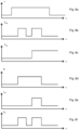
- the first filter 4a is a low-pass filter whose transmission curve is illustrated in figure 3c
- the first wavelength range has shorter wavelengths than the second wavelength range.
- the first photodetector 1a receives only the wavelength range associated with the shorter wavelengths as illustrated with the intensity curve of the figure 3e .
- the second photodetector 1b receives both wavelength ranges as illustrated with the intensity curve of the figure 3f .
- There 3d figure represents the absorption wavelength range of the first and second photodetectors 1a and 1b.
- the first filter 4a is a high-pass filter whose transmission curve is illustrated in figure 4c
- the first wavelength range has longer wavelengths than the second wavelength range.
- the first photodetector 1a receives only the wavelength range wavelength associated with the longest wavelengths as illustrated with the intensity curve of the figure 4e .
- the second photodetector 1b receives both wavelength ranges as illustrated with the intensity curve of the figure 4f .
- There figure 4d represents the absorption wavelength range of the first and second photodetectors 1a and 1b.
- the first wavelength range may have shorter or longer wavelengths than the second wavelength range depending on the characteristics of the first filter 4a. If the first filter 4a is configured to pass the shorter wavelengths then the operation is equivalent to a low-pass filter. If the first filter 4a is configured to pass the longer wavelengths then the operation is equivalent to a high-pass filter.
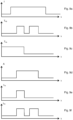
- the second filter 4b is a low-pass filter that is configured to cut off wavelengths above the upper end of the interval defined by the first and second wavelength ranges.
- a filter makes it possible to block stray radiation that corresponds to wavelengths greater than the cut-off wavelength and that can be absorbed by the photodetectors 1a and 1b ( figure 5d ).
- the first filter 4a is a low-pass filter whose transmission curve is illustrated in figure 5c
- the first wavelength range has shorter wavelengths than the second wavelength range.
- the first photodetector 1a receives only the wavelength range wavelength associated with the shortest wavelengths as illustrated with the intensity curve of the figure 5e .
- the second photodetector 1b receives both wavelength ranges as illustrated with the intensity curve of the figure 5f .
- There figure 5d represents the absorption wavelength range of the first and second photodetectors 1a and 1b.
- the first filter 4a is a high-pass filter whose transmission curve is illustrated in figure 6c
- the first wavelength range has longer wavelengths than the second wavelength range.
- the first photodetector 1a receives only the wavelength range associated with the longer wavelengths as illustrated with the intensity curve of the figure 6e .
- the second photodetector 1b receives both wavelength ranges as illustrated with the intensity curve of the figure 6f .
- There figure 6d represents the absorption wavelength range of the first and second photodetectors 1a and 1b.
- the first wavelength range may have shorter or longer wavelengths than the second wavelength range depending on the characteristics of the first filter 4a. If the first filter 4a is configured to pass the shorter wavelengths then the operation is equivalent to a low-pass filter. If the first filter 4a is configured to pass the longer wavelengths then the operation is equivalent to a high-pass filter.
- the second filter 4b is a bandpass filter which is configured to cut off wavelengths below the lower end of the interval defined by the first and second wavelength ranges and to cut off wavelengths above the upper end of the interval defined by the first and second wavelength ranges.
- a filter makes it possible to block parasitic radiation which corresponds to lengths below and above the two cut-off wavelengths and which can be absorbed by the photodetectors 1a and 1b ( figure 7d ).
- the first filter 4a can be a high-pass filter, a low-pass filter or a band-pass filter.
- the first filter 4a is a high-pass filter whose transmission curve is illustrated in figure 7c
- the first wavelength range has longer wavelengths than the second wavelength range.
- the first photodetector 1a receives only the wavelength range associated with the longer wavelengths as illustrated with the intensity curve of the figure 7e .
- the second photodetector 1b receives both wavelength ranges as illustrated with the intensity curve of the figure 7f .
- There figure 7d represents the absorption wavelength range of the first and second photodetectors 1a and 1b.
- the first filter 4a is a low-pass filter (not shown)
- the first wavelength range has shorter wavelengths than the second wavelength range.
- the first photodetector 1a receives only the wavelength range associated with the shorter wavelengths.
- the second photodetector 1b receives both wavelength ranges.
- the first wavelength range may have shorter or longer wavelengths than the second wavelength range depending on the characteristics of the first filter 4a. If the first filter 4a is configured to pass the shorter wavelengths then the operation is equivalent to a low-pass filter. If the first filter 4a is configured to pass the longer wavelengths then the operation is equivalent to a high-pass filter.
- the second filter 4b is a bi-lobe filter whose transmission curve is illustrated in figure 8b
- the bi-lobe filter is associated with a first high-pass filter 4a whose transmission curve is illustrated in figure 8c .
- the first photodetector 1a receives only the wavelength range associated with the longest wavelengths as illustrated with the intensity curve of the figure 8e .
- the second photodetector 1b receives both wavelength ranges as illustrated with the intensity curve of the figure 8f .
- There figure 8d represents the absorption wavelength range of the first and second photodetectors 1a and 1b.
- the first filter 4a may be replaced by a band-pass filter or by a low-pass filter which is illustrated by the Figures 9a to 9f .
- the transmission curve of the low-pass filter is shown in figure 9c .
- the first photodetector 1a receives only the wavelength range associated with the shortest wavelengths as illustrated with the intensity curve of the figure 9e .
- the second photodetector 1b receives both wavelength ranges as illustrated with the intensity curve of the figure 9f .
- There figure 9d represents the wavelength range absorbed by the first and second photodetectors 1a and 1b.
- the second photodetector 1b is covered by a third filter 4c.
- the third filter 4c is configured to pass the second wavelength range and block the first wavelength range.
- the third filter 4c may be an interference filter or an absorption filter.
- the third filter 4c can be a low-pass filter or a high-pass filter whose cutoff wavelength lies between the first wavelength range and the second wavelength range. If the first filter is a low-pass filter, the second filter is a high-pass filter and vice versa.
- the third filter 4c is a band-pass filter which passes the second wavelength range and blocks the first wavelength range.
- This embodiment is less advantageous than the previous one because a band-pass filter is thicker than a low-pass or high-pass filter.
- the third filter 4c is a filter deposited directly on the second photodetector 1b, that is to say on a part of the focal plane array.
- the third filter 4c is not deposited on the first photodetector 1a so the third filter 4c only covers the second photodetector 1b and it leaves the first photodetector 1a uncovered.
- the third filter 4c is in physical contact with the second photodetector.
- the third filter 4c makes it possible to limit the crosstalk between the first photodetector 1a and the adjacent second photodetector 1b.
- the second photodetector 1b receives only a part of the incident radiation.
- the second photodetector 1b receives the second wavelength range and it does not receive the first wavelength range.
- Each photodetector provides information representative of the observed wavelength range.
- the processing circuit can be simplified because it is no longer necessary to compare the signals from the two photodetectors.
- the emission curve of the observed scene extends beyond the first and second wavelength ranges.
- the detection device can be simply realized in the following manner.
- the first photodetector 1a and the second photodetector 1b are formed on a semiconductor substrate. Since the two photodetectors 1a and 1b are sensitive to the same wavelength ranges, it is advantageous to realize the two photodetectors simultaneously and with the same semiconductor materials. In a preferred embodiment, the photodetectors 1a and 1b are identical.
- the two photodetectors are offset along an axis parallel to the plane of the substrate surface and they are in the same plane which is parallel to the plane of the substrate surface.
- a first filter 4a is formed on the first photodetector 1a so as to cover the first photodetector 1a and to leave the second photodetector 1b uncovered.
- the first filter 4a is formed on the first photodetector 1a and on the second photodetector 1b. The first filter 4a is then removed above the second photodetector 1b.
- the second photodetector 1b is protected by a sacrificial layer.
- the first filter 4a is formed on the first photodetector 1a and on the sacrificial layer.
- the sacrificial layer is removed so as to release the second photodetector 1b which is devoid of a first filter.
- the second filter 4b is associated, for example brought into contact, with the substrate containing the first photodetector 1a and the second photodetector 1b.
- the second filter 4b is not formed by deposition on the substrate, it was formed independently and it is reported subsequently.
- the first filter 4a can be formed before or after the third filter 4c. It is also possible to provide that the first filter 4a and the third filter 4c are formed partly simultaneously by sharing some layers.
- the third filter 4c is produced before installing the second filter 4b. the third filter 4c is arranged at a distance from the second filter 4b.
- first and second photodetectors 1a and 1b in a closed enclosure that is advantageously sealed.
- This closed enclosure includes an orifice configured to allow radiation to pass from the radiation source to the first and second photodetectors 1a and 1b.
- the second filter 4b in this orifice so as to allow the first and second wavelength ranges to pass and to block a portion of the unnecessary radiation.
- the orifice is advantageously a window 6 made of transparent material covered by the second filter 4b.
- the second filter 4b may be located inside the closed enclosure ( figure 1 ) or outside the closed enclosure ( figure 2 ). The entire surface of the window is advantageously covered by the second filter 4b in order to leave only the useful signal in all areas of the window.
- the detection device is a cooled detection device, i.e. a device that is configured to operate at a temperature below 300K, preferably between 40K and 300K and preferably below 200K.
- the detection device may also be uncooled.
- the detection device is advantageously coupled to a cooling system 7 which allows it to be cooled to its operating temperature.
- the photodetectors of the detection device can be made of II-VI material, for example HgCdTe or of III-V material, for example InGaAs, InSb, InAsSb.
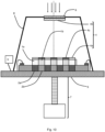
- the photodetectors 1a and 1b are advantageously surrounded by a cold screen 8 which is configured to block the incident radiation with the exception of the window 6 for the passage of the incident radiation. It appears particularly advantageous to place the second filter 4b on this window 6 for the passage of the incident radiation.
- the areas covered by the first filter 4a and the areas left uncovered by the first filter 4a advantageously define an alternation between the first photodetectors 1a and the second photodetectors 1b.
- This alternation between the first and second photodetectors can result in the creation of a checkerboard or an alternation of bands represented by rows or columns of photodetectors.
- the pressure inside the cold screen 8 is less than or equal to the pressure outside the cold screen 8. It is advantageous to provide that the pressure inside the cold screen 8 is lower than atmospheric pressure, for example lower than 1013hPa.
- the pressure inside the cold shield is less than 10 -4 Pa.
Landscapes
- Photometry And Measurement Of Optical Pulse Characteristics (AREA)
- Physics & Mathematics (AREA)
- Spectroscopy & Molecular Physics (AREA)
- Color Television Image Signal Generators (AREA)
- Light Receiving Elements (AREA)
- Spectrometry And Color Measurement (AREA)
- Solid State Image Pick-Up Elements (AREA)
- Investigating Or Analysing Materials By Optical Means (AREA)
- Measurement Of Resistance Or Impedance (AREA)
- Measurement And Recording Of Electrical Phenomena And Electrical Characteristics Of The Living Body (AREA)
Description
L'invention est relative à un dispositif de détection multispectrale.The invention relates to a multispectral detection device.
L'invention est également relative à un procédé de fabrication d'un dispositif de détection multispectrale.The invention also relates to a method of manufacturing a multispectral detection device.
Dans le domaine des dispositifs de détection, afin de capter un maximum d'information sur une scène en cours d'observation, il est avantageux d'utiliser plusieurs bandes spectrales différentes.In the field of detection devices, in order to capture a maximum of information on a scene being observed, it is advantageous to use several different spectral bands.
Plusieurs détecteurs sont utilisés et ils sont associés à des bandes spectrales différentes. De cette manière, chaque détecteur vient capter une information spécifique de la scène observée ce qui permet de faciliter l'analyse en croisant les différentes données.Several detectors are used and they are associated with different spectral bands. In this way, each detector captures specific information from the observed scene, which facilitates the analysis by crossing the different data.
Une manière simple de réaliser un dispositif de détection est d'associer plusieurs photodétecteurs différents qui sont configurés pour détecter une bande spectrale spécifique. Chaque photodétecteur est associé à un circuit de lecture qui va stocker les charges électriques représentatives de l'information reçue.A simple way to realize a detection device is to associate several different photodetectors that are configured to detect a specific spectral band. Each photodetector is associated with a reading circuit that will store the electrical charges representative of the information received.
L'information électrique générée est ensuite envoyée à un circuit de traitement qui analyse les différentes données pour fournir une information exploitable par l'utilisateur.The electrical information generated is then sent to a processing circuit which analyzes the different data to provide information that can be used by the user.
De manière classique, le dispositif de détection comporte des premiers photodétecteurs qui sont réalisés selon une première architecture et avec des premiers matériaux semi-conducteurs de manière à détecter un rayonnement dans une première bande spectrale. Le dispositif de détection comporte également des deuxièmes photodétecteurs qui sont réalisés dans une deuxième architecture qui peut être différente de la première architecture. Les deuxièmes photodétecteurs sont réalisés dans des deuxièmes matériaux semi-conducteurs différents des premiers matériaux semi-conducteurs de manière à détecter le rayonnement dans la deuxième bande spectrale.Conventionally, the detection device comprises first photodetectors which are produced according to a first architecture and with first semiconductor materials so as to detect radiation in a first spectral band. The detection device also comprises second photodetectors which are produced in a second architecture which may be different from the first architecture. The second photodetectors are produced in second semiconductor materials different from the first semiconductor materials so as to detect the radiation in the second spectral band.
Un tel mode de réalisation est compliqué à mettre en œuvre car il nécessite de réaliser deux empilements différents avec des matériaux semi-conducteurs différents pour former deux types de photodétecteurs différents.Such an embodiment is complicated to implement because it requires making two different stacks with different semiconductor materials to form two different types of photodetectors.
En alternative, il est proposé de réaliser des premier et deuxième photodétecteurs qui sont tous les deux sensibles à la première bande spectrale et à la deuxième bande spectrale.Alternatively, it is proposed to provide first and second photodetectors which are both sensitive to the first spectral band and to the second spectral band.
Afin de spécialiser les photodétecteurs sur la première bande spectrale ou sur la deuxième spectrale, des filtres sont associés à chacun des photodétecteurs. Des premiers filtres sont disposés uniquement au-dessus des premiers photodétecteurs de manière à ne laisser passer que la première bande spectrale. Des deuxièmes filtres sont disposés uniquement au-dessus des deuxièmes photodétecteurs de manière à ne laisser passer que la deuxième bande spectrale. Un tel enseignement est décrit dans le document
Cependant, il apparaît qu'un tel mode de réalisation est également très compliqué à mettre en œuvre car il nécessite la réalisation d'un premier filtre au-dessus des premiers photodétecteurs et la réalisation d'un deuxième filtre au-dessus des deuxièmes photodétecteurs. Il faut donc réaliser les deux filtres sur le réseau de photodétecteurs.However, it appears that such an embodiment is also very complicated to implement because it requires the production of a first filter above the first photodetectors and the production of a second filter above the second photodetectors. It is therefore necessary to realize the two filters on the photodetector network.
Un enseignement sensiblement équivalent est décrit dans le document
Un mode de réalisation alternatif est décrit dans le document
Le premier filtre permet un passage du rayonnement infrarouge jusqu'à la longueur d'onde de 9 microns. Le photodétecteur est configuré pour détecter un rayonnement compris entre 7 et 9 microns. Le pixel va donc délivrer un signal représentatif du rayonnement compris entre 7 et 9 microns.The first filter allows infrared radiation to pass through up to a wavelength of 9 microns. The photodetector is configured to detect radiation between 7 and 9 microns. The pixel will therefore deliver a signal representative of radiation between 7 and 9 microns.
Le deuxième filtre autorise le passage du rayonnement infrarouge jusqu'à la longueur d'onde de 10 microns. Le photodétecteur associé est configuré pour détecter un rayonnement compris entre 7 et 9 microns et un rayonnement compris entre 9 et 10 microns. Le deuxième pixel va donc délivrer un signal représentatif du rayonnement compris entre 7 et 10 microns.The second filter allows the passage of infrared radiation up to a wavelength of 10 microns. The associated photodetector is configured to detect radiation between 7 and 9 microns and radiation between 9 and 10 microns. The second pixel will therefore deliver a signal representative of radiation between 7 and 10 microns.
Une autre variante de réalisation est décrite dans le document
Tous les photodétecteurs sont recouverts par un filtre interférentiel bi-bande qui est configuré pour laisser passer les rayonnements d'une première bande spectrale et d'une deuxième bande spectrale.All photodetectors are covered by a dual-band interference filter which is configured to pass radiation from a first spectral band and a second spectral band.
Une partie de ces photodétecteurs est recouverte par un filtre passe-bas afin de ne recevoir que le rayonnement de la première bande spectrale. L'autre partie de ces photodétecteurs est recouverte par un filtre passe-haut afin de ne recevoir que le rayonnement de la deuxième bande spectrale.A part of these photodetectors is covered by a low-pass filter in order to receive only the radiation of the first spectral band. The other part of these photodetectors is covered by a high-pass filter in order to receive only the radiation of the second spectral band.
Il apparaît que cette solution est particulièrement complexe à mettre en œuvre et onéreuse.It appears that this solution is particularly complex to implement and expensive.
Le document
Le document
Le document
L'invention a comme objet de fournir un dispositif de détection multispectral qui peut être réalisé plus facilement et qui peut être plus compact.The object of the invention is to provide a multispectral detection device which can be produced more easily and which can be more compact.
On tend à atteindre ce résultat au moyen d'un dispositif selon la revendication 1, donc au moyen d'un dispositif de détection multispectrale qui comporte, entre autre :
- un premier photodétecteur et un deuxième photodétecteur sensibles chacun à une première gamme de longueur d'onde et à une deuxième gamme de longueur d'onde différente de la première gamme de longueur d'onde, le premier photodétecteur délivrant un premier signal représentatif du rayonnement reçu et le deuxième photodétecteur délivrant un deuxième signal représentatif du rayonnement reçu,
- un premier filtre configuré pour laisser passer la première gamme de longueur d'onde et pour bloquer la deuxième gamme de longueur d'onde, le premier filtre recouvrant le premier photodétecteur et laissant découvert le deuxième photodétecteur, le premier filtre étant en contact avec le premier photodétecteur de manière à bloquer le passage de la deuxième gamme de longueur d'onde dans le premier photodétecteur,
- un deuxième filtre disposé à distance du premier et du deuxième photodétecteurs et à distance du premier filtre, le deuxième filtre étant configuré pour laisser passer la première gamme de longueur d'onde et la deuxième gamme de longueur d'onde, le deuxième filtre étant configuré pour bloquer une longueur d'onde supérieure à la plus longue des longueurs d'onde parmi les première et deuxième gammes de longueur d'onde et/ou pour bloquer une longueur d'onde inférieure à la plus courte des longueurs d'onde parmi les première et deuxième gammes de longueur d'onde.
- a first photodetector and a second photodetector each sensitive to a first wavelength range and to a second wavelength range different from the first wavelength range, the first photodetector delivering a first signal representative of the radiation received and the second photodetector delivering a second signal representative of the radiation received,
- a first filter configured to pass the first wavelength range and to block the second wavelength range, the first filter covering the first photodetector and leaving the second photodetector uncovered, the first filter being in contact with the first photodetector so as to block the passage of the second wavelength range into the first photodetector,
- a second filter arranged spaced from the first and second photodetectors and spaced from the first filter, the second filter being configured to pass the first wavelength range and the second wavelength range, the second filter being configured to block a wavelength greater than the longest of the wavelengths among the first and second wavelength ranges and/or to block a wavelength less than the shortest of the wavelengths among the first and second wavelength ranges.
Dans un développement, le deuxième photodétecteur est dépourvu de filtre configuré pour bloquer la première gamme de longueur d'onde de manière à recevoir la première gamme de longueur d'onde et la deuxième gamme de longueur d'onde, le dispositif de détection comportant un circuit de traitement configuré pour recevoir des signaux électriques en provenance des premier et deuxième photodétecteurs et fournir une information relative au rayonnement de la deuxième gamme de longueur d'onde par comparaison du premier signal avec le deuxième signal.In one development, the second photodetector is devoid of a filter configured to block the first wavelength range so as to receive the first wavelength range and the second wavelength range, the detection device comprising a processing circuit configured to receive electrical signals from the first and second photodetectors and provide information relating to the radiation of the second wavelength range by comparing the first signal with the second signal.
En alternative, le deuxième photodétecteur est recouvert par un troisième filtre configuré pour bloquer la première gamme de longueur d'onde et laisser passer la deuxième gamme de longueur d'onde.Alternatively, the second photodetector is covered by a third filter configured to block the first wavelength range and pass the second wavelength range.
Dans un mode de réalisation avantageux, le deuxième filtre est choisi parmi les filtres passe-bas, passe-haut, passe-bande et bi-bande.In an advantageous embodiment, the second filter is selected from low-pass, high-pass, band-pass and dual-band filters.
Préférentiellement, le premier filtre est un filtre passe-bas, passe-haut ou passe-bande coupant la deuxième gamme de longueur d'onde.Preferably, the first filter is a low-pass, high-pass or band-pass filter cutting the second wavelength range.
Il est intéressant de prévoir que le deuxième filtre est disposé à distance du premier filtre et du deuxième photodétecteur par une couche de gaz ou du vide. It is interesting to provide that the second filter is arranged at a distance from the first filter and the second photodetector by a layer of gas or vacuum.
Dans un mode de réalisation, le dispositif de détection comporte un écran froid configuré pour focaliser le rayonnement incident au moyen d'un orifice de passage du rayonnement et le deuxième filtre est disposé dans ledit orifice.In one embodiment, the detection device comprises a cold shield configured to focus incident radiation using an orifice radiation passage and the second filter is arranged in said orifice.
Préférentiellement, l'écran froid définit une enceinte fermée contenant les premier et deuxième photodétecteurs et le deuxième filtre est disposé dans l'enceinte fermée.Preferably, the cold screen defines a closed enclosure containing the first and second photodetectors and the second filter is arranged in the closed enclosure.
En alternative, l'écran froid définit une enceinte fermée contenant les premier et deuxième photodétecteurs et le deuxième filtre est disposé hors de l'enceinte fermée.Alternatively, the cold shield defines a closed enclosure containing the first and second photodetectors and the second filter is disposed outside the closed enclosure.
L'invention a également comme objet de réaliser un procédé de fabrication d'un dispositif de détection multispectrale qui soit plus simple.The invention also aims to provide a simpler method of manufacturing a multispectral detection device.
On tend à atteindre ce résultat au moyen d'un procédé de fabrication selon la revendication 10, donc au moyen d'un procédé de fabrication d'un dispositif de détection multispectrale qui comporte, entre autre, les étapes suivantes :
- prévoir un substrat comportant des premier et deuxième photodétecteurs sensibles chacun à une première gamme de longueur d'onde et à une deuxième gamme de longueur d'onde différente de la première gamme de longueur d'onde, le premier photodétecteur délivrant un premier signal représentatif du rayonnement reçu et le deuxième photodétecteur délivrant un deuxième signal représentatif du rayonnement reçu,
- former un premier filtre configuré pour laisser passer la première gamme de longueur d'onde et pour bloquer la deuxième gamme de longueur d'onde, le premier filtre recouvrant le premier photodétecteur et laissant découvert le deuxième photodétecteur, le premier filtre étant en contact avec le premier photodétecteur de manière à bloquer le passage de la deuxième gamme de longueur d'onde dans le premier photodétecteur,
- former un deuxième filtre disposé à distance du premier et du deuxième photodétecteurs et à distance du premier filtre, le deuxième filtre étant configuré pour laisser passer la première gamme de longueur d'onde et la deuxième gamme de longueur d'onde, le deuxième filtre étant configuré pour bloquer une longueur d'onde supérieure à la plus longue des longueurs d'onde parmi les première et deuxième gammes de longueur d'onde et/ou pour bloquer une longueur d'onde inférieure à la plus courte des longueur d'onde parmi les première et deuxième gammes de longueur d'onde.
- providing a substrate comprising first and second photodetectors each sensitive to a first wavelength range and to a second wavelength range different from the first wavelength range, the first photodetector delivering a first signal representative of the radiation received and the second photodetector delivering a second signal representative of the radiation received,
- forming a first filter configured to pass the first wavelength range and to block the second wavelength range, the first filter covering the first photodetector and leaving the second photodetector uncovered, the first filter being in contact with the first photodetector so as to block the passage of the second wavelength range into the first photodetector,
- forming a second filter disposed spaced from the first and second photodetectors and spaced from the first filter, the second filter being configured to pass the first wavelength range and the second wavelength range, the second filter being configured to block a wavelength greater than the longest of the wavelengths among the first and second wavelength ranges and/or to block a wavelength less than the shortest of the wavelengths among the first and second wavelength ranges.
Dans un développement particulier, le procédé comporte, avant de former le deuxième filtre :
- former un troisième filtre configuré pour laisser passer la deuxième gamme de longueur d'onde et pour bloquer la première gamme de longueur d'onde, le troisième filtre recouvrant le deuxième photodétecteur et laissant découvert le premier photodétecteur, le troisième filtre étant en contact avec le deuxième photodétecteur de manière à bloquer le passage de la première gamme de longueur d'onde dans le deuxième photodétecteur.
- forming a third filter configured to pass the second wavelength range and to block the first wavelength range, the third filter covering the second photodetector and leaving the first photodetector uncovered, the third filter being in contact with the second photodetector so as to block the passage of the first wavelength range into the second photodetector.
D'autres avantages et caractéristiques ressortiront plus clairement de la description qui va suivre de modes particuliers de réalisation de l'invention donnés à titre d'exemples non limitatifs et représentés aux dessins annexés, dans lesquels :
- les
figures 1 et2 représentent, de manière schématique, deux modes de réalisation alternatifs d'un dispositif de détection muni de deux photodétecteurs et d'un filtre sur l'écran froid, - les
figures 3a-3f représentent, de manière schématique, des courbes d'intensité, de transmittance et d'absorbance des différents constituants du dispositif de détection selon un premier mode de réalisation, - les
figures 4a-4f représentent, de manière schématique, des courbes d'intensité, de transmittance et d'absorbance des différents constituants du dispositif de détection selon un deuxième mode de réalisation, - les
figures 5a-5f représentent, de manière schématique, des courbes d'intensité, de transmittance et d'absorbance des différents constituants du dispositif de détection selon un troisième mode de réalisation, - les
figures 6a-6f représentent, de manière schématique, des courbes d'intensité, de transmittance et d'absorbance des différents constituants du dispositif de détection selon un quatrième mode de réalisation, - les
figures 7a-7f représentent, de manière schématique, des courbes d'intensité, de transmittance et d'absorbance des différents constituants du dispositif de détection selon un cinquième mode de réalisation, - les
figures 8a-8f représentent, de manière schématique, des courbes d'intensité, de transmittance et d'absorbance des différents constituants du dispositif de détection selon un sixième mode de réalisation, - les
figures 9a-9f représentent, de manière schématique, des courbes d'intensité, de transmittance et d'absorbance des différents constituants du dispositif de détection selon un septième mode de réalisation, - la
figure 10 représente, de manière schématique, un autre mode de réalisation d'un dispositif de détection muni de deux photodétecteurs et d'un filtre sur l'écran froid.
- THE
figures 1 And2 schematically represent two alternative embodiments of a detection device provided with two photodetectors and a filter on the cold screen, - THE
Figures 3a-3f schematically represent intensity, transmittance and absorbance curves of the different constituents of the detection device according to a first embodiment, - THE
Figures 4a-4f schematically represent intensity, transmittance and absorbance curves of the different constituents of the detection device according to a second embodiment, - THE
Figures 5a-5f schematically represent intensity, transmittance and absorbance curves of the different constituents of the detection device according to a third embodiment, - THE
Figures 6a-6f schematically represent intensity, transmittance and absorbance curves of the different constituents of the detection device according to a fourth embodiment, - THE
Figures 7a-7f schematically represent intensity, transmittance and absorbance curves of the different constituents of the detection device according to a fifth embodiment, - THE
Figures 8a-8f schematically represent intensity, transmittance and absorbance curves of the different constituents of the detection device according to a sixth embodiment, - THE
Figures 9a-9f schematically represent intensity, transmittance and absorbance curves of the different constituents of the detection device according to a seventh embodiment, - there
figure 10 schematically represents another embodiment of a detection device provided with two photodetectors and a filter on the cold screen.
Les
Dans un mode de réalisation particulier, le premier photodétecteur 1a et le deuxième photodétecteur 1b comportent un seul film semi-conducteur qui est configuré pour absorber la première gamme de longueur d'onde et la deuxième gamme de longueur d'onde. Ce mode de réalisation est particulièrement avantageux car il est très compact.In a particular embodiment, the
Dans une variante de réalisation, le premier photodétecteur 1a et le deuxième photodétecteur 1b comportent chacun des premier et deuxième films semi-conducteurs distincts qui sont respectivement configurés pour capter la première gamme de longueur d'onde et la deuxième gamme de longueur d'onde.In an alternative embodiment, the
Ces deux modes de réalisation sont avantageux car les deux photodétecteurs peuvent être réalisés simultanément ce qui facilite le procédé de fabrication et la densité d'intégration.These two embodiments are advantageous because the two photodetectors can be produced simultaneously, which facilitates the manufacturing process and the integration density.
Dans un mode de réalisation avantageux, le dispositif de détection multispectrale comporte une pluralité de premiers photodétecteurs et une pluralité de deuxièmes photodétecteurs. De manière avantageuse, les premiers photodétecteurs et les deuxièmes photodétecteurs forment un réseau. Il est particulièrement avantageux de prévoir que les premiers photodétecteurs et les deuxièmes photodétecteurs sont uniformément répartis sur la surface de détection.In an advantageous embodiment, the multispectral detection device comprises a plurality of first photodetectors and a plurality of second photodetectors. Advantageously, the first photodetectors and the second photodetectors form an array. It is particularly advantageous to provide that the first photodetectors and the second photodetectors are uniformly distributed over the detection surface.
Dans un mode de réalisation avantageux, la pluralité de premiers photodétecteurs et la pluralité de deuxièmes photodétecteurs forment un réseau plan focal, c'est-à-dire que tous les photodétecteurs sont réalisés dans un même plan.In an advantageous embodiment, the plurality of first photodetectors and the plurality of second photodetectors form a focal plane array, i.e. all the photodetectors are produced in the same plane.
De manière préférentielle, le dispositif de détection comporte autant de premiers photodétecteurs que de deuxièmes photodétecteurs. En alternative, il est également possible de prévoir que le dispositif de détection comporte un nombre de premiers photodétecteurs qui est différent du nombre de deuxièmes photodétecteurs.Preferably, the detection device comprises as many first photodetectors as second photodetectors. Alternatively, it is also possible to provide that the detection device comprises a number of first photodetectors which is different from the number of second photodetectors.
Dans un mode de réalisation particulier, la deuxième gamme de longueur d'onde est différente de la première gamme de longueur d'onde. De manière avantageuse, la deuxième gamme de longueur d'onde est dissociée de la première gamme de longueur d'onde c'est-à-dire que les gammes de longueur d'onde ne se chevauchent pas. Selon les modes de réalisation, les première et deuxième gammes de longueur d'onde ont une borne commune ou elles sont séparées par une gamme de longueur d'onde intermédiaire.In a particular embodiment, the second wavelength range is different from the first wavelength range. Advantageously, the second wavelength range is dissociated from the first wavelength range, i.e. the wavelength ranges do not overlap. According to the embodiments, the first and second wavelength ranges have a common terminal or they are separated by an intermediate wavelength range.
Le premier photodétecteur 1a et le deuxième photodétecteur 1b sont tous les deux sensibles à la première gamme de longueur d'onde et à la deuxième gamme de longueur d'onde. En d'autres termes, le premier photodétecteur 1a et le deuxième photodétecteur 1b sont en mesure de capter le rayonnement émis dans la première gamme de longueur d'onde et de fournir un signal électrique représentatif de ce rayonnement. Le premier photodétecteur 1a et le deuxième photodétecteur 1b sont également en mesure de capter le rayonnement émis dans la deuxième gamme de longueur d'onde et de fournir un signal électrique représentatif de ce rayonnement.The
Il est également possible que le premier photodétecteur 1a et le deuxième photodétecteur 1b soient en mesure de capter le rayonnement émis dans une troisième gamme de longueur d'onde qui est différente des première et deuxième gammes de longueur d'onde. Cette troisième gamme de longueur d'onde ne contient pas d'information pertinente, mais elle permet de faciliter la réalisation des photodétecteurs en choisissant des matériaux semi-conducteurs plus faciles à utiliser.It is also possible that the
Les première et deuxième gammes de longueur d'onde sont des gammes du rayonnement infrarouge. Dans un mode de réalisation particulier, la première gamme de longueur d'onde et la deuxième gamme de longueur d'onde sont choisies parmi les gammes suivantes :
- NIR : entre 0,8µm et 1,4µm
- SWIR : entre 1,4µm et 3µm,
- MWIR : entre 3µm et 8µm,
- LWIR : entre 8µm et 15µm.
- NIR: between 0.8µm and 1.4µm
- SWIR: between 1.4µm and 3µm,
- MWIR: between 3µm and 8µm,
- LWIR: between 8µm and 15µm.
Il est donc possible de configurer le dispositif de détection afin que ce dernier puisse détecter différents couples de gammes de longueur d'onde, par exemple MWIR/LWIR, MWIR/SWIR, LWIR/SWIR, NIR/SWIR, NIR/LWIR ou NIR/MWIR.It is therefore possible to configure the detection device so that it can detect different pairs of wavelength ranges, for example MWIR/LWIR, MWIR/SWIR, LWIR/SWIR, NIR/SWIR, NIR/LWIR or NIR/MWIR.
Il est encore possible de découper les différentes gammes présentées cidessus en deux sous-gammes différentes. Dans un mode de réalisation particulier, les première et deuxième gammes de longueur d'onde divisent par exemple le rayonnement MWIR en deux sous-gammes distinctes. Il peut en être de même pour les rayonnements LWIR, SWIR ou NIR.It is also possible to divide the different ranges presented above into two different sub-ranges. In a particular embodiment, the first and second wavelength ranges divide, for example, the MWIR radiation into two distinct sub-ranges. The same may apply to LWIR, SWIR or NIR radiation.
Le premier et le deuxième photodétecteurs 1a et 1b peuvent être formés par tout type de détecteur adapté, par exemple par une photodiode, un détecteur à puits quantique ou un détecteur à multipuits quantiques. D'autres types de photodétecteurs sont également possibles. Les premier et deuxième photodétecteurs 1a et 1b peuvent être réalisés dans des architectures identiques ou différentes. De manière avantageuse, le premier photodétecteur 1a est identique au deuxième photodétecteur 1b, c'est-à-dire dans les matériaux et dans l'architecture de réalisation. Il est alors beaucoup plus facile de réaliser les photodétecteurs de manière compacte.The first and
Les conditions d'alimentation des photodétecteurs 1a et 1b peuvent être différentes. Avantageusement, les conditions d'alimentation sont identiques pour tous les photodétecteurs. Les conditions d'alimentation sont fournies par un premier circuit de lecture 2a pour le premier photodétecteur 1a et par un deuxième circuit de lecture 2b pour le deuxième photodétecteur 1b.The power supply conditions of the
Les photodétecteurs 1a et 1b et les circuits de lecture 2a et 2b sont avantageusement disposé sur un support 3.The
Afin de spécialiser les premier et deuxième photodétecteurs 1a et 1b, les photodétecteurs sont associés à un système de filtrage 4 du rayonnement incident. Le système de filtrage 4 est configuré pour que le premier photodétecteur 1a reçoive un rayonnement différent du deuxième photodétecteur 1b. De cette manière, les deux photodétecteurs 1a et 1b sont en mesure de fournir deux informations différentes sur la scène observée.In order to specialize the first and
Comme indiqué plus haut, l'utilisation de photodétecteurs identiques permet de faciliter la réalisation d'un dispositif compact. Cependant, la compacité est telle qu'il devient difficile de réaliser des filtres différents et performants au-dessus du premier photodétecteur 1a et au-dessus du deuxième photodétecteur 1b.As indicated above, the use of identical photodetectors makes it easier to produce a compact device. However, the compactness is such that it becomes difficult to produce different and efficient filters above the
Afin de faciliter la réalisation d'un dispositif de détection performant, le système de filtrage 4 est un système de filtrage dissocié, c'est-à-dire qu'il comporte au moins un premier filtre 4a et un deuxième filtre 4b qui présentent des propriétés optiques différentes et qui sont disposés successivement dans le chemin optique du premier photodétecteur 1a. Le premier filtre 4a et le deuxième filtre 4b ne sont pas en contact l'un avec l'autre ce qui permet de faciliter la réalisation du système de filtrage 4. Le premier filtre 4a présente des caractéristiques optiques et préférentiellement mécaniques différentes du deuxième filtre 4b.In order to facilitate the production of a high-performance detection device, the
L'utilisation de deux filtres dissociés et consécutifs dans le chemin optique permet de réduire l'épaisseur du filtre disposé en contact avec le photodétecteur en comparaison d'un filtre équivalent qui est également en contact avec le photodétecteur.The use of two separate and consecutive filters in the optical path makes it possible to reduce the thickness of the filter placed in contact with the photodetector in comparison with an equivalent filter which is also in contact with the photodetector.
Typiquement, l'épaisseur d'un filtre est sensiblement égale à la longueur d'onde de la fréquence de coupure. Ainsi, pour un photodétecteur configuré pour absorber un rayonnement dans la gamme 3-5µm, le filtre équivalent présente une épaisseur sensiblement comprise entre 3µm et 5µm.Typically, the thickness of a filter is substantially equal to the wavelength of the cutoff frequency. Thus, for a photodetector configured to absorb radiation in the 3-5µm range, the equivalent filter has a thickness substantially between 3µm and 5µm.
Il apparaît clairement qu'une telle épaisseur pose un problème de fabrication pour les réseaux de photodétecteurs dont le pas de répétition est inférieur à 30µm. Le problème d'intégration est encore plus critique pour les réseaux de photodétecteurs dont le pas de répétition est inférieur à 20µm. Des problèmes importants de réalisation sont présents pour les réseaux de photodétecteurs dont le pas de répétition est inférieur à 15µm et notamment lorsque le filtre possède une épaisseur égale à 5µm.It is clear that such a thickness poses a manufacturing problem for photodetector arrays with a repetition pitch of less than 30 µm. The integration problem is even more critical for photodetector arrays with a repetition pitch of less than 20 µm. Significant manufacturing problems are present for photodetector arrays with a repetition pitch of less than 15 µm and in particular when the filter has a thickness of 5 µm.
Il apparaît encore que pour accroitre les performances du filtre et notamment pour accroitre sa capacité à bloquer efficacement une partie du rayonnement incident, le nombre de couches formant le filtre doit être augmenté ce qui augmente l'épaisseur du filtre. Par exemple, pour accroitre le pouvoir de réjection du filtre, c'est-à-dire sa capacité à bloquer le rayonnement incident de 10% par rapport à un filtre de référence, l'augmentation de l'épaisseur est de l'ordre de 2µm.It also appears that to increase the performance of the filter and in particular to increase its capacity to effectively block part of the incident radiation, the number of layers forming the filter must be increased, which increases the thickness of the filter. For example, to increase the rejection power of the filter, i.e. its capacity to block the incident radiation by 10% compared to a reference filter, the increase in thickness is of the order of 2 µm.
Il apparaît également que pour les dispositifs de détection qui fonctionnent à basse température, typiquement en dessous de 0°C, le filtre introduit des contraintes thermomécaniques importantes dans le photodétecteur ce qui dégrade les performances du dispositif de détection. Les contraintes thermomécaniques augmentent lorsque l'épaisseur augmente.It also appears that for detection devices operating at low temperatures, typically below 0°C, the filter introduces significant thermomechanical stresses into the photodetector which degrades the performance of the detection device. The thermomechanical stresses increase as the thickness increases.
Le système de filtrage 4 comporte un premier filtre 4a qui est configuré pour laisser passer la première gamme de longueur d'onde et pour bloquer la deuxième gamme de longueur d'onde. Le premier filtre 4a peut être un filtre interférentiel ou un filtre à absorption.The
Selon les modes de réalisation, la première gamme de longueur d'onde peut présenter des longueurs d'onde plus longues ou plus courtes que la deuxième gamme de longueur d'onde. Le premier filtre 4a peut donc être un filtre passe-bas ou un filtre passe-haut dont la longueur d'onde de coupure se trouve entre la première gamme de longueur d'onde et la deuxième gamme de longueur d'onde. Ce mode de réalisation est particulièrement avantageux car les filtres passe-bas et passe-haut sont faciles à réaliser ce qui simplifie leur intégration à la surface des photodétecteurs. Ils sont généralement moins épais que les autres filtres.According to the embodiments, the first wavelength range may have longer or shorter wavelengths than the second wavelength range. The
En alternative, il est également possible de prévoir que le premier filtre 4a est un filtre passe-bande qui laisse passer la première gamme de longueur d'onde et qui bloque la deuxième gamme de longueur d'onde. Ce mode de réalisation est légèrement moins avantageux que le précédent car un filtre passe-bande est généralement plus épais qu'un filtre passe-bas ou passe-haut.Alternatively, it is also possible to provide that the
Le premier filtre 4a est un filtre qui est déposé directement sur le premier photodétecteur 1a, c'est-à-dire sur une partie du réseau plan focal. Le premier filtre 4a n'est pas déposé sur le deuxième photodétecteur 1b ainsi le premier filtre 4a vient recouvrir le premier photodétecteur 1a et il laisse découvert le deuxième photodétecteur 1b. Le premier filtre 4a est en contact physique avec le premier photodétecteur 1a. Le premier filtre 4a permet de limiter la diaphonie (ou crosstalk en langue anglaise) entre le premier photodétecteur 1a et le deuxième photodétecteur adjacent 1b.The
Au moyen de cette configuration particulière, le premier photodétecteur 1a ne reçoit qu'une partie du rayonnement incident. Le premier photodétecteur 1a reçoit la première gamme longueur d'onde et il ne reçoit pas la deuxième gamme longueur d'onde.By means of this particular configuration, the
Afin d'éliminer efficacement les rayonnements parasites, le système de filtrage 4 comporte également un deuxième filtre 4b. Le deuxième filtre 4b est utilisé pour bloquer une partie du rayonnement incident avant d'être capté par les premier et deuxième photodétecteurs 1a et 1b. De manière plus précise, le deuxième filtre 4b est utilisé pour bloquer une partie du rayonnement incident avant de frapper le plan focal et notamment le premier filtre 4a qui va bloquer une autre partie du rayonnement incident.In order to effectively eliminate the parasitic radiation, the
Le deuxième filtre 4b est disposé à distance du premier photodétecteur 1a et du deuxième photodétecteur 1b, c'est-à-dire que le deuxième filtre 4b n'est pas en contact direct avec le premier photodétecteur 1a, ni avec le deuxième photodétecteur 1b.The
Le deuxième filtre 4b est déposé sur un deuxième substrat qui est différent du premier substrat supportant les premier et deuxième photodétecteurs ou sur lequel sont formés les premier et deuxième photodétecteurs.The
Selon les modes de réalisation, le deuxième filtre 4b peut être un filtre interférentiel ou un filtre à absorption.Depending on the embodiments, the
Le premier filtre 4a et le deuxième filtre 4b travaillent en association pour filtrer le rayonnement reçu par le premier photodétecteur 1a.The
En séparant le premier filtre 4a et le deuxième filtre 4b, il est possible d'obtenir un filtre global capable de ne laisser passer que le rayonnement pertinent en direction du premier photodétecteur tout en limitant l'épaisseur du premier filtre 4a formé directement sur le premier photodétecteur. De cette manière, il est possible de former des premiers filtres plus compacts.By separating the
Le deuxième filtre 4b est séparé des photodétecteurs 1a et 1b et du premier filtre 4a par une couche de gaz ou de vide. De cette manière, les contraintes thermomécaniques liées au deuxième filtre 4b sont fortement réduites voire annulées. Il est alors plus facile de former le premier filtre 4a et le deuxième filtre 4b. L'épaisseur du premier filtre peut être réduite ce qui diminue les contraintes thermomécaniques.The
Dans un mode de réalisation particulier, le deuxième filtre 4b est avantageusement reporté sur le substrat contenant le premier photodétecteur 1a et le deuxième photodétecteur 1b. Le deuxième filtre 4b peut alors être formé séparément du premier filtre 4a et le procédé de réalisation du deuxième filtre 4b n'interfère pas avec le premier filtre 4a, ni avec les photodétecteurs 1a et 1b.In a particular embodiment, the
Dans une variante de réalisation, le deuxième filtre 4b est avantageusement reporté sur le support 3 qui est configuré pour supporter le substrat contenant le premier photodétecteur 1a et le deuxième photodétecteur 1b. Là encore, le deuxième filtre 4b peut alors être formé séparément du premier filtre 4a et le procédé de réalisation du deuxième filtre 4b n'interfère pas avec le premier filtre 4a, ni avec les photodétecteurs 1a et 1b.In an alternative embodiment, the
Le deuxième filtre 4b étant disposé à distance du premier filtre 4a et des photodétecteurs 1a et 1b. Le deuxième filtre 4b est un filtre commun au premier photodétecteur 1a et au deuxième photodétecteur 1b. De cette manière, le deuxième filtre 4b n'est pas lié à une contrainte d'alignement par rapport au premier filtre 4a, ni au deuxième photodétecteur 1b. Le deuxième filtre 4b se trouve entre la source de rayonnement et le premier filtre 4a ainsi que entre la source de rayonnement et le deuxième photodétecteur 1b. Le deuxième filtre 4b étant disposé à distance du premier filtre 4a et des photodétecteurs, les contraintes de fabrications et d'intégration sont réduites en comparaison des dispositifs de l'art antérieur.The
Le deuxième filtre 4b est configuré pour laisser passer la première gamme de longueur d'onde et la deuxième gamme de longueur d'onde. Le deuxième filtre 4b est avantageusement configuré pour bloquer la troisième gamme de longueur d'onde qui est différente des première et deuxième gammes de longueur d'onde.The
De manière avantageuse, le deuxième filtre 4b est un filtre coupe-bande. Il est également possible de réaliser un filtre passe-bas ou passe-haut ou bi-lobe.Advantageously, the
Selon les modes de réalisation, de façon non exhaustive, le deuxième filtre 4b peut être configuré pour bloquer les longueurs d'onde à l'extérieur des gammes suivantes :
- 0,8µm - 3µm, pour capter les rayonnements NIR et SWIR,
- 1,4µm - 8µm, pour capter les rayonnements SWIR et MWIR,
- 3µm - 15µm, pour capter les rayonnements MWIR et LWIR,
- 0,8µm - 1,4µm, pour capter le rayonnement NIR,
- 1,4µm - 3µm, pour capter le rayonnement SWIR,
- 3µm - 8µm, pour capter le rayonnement MWIR,
- 8µm - 15µm, pour capter le rayonnement LWIR,
- 0.8µm - 3µm, to capture NIR and SWIR radiation,
- 1.4µm - 8µm, to capture SWIR and MWIR radiation,
- 3µm - 15µm, to capture MWIR and LWIR radiation,
- 0.8µm - 1.4µm, to capture NIR radiation,
- 1.4µm - 3µm, to capture SWIR radiation,
- 3µm - 8µm, to capture MWIR radiation,
- 8µm - 15µm, to capture LWIR radiation,
De cette manière, le système de filtrage 4 empêche certaines longueurs d'onde d'atteindre les premier et deuxième photodétecteurs 1a/1b et de polluer les signaux utiles reçus.In this way, the
Dans un mode de réalisation particulier, le deuxième photodétecteur 1b est dépourvu de filtre disposé en contact direct avec sa surface. Dans cette configuration, le deuxième photodétecteur 1b reçoit la première longueur d'onde et la deuxième longueur d'onde car il n'est pas associé au premier filtre 4a. Ce mode de réalisation est particulièrement avantageux car seul le premier photodétecteur 1a est recouvert d'un premier filtre 4a ce qui facilite la réalisation du dispositif de détection avec des photodétecteurs de faibles dimensions.In a particular embodiment, the
Le premier photodétecteur 1a émet un signal électrique qui est représentatif du rayonnement reçu. Le signal électrique en provenance du premier photodétecteur 1a est représentatif du rayonnement dans la première gamme de longueur d'onde uniquement.The
Le deuxième photodétecteur 1b émet également un signal électrique qui est représentatif du rayonnement reçu. Le signal électrique en provenance du deuxième photodétecteur 1b est représentatif du rayonnement dans la première gamme de longueur d'onde et dans la deuxième gamme de longueurs d'onde.The
Afin d'obtenir un signal représentatif du rayonnement dans la deuxième gamme de longueur d'onde, il est avantageux de comparer le signal électrique en provenance du premier photodétecteur 1a avec le signal électrique du deuxième photodétecteur 1b.In order to obtain a signal representative of the radiation in the second wavelength range, it is advantageous to compare the electrical signal from the
Les différences d'informations entre les deux signaux sont représentatives du rayonnement dans la deuxième gamme de longueur d'onde.The differences in information between the two signals are representative of radiation in the second wavelength range.
De manière avantageuse, le premier photodétecteur 1a est connecté à un circuit de lecture/traitement 5 qui reçoit le premier signal électrique. Le deuxième photodétecteur 1b est également connecté au circuit de lecture/traitement 5 qui reçoit le deuxième signal électrique. Le circuit de lecture/traitement 5 est configuré pour comparer le premier signal électrique par rapport au deuxième signal électrique et pour fournir un troisième signal représentatif du rayonnement reçu par le deuxième photodétecteur 1b dans la deuxième gamme de longueur d'onde. Dans un mode de réalisation, le circuit de lecture/traitement peut être réalisé dans le substrat 3. Il est encore possible de dissocier les fonctions lecture et traitement et de réaliser la fonction de lecture dans le support 3. La fonction traitement est alors réalisée à part.Advantageously, the
Il est avantageux d'utiliser un deuxième filtre 4b qui est un filtre passe-haut ou un filtre passe-bas. Le deuxième filtre 4b est alors configuré pour laisser passer la première gamme de longueur d'onde et la deuxième gamme de longueur d'onde et pour bloquer une longueur d'onde supérieure à la plus grande des longueurs d'onde parmi les première et deuxième gammes de longueur d'onde ou pour bloquer la longueur d'onde inférieure à la plus petite des longueurs d'onde parmi les première et deuxième gammes de longueur d'onde.It is advantageous to use a
Il est également avantageux d'utiliser un deuxième filtre 4b dont la longueur d'onde de coupure correspond à une extrémité de l'ensemble formé par la première et la deuxième gammes de longueur d'onde. De cette manière, une partie des aléas de fabrication des photodétecteurs est éliminée.It is also advantageous to use a
Il est particulièrement avantageux de prévoir l'utilisation d'un deuxième filtre 4b qui est un filtre passe-bande dont la longueur d'onde de coupure inférieure et la longueur d'onde de coupure supérieure correspondent aux extrémités de l'intervalle défini par les première et deuxième gammes de longueur d'onde. De cette manière, une partie des aléas de fabrication des photodétecteurs est éliminée.It is particularly advantageous to provide for the use of a
En variante, le deuxième filtre 4b peut être un filtre bi-lobe également appelé bi-bande qui est plus compliqué à réaliser et qui est plus épais. Le filtre bi-lobe est configuré pour laisser passer la première gamme de longueur d'onde et la deuxième gamme de longueur d'onde. Ce filtre permet une meilleure sélection des longueurs d'onde utiles. La complexité de réalisation et son épaisseur plus importante ne sont plus des problèmes car le filtre est déporté par rapport aux photodétecteurs.Alternatively, the
Le deuxième filtre 4b permet de laisser passer la première gamme de longueur d'onde et la deuxième gamme de longueur d'onde et d'exclure, au moins en partie voire totalement, le rayonnement dans les gammes de longueur d'onde non recherchées.The
Les inventeurs ont observé que ce mode de réalisation est particulièrement avantageux par rapport aux réalisations de l'art antérieur. En effet dans les documents de l'art antérieur, il est proposé de réaliser un premier filtre sur le premier photodétecteur et un deuxième filtre différent sur le deuxième photodétecteur.The inventors have observed that this embodiment is particularly advantageous compared to the embodiments of the prior art. Indeed, in the documents of the prior art, it is proposed to produce a first filter on the first photodetector and a second different filter on the second photodetector.
Les deux filtres utilisés ont des épaisseurs conséquentes qui peuvent être du même ordre de grandeur que la dimension latérale du photodétecteur. Il est donc difficile de bien maitriser la réalisation d'une matrice de détection avec un pas faible entre les photodétecteurs.The two filters used have significant thicknesses which can be of the same order of magnitude as the lateral dimension of the photodetector. It is therefore difficult to properly control the production of a detection matrix with a small pitch between the photodetectors.
En utilisant un seul filtre, ici le premier filtre 4a, pour spécialiser les premiers photodétecteurs par rapport aux deuxièmes photodétecteurs, il est plus facile de réaliser une matrice de détection avec un pas de répétition faible. Les contraintes d'alignement sont limitées au premier filtre 4a dans le procédé de fabrication.By using a single filter, here the
L'utilisation d'un seul premier filtre 4a qui est configuré pour laisser passer la première gamme de longueur d'onde et bloquer la deuxième gamme de longueur d'onde a l'avantage d'être simple à réaliser. Il n'y a plus les contraintes liées aux étapes ultérieures de dépôt et gravure ou par décollement (lift-off en langue anglaise) pour former un autre filtre sur le substrat contenant les photodétecteurs. Le premier filtre 4a peut être un filtre mince et les étapes technologiques pour former ce premier filtre sont réduites ce qui réduit d'autant les risques de détérioration du premier et/ou du deuxième photodétecteurs.The use of a single
Il est particulièrement avantageux de choisir le filtre passe-bas, passe-haut ou passe bande qui est le plus facile à réaliser et/ou le moins épais afin de bloquer une partie du rayonnement incident et ainsi spécialiser le premier photodétecteur 1a par rapport au deuxième photodétecteur 1b.It is particularly advantageous to choose the low-pass, high-pass or band-pass filter which is the easiest to produce and/or the thinnest in order to block part of the incident radiation and thus specialize the
Dans un mode de réalisation particulier, une couche anti-reflet (non représentée) est utilisée. Selon les modes de réalisation, la couche anti-reflet peut être disposée sur le deuxième filtre 4b, c'est-à-dire que le deuxième filtre 4b vient séparer la couche anti-reflet et les photodétecteurs 1a et 1b. En variante, la couche anti-reflet est déposée sur le deuxième photodétecteur 1b et sur le premier filtre 4a. La couche anti-reflet vient séparer le deuxième filtre 4b et le premier filtre 4a. De manière avantageuse, une première couche anti-reflet est déposée sur les photodétecteurs 1a et 1b et une deuxième couche anti-reflet est déposée sur le deuxième filtre 4b ou en contact avec le deuxième filtre 4b. Selon les modes de réalisation, la couche anti-reflet peut être déposée sur le premier filtre ou entre le premier photodétecteur 1a et le premier filtre 4a. La couche antireflet est avantageusement configurée pour laisser passer le rayonnement infrarouge.In a particular embodiment, an anti-reflection layer (not shown) is used. According to the embodiments, the anti-reflection layer can be arranged on the
Une couche de passivation est utilisée pour recouvrir le premier et/ou le deuxième photodétecteurs 1a et 1b. La couche de passivation est disposée entre le premier photodétecteur 1a et le premier filtre 4a. La couche de passivation présente une épaisseur comprise entre 10nm et 2000nm. L'utilisation d'une couche de passivation est particulièrement avantageuse pour limiter la pollution de la bande non-filtrée. Par exemple, la pollution de la bande non-filtrée peut se traduire par de la contamination avec des éléments extérieurs au dispositif ou par la diffusion de contaminants. La couche de passivation permet d'écarter les contaminants hors des photodétecteurs et/ou hors des filtres afin de ne pas modifier les performances optiques et/ou électriques. Les contaminants sont par exemple de l'or ou du cuivre.A passivation layer is used to cover the first and/or
Le dispositif de détection comporte une couche de passivation continue qui recouvre les premier et deuxième photodétecteurs 1a et 1b de manière monolithique. La couche de passivation continue permet une meilleure gestion des contraintes thermomécaniques en lissant les contraintes sur les premier et deuxième photodétecteur. Il est particulièrement avantageux de prévoir que le matériau utilisé pour former la couche de passivation est un matériau présentant un faible coefficient de diffusion des espèces contaminantes.The detection device comprises a continuous passivation layer which covers the first and
Dans un mode de réalisation particulier, un promoteur d'accroche est disposé entre les photodétecteurs et/ou filtres et la couche de passivation.In a particular embodiment, a bonding promoter is arranged between the photodetectors and/or filters and the passivation layer.
Dans un mode de réalisation particulier, la couche de passivation est réalisée dans un matériau choisi parmi Ge, ZnS, CdTe, SiOX, SiNx de manière à former simultanément une couche de passivation et une couche antireflet. La couche antireflet peut être constituée par une seule couche dans un seul matériau ou par un empilement de plusieurs couches dans des matériaux différents.In a particular embodiment, the passivation layer is made of a material chosen from Ge, ZnS, CdTe, SiO X , SiN x so as to simultaneously form a passivation layer and an antireflection layer. antireflective coating can be made up of a single layer in a single material or by a stack of several layers in different materials.
Les inventeurs ont également observé qu'il est avantageux d'utiliser des premier et deuxième photodétecteurs qui sont sensibles à la première gamme de longueur d'onde, à la deuxième gamme de longueur d'onde et qui ne sont pas sensibles entre ces deux gammes de longueurs d'onde. Ainsi, la spécialisation du premier photodétecteur 1a par rapport au deuxième photodétecteur 1b est facile à réaliser car la contrainte sur la fréquence de coupure du premier filtre 4a est réduite.The inventors also observed that it is advantageous to use first and second photodetectors that are sensitive to the first wavelength range, the second wavelength range, and are not sensitive between these two wavelength ranges. Thus, the specialization of the
Ce mode de réalisation est également avantageux car les contraintes sur le deuxième filtre 4b sont également réduites.This embodiment is also advantageous because the constraints on the
Cependant, dans de nombreux cas de figure, les photodétecteurs sont sensibles à au moins une troisième gamme de longueur d'onde qui est située entre la première et la deuxième gamme de longueur d'onde. Il est alors avantageux d'utiliser un filtre bi-lobe.However, in many cases, the photodetectors are sensitive to at least a third wavelength range that is between the first and second wavelength ranges. It is then advantageous to use a bi-lobe filter.
Il apparaît qu'utiliser un photodétecteur ayant une sensibilité qui s'étend au-delà de la première gamme de longueur d'onde et au-delà de la deuxième gamme de longueur d'onde permet de relâcher certaines contraintes technologiques qui sont liées aux procédés de fabrication des photodétecteurs et/ou aux matériaux utilisés.It appears that using a photodetector having a sensitivity that extends beyond the first wavelength range and beyond the second wavelength range makes it possible to relax certain technological constraints that are linked to the manufacturing processes of the photodetectors and/or to the materials used.
Cependant, utiliser des photodétecteurs sensibles hors de la première gamme de longueur d'onde et hors de la deuxième gamme de longueur d'onde se traduit par l'adjonction de signaux parasites en provenance de gammes de rayonnements non désirées.However, using photodetectors sensitive outside the first wavelength range and outside the second wavelength range results in the addition of spurious signals from unwanted radiation ranges.
Le système de filtrage 4 est configuré pour bloquer cette troisième gamme de longueur d'onde. Plus particulièrement, la troisième gamme de longueur d'onde est bloquée par le deuxième filtre 4b.The
Dans un mode de réalisation particulièrement avantageux et illustré par les courbes de transmission des
Dans ce cas de figure, le premier filtre 4a peut être un filtre passe-haut, un filtre passe-bas ou un filtre passe-bande.In this case, the
Si le premier filtre 4a est un filtre passe-bas dont la courbe de transmission est illustrée à la
Si le premier filtre 4a est un filtre passe-haut dont la courbe de transmission est illustrée à la
Si le premier filtre 4a est un filtre passe-bande (non représenté), la première gamme de longueur d'onde peut présenter des longueurs d'onde plus courtes ou plus longues que la deuxième gamme de longueur d'onde selon les caractéristiques du premier filtre 4a. Si le premier filtre 4a est configuré pour laisser passer les longueurs d'onde les plus courtes alors le fonctionnement est équivalent à un filtre passe-bas. Si le premier filtre 4a est configuré pour laisser passer les longueurs d'onde les plus longues alors le fonctionnement est équivalent à un filtre passe-haut.If the
Dans un autre mode de réalisation illustré par les courbes de transmission des
Dans ce cas de figure, le premier filtre 4a peut être un filtre passe-haut, un filtre passe-bas ou un filtre passe-bande.In this case, the
Si le premier filtre 4a est un filtre passe-bas dont la courbe de transmission est illustrée à la
Si le premier filtre 4a est un filtre passe-haut dont la courbe de transmission est illustrée à la
Si le premier filtre 4a est un filtre passe-bande (non représenté), la première gamme de longueur d'onde peut présenter des longueurs d'onde plus courtes ou plus longues que la deuxième gamme de longueur d'onde selon les caractéristiques du premier filtre 4a. Si le premier filtre 4a est configuré pour laisser passer les longueurs d'onde les plus courtes alors le fonctionnement est équivalent à un filtre passe-bas. Si le premier filtre 4a est configuré pour laisser passer les longueurs d'onde les plus longues alors le fonctionnement est équivalent à un filtre passe-haut.If the
Dans un mode de réalisation particulièrement avantageux illustré par la courbe de transmission de la
Dans ce cas de figure, le premier filtre 4a peut être un filtre passe-haut, un filtre passe-bas ou un filtre passe-bande.In this case, the
Si le premier filtre 4a est un filtre passe-haut dont la courbe de transmission est illustrée à la
Si le premier filtre 4a est un filtre passe-bas (non représenté), la première gamme de longueur d'onde présente des longueurs d'onde plus courtes que la deuxième gamme de longueur d'onde. Le premier photodétecteur 1a ne reçoit que la gamme de longueur d'onde associée aux longueurs d'onde les plus courtes. Le deuxième photodétecteur 1b reçoit les deux gammes de longueur d'onde.If the
Si le premier filtre 4a est un filtre passe-bande (non représenté), la première gamme de longueur d'onde peut présenter des longueurs d'onde plus courtes ou plus longues que la deuxième gamme de longueur d'onde selon les caractéristiques du premier filtre 4a. Si le premier filtre 4a est configuré pour laisser passer les longueurs d'onde les plus courtes alors le fonctionnement est équivalent à un filtre passe-bas. Si le premier filtre 4a est configuré pour laisser passer les longueurs d'onde les plus longues alors le fonctionnement est équivalent à un filtre passe-haut.If the
Dans un mode de réalisation illustré aux
Comme pour les autres modes de réalisation, le premier filtre 4a peut être remplacé par un filtre passe-bande ou par un filtre passe-bas qui est illustré par les
Les
La courbe de transmission du filtre passe-bas est illustrée à la
Dans un mode de réalisation alternatif illustré à la
Le troisième filtre 4c peut être un filtre passe-bas ou un filtre passe-haut dont la longueur d'onde de coupure se trouve entre la première gamme de longueur d'onde et la deuxième gamme de longueur d'onde. Si le premier filtre est un filtre passe-bas, le deuxième filtre est un filtre passe-haut et inversement.The
En alternative, il est également possible de prévoir que le troisième filtre 4c est un filtre passe-bande qui laisse passer la deuxième gamme de longueur d'onde et qui bloque la première gamme de longueur d'onde. Ce mode de réalisation est moins avantageux que le précédent car un filtre passe-bande est plus épais qu'un filtre passe-bas ou passe-haut.Alternatively, it is also possible to provide that the
Le troisième filtre 4c est un filtre déposé directement sur le deuxième photodétecteur 1b, c'est-à-dire sur une partie du réseau plan focal. Le troisième filtre 4c n'est pas déposé sur le premier photodétecteur 1a ainsi le troisième filtre 4c vient recouvrir uniquement le deuxième photodétecteur 1b et il laisse découvert le premier photodétecteur 1a. Le troisième filtre 4c est en contact physique avec le deuxième photodétecteur. Le troisième filtre 4c permet de limiter la diaphonie (ou Crosstalk en langue anglaise) entre le premier photodétecteur 1a et le deuxième photodétecteur 1b adjacent.The
Au moyen de cette configuration particulière, le deuxième photodétecteur 1b ne reçoit qu'une partie du rayonnement incident. Le deuxième photodétecteur 1b reçoit la deuxième gamme de longueur d'onde et il ne reçoit pas la première gamme de longueur d'onde. Chaque photodétecteur fournit une information représentative de la gamme de longueur d'onde observée. Le circuit de traitement peut être simplifié car il n'est plus nécessaire de comparer les signaux en provenance des deux photodétecteurs.By means of this particular configuration, the
Dans les différents exemples illustrés aux
Le dispositif de détection peut être réalisé simplement de la manière suivante. Le premier photodétecteur 1a et le deuxième photodétecteur 1b sont formés sur un substrat semi-conducteur. Comme les deux photodétecteurs 1a et 1b sont sensibles aux mêmes gammes de longueur d'onde, il est avantageux de réaliser les deux photodétecteurs simultanément et avec les mêmes matériaux semi-conducteurs. Dans un mode de réalisation préférentiel, les photodétecteurs 1a et 1b sont identiques.The detection device can be simply realized in the following manner. The
Les deux photodétecteurs sont décalés selon un axe parallèle au plan de la surface du substrat et ils sont dans un même plan qui est parallèle au plan de la surface de substrat.The two photodetectors are offset along an axis parallel to the plane of the substrate surface and they are in the same plane which is parallel to the plane of the substrate surface.
Un premier filtre 4a est formé sur le premier photodétecteur 1a de manière à recouvrir le premier photodétecteur 1a et à laisser découvert le deuxième photodétecteur 1b.A
Dans une première variante de réalisation, le premier filtre 4a est formé sur le premier photodétecteur 1a et sur le deuxième photodétecteur 1b. Le premier filtre 4a est ensuite éliminé au-dessus du deuxième photodétecteur 1b.In a first embodiment, the
Dans une deuxième variante de réalisation, le deuxième photodétecteur 1b est protégé par une couche sacrificielle. Le premier filtre 4a est formé sur le premier photodétecteur 1a et sur la couche sacrificielle. La couche sacrificielle est éliminée de manière à libérer le deuxième photodétecteur 1b qui est dépourvu de premier filtre.In a second embodiment, the
Ensuite, le deuxième filtre 4b est associé, par exemple mis en contact, avec le substrat contenant le premier photodétecteur 1a et le deuxième photodétecteur 1b. Le deuxième filtre 4b n'est pas formé par dépôt sur le substrat, il a été formé indépendamment et il est rapporté par la suite.Then, the
Dans la variante de réalisation, utilisant le troisième filtre 4c, le premier filtre 4a peut être formé avant ou après le troisième filtre 4c. Il est également possible de prévoir que le premier filtre 4a et le troisième filtre 4c sont formés en partie simultanément en partageant quelques couches. De manière avantageuse, le troisième filtre 4c est réalisé avant d'installer le deuxième filtre 4b. le troisième filtre 4c est disposé à distance du deuxième filtre 4b.In the embodiment variant, using the
À titre d'exemple, il est avantageux de placer les premier et deuxième photodétecteurs 1a et 1b dans une enceinte fermée qui est avantageusement étanche. Cette enceinte fermée comporte un orifice configuré pour laisser passer le rayonnement depuis la source de rayonnement vers les premier et deuxième photodétecteurs 1a et 1b. Il est particulièrement avantageux de placer le deuxième filtre 4b dans cet orifice de manière à laisser passer les première et deuxième gammes de longueur d'onde et à bloquer une partie du rayonnement inutile. L'orifice est avantageusement une fenêtre 6 en matériau transparent recouvert par le deuxième filtre 4b. Le deuxième filtre 4b peut être situé à l'intérieur de l'enceinte fermée (
De manière avantageuse, le dispositif de détection est un dispositif de détection refroidi, c'est-à-dire un dispositif qui est configuré pour fonctionner à une température inférieure à 300K, de préférence comprise entre 40K et 300K et de préférence inférieure à 200K. Le dispositif de détection peut également être non refroidi.Advantageously, the detection device is a cooled detection device, i.e. a device that is configured to operate at a temperature below 300K, preferably between 40K and 300K and preferably below 200K. The detection device may also be uncooled.
Le dispositif de détection est avantageusement couplé à un système de refroidissement 7 qui permet de le refroidir à sa température de fonctionnement.The detection device is advantageously coupled to a
Les photodétecteurs du dispositif de détection peuvent être réalisés en matériau II-VI, par exemple HgCdTe ou en matériau III-V, par exemple InGaAs, InSb, InAsSb.The photodetectors of the detection device can be made of II-VI material, for example HgCdTe or of III-V material, for example InGaAs, InSb, InAsSb.
Les photodétecteurs 1a et 1b sont avantageusement entourés par un écran froid 8 qui est configuré pour bloquer le rayonnement incident à l'exception de la fenêtre 6 de passage du rayonnement incident. Il apparaît particulièrement avantageux de placer le deuxième filtre 4b sur cette fenêtre 6 de passage du rayonnement incident.The
Les zones recouvertes par le premier filtre 4a et les zones laissées découvertes par le premier filtre 4a définissent avantageusement une alternance entre les premiers photodétecteurs 1a et les deuxièmes photodétecteurs 1b.The areas covered by the
Cette alternance entre les premier et deuxième photodétecteurs peut se traduire par la réalisation d'un damier ou d'une alternance de bandes représentées par des rangés ou des colonnes de photodétecteurs.This alternation between the first and second photodetectors can result in the creation of a checkerboard or an alternation of bands represented by rows or columns of photodetectors.
Dans un mode de réalisation préférentielle, la pression à l'intérieur de l'écran froid 8 est inférieure ou égale à la pression à l'extérieur de l'écran froid 8. Il est avantageux de prévoir que la pression à l'intérieur de l'écran froid 8 est inférieure à la pression atmosphérique, par exemple inférieure à 1013hPa.In a preferred embodiment, the pressure inside the
Dans un mode de réalisation particulier, la pression à l'intérieur de l'écran froid est inférieure à 10-4Pa.In a particular embodiment, the pressure inside the cold shield is less than 10 -4 Pa.
Claims (11)
- Multispectral detection device comprising:- a first photodetector (1a) and a second photodetector (1b) each sensitive to a first wavelength range and to a second wavelength range different from the first wavelength range, the first photodetector (1a) delivering a first signal representative of the received radiation and the second photodetector (1b) delivering a second signal representative of the received radiation,- a first filter (4a) configured for to allow the first wavelength range to pass and to block the second wavelength range, the first filter (4a) covering the first photodetector (1a) and leaving the second photodetector (1b) uncovered, the first filter (4a) being arranged on the first photodetector (1a) so as to block the passage of the second wavelength range in the first photodetector (1a) and generate thermomechanical stresses in the first photodetector (1a) and in the second photodetector (1b),- a second filter (4b) arranged at a distance from the first and second photodetectors (1a, 1b) and at a distance from the first filter (4a), the second filter (4b) being configured to allow the first wavelength range and the second wavelength range to pass, the second filter (4b) being configured to block a higher wavelength than the longest of the wavelengths in the first and second wavelength ranges and/or to block a lower wavelength than the shortest of the wavelengths in the first and second wavelength ranges, the first filter (4a) and the second filter (4b) being arranged successively in the optical path of the first photodetector (1a), the second filter (4b) being common to the first photodetector (1a) and the second photodetector (1b),the multispectral detection device being characterized in that the first and second wavelength ranges are infrared radiation ranges and in that it comprises:- a continuous passivation layer which monolithically covers the first and second photodetectors (1a, 1b) and is arranged between the first photodetector (1a) and the first filter (4a), the passivation layer having a thickness of between 10nm and 2000nm to smooth thermomechanical stresses on the first and second photodetectors (1a, 1b).
- Detection device according to claim 1 wherein the second photodetector (1b) is devoid of a filter configured to block the first wavelength range so as to receive the first wavelength range and the second wavelength range, the detection device comprising a processing circuit (5) configured to receive electric signals coming from the first and second photodetectors (1a, 1b) and to provide data relative to the radiation of the second wavelength range by comparing the first signal with the second signal.
- Detection device according to claim 1 wherein the second photodetector (1b) is covered by a third filter (4c) configured to block the first wavelength range and to allow the second wavelength range to pass.
- Detection device according to any one of the foregoing claims characterised in that the second filter (4b) is chosen from low-pass, high-pass, bandpass and dual-band filters.
- Detection device according to any one of the foregoing claims characterised in that the first filter (4a) is a low-pass, high-pass or bandpass filter cutting off the second wavelength range.
- Detection device according to any one of the foregoing claims characterised in that the second filter (4b) is arranged at a distance from the first filter (4a) and the second photodetector (1b) separated by a layer of gas or a void.
- Detection device according to any one of the foregoing claims characterised in that it comprises a cold shield (8) configured to focus the incident radiation by means of an aperture for passage of the radiation and in that the second filter (4b) is arranged in said aperture.
- Detection device according to claim 7 characterised in that the cold shield (8) defines a closed enclosure containing the first and second photodetectors (1a, 1b) and in that the second filter (4b) is located in the closed enclosure.
- Detection device according to claim 7 characterised in that the cold shield (8) defines a closed enclosure containing the first and second photodetectors (1a, 1b) and in that the second filter (4b) is located outside the closed enclosure.
- Fabrication method of a multispectral detection device characterised in that it comprises the following steps:- providing a substrate comprising first and second photodetectors (1a and 1b) and a continuous passivation layer monolithically covering the first and second photodetectors (1a, 1b), the passivation layer having a thickness of between 10nm and 2000nm, the first and second photodetectors (1a, 1b) each being sensitive to a first wavelength range and to a second wavelength range different from the first wavelength range, the first photodetector (1a) delivering a first signal representative of the received radiation and the second photodetector (1b) delivering a second signal representative of the received radiation, the first and second wavelength ranges being ranges of the infrared radiation,- forming a first filter (4a) configured to allow the first wavelength range to pass and to block the second wavelength range, the first filter (4a) covering the first photodetector (1a) and leaving the second photodetector (1b) uncovered, the first filter (4a) being arranged on the passivation layer and the first photodetector (1a) so as to block the passage of the second wavelength range into the first photodetector (1a), the first filter (4a) being separated from the first photodetector (1a) by the passivation layer, the first filter (4a) generating thermomechanical stresses in the first photodetector (1a) and in the second photodetector (1b),- forming a second filter (4b) arranged at a distance from the first and second photodetectors (1a, 1b) and at a distance from the first filter (4a), the second filter (4b) being configured to allow the first wavelength range and the second wavelength range to pass, the second filter (4b) being configured to block a higher wavelength than the longest of the wavelengths in the first and second wavelength ranges and/or to block a lower wavelength than the shortest of the wavelengths in the first and second wavelength ranges, the first filter (4a) and the second filter (4b) being arranged successively in the optical path of the first photodetector (1a), the second filter (4b) being common to the first photodetector (1a) and the second photodetector (1b), the passivation layer smoothing thermomechanical stresses on the first and second photodetectors (1a, 1b).
- Fabrication method according to claim 10 comprising, before the second filter (4b) is formed:- forming a third filter (4c) configured to allow the second wavelength range to pass and to block the first wavelength range, the third filter (4c) covering the second photodetector (1b) and leaving the first photodetector (1a) uncovered, the third filter (4c) being in contact with the second photodetector (1b) so as to block the passage of the first wavelength range in the second photodetector (1b).
Applications Claiming Priority (2)
| Application Number | Priority Date | Filing Date | Title |
|---|---|---|---|
| FR1662090A FR3059823B1 (en) | 2016-12-07 | 2016-12-07 | IMPROVED MULTISPECTRAL DETECTION DEVICE |
| PCT/FR2017/053405 WO2018104655A1 (en) | 2016-12-07 | 2017-12-05 | Device for improved multispectral detection |
Publications (2)
| Publication Number | Publication Date |
|---|---|
| EP3552237A1 EP3552237A1 (en) | 2019-10-16 |
| EP3552237B1 true EP3552237B1 (en) | 2025-01-22 |
Family
ID=58707627
Family Applications (1)
| Application Number | Title | Priority Date | Filing Date |
|---|---|---|---|
| EP17816992.6A Active EP3552237B1 (en) | 2016-12-07 | 2017-12-05 | Device for improved multispectral detection |
Country Status (8)
| Country | Link |
|---|---|
| US (1) | US11302729B2 (en) |
| EP (1) | EP3552237B1 (en) |
| JP (1) | JP7161267B2 (en) |
| KR (1) | KR102470061B1 (en) |
| CN (1) | CN110235252B (en) |
| FR (1) | FR3059823B1 (en) |
| IL (1) | IL267147B2 (en) |
| WO (1) | WO2018104655A1 (en) |
Families Citing this family (3)
| Publication number | Priority date | Publication date | Assignee | Title |
|---|---|---|---|---|
| FR3084523B1 (en) * | 2018-07-27 | 2020-12-25 | Soc Fr De Detecteurs Infrarouges Sofradir | ELECTROMAGNETIC DETECTION DEVICE |
| CN116358697A (en) * | 2021-12-27 | 2023-06-30 | 北京小米移动软件有限公司 | Ambient light sensor, ambient light detection method and device, terminal equipment and medium |
| CN115371807B (en) * | 2022-07-27 | 2025-09-23 | 海南空天信息研究院 | Array coherent balanced photoelectric detection component and manufacturing method |
Citations (1)
| Publication number | Priority date | Publication date | Assignee | Title |
|---|---|---|---|---|
| US20050189492A1 (en) * | 2004-02-26 | 2005-09-01 | Milton A. F. | Multi-color infrared imaging device |
Family Cites Families (35)
| Publication number | Priority date | Publication date | Assignee | Title |
|---|---|---|---|---|
| JPS57204995A (en) * | 1981-06-12 | 1982-12-15 | Sanyo Electric Co | Pyroelectric infrared rays detector |
| JPS6136906Y2 (en) * | 1985-12-25 | 1986-10-25 | ||
| US4996427A (en) * | 1989-12-26 | 1991-02-26 | General Electric Company | Imager for simultaneously obtaining two images of differing color bands using a single photodetector area array |
| JPH0416330U (en) * | 1990-05-31 | 1992-02-10 | ||
| EP0566569A1 (en) * | 1990-06-09 | 1993-10-27 | Uvisol Limited | Light detector |
| US5258618A (en) * | 1991-12-12 | 1993-11-02 | General Electric Company | Infrared imager forming two narrow waveband images of the same object field |
| JPH0581667U (en) * | 1992-03-31 | 1993-11-05 | 国際技術開発株式会社 | Infrared receiver |
| FR2737566B1 (en) * | 1995-08-02 | 1997-09-19 | Sofradir | METHOD FOR REALIZING THE ASSEMBLY OF AN ELECTROMAGNETIC WAVE DETECTION BLOCK, ESPECIALLY INFRARED, WITH A THERMAL CONDUCTIVE SUPPORT, AND ELECTROMAGNETIC WAVE DETECTOR USING THE SAME |
| IL132035A0 (en) * | 1999-09-23 | 2001-03-19 | Israel State | Infrared detector |
| JP4920671B2 (en) | 1999-12-28 | 2012-04-18 | ホーチキ株式会社 | Flame detection device |
| US7279353B2 (en) * | 2003-04-02 | 2007-10-09 | Micron Technology, Inc. | Passivation planarization |
| US7924483B2 (en) * | 2006-03-06 | 2011-04-12 | Smith Scott T | Fused multi-array color image sensor |
| US7655911B2 (en) * | 2007-04-19 | 2010-02-02 | Drs Sensors & Targeting Systems, Inc. | Image sensor having a variable aperture and mono-color focal plane array for dual color detection |
| KR100877069B1 (en) * | 2007-04-23 | 2009-01-09 | 삼성전자주식회사 | Image Imaging Apparatus and Method |
| KR101475464B1 (en) * | 2008-05-09 | 2014-12-22 | 삼성전자 주식회사 | Stacked Image Sensor |
| US8084739B2 (en) * | 2008-07-16 | 2011-12-27 | Infrared Newco., Inc. | Imaging apparatus and methods |
| US8686365B2 (en) * | 2008-07-28 | 2014-04-01 | Infrared Newco, Inc. | Imaging apparatus and methods |
| EP2180513A1 (en) * | 2008-10-27 | 2010-04-28 | Stmicroelectronics SA | Near infrared/color image sensor |
| KR20110061677A (en) | 2009-12-02 | 2011-06-10 | 삼성전자주식회사 | Image sensor and its manufacturing method. |
| US8559113B2 (en) | 2009-12-10 | 2013-10-15 | Raytheon Company | Multi-spectral super-pixel filters and methods of formation |
| US8408821B2 (en) * | 2010-10-12 | 2013-04-02 | Omnivision Technologies, Inc. | Visible and infrared dual mode imaging system |
| GB201020023D0 (en) * | 2010-11-25 | 2011-01-12 | St Microelectronics Ltd | Radiation sensor |
| US8749636B2 (en) * | 2011-07-12 | 2014-06-10 | Lockheed Martin Corporation | Passive multi-band aperture filters and cameras therefrom |
| US9143704B2 (en) * | 2012-01-20 | 2015-09-22 | Htc Corporation | Image capturing device and method thereof |
| FR2999338B1 (en) * | 2012-12-10 | 2017-12-08 | Soc Fr De Detecteurs Infrarouges - Sofradir | VISIBLE AND INFRARED MULTISPECTRAL MONOLITHIC IMAGER |
| TWI739106B (en) * | 2013-01-29 | 2021-09-11 | 美商唯亞威方案公司 | Optical filters |
| FR3008825B1 (en) * | 2013-07-18 | 2016-12-09 | Soc Francaise De Detecteurs Infrarouges - Sofradir | IMPROVED COLD FINGER AND DETECTION DEVICE COMPRISING THE COLD FINGER |
| CN203883014U (en) | 2014-04-11 | 2014-10-15 | 武汉高德红外股份有限公司 | Infrared double-color detector based on infrared filtering |
| FR3022396B1 (en) | 2014-06-13 | 2016-07-22 | Sagem Defense Securite | BISPECTRAL MATRIX SENSOR AND METHOD FOR MANUFACTURING THE SAME |
| US9374538B2 (en) * | 2014-09-15 | 2016-06-21 | Taiwan Semiconductor Manufacturing Co., Ltd. | Image sensor with embedded infrared filter layer |
| US9570491B2 (en) * | 2014-10-08 | 2017-02-14 | Omnivision Technologies, Inc. | Dual-mode image sensor with a signal-separating color filter array, and method for same |
| WO2016088644A1 (en) * | 2014-12-04 | 2016-06-09 | Jsr株式会社 | Solid-state imaging device |
| US20170034456A1 (en) * | 2015-07-31 | 2017-02-02 | Dual Aperture International Co., Ltd. | Sensor assembly with selective infrared filter array |
| DE102016105579A1 (en) | 2016-03-24 | 2017-09-28 | Connaught Electronics Ltd. | Optical filter for a camera of a motor vehicle, camera for a driver assistance system, driver assistance system and motor vehicle train with a driver assistant system |
| US11002607B2 (en) * | 2019-04-01 | 2021-05-11 | Raytheon Company | Direct mounting of filters or other optical components to optical detectors using flexures |
-
2016
- 2016-12-07 FR FR1662090A patent/FR3059823B1/en active Active
-
2017
- 2017-12-05 KR KR1020197019068A patent/KR102470061B1/en active Active
- 2017-12-05 CN CN201780084974.4A patent/CN110235252B/en active Active
- 2017-12-05 JP JP2019530415A patent/JP7161267B2/en active Active
- 2017-12-05 EP EP17816992.6A patent/EP3552237B1/en active Active
- 2017-12-05 WO PCT/FR2017/053405 patent/WO2018104655A1/en not_active Ceased
- 2017-12-05 US US16/465,877 patent/US11302729B2/en active Active
-
2019
- 2019-06-06 IL IL267147A patent/IL267147B2/en unknown
Patent Citations (1)
| Publication number | Priority date | Publication date | Assignee | Title |
|---|---|---|---|---|
| US20050189492A1 (en) * | 2004-02-26 | 2005-09-01 | Milton A. F. | Multi-color infrared imaging device |
Also Published As
| Publication number | Publication date |
|---|---|
| IL267147A (en) | 2019-08-29 |
| WO2018104655A1 (en) | 2018-06-14 |
| KR102470061B1 (en) | 2022-11-22 |
| JP2020501152A (en) | 2020-01-16 |
| CN110235252A (en) | 2019-09-13 |
| US11302729B2 (en) | 2022-04-12 |
| IL267147B2 (en) | 2023-05-01 |
| US20190296068A1 (en) | 2019-09-26 |
| KR20190091322A (en) | 2019-08-05 |
| FR3059823A1 (en) | 2018-06-08 |
| EP3552237A1 (en) | 2019-10-16 |
| CN110235252B (en) | 2023-08-22 |
| JP7161267B2 (en) | 2022-10-26 |
| FR3059823B1 (en) | 2019-08-23 |
| IL267147B1 (en) | 2023-01-01 |
Similar Documents
| Publication | Publication Date | Title |
|---|---|---|
| EP2636068B1 (en) | Monolithic multispectral visible-and-infrared imager | |
| EP2636067B1 (en) | Detector of visible and near-infrared radiation | |
| EP2636066B1 (en) | Visible and near-infrared radiation detector | |
| EP3449228B1 (en) | Multi-spectral imaging device | |
| EP2693242B1 (en) | Optical filter structure in the visible and/or infrared | |
| EP2786412B1 (en) | Optical detector unit | |
| EP3830535B1 (en) | Multispectral imaging sensor provided with means for limiting crosstalk | |
| EP3155660B1 (en) | Bispectral matrix sensor and method for manufacturing same | |
| EP3552237B1 (en) | Device for improved multispectral detection | |
| EP3465112B1 (en) | Method for limiting crosstalk in an image sensor | |
| EP3471151B1 (en) | Helmholtz resonator photodetector | |
| EP3190621B1 (en) | Hybrid multi-spectral detection device using monolithic elements | |
| EP3830873B1 (en) | Device for detecting electromagnetic radiation | |
| FR3163770A1 (en) | Electronic device with quantum dot-based pixels | |
| FR3139412A1 (en) | Image sensor | |
| WO2022129791A1 (en) | Multispectral infrared photodetector |
Legal Events
| Date | Code | Title | Description |
|---|---|---|---|
| STAA | Information on the status of an ep patent application or granted ep patent |
Free format text: STATUS: UNKNOWN |
|
| STAA | Information on the status of an ep patent application or granted ep patent |
Free format text: STATUS: THE INTERNATIONAL PUBLICATION HAS BEEN MADE |
|
| PUAI | Public reference made under article 153(3) epc to a published international application that has entered the european phase |
Free format text: ORIGINAL CODE: 0009012 |
|
| STAA | Information on the status of an ep patent application or granted ep patent |
Free format text: STATUS: REQUEST FOR EXAMINATION WAS MADE |
|
| 17P | Request for examination filed |
Effective date: 20190615 |
|
| AK | Designated contracting states |
Kind code of ref document: A1 Designated state(s): AL AT BE BG CH CY CZ DE DK EE ES FI FR GB GR HR HU IE IS IT LI LT LU LV MC MK MT NL NO PL PT RO RS SE SI SK SM TR |
|
| AX | Request for extension of the european patent |
Extension state: BA ME |
|
| DAV | Request for validation of the european patent (deleted) | ||
| DAX | Request for extension of the european patent (deleted) | ||
| STAA | Information on the status of an ep patent application or granted ep patent |
Free format text: STATUS: EXAMINATION IS IN PROGRESS |
|
| 17Q | First examination report despatched |
Effective date: 20210628 |
|
| GRAP | Despatch of communication of intention to grant a patent |
Free format text: ORIGINAL CODE: EPIDOSNIGR1 |
|
| STAA | Information on the status of an ep patent application or granted ep patent |
Free format text: STATUS: GRANT OF PATENT IS INTENDED |
|
| INTG | Intention to grant announced |
Effective date: 20240719 |
|
| GRAJ | Information related to disapproval of communication of intention to grant by the applicant or resumption of examination proceedings by the epo deleted |
Free format text: ORIGINAL CODE: EPIDOSDIGR1 |
|
| STAA | Information on the status of an ep patent application or granted ep patent |
Free format text: STATUS: EXAMINATION IS IN PROGRESS |
|
| GRAP | Despatch of communication of intention to grant a patent |
Free format text: ORIGINAL CODE: EPIDOSNIGR1 |
|
| STAA | Information on the status of an ep patent application or granted ep patent |
Free format text: STATUS: GRANT OF PATENT IS INTENDED |
|
| INTC | Intention to grant announced (deleted) | ||
| INTG | Intention to grant announced |
Effective date: 20240925 |
|
| GRAS | Grant fee paid |
Free format text: ORIGINAL CODE: EPIDOSNIGR3 |
|
| GRAA | (expected) grant |
Free format text: ORIGINAL CODE: 0009210 |
|
| STAA | Information on the status of an ep patent application or granted ep patent |
Free format text: STATUS: THE PATENT HAS BEEN GRANTED |
|
| AK | Designated contracting states |
Kind code of ref document: B1 Designated state(s): AL AT BE BG CH CY CZ DE DK EE ES FI FR GB GR HR HU IE IS IT LI LT LU LV MC MK MT NL NO PL PT RO RS SE SI SK SM TR |
|
| REG | Reference to a national code |
Ref country code: GB Ref legal event code: FG4D Free format text: NOT ENGLISH |
|
| REG | Reference to a national code |
Ref country code: CH Ref legal event code: EP |
|
| REG | Reference to a national code |
Ref country code: IE Ref legal event code: FG4D Free format text: LANGUAGE OF EP DOCUMENT: FRENCH |
|
| REG | Reference to a national code |
Ref country code: DE Ref legal event code: R096 Ref document number: 602017087456 Country of ref document: DE |
|
| REG | Reference to a national code |
Ref country code: NL Ref legal event code: MP Effective date: 20250122 |
|
| PG25 | Lapsed in a contracting state [announced via postgrant information from national office to epo] |
Ref country code: NL Free format text: LAPSE BECAUSE OF FAILURE TO SUBMIT A TRANSLATION OF THE DESCRIPTION OR TO PAY THE FEE WITHIN THE PRESCRIBED TIME-LIMIT Effective date: 20250122 |
|
| PG25 | Lapsed in a contracting state [announced via postgrant information from national office to epo] |
Ref country code: RS Free format text: LAPSE BECAUSE OF FAILURE TO SUBMIT A TRANSLATION OF THE DESCRIPTION OR TO PAY THE FEE WITHIN THE PRESCRIBED TIME-LIMIT Effective date: 20250422 |
|
| PG25 | Lapsed in a contracting state [announced via postgrant information from national office to epo] |
Ref country code: FI Free format text: LAPSE BECAUSE OF FAILURE TO SUBMIT A TRANSLATION OF THE DESCRIPTION OR TO PAY THE FEE WITHIN THE PRESCRIBED TIME-LIMIT Effective date: 20250122 |
|
| PG25 | Lapsed in a contracting state [announced via postgrant information from national office to epo] |
Ref country code: PL Free format text: LAPSE BECAUSE OF FAILURE TO SUBMIT A TRANSLATION OF THE DESCRIPTION OR TO PAY THE FEE WITHIN THE PRESCRIBED TIME-LIMIT Effective date: 20250122 |
|
| PG25 | Lapsed in a contracting state [announced via postgrant information from national office to epo] |
Ref country code: ES Free format text: LAPSE BECAUSE OF FAILURE TO SUBMIT A TRANSLATION OF THE DESCRIPTION OR TO PAY THE FEE WITHIN THE PRESCRIBED TIME-LIMIT Effective date: 20250122 |
|
| REG | Reference to a national code |
Ref country code: LT Ref legal event code: MG9D |
|
| PG25 | Lapsed in a contracting state [announced via postgrant information from national office to epo] |
Ref country code: IS Free format text: LAPSE BECAUSE OF FAILURE TO SUBMIT A TRANSLATION OF THE DESCRIPTION OR TO PAY THE FEE WITHIN THE PRESCRIBED TIME-LIMIT Effective date: 20250522 Ref country code: NO Free format text: LAPSE BECAUSE OF FAILURE TO SUBMIT A TRANSLATION OF THE DESCRIPTION OR TO PAY THE FEE WITHIN THE PRESCRIBED TIME-LIMIT Effective date: 20250422 |
|
| REG | Reference to a national code |
Ref country code: AT Ref legal event code: MK05 Ref document number: 1762124 Country of ref document: AT Kind code of ref document: T Effective date: 20250122 |
|
| PG25 | Lapsed in a contracting state [announced via postgrant information from national office to epo] |
Ref country code: HR Free format text: LAPSE BECAUSE OF FAILURE TO SUBMIT A TRANSLATION OF THE DESCRIPTION OR TO PAY THE FEE WITHIN THE PRESCRIBED TIME-LIMIT Effective date: 20250122 |
|
| PG25 | Lapsed in a contracting state [announced via postgrant information from national office to epo] |
Ref country code: LV Free format text: LAPSE BECAUSE OF FAILURE TO SUBMIT A TRANSLATION OF THE DESCRIPTION OR TO PAY THE FEE WITHIN THE PRESCRIBED TIME-LIMIT Effective date: 20250122 Ref country code: PT Free format text: LAPSE BECAUSE OF FAILURE TO SUBMIT A TRANSLATION OF THE DESCRIPTION OR TO PAY THE FEE WITHIN THE PRESCRIBED TIME-LIMIT Effective date: 20250522 |
|
| PG25 | Lapsed in a contracting state [announced via postgrant information from national office to epo] |
Ref country code: GR Free format text: LAPSE BECAUSE OF FAILURE TO SUBMIT A TRANSLATION OF THE DESCRIPTION OR TO PAY THE FEE WITHIN THE PRESCRIBED TIME-LIMIT Effective date: 20250423 Ref country code: BG Free format text: LAPSE BECAUSE OF FAILURE TO SUBMIT A TRANSLATION OF THE DESCRIPTION OR TO PAY THE FEE WITHIN THE PRESCRIBED TIME-LIMIT Effective date: 20250122 |
|
| PG25 | Lapsed in a contracting state [announced via postgrant information from national office to epo] |
Ref country code: AT Free format text: LAPSE BECAUSE OF FAILURE TO SUBMIT A TRANSLATION OF THE DESCRIPTION OR TO PAY THE FEE WITHIN THE PRESCRIBED TIME-LIMIT Effective date: 20250122 |
|
| PG25 | Lapsed in a contracting state [announced via postgrant information from national office to epo] |
Ref country code: SE Free format text: LAPSE BECAUSE OF FAILURE TO SUBMIT A TRANSLATION OF THE DESCRIPTION OR TO PAY THE FEE WITHIN THE PRESCRIBED TIME-LIMIT Effective date: 20250122 |
|
| PG25 | Lapsed in a contracting state [announced via postgrant information from national office to epo] |
Ref country code: SM Free format text: LAPSE BECAUSE OF FAILURE TO SUBMIT A TRANSLATION OF THE DESCRIPTION OR TO PAY THE FEE WITHIN THE PRESCRIBED TIME-LIMIT Effective date: 20250122 |
|
| PG25 | Lapsed in a contracting state [announced via postgrant information from national office to epo] |
Ref country code: DK Free format text: LAPSE BECAUSE OF FAILURE TO SUBMIT A TRANSLATION OF THE DESCRIPTION OR TO PAY THE FEE WITHIN THE PRESCRIBED TIME-LIMIT Effective date: 20250122 |
|
| PG25 | Lapsed in a contracting state [announced via postgrant information from national office to epo] |
Ref country code: IT Free format text: LAPSE BECAUSE OF FAILURE TO SUBMIT A TRANSLATION OF THE DESCRIPTION OR TO PAY THE FEE WITHIN THE PRESCRIBED TIME-LIMIT Effective date: 20250122 |
|
| PG25 | Lapsed in a contracting state [announced via postgrant information from national office to epo] |
Ref country code: EE Free format text: LAPSE BECAUSE OF FAILURE TO SUBMIT A TRANSLATION OF THE DESCRIPTION OR TO PAY THE FEE WITHIN THE PRESCRIBED TIME-LIMIT Effective date: 20250122 Ref country code: CZ Free format text: LAPSE BECAUSE OF FAILURE TO SUBMIT A TRANSLATION OF THE DESCRIPTION OR TO PAY THE FEE WITHIN THE PRESCRIBED TIME-LIMIT Effective date: 20250122 |
|
| REG | Reference to a national code |
Ref country code: DE Ref legal event code: R097 Ref document number: 602017087456 Country of ref document: DE |
|
| PG25 | Lapsed in a contracting state [announced via postgrant information from national office to epo] |
Ref country code: RO Free format text: LAPSE BECAUSE OF FAILURE TO SUBMIT A TRANSLATION OF THE DESCRIPTION OR TO PAY THE FEE WITHIN THE PRESCRIBED TIME-LIMIT Effective date: 20250122 |
|
| PG25 | Lapsed in a contracting state [announced via postgrant information from national office to epo] |
Ref country code: SK Free format text: LAPSE BECAUSE OF FAILURE TO SUBMIT A TRANSLATION OF THE DESCRIPTION OR TO PAY THE FEE WITHIN THE PRESCRIBED TIME-LIMIT Effective date: 20250122 |
|
| PLBE | No opposition filed within time limit |
Free format text: ORIGINAL CODE: 0009261 |
|
| STAA | Information on the status of an ep patent application or granted ep patent |
Free format text: STATUS: NO OPPOSITION FILED WITHIN TIME LIMIT |
|
| 26N | No opposition filed |
Effective date: 20251023 |
|
| PGFP | Annual fee paid to national office [announced via postgrant information from national office to epo] |
Ref country code: GB Payment date: 20251229 Year of fee payment: 9 |
|
| PGFP | Annual fee paid to national office [announced via postgrant information from national office to epo] |
Ref country code: FR Payment date: 20251230 Year of fee payment: 9 |