EP3552058B1 - Procédé, appareil et rouleau d'impression pour imprimer des micro- et/ou nanostructures - Google Patents
Procédé, appareil et rouleau d'impression pour imprimer des micro- et/ou nanostructures Download PDFInfo
- Publication number
- EP3552058B1 EP3552058B1 EP17791041.1A EP17791041A EP3552058B1 EP 3552058 B1 EP3552058 B1 EP 3552058B1 EP 17791041 A EP17791041 A EP 17791041A EP 3552058 B1 EP3552058 B1 EP 3552058B1
- Authority
- EP
- European Patent Office
- Prior art keywords
- embossing
- embossing roller
- radiation
- cross
- linking radiation
- Prior art date
- Legal status (The legal status is an assumption and is not a legal conclusion. Google has not performed a legal analysis and makes no representation as to the accuracy of the status listed.)
- Active
Links
Images




Classifications
-
- B—PERFORMING OPERATIONS; TRANSPORTING
- B41—PRINTING; LINING MACHINES; TYPEWRITERS; STAMPS
- B41F—PRINTING MACHINES OR PRESSES
- B41F19/00—Apparatus or machines for carrying out printing operations combined with other operations
- B41F19/02—Apparatus or machines for carrying out printing operations combined with other operations with embossing
-
- B—PERFORMING OPERATIONS; TRANSPORTING
- B82—NANOTECHNOLOGY
- B82Y—SPECIFIC USES OR APPLICATIONS OF NANOSTRUCTURES; MEASUREMENT OR ANALYSIS OF NANOSTRUCTURES; MANUFACTURE OR TREATMENT OF NANOSTRUCTURES
- B82Y40/00—Manufacture or treatment of nanostructures
-
- G—PHYSICS
- G03—PHOTOGRAPHY; CINEMATOGRAPHY; ANALOGOUS TECHNIQUES USING WAVES OTHER THAN OPTICAL WAVES; ELECTROGRAPHY; HOLOGRAPHY
- G03F—PHOTOMECHANICAL PRODUCTION OF TEXTURED OR PATTERNED SURFACES, e.g. FOR PRINTING, FOR PROCESSING OF SEMICONDUCTOR DEVICES; MATERIALS THEREFOR; ORIGINALS THEREFOR; APPARATUS SPECIALLY ADAPTED THEREFOR
- G03F7/00—Photomechanical, e.g. photolithographic, production of textured or patterned surfaces, e.g. printing surfaces; Materials therefor, e.g. comprising photoresists; Apparatus specially adapted therefor
- G03F7/0002—Lithographic processes using patterning methods other than those involving the exposure to radiation, e.g. by stamping
-
- G—PHYSICS
- G03—PHOTOGRAPHY; CINEMATOGRAPHY; ANALOGOUS TECHNIQUES USING WAVES OTHER THAN OPTICAL WAVES; ELECTROGRAPHY; HOLOGRAPHY
- G03F—PHOTOMECHANICAL PRODUCTION OF TEXTURED OR PATTERNED SURFACES, e.g. FOR PRINTING, FOR PROCESSING OF SEMICONDUCTOR DEVICES; MATERIALS THEREFOR; ORIGINALS THEREFOR; APPARATUS SPECIALLY ADAPTED THEREFOR
- G03F7/00—Photomechanical, e.g. photolithographic, production of textured or patterned surfaces, e.g. printing surfaces; Materials therefor, e.g. comprising photoresists; Apparatus specially adapted therefor
- G03F7/0017—Photomechanical, e.g. photolithographic, production of textured or patterned surfaces, e.g. printing surfaces; Materials therefor, e.g. comprising photoresists; Apparatus specially adapted therefor for the production of embossing, cutting or similar devices; for the production of casting means
-
- G—PHYSICS
- G03—PHOTOGRAPHY; CINEMATOGRAPHY; ANALOGOUS TECHNIQUES USING WAVES OTHER THAN OPTICAL WAVES; ELECTROGRAPHY; HOLOGRAPHY
- G03F—PHOTOMECHANICAL PRODUCTION OF TEXTURED OR PATTERNED SURFACES, e.g. FOR PRINTING, FOR PROCESSING OF SEMICONDUCTOR DEVICES; MATERIALS THEREFOR; ORIGINALS THEREFOR; APPARATUS SPECIALLY ADAPTED THEREFOR
- G03F7/00—Photomechanical, e.g. photolithographic, production of textured or patterned surfaces, e.g. printing surfaces; Materials therefor, e.g. comprising photoresists; Apparatus specially adapted therefor
- G03F7/16—Coating processes; Apparatus therefor
- G03F7/168—Finishing the coated layer, e.g. drying, baking, soaking
-
- G—PHYSICS
- G03—PHOTOGRAPHY; CINEMATOGRAPHY; ANALOGOUS TECHNIQUES USING WAVES OTHER THAN OPTICAL WAVES; ELECTROGRAPHY; HOLOGRAPHY
- G03F—PHOTOMECHANICAL PRODUCTION OF TEXTURED OR PATTERNED SURFACES, e.g. FOR PRINTING, FOR PROCESSING OF SEMICONDUCTOR DEVICES; MATERIALS THEREFOR; ORIGINALS THEREFOR; APPARATUS SPECIALLY ADAPTED THEREFOR
- G03F7/00—Photomechanical, e.g. photolithographic, production of textured or patterned surfaces, e.g. printing surfaces; Materials therefor, e.g. comprising photoresists; Apparatus specially adapted therefor
- G03F7/70—Microphotolithographic exposure; Apparatus therefor
- G03F7/70008—Production of exposure light, i.e. light sources
- G03F7/70033—Production of exposure light, i.e. light sources by plasma extreme ultraviolet [EUV] sources
Definitions
- the medium to be printed such as paper or foil, is unwound from a donor roll, printed continuously with the appropriate pressure rolls and wound up on a receiver roll.
- Other parts such as tension, deflection, dryer or coater rollers can be present in the printing press.
- a modified form of web offset printing is used to emboss microstructures and/or nanostructures, in particular, onto corresponding carriers.
- An embossing compound is applied, in particular sprayed on, laminated or dipped onto a carrier, in particular a carrier foil.
- the embossing mass is processed with the help of a structured embossing roller in a primary shaping process.
- a structured embossing roller it is possible not to structure the embossing roller itself and in particular to bring a structured layer (for example embossing structures on and/or in a substrate) and the embossing compound into contact. That's how one rolls unstructured embossing roller, in particular a structure applied to/into a foil, into an embossing compound.
- this structuring to gain the necessary dimensional stability, there is usually a material transformation that goes hand in hand with solidification.
- embossing mass In most cases, energy is supplied to the embossing mass. This can take place in particular by means of heat, UV or microwave radiation or by treatment in a magnetic, electric or electromagnetic field. Furthermore, a mechanically initiated reaction is conceivable, particularly in the case of a supercritical, metastable embossing mass, with the embossing stamp initiating the change in state.
- An embossing compound which can be understood as a metastable, statistical multi-particle system, can be brought from the liquid phase into the solid state by the pressure of the embossing stamp or an embossing roller, with the effect of the embossing stamp only initiating the change in state.
- embossing compound over time (hardening) in such a way that the shape of the embossing compound can no longer be changed directly after the primary shaping.
- This can take place with a reaction, in particular a chemical reaction, which has already started in the embossing compound.
- This can be a reaction of a B-stage material or the curing of adhesive components such as epoxy resins in the embossing compound, which is well known to chemists and materials scientists.
- the embossing process can be regarded as a type of imprint lithography.
- embossing compound is deformed by the penetration of a stamp, in particular its structured surface, this is referred to as imprint lithography. If a substance is transferred from the surface of the stamp structures, this is referred to as contact lithography.
- contact lithography a substance is transferred from the surface of the stamp structures.
- Characteristic embossed structure sizes are larger than 10 nm, preferably larger than 50 nm, particularly preferably larger than 500 nm. However, embossed structure sizes of 10 micrometers, 30 micrometers up to 1 millimeter or 10 millimeters are possible. Structural sizes of the order of 100 mm or 1000 mm are possible for some applications, in particular for the production of displays or self-illuminating information signs or forgery-proof printed matter such as tickets or banknotes.
- emboss structures which have deviations of in particular several orders of magnitude, in particular powers of ten, several embossing rollers, in particular ones connected one after the other, can be used in an embossing system.
- the prior art imprint systems have various disadvantages.
- the thermally unfavorable position of the UV station in the embossing roller or next to the embossing roller has a negative effect on the dimensional accuracy of the embossing mass and the carrier film, as a result of which no stationary thermal states can be achieved, the uneven heating causes further distortions in the embossing roller and/or in the embossing foil. This leads to distortions in the embossed structures, i.e. reduced dimensional accuracy.
- optical transparency in the wavelength of the radiation is a basic prerequisite for functionality. Furthermore, the basic requirement of the inherent stability of the embossing roller should be guaranteed, so that only materials that have both features in combination can be used for this purpose.
- the effort involved in removing the embossing roller for maintenance purposes is greater than for systems that have no integrated functionality.
- the maintenance effort of the radiation source is also higher if the embossing roller is dismantled for this purpose.
- an embossing roller is provided for the method according to the invention or the device according to the invention.
- the crosslinking radiation is coupled into at least one of the end faces of the embossing roller.
- At least one transmission module in particular a radiation source and/or an optical waveguide, couples the crosslinking radiation into the embossing roller.
- the at least one transmission module touches the embossing roller during coupling.
- a transmission module of the crosslinking radiation does not touch the embossing roller during coupling.
- a transmission module for the crosslinking radiation uses a suitable, in particular encapsulated, liquid for coupling the radiation into the embossing roller.
- crosslinking radiation is UV radiation.
- the crosslinking radiation is coupled out of the embossing roller by means of frustrated total reflection and at the same time is coupled into the embossing compound for curing.
- Frustrated total reflection is generally understood as the physical effect of the transition of an evanescent part of an optical wave totally reflected between a first, optically dense medium and a second, optically thin, medium into a third, optically dense, medium.
- the first and the third optical medium should have approximately the same optical density, the second optical medium must have a lower optical density than the first two media.
- Another preferred embodiment of the invention provides that the crosslinking radiation in the embossing roller is homogenized by multiple reflections (total internal reflection and/or surface reflection).
- the embossing roller is designed and constructed in such a way that its geometry and/or its material prevents the crosslinking radiation from exiting the embossing roller, with the exception of the points provided for this purpose.
- This confinement of the cross-linking radiation is called intrinsic confinement. From a mathematical point of view, the geometry of the embossing roller together with the material used represents a boundary condition that leads to solutions of Maxwell's equations of electrodynamics, which describe trapped crosslinking radiation.
- the crosslinking radiation is coupled out by scattering points.
- the embossing compound is shaped by means of the embossing roller and the curing of the embossing compound by the crosslinking radiation takes place with a minimal delay or at the same time.
- an inner lateral surface of the embossing roller is of conical design.
- an inner lateral surface of the embossing roller has a free-form surface optimized for the application of the light guide.
- these can mean toric surfaces, surfaces that can be described exactly by mathematical functions, or surfaces that are determined experimentally.
- an internal lateral surface of the embossing roller contains reflectors, in particular retroreflectors, or is designed as a reflector, in particular retroreflector.
- At least one of the end faces of the embossing roller is provided with partial mirror coatings and/or grooves and/or notches and/or indentations for coupling in the radiation.
- additional optical elements in particular optical wedges, lenses, prisms, screens and/or mirrors, are used on the embossing roller for coupling in the radiation.
- the crosslinking radiation can be coupled in on one side, in particular into an end face of the embossing roller, and the opposite end face is totally mirrored.
- the crosslinking radiation is coupled in at the inner or outer lateral surface of the embossing roller, it being possible for both end faces of the embossing roller to be mirrored. In this case, the coupling can take place close to the end faces.
- the outer lateral surface of the embossing roller is not cylindrical.
- rollable free-form surfaces are possible in order to be able to emboss on concavely curved surfaces.
- elliptical outer surfaces or those that can be described by so-called free lines (splines) can be used as the embossing roller.
- the method according to the invention and the systems according to the invention couple the crosslinking radiation, in particular UV radiation, into the embossing roller which is transparent to the crosslinking radiation, in particular on at least one of the end faces of the embossing roller.
- the embossing roller is used as a light guide for the crosslinking radiation.
- the radiation is coupled out of the embossing roller by means of frustrated total reflection and at the same time coupled into the embossing compound for curing.
- the decoupling of the radiation with adjustment and equalization of the refractive indices of the embossing roller and the Embossing mass done in such a way that there is no total reflection at the point of contact between the embossing roller and the embossing mass.
- the crosslinking radiation can be decoupled by applying scattering points to the lateral surface of the embossing roller that is not adjacent to the embossing compound.
- the preferably inner lateral surface of the embossing roller can be structured, in particular with a periodic pattern. Structuring as the result of sandblasting and/or grinding and/or brushing is conceivable.
- the preferably inner lateral surface of the embossing roller is to be understood as an optically disturbed surface which, as scattering points, decouples the radiation from the embossing roller in the direction of the outer lateral surface of the embossing roller and couples it into the embossing compound.
- the characteristic structure size of the inner lateral surface of the embossing roller for imperfection formation is in the micrometer to nanometer range, in particular in the order of magnitude of the wavelength of the crosslinking radiation.
- the geometric limitations of the embossing roller in terms of size for the light source, thermal limitations due to uncontrolled heat flows, electrical and mechanical couplings for rotating objects that produce abrasion and are negative for imprinting are eliminated .
- the diameter of the embossing roller and/or the material can be appropriately designed independently of the type of radiation source.
- Another advantage is the use of the "functional material at functional point” principle. This means that the correct functional material is used depending on the respective functional point.
- a functional material with high strength is used for the base body of the embossing roller, while a functional material with the appropriate optical properties ensures the necessary functionalization of the surface of the embossing roller and the coupling and decoupling of a targeted, homogeneous crosslinking radiation.
- mechanical and/or thermal and/or fluidic and/or metrological components can be placed in particular within the outer diameter of the base body of the embossing roller.
- drive systems, heating and/or cooling systems, including temperature sensors can be functionally integrated in the base body of the embossing roller.
- the embossing roller can be segmented, so that the crosslinking radiation can spread in a concentrated manner in the segment used. As a result, a higher radiation intensity is transmitted into the embossing compound, as a result of which the curing time is shortened and the productivity of the process or system can be increased.
- a homogeneous illumination of the embossing mass can be achieved by repeated total reflection in the embossing roller.
- the homogeneity of the illumination by means of crosslinking radiation of the embossing compound leads to uniform crosslinking, which is of enormous importance for process stability.
- a conical basic shape of the embossing roller is used for a homogeneous, targeted illumination of the embossing mass, it being possible for the inner lateral surface of the embossing roller to be of conical design. This means that a clear definition of the position of the embossing roller and thus tighter tolerances can be advantageous. If the inner lateral surface of the embossing roller is cylindrical, it is lateral Shifting on a rigid base body can only be determined by means of additional design features such as shoulders or spacers.
- a conically shaped cylinder body, the cone can be fixed, in particular self-locking, in an embossing roller with a conical bore, the cone bore.
- all other degrees of freedom are clearly -- and not overdetermined --removed by the pairing, which can be understood in a figurative sense as a cone in a conical bore.
- the properties of the embossing compound must be adapted to the imprint conditions, which affect the flow properties or dimensional stability during imprinting, transparency, absorption behavior, crosslinking behavior and crosslinking speed.
- Adhesion also called binding energy density
- the energy per unit area is less than 2.5 J/m2, preferably less than 0.1 J/m2, more preferably less than 0.01 J/m2, most preferably less than 0.001 J/m2, most preferably less than 0.0001 J/m2 m2, am most preferably less than 0.00001 J/m2.
- a typical empirically measured mean value of the energy per unit area between a coating material and a polymer is around 0.1 J/m2.
- a typical empirically measured mean value of the energy per unit area between pure silicon and the same polymer is around 1.2 J/m2.
- the flow properties of the embossing compound must be set in such a way that the structured outer surface of the embossing roller is reproduced without gaps and without bubbles.
- the flow properties are largely determined by the viscosity. Viscosity is a physical property that is highly dependent on temperature. Viscosity generally decreases with increasing temperature.
- the viscosity at room temperature is between 10E6 mPa ⁇ s and 1 mPa ⁇ s, preferably between 10E5 mPa ⁇ s and 1 mPa ⁇ s, more preferably between 10E4 mPa ⁇ s and 1 mPa ⁇ s, most preferably between 10E3 mPa ⁇ s and 1 mPa ⁇ s.
- the imprint speed must be selected in such a way that the embossing compound on the roll does not crosslink, so that the structured embossing roll does not become unusable as a result.
- crosslinking can take place at a later point in time without taking into account the changes in the adhesive properties of the embossing compound.
- the imprint lithographic processes are described as processes which are controlled by recipes. Recipes are optimized value collections of parameters that are functionally or procedurally related. The use of recipes makes it possible to ensure the reproducibility of production processes. This reproducibility of the results is understood, among other things, as quality.
- Quality criteria for all processes and for the executing systems include the uniformity (homogeneity) of the embossed structures, layer thicknesses, residual layer thicknesses and freedom from defects in the layer produced, dimensional and shape accuracy of the embossed structures, etc.
- the quality criteria can, for example, be divided into three generic terms: input, process and output characteristics.
- the input features include, for example, all carrier film parameters, machine parameters that cannot be changed, environmental conditions that cannot be influenced, such as the local gravitational constant at the installation site.
- carrier foils can contain polycarbonate (PC), polymethyl methacrylate (PMMA), polyethylene terephthalate (PET), polystyrene (PS), polyimide (PI), polyethylene terephthalate (PTFE) or other plastics.
- PC polycarbonate
- PMMA polymethyl methacrylate
- PET polyethylene terephthalate
- PS polystyrene
- PI polyimide
- PTFE polyethylene terephthalate
- Metal foils containing aluminum or iron or molybdenum or tungsten or titanium or niobium or zirconium can also be used. It is conceivable to use fiber-reinforced material containing carbon or silicon.
- the thickness and the extensibility and/or tear strength of the carrier film are particularly important for embossing.
- the carrier foils can have a thickness of more than 10 micrometers, preferably more than 50 micrometers, particularly preferably more than 100 micrometers, very particularly preferably more than 500 micrometers. In principle, it is also possible to print carrier foils thicker than 1000 microns.
- the extensibility of the carrier film is a measure of the dimensional accuracy of the embossed structures. If the carrier film is stretched or folded or wavy, identical structures cannot be embossed. For this reason, the carrier film should have an extensibility of less than 10%, preferably less than 5%, particularly preferably less than 1%, in the optimal case less than 0.1%, ideally 0%.
- the feed speed is of essential importance for the productivity of an imprint system.
- the feed rate can be greater than 0.01 m/min, preferably greater than 0.1 m/min, particularly preferably greater than 0.5 m/min, very particularly preferably greater than 1 m/min, in the optimal case greater than 10 m/min, in the ideal case be greater than 20 m/min.
- the radiation for curing can be generated inside the embossing cylinder, which must be transparent to the radiation.
- curing is carried out in a lighting unit after embossing.
- Process features are all features that relate to the application of the embossing compound to the carrier film: e.g. carrier film preparation and embossing compound preparation, the application as a process itself and the post-treatment of the embossed structures, which are still coupled to the carrier film until the next processing step.
- Achieving the quality criteria requires the interaction of all input and process characteristics so that the output characteristics are achieved in a reproducible manner. This interaction is therefore influenced by the imprint system, the process and the materials used (embossing compound and carrier film, embossing roller, system materials) and, for example, the nature of the carrier film, carrier film material, cleanliness and environmental conditions.
- the general process which relates to the imprint lithography of embossing mass applied to endless carrier foils and can be carried out by means of imprint systems, essentially consists of the following sub-steps, with known subdivisions of the sub-steps as general knowledge of the professional are assumed.
- the process features are summarized in a targeted manner in a recipe and the sub-steps are created in a sensible combination.
- the recipes can be provided as sets of instructions in machine-understandable form or for the operator.
- the execution of the recipe to implement the process features, which takes place on the imprint plants, is described here.
- the description of preparatory method steps is omitted at this point.
- a negatively structured master can be produced by means of electron beam lithography, atomic force microscopy, league methods or by means of X-ray lithography or other manufacturing methods as the first partial method.
- the master can be transferred to the outer lateral surface of the embossing roller in an embossing process analogous to the disclosed process.
- the master and the embossing roller are unrolled and crosslinked relative to one another.
- At least one of the end faces is functionalized for the in-coupling of radiation: Partial mirror coatings and/or grooves and/or notches can be produced. If the radiation is to be coupled in on one side, the opposite end face of the embossing roller can be totally mirrored. With the functionalization of the radiation coupling, the optical losses between the radiation source and the embossing roller are minimized, preferably eliminated.
- the electrical connection power which is in the order of magnitude of 1 W to 10 kW, preferably 100 W to 7 kW, particularly preferably 500 W to 5 kW, is characteristic of radiation sources.
- the optical power for radiation sources falls in the order of 1 mW to 1 kW, preferably 1 W to 1 kW, particularly preferably 100 W to 1 kW.
- the difference between the electrical connection power and the optical power is dissipated as power loss, mostly as heat, using appropriate coolants and cooling devices, which are known to those skilled in the art.
- Common wavelengths for the radiation sources are the g and/or h and/or i lines of high-pressure mercury arc lamps. The generation of these known wavelengths is possible with any suitable means such as semiconductor lasers or LEDs, other gas discharge lamps.
- optical converters for wavelength conversion or frequency conversion of the radiation.
- the finished embossing roller can be measured, in particular optically, preferably by means of monochromatic, coherent radiation, preferably by means of speckle interferometry.
- the carrier film in particular wound up on a roll, is introduced into the imprint system.
- the initial checks such as the presence of the necessary media (e.g. compressed air, vacuum, embossing compound), deionization, functionality of the air filters, plausibility of the sensor values of the measuring and control instruments should be carried out.
- the necessary media e.g. compressed air, vacuum, embossing compound
- deionization functionality of the air filters
- plausibility of the sensor values of the measuring and control instruments should be carried out.
- the feed of the carrier film, its pretension, position and optical transparency can also be checked.
- the embossing compound is applied to the side to be embossed or to both sides of the carrier film to be embossed.
- a laminated embossing compound is used as an option.
- the radiation is introduced into the, in particular rotating, embossing roller continuously or clocked, ie interrupted, over time.
- the embossing compound is shaped using the embossing roller.
- the crosslinking of the embossing mass is initiated with a minimal time delay or at the same time by means of energy supply or a change in state, in particular by means of UV radiation.
- the optical homogeneity of the UV radiation should be in a value range of 70% to 100%, preferably 80% to 100%, particularly preferably 90% to 100%, very particularly preferably from 95% to 100%.
- the energy density of the crosslinking radiation is particularly decisive for the embossing result. Accordingly, an energy density of between 5 mW/cm2 and 2000 mW/cm2, preferably between 10 mW/cm2 and 1000 mW/cm2, particularly preferably between 100 and 700 mW/cm2, measured by the embossing compound on the embossing foil or generally on the substrate, is used as the radiation density .
- the embossing roller and the embossed carrier film are separated with the finished structures, in particular continuously.
- the carrier film is rolled onto a receiver roll for further processing.
- embossing rollers can act on the embossing mass one after the other.
- two embossing rollers can process the embossing compound applied on both sides, in particular simultaneously.
- a local separation of the embossing rollers is also conceivable, so that the respective embossing roller can press the embossing compound with the carrier film against supporting rollers or supporting surfaces that are not specified any further.
- Fig. 1a is a schematic representation of a first embodiment of an embossing module 2 according to the invention, in particular an embossing roller 2. Shown are a top view on the left, a side view on the right and an enlarged view of section A below.
- the embossing roller 2 has a characteristic width bp, which corresponds to the width of a carrier material customized can be.
- the outer lateral surface 2a can be wider than the characteristic width bp, which can be understood as the embossing width.
- the outer lateral surface 2a preferably has a very low adhesion property to the embossing compound.
- Adhesion is preferably defined in terms of the energy per unit area required to separate two bonded surfaces. The energy is given in J/m2. The energy per unit area is less than 2.5 J/m2, preferably less than 0.1 J/m2, more preferably less than 0.01 J/m2, most preferably less than 0.001 J/m2, most preferably less than 0.0001 J/m2 m2, most preferably less than 0.00001 J/m2.
- the low adhesion can either be due to the surface properties of the jacket material itself, or the jacket is coated with a material that has correspondingly low adhesion.
- Detailed view A shows a structured surface in a schematic representation.
- the outer lateral surface 2a can also be non-structured.
- the coat consists of either a very soft or a very hard material.
- hardness There are various technological parameters for hardness. The correct hardness measurement method depends on many influencing factors. The most important factors are the material to be tested and the test specimen. Metals and ceramics, i.e. solids with a correspondingly high strength and/or corresponding plasticity, are primarily, but not exclusively, tested using the Rockwell, Brinell and Vickers hardening methods.
- the Vickers hardness for a jacket made of a hard material is greater than 10, preferably greater than 100, more preferably greater than 500, most preferably greater than 2000, most preferably greater than 4000.
- the Vickers hardness for a jacket made of a soft material is less than 4000, preferably less than 2000, more preferably less than 500, most preferably less than 100, most preferably less than 10.
- the elasticity is described by the modulus of elasticity.
- the modulus of elasticity of the jacket is between 1 GPa and 1000 GPa, preferably between 10 GPa and 1000 GPa, more preferably between 25 GPa and 1000 GPa, most preferably between 50 GPa and 1000 GPa, most preferably between 75 GPa and 1000 GPa.
- the modulus of elasticity of some types of steel is around 200 GPa.
- the modulus of elasticity of SiO2 is between 60 GPa and 80 GPa.
- the end face 2s of the embossing roller 2 serves to couple in the crosslinking radiation (also called curing radiation).
- the other end face 2sp of the embossing roller 2 can be mirrored for better efficiency.
- the in particular cylindrical inner lateral surface 2i concentrically couples to an outer lateral surface 16a of an in particular fixed cylindrical body 16 which has the shape, the stability and the essential mechanical and thermal properties of the embossing module 2 are determined.
- the cylinder body 16 can be coupled to the mechanical drive, thermal and/or inductive heaters, sensors such as temperature sensors, pressure sensors, deflection sensors, heat sinks such as cooling, in particular liquid cooling, especially water cooling, can be accommodated inside the cylinder body 16 . These are not explicitly listed in the figure.
- the temperature of the embossing roller 2 is preferably kept constant, in particular during the coupling-in of the electromagnetic radiation.
- the deviation of the temperature of the embossing roller 2 from the desired temperature is less than 10°C, preferably less than 5°C, more preferably less than 2°C, most preferably less than 1°C, most preferably 0°C.
- the characteristic width of the embossing roller bp and the characteristic support length of the cylinder body 16 can be of the same length.
- bp can be smaller than the characteristic bearing length of the cylinder body 16 .
- bp can be greater than the characteristic bearing length of the cylinder body 16.
- the optical properties of the embodiments are presented here in simplified form.
- the outer lateral surface 2a of the embossing roller 2 can be viewed optically as a boundary surface G.
- the material of the embossing roller 2 consists of an optically denser medium M2 with a refractive index n2 than the environment, which has an optically thinner medium M1 with a refractive index n1, see also Figure 2a .
- the shell i.e. the volume bounded by the surfaces 2a, 2i, 2s, 2sp, has a transparency that is greater than 40%, preferably greater than 60%, most preferably greater than 80%, most preferably greater than 99 .5%, most preferably greater than 99.9%
- the embossing roller 2 has the appropriate properties, to use a drive on the outer lateral surface 2a of the embossing roller 2 .
- the spatial section of an embossing roller 2 that is hollow on the inside can be used for sensors or the like.
- a cylinder body 16 can be dispensed with.
- Fig. 1b is a schematic representation of a second embodiment of an embossing roller 2' according to the invention.
- the embossing roller 2' has an outer, cylindrical lateral surface 2a, which can have the negative of the structures to be embossed, but can be unstructured in other embodiments.
- the differences can exist on the end faces of the embossing roller 2': one end face 2sp can be identical to Fig. 1a , the other end face 2k can have a partial mirroring s designed as concentric circles, with a circumferential non-mirrored circular ring 1k being used as light coupling. Due to the at least partially mirroring of the end faces on both sides, this embodiment has a higher optical efficiency due to the reduction of undesired radiation losses.
- FIG. 1c is a schematic representation of a third embodiment according to the invention of an embossing roller 2".
- the explanations given in Figures 1a-1b are listed.
- the differences are that the cylinder body 16 is conical on the outer lateral surface 16k is executed.
- Usual cone angles are more than 0 degrees, preferably more than 1 degree, more preferably more than 5 degrees, most preferably more than 10 degrees, most preferably more than 15 degrees.
- the angles are to be designed as a function of the drop in intensity in the embossing roller 2".
- the inner lateral surface 2ik of the embossing roller 2" is identically conical in design to the lateral surface 16a, so that complete, even osculation of the two surfaces occurs.
- the outer lateral surface 2a of the embossing roller 2 is still cylindrical.
- the end faces can be as in Fig. 1a or 1b be designed as mirrored 2sp, non-mirrored 2s or partially mirrored 2k.
- a cylinder body to be connected to the embossing roller in accordance with a mathematically describable, optimized free-form surface with appropriate osculation.
- Fig. 1d is a schematic representation of a fourth embodiment of an embossing roller 2 ′′′ according to the invention.
- the embossing roller 2′′′ is executed segmented.
- the segments are separated from one another by radiation-opaque partitions t, t', t", t′′′ in such a way that the propagation of the radiation can always be limited to one segment.
- This can be implemented by modifying the embossing roller 2′′′.
- reflective elements can be introduced into the embossing roller 2. This allows for higher coupled-in and coupled-out radiant powers and, if there are several radiation sources with different spectra, more differentiated embossing processes.
- Fig. 1e is a schematic representation of a fifth embodiment of an embossing roller 2"" according to the invention.
- the ends of the segmented embossing roller 2"" become analogous to Fig. 1b partially mirrored with Reflecting portions s and light coupling portion 1k performed.
- the number of partitions t, t', t", t′′′ can be taken from a set M ⁇ 0, 1, 2, 3, 4, 5, 6, 7, 8, 9, 10, more than 10 ⁇ .
- the outer lateral surface of the embossing roller 2′′′′ can be structured or non-structured.
- 1f is a schematic representation of a sixth embodiment according to the invention of an embossing roller 2'', wherein the embossing roller 2''' is designed without a core as a solid body.
- embossing roller 2'' is designed without a core as a solid body.
- stamp-like pressure bodies it is possible to define other, not roll-shaped, but stamp-like pressure bodies as embossing roller 2'', which do not use rolling but a linear movement for embossing. Accordingly, the outer lateral surface of the embossing roller 2'′′′ can be transformed into a flat stamping surface.
- FIG. 1g is a schematic representation of a seventh embodiment of an embossing roller 2""" according to the invention, which as a combination of 1d and 1f or. Fig. 1e can be grasped. Accordingly, the embossing roller 2""", in particular the outer lateral surface of the embossing roller 2""", consists of parts which are separated from one another by partitions t, t', t", t′′′. The features mentioned there apply analogously.
- Fig. 1h is a schematic representation of an eighth embodiment of an embossing roller 2′′′′′′′ according to the invention.
- Optical elements 18 for coupling-in radiation and beam shaping during coupling-in of radiation are shown schematically on and/or close to the inner functional lateral surface 2i of the embossing roller. Radiation coupling can preferably be effected by frustrated total reflection.
- the cylinder body 16 can be shaped accordingly that the Crosslinking radiation can be coupled into the functional layer of the embossing roller.
- the cylinder body 16 and/or the inner functional lateral surface 2i of the embossing roller can be structured.
- retroreflectors, cat's eye structures for guiding the total internal reflection(s) or the surface reflection(s) can be used for the structures.
- the typical size of the individual structures is greater than 0.1 mm, preferably greater than 0.5 mm, more preferably greater than 1 mm, particularly preferably greater than 2 mm, ideally greater than 5 mm.
- reflectors smaller than 0.1 mm or larger than 10 mm.
- the opening angle of the retroreflectors can be designed in the order of 0.01° to 180° depending on the crosslinking radiation and the structure sizes. Preferred angles for retroreflectors are 90° +/- 5°. The calculations are known to those skilled in the art.
- the crosslinking radiation can be coupled into the outer functional lateral surface 2a of the embossing roller.
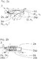
- Figure 2a Figure 12 is a schematic representation of an embodiment of the present invention using frustrated total internal reflection.
- the embodiment Figures 1a-1h supplemented with exemplary beam paths L.
- the multiple total reflection with particular expanded beams is shown schematically, with a homogeneous illumination of the embossing roller and the homogeneous decoupling of the radiation into the embossing compound 17 takes place.
- the embossing roller 2 includes the cylinder body 16, the end faces for coupling 2k, 2s and the mirrored end face 2sp. Without proportionality, the embossing compound 17 is shown symbolically, with the entry of the radiation also being shown.
- the inner lateral surface is mirrored or opaque to radiation due to total internal reflection.
- FIG 2b is a schematic representation of an embodiment according to the invention by means of impurity extraction.
- the embossing roller 2 disclosed according to the invention is used in an embodiment as shown in Figures 1a-1h is shown as an example used.
- the radiation is coupled in analogously to the previous figures.
- the beam path in the embossing roller is not shown in full.
- the embossing mass that touches the outer cylindrical surface of the embossing roller is not shown.
- the coupling of the beam is indicated with L.
- a stochastic beam path in the embossing roller is not shown.
- the outcoupling by means of imperfections 16s with statistically uniformly distributed outcoupling radiation cones is indicated only schematically.
- the homogeneity of the emitted radiation is determined by the parameters distribution, shape and size of the imperfections.
- the design of the imperfections is assumed to be known to the person skilled in the art. Impurities can be interpreted as scattering centers.
- the lateral surface 16a of the cylinder body 16 is not polished or lapped, that is to say it is produced with a high surface quality, but is provided with imperfections 16s. These can be designed in particular as a brushed surface. Targeted traces of structuring from sandblasting or etched grain boundaries can be present.
- the surface 16a may have stochastically evenly distributed, small-periodic deviations from the mathematically optimal shape of the surface, which should be in the magnitude of the radiation wavelength. A homogeneous illumination of the embossing compound can thus be achieved.
- the beam path of the radiation L should be as in Figure 2a be understood.
- Figure 3a is a schematic representation of the total reflection and the course of the intensity at a boundary surface G.
- the approaches of geometric optics are used here in a simplified manner.
- a light beam emerges from an optically denser medium M2 with the refractive index n2 into an optically thinner medium M1 with the refractive index n1
- ⁇ c critical angle
- ⁇ c critical angle
- FIG. 3b shows an intensity distribution of a totally reflected beam, where the intensity I is not shown to scale as a function of the normal distance x to the surface.
- the intensity of the totally reflected beam in the optically denser medium M2 is represented as constant with the quantity I2.
- Figure 3b is a schematic representation of the qualitative intensity profile I 1 of the evanescent wave and intensity profile I 2 of the totally reflected beam at an interface G.
- an object O with the refractive index n3 is present near the interface G at a distance k.
- the refractive index n1 is smaller than the refractive index n3. If the distance k is small enough (zero or greater), the object O with refractive index n3 is in the light skin. At least part of the radiation (provided the appropriate absorption properties are present) is absorbed in O. It is thus possible to decouple the totally reflected radiation from the medium M1 in O.
- An intensity distribution of a frustrated totally reflecting beam is only qualitatively 3d shown, where the intensity I is shown as a function of the propagation direction x.
- the intensity I 2 is considered to be constant.
- the intensity in the medium M1 with refractive index n1 is proportional to the reciprocal of the exponential function e.
- the residual intensity I 3 is coupled into the medium O and passed on in the medium O, assumed to be constant.
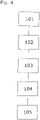
- FIG. 4 is a schematic block diagram of an imprint method according to the invention.
- the radiation is coupled into the embossing roller.
- step 102 contact of the embossing compound with the embossing roller is initiated.
- the radiation is coupled out of the embossing roller with simultaneous coupling of the radiation into the embossing compound. Curing is thus initiated.
- the embossing roller is separated from the embossing compound.
- step 105 the embossing roller is continuously cleaned and prepared for repeated embossing, so that step 101 in particular can be initiated again.
- Steps 101 and 102 can also be interchanged.
- FIG. 5 is a representation of the scheme of an imprint plant according to the invention.
- the imprint system 15 consists of a combination and coupling of the modules listed:
- the carrier material 5, in particular a carrier film runs through the embossing process from a transmitter module 1 to the receiver module 4.
- the embossing takes place on and/or in the embossing module 2, which is designed as an embossing roller 2 can be.
- An embossing force F acts, which is absorbed in particular by a support module 3, this being signaled with a counterforce F'.
- Drives 8 (motors with or without gears) can be used to generate the relative movement between the embossing mass and the embossing module, in particular the embossing roller.
- the carrier film with the embossing compound and the embossing roller can roll off one another.
- Other force or pressure generating elements 8 can generate the force (pressure). This can be done hydraulically and/or pneumatically and/or mechanically and/or electronically and/or electromagnetically.
- a radiation module 9 is coupled to the embossing module.
- at least one radiation source LED or LED array, or mercury vapor lamp, or halogen emitters, or laser, or magnetrons, or other transit time tubes
- beam-shaping elements such as mirrors, semi-transparent mirrors, lenses, prisms, light guides, screens, other auxiliary units such as cooling may be included.
- the carrier material 5 runs through a guiding and/or prestressing and/or joining module 10, which can contain sub-modules for cleaning and/or deionizing stations in order to counteract any static charging of the carrier and to remove any particles from the carrier .
- An upper coating module 6 and/or optionally a lower coating module 7 can follow as the next module.
- these modules can remove cover foils and expose the embossing compound.
- Modules 6 and 7 meter the embossing compound, shape, remove excess solvent and/or prepare for embossing.
- the embossing module 2 can be provided with the method according to the invention and auxiliary units.
- Downstream modules can follow, such as module 12 and module 13, which in particular can apply a protective layer and/or a protective film and/or can carry out complete curing.
- a further deionization station and/or a pre-tensioning and/or regulation and/or management module 11 can be connected in front of the receiver module 4 .
- the imprint system 15 can be controlled and influenced with a measuring and/or control and/or regulation module or modules 14, to maintain, for example, throughput, quality, process uniformity and stability.
- the networking of all modules with the control and/or regulation module 14 is symbolized with dashed lines.
- the imprint module 2 can integrate the drive module 8 and/or the radiation module 9 into itself. Furthermore, it is possible to combine the transmission module 1 with the guiding and/or prestressing and/or joining module 10 . Another possibility is the multiple integration of the transmission module 1 with the joining module 10 and with the coating modules 6 and/or the coating module 7. This applies analogously to the modules 11, 12, 13 and 4.
- both a functional separation and a functional integration are possible with the modular design, so that an imprint system 15 optimized for the function and/or costs is produced. Accordingly, in a further embodiment of the imprint system according to the invention, it is possible to contain only the embossing module 2 . Furthermore, in another embodiment according to the invention, a combination of the embossing module 2 with the control module 14 is conceivable. All combinatorial possibilities from at least one of the modules for the imprint system 15 (particularly module 2) should be considered disclosed.
Landscapes
- Physics & Mathematics (AREA)
- General Physics & Mathematics (AREA)
- Engineering & Computer Science (AREA)
- Chemical & Material Sciences (AREA)
- Nanotechnology (AREA)
- Plasma & Fusion (AREA)
- Condensed Matter Physics & Semiconductors (AREA)
- Manufacturing & Machinery (AREA)
- Crystallography & Structural Chemistry (AREA)
- Shaping Of Tube Ends By Bending Or Straightening (AREA)
- Exposure Of Semiconductors, Excluding Electron Or Ion Beam Exposure (AREA)
- Casting Or Compression Moulding Of Plastics Or The Like (AREA)
Claims (13)
- Procédé de marquage de microstructures et/ou nanostructures, présentant les étapes suivantes :- entrée d'un rayonnement de réticulation (L) dans un rouleau de marquage (2, 2′, 2ʺ, 2‴, 2ʺʺ, 2ʺ‴, 2‴‴, 2′‴‴) transparent au rayonnement de réticulation, en particulier structuré, de sorte que le rouleau de marquage (2, 2′, 2ʺ, 2‴, 2ʺʺ, 2ʺ‴, 2‴‴, 2′‴‴) sert de conducteur optique pour le rayonnement de réticulation (L) entré,- sortie du rayonnement de réticulation (L) hors du rouleau de marquage (2, 2′ 2ʺ, 2‴, 2ʺʺ, 2ʺ‴, 2‴‴, 2′‴‴),- durcissement d'une masse de marquage (17) sollicitée par le rouleau de marquage (2, 2′, 2ʺ, 2‴, 2ʺ, 2ʺ‴, 2‴‴, 2′‴‴) par le rayonnement de réticulation (L) sorti.
- Procédé selon la revendication 1, caractérisé en ce que le rayonnement de réticulation (L) est entré sur au moins une des faces avant (2k) du rouleau de marquage (2, 2′, 2ʺ, 2‴, 2ʺʺ, 2ʺ‴, 2‴‴, 2′‴‴).
- Procédé selon l'une des revendications précédentes, caractérisé en ce qu'au moins un module d'émission (1) fait entrer le rayonnement de réticulation (L) dans le rouleau de marquage (2, 2′, 2ʺ, 2‴, 2ʺʺ, 2ʺ‴, 2‴‴, 2′‴‴).
- Procédé selon l'une des revendications précédentes, caractérisé en ce que le rayonnement de réticulation (L) est un rayonnement UV.
- Procédé selon l'une des revendications précédentes, caractérisé en ce que plusieurs réflexions totales du rayonnement de réticulation (L) ont lieu à l'intérieur du rouleau de marquage (2, 2′, 2ʺ, 2‴, 2ʺʺ, 2ʺ‴, 2‴‴, 2′‴‴).
- Procédé selon l'une des revendications précédentes, caractérisé en ce que le rayonnement de réticulation (L) est sorti hors du rouleau de marquage (2, 2′, 2ʺ, 2‴, 2ʺʺ, 2ʺ‴, 2‴‴, 2′‴‴) au moyen de réflexion totale frustrée et entré parallèlement dans la masse de marquage (17) pour le durcissement.
- Procédé selon l'une des revendications précédentes, caractérisé en ce que le rayonnement de réticulation (L) est sorti par des points de diffusion (16s).
- Procédé selon l'une des revendications précédentes, caractérisé en ce que la masse de marquage (17) est formée au moyen du rouleau de marquage (2, 2′, 2ʺ, 2‴, 2ʺʺ, 2ʺ‴, 2‴‴, 2′‴‴) et le durcissement de la masse de marquage (17) a lieu avec un retard temporel minimal ou en même temps par le rayonnement de réticulation (L).
- Dispositif (15) de marquage de microstructures et/ou nanostructures, présentant :-- un module d'entrée (1) pour envoyer un rayonnement de réticulation (L),-- un rouleau de marquage (2, 2′, 2ʺ, 2‴, 2ʺʺ, 2‴, 2‴‴, 2′‴‴) transparent au rayonnement de réticulation,dans lequel le rayonnement de réticulation (L) peut être entré dans le rouleau de marquage (2, 2′, 2ʺ, 2‴, 2ʺʺ, 2ʺ‴, 2‴‴, 2′‴‴), de sorte que le rouleau de marquage (2, 2′, 2ʺ, 2‴, 2ʺʺ, 2ʺ‴, 2‴‴, 2′‴‴) puisse être utilisé en tant que conducteur optique pour le rayonnement de réticulation (L) entré, dans lequel le rayonnement de réticulation (L) peut être sorti hors du rouleau de marquage (2, 2′, 2ʺ, 2‴, 2ʺʺ, 2ʺ‴, 2‴‴, 2′‴‴) et une masse de marquage (17) sollicitée par le rouleau de marquage (2, 2′, 2ʺ, 2‴, 2ʺʺ, 2ʺ‴, 2‴‴, 2′‴‴) peut être durcie par le rayonnement de réticulation (L) sorti.
- Rouleau de marquage (2, 2′, 2ʺ, 2‴, 2ʺʺ, 2ʺ‴, 2‴‴, 2′‴‴) configuré de façon à ce qu'un procédé selon la revendication 1 puisse être exécuté.
- Rouleau de marquage (2, 2′, 2ʺ, 2‴, 2ʺʺ, 2ʺ‴, 2‴‴, 2′‴‴) selon la revendication 10, dans lequel une surface d'enveloppe intérieure (2ik) du rouleau de marquage (2, 2′, 2ʺ, 2‴, 2ʺʺ, 2ʺ‴, 2‴‴, 2′‴‴) est conique.
- Rouleau de marquage (2, 2′, 2ʺ, 2‴, 2ʺʺ, 2ʺ‴, 2‴‴, 2′‴‴) selon la revendication 10, dans lequel au moins une des faces avant (2s, 2sk) du rouleau de marquage (2, 2′, 2ʺ, 2‴, 2ʺʺ, 2ʺ‴, 2‴‴, 2′‴‴) est dotée de miroirs réfléchissants et/ou de nervures et/ou d'encoches pour l'entrée du rayonnement.
- Rouleau de marquage (2, 2′, 2ʺ, 2‴, 2ʺʺ, 2ʺ‴, 2‴‴, 2‴‴′) selon la revendication 10, dans lequel le rayonnement de réticulation (L) peut être entré d'un côté dans une face avant (2s, 2sk) du rouleau de marquage (2, 2′, 2ʺ, 2‴, 2ʺʺ, 2‴ʺ, 2‴‴, 2′‴‴) et la face avant (2sp) opposée est totalement dotée de miroirs réfléchissants.
Applications Claiming Priority (2)
| Application Number | Priority Date | Filing Date | Title |
|---|---|---|---|
| DE102016123538.5A DE102016123538A1 (de) | 2016-12-06 | 2016-12-06 | Verfahren zum Prägen von Mikro- und/oder Nanostrukturen |
| PCT/EP2017/076978 WO2018103940A1 (fr) | 2016-12-06 | 2017-10-23 | Procédé pour imprimer des micro- et/ou nanostructures |
Publications (3)
| Publication Number | Publication Date |
|---|---|
| EP3552058A1 EP3552058A1 (fr) | 2019-10-16 |
| EP3552058B1 true EP3552058B1 (fr) | 2022-07-20 |
| EP3552058B9 EP3552058B9 (fr) | 2022-09-28 |
Family
ID=60186272
Family Applications (1)
| Application Number | Title | Priority Date | Filing Date |
|---|---|---|---|
| EP17791041.1A Active EP3552058B9 (fr) | 2016-12-06 | 2017-10-23 | Procédé, appareil et rouleau d'impression pour imprimer des micro- et/ou nanostructures |
Country Status (7)
| Country | Link |
|---|---|
| US (1) | US11040525B2 (fr) |
| EP (1) | EP3552058B9 (fr) |
| JP (1) | JP6998377B2 (fr) |
| KR (1) | KR102487231B1 (fr) |
| CN (1) | CN109997078B (fr) |
| DE (1) | DE102016123538A1 (fr) |
| WO (1) | WO2018103940A1 (fr) |
Families Citing this family (2)
| Publication number | Priority date | Publication date | Assignee | Title |
|---|---|---|---|---|
| DE102018114009A1 (de) * | 2018-06-12 | 2019-12-12 | Volkswagen Aktiengesellschaft | Aktivmaterialkörper für einen Akkumulator |
| JP7419516B2 (ja) * | 2019-11-19 | 2024-01-22 | エーファウ・グループ・エー・タルナー・ゲーエムベーハー | マイクロパターンおよび/またはナノパターンをエンボス加工する装置および方法 |
Family Cites Families (14)
| Publication number | Priority date | Publication date | Assignee | Title |
|---|---|---|---|---|
| DE69405451T2 (de) | 1993-03-16 | 1998-03-12 | Koninkl Philips Electronics Nv | Verfahren und Vorrichtung zur Herstellung eines strukturierten Reliefbildes aus vernetztem Photoresist auf einer flachen Substratoberfläche |
| JP2005085965A (ja) | 2003-09-08 | 2005-03-31 | Canon Inc | 近接場露光用マスク、近接場露光方法、及び近接場露光装置 |
| US20080229950A1 (en) * | 2007-03-19 | 2008-09-25 | Ping Mei | Seamless imprint roller and method of making |
| US8071277B2 (en) * | 2007-12-21 | 2011-12-06 | 3M Innovative Properties Company | Method and system for fabricating three-dimensional structures with sub-micron and micron features |
| US8518633B2 (en) * | 2008-01-22 | 2013-08-27 | Rolith Inc. | Large area nanopatterning method and apparatus |
| JP2010199401A (ja) | 2009-02-26 | 2010-09-09 | Hitachi Maxell Ltd | 成形体の製造方法及び製造装置 |
| NL2005254A (en) * | 2009-09-22 | 2011-03-23 | Asml Netherlands Bv | Imprint lithography method and apparatus. |
| KR100988935B1 (ko) * | 2009-10-28 | 2010-10-20 | 한국기계연구원 | 롤 임프린트 장치 |
| JP2012061832A (ja) | 2010-09-17 | 2012-03-29 | Sony Corp | 積層体の製造方法、原盤および転写装置 |
| CN102441989A (zh) * | 2010-09-17 | 2012-05-09 | 索尼公司 | 层叠体及其制造方法、转印装置、成型元件以及光学元件 |
| JP5730449B2 (ja) | 2011-12-06 | 2015-06-10 | エーファウ・グループ・エー・タルナー・ゲーエムベーハー | ナノ構造スタンプ、型押しロール、ナノ構造部を連続型押しする装置および方法 |
| JP2013207060A (ja) | 2012-03-28 | 2013-10-07 | Sony Corp | 構造物形成装置、構造物の製造方法及び構造物 |
| KR102243425B1 (ko) * | 2012-05-02 | 2021-04-22 | 메타머트리얼 테크놀러지스 유에스에이, 인크. | 원통형 고분자 마스크 및 제작 방법 |
| DE102015120535A1 (de) * | 2015-11-26 | 2017-06-01 | Leibniz-Institut für Oberflächenmodifizierung e.V. | Vorrichtung und Verfahren zur Herstellung einer beidseitig mikrostrukturierten Folie |
-
2016
- 2016-12-06 DE DE102016123538.5A patent/DE102016123538A1/de not_active Ceased
-
2017
- 2017-10-23 US US16/463,092 patent/US11040525B2/en active Active
- 2017-10-23 JP JP2019528677A patent/JP6998377B2/ja active Active
- 2017-10-23 WO PCT/EP2017/076978 patent/WO2018103940A1/fr not_active Ceased
- 2017-10-23 CN CN201780074292.5A patent/CN109997078B/zh active Active
- 2017-10-23 EP EP17791041.1A patent/EP3552058B9/fr active Active
- 2017-10-23 KR KR1020197013680A patent/KR102487231B1/ko active Active
Also Published As
| Publication number | Publication date |
|---|---|
| US11040525B2 (en) | 2021-06-22 |
| CN109997078B (zh) | 2023-03-31 |
| CN109997078A (zh) | 2019-07-09 |
| WO2018103940A1 (fr) | 2018-06-14 |
| KR102487231B1 (ko) | 2023-01-10 |
| US20200070496A1 (en) | 2020-03-05 |
| JP2020513690A (ja) | 2020-05-14 |
| KR20190090792A (ko) | 2019-08-02 |
| DE102016123538A1 (de) | 2018-06-07 |
| EP3552058B9 (fr) | 2022-09-28 |
| JP6998377B2 (ja) | 2022-01-18 |
| EP3552058A1 (fr) | 2019-10-16 |
Similar Documents
| Publication | Publication Date | Title |
|---|---|---|
| DE69027228T2 (de) | Mikrostruktur aufweisende Kunststoff-Verbundkörper und Verfahren zur Herstellung | |
| Rank et al. | High‐speed roll‐to‐roll hot embossing of micrometer and sub micrometer structures using seamless direct laser interference patterning treated sleeves | |
| DE10346124A1 (de) | Werkzeug zur Erzeugen von mikrostrukturierten Oberflächen | |
| Lang et al. | Large area one‐step fabrication of three‐level multiple‐scaled micro and nanostructured nickel sleeves for roll‐to‐roll hot embossing | |
| DE112010004165T5 (de) | Walzendruckvorrichtung | |
| EP3552058B9 (fr) | Procédé, appareil et rouleau d'impression pour imprimer des micro- et/ou nanostructures | |
| WO2018041371A1 (fr) | Installation et procédé pour imprimer des micro- et/ou nanostructures | |
| WO2020182934A1 (fr) | Procédé et dispositif pour placer un matériau sur un support | |
| EP2353050A1 (fr) | Procédé et dispositif de production d'hologrammes de transmission et/ou de réflexion volumiques | |
| DE10106888B4 (de) | Verfahren und Vorrichtung zur Herstellung einer Oberflächenbeschichtung | |
| EP3134771B1 (fr) | Procédé et dispositif de marquage d'une nanostructure | |
| Elkarkri et al. | Laser photonic nanojets triggered thermoplasmonic micro/nanofabrication of polymer materials for enhanced resolution | |
| Tsai et al. | Fabrication of seamless roller mold with 3D micropatterns using inner curved surface photolithography | |
| EP3083251B1 (fr) | Disposititif et procédé de production de surfaces structurées | |
| DE102012207231A1 (de) | Prägeverfahren und ein mittels des Prägeverfahrens hergestelltes Werkstück | |
| Lang et al. | Direct laser interference patterning of metallic sleeves for roll-to-roll hot embossing | |
| EP3517654B1 (fr) | Procédé de fabrication d'un insert de moule à (sous-)microstructures ainsi que pièce à usiner à (sous-)microstructures | |
| DE102013107909B4 (de) | Verfahren und Anlage zum Einprägen einer Struktur auf einem mit einem Lack beschichteten Substrat | |
| EP3555705B1 (fr) | Dispositif et procédé de réalisation de nanostructures périodiques de grande surface sur un substrat planaire au moyen d'un procédé de nano-impression | |
| YOSHINO et al. | 3250 Development of nanostructured foil mold for roller nano imprint process | |
| KR20230043836A (ko) | 텍스처를 복제하기 위한 장치 및 방법 | |
| WO2006133956A2 (fr) | Elimination de minces couches polymeriques structurees par du plasma atmospherique | |
| DE102017121097A1 (de) | Mikrostrukturierung von gebogenen Flächen durch UV-Lithographie |
Legal Events
| Date | Code | Title | Description |
|---|---|---|---|
| STAA | Information on the status of an ep patent application or granted ep patent |
Free format text: STATUS: UNKNOWN |
|
| STAA | Information on the status of an ep patent application or granted ep patent |
Free format text: STATUS: THE INTERNATIONAL PUBLICATION HAS BEEN MADE |
|
| PUAI | Public reference made under article 153(3) epc to a published international application that has entered the european phase |
Free format text: ORIGINAL CODE: 0009012 |
|
| STAA | Information on the status of an ep patent application or granted ep patent |
Free format text: STATUS: REQUEST FOR EXAMINATION WAS MADE |
|
| 17P | Request for examination filed |
Effective date: 20190704 |
|
| AK | Designated contracting states |
Kind code of ref document: A1 Designated state(s): AL AT BE BG CH CY CZ DE DK EE ES FI FR GB GR HR HU IE IS IT LI LT LU LV MC MK MT NL NO PL PT RO RS SE SI SK SM TR |
|
| AX | Request for extension of the european patent |
Extension state: BA ME |
|
| DAV | Request for validation of the european patent (deleted) | ||
| DAX | Request for extension of the european patent (deleted) | ||
| GRAP | Despatch of communication of intention to grant a patent |
Free format text: ORIGINAL CODE: EPIDOSNIGR1 |
|
| STAA | Information on the status of an ep patent application or granted ep patent |
Free format text: STATUS: GRANT OF PATENT IS INTENDED |
|
| INTG | Intention to grant announced |
Effective date: 20220422 |
|
| GRAS | Grant fee paid |
Free format text: ORIGINAL CODE: EPIDOSNIGR3 |
|
| GRAA | (expected) grant |
Free format text: ORIGINAL CODE: 0009210 |
|
| STAA | Information on the status of an ep patent application or granted ep patent |
Free format text: STATUS: THE PATENT HAS BEEN GRANTED |
|
| AK | Designated contracting states |
Kind code of ref document: B1 Designated state(s): AL AT BE BG CH CY CZ DE DK EE ES FI FR GB GR HR HU IE IS IT LI LT LU LV MC MK MT NL NO PL PT RO RS SE SI SK SM TR |
|
| REG | Reference to a national code |
Ref country code: CH Ref legal event code: EP |
|
| REG | Reference to a national code |
Ref country code: DE Ref legal event code: R096 Ref document number: 502017013504 Country of ref document: DE |
|
| REG | Reference to a national code |
Ref country code: AT Ref legal event code: REF Ref document number: 1505905 Country of ref document: AT Kind code of ref document: T Effective date: 20220815 |
|
| REG | Reference to a national code |
Ref country code: IE Ref legal event code: FG4D Free format text: LANGUAGE OF EP DOCUMENT: GERMAN Ref country code: CH Ref legal event code: PK Free format text: BERICHTIGUNG B9 |
|
| REG | Reference to a national code |
Ref country code: LT Ref legal event code: MG9D |
|
| REG | Reference to a national code |
Ref country code: NL Ref legal event code: MP Effective date: 20220720 |
|
| PG25 | Lapsed in a contracting state [announced via postgrant information from national office to epo] |
Ref country code: SE Free format text: LAPSE BECAUSE OF FAILURE TO SUBMIT A TRANSLATION OF THE DESCRIPTION OR TO PAY THE FEE WITHIN THE PRESCRIBED TIME-LIMIT Effective date: 20220720 Ref country code: RS Free format text: LAPSE BECAUSE OF FAILURE TO SUBMIT A TRANSLATION OF THE DESCRIPTION OR TO PAY THE FEE WITHIN THE PRESCRIBED TIME-LIMIT Effective date: 20220720 Ref country code: PT Free format text: LAPSE BECAUSE OF FAILURE TO SUBMIT A TRANSLATION OF THE DESCRIPTION OR TO PAY THE FEE WITHIN THE PRESCRIBED TIME-LIMIT Effective date: 20221121 Ref country code: NO Free format text: LAPSE BECAUSE OF FAILURE TO SUBMIT A TRANSLATION OF THE DESCRIPTION OR TO PAY THE FEE WITHIN THE PRESCRIBED TIME-LIMIT Effective date: 20221020 Ref country code: NL Free format text: LAPSE BECAUSE OF FAILURE TO SUBMIT A TRANSLATION OF THE DESCRIPTION OR TO PAY THE FEE WITHIN THE PRESCRIBED TIME-LIMIT Effective date: 20220720 Ref country code: LV Free format text: LAPSE BECAUSE OF FAILURE TO SUBMIT A TRANSLATION OF THE DESCRIPTION OR TO PAY THE FEE WITHIN THE PRESCRIBED TIME-LIMIT Effective date: 20220720 Ref country code: LT Free format text: LAPSE BECAUSE OF FAILURE TO SUBMIT A TRANSLATION OF THE DESCRIPTION OR TO PAY THE FEE WITHIN THE PRESCRIBED TIME-LIMIT Effective date: 20220720 Ref country code: FI Free format text: LAPSE BECAUSE OF FAILURE TO SUBMIT A TRANSLATION OF THE DESCRIPTION OR TO PAY THE FEE WITHIN THE PRESCRIBED TIME-LIMIT Effective date: 20220720 Ref country code: ES Free format text: LAPSE BECAUSE OF FAILURE TO SUBMIT A TRANSLATION OF THE DESCRIPTION OR TO PAY THE FEE WITHIN THE PRESCRIBED TIME-LIMIT Effective date: 20220720 |
|
| PG25 | Lapsed in a contracting state [announced via postgrant information from national office to epo] |
Ref country code: PL Free format text: LAPSE BECAUSE OF FAILURE TO SUBMIT A TRANSLATION OF THE DESCRIPTION OR TO PAY THE FEE WITHIN THE PRESCRIBED TIME-LIMIT Effective date: 20220720 Ref country code: IS Free format text: LAPSE BECAUSE OF FAILURE TO SUBMIT A TRANSLATION OF THE DESCRIPTION OR TO PAY THE FEE WITHIN THE PRESCRIBED TIME-LIMIT Effective date: 20221120 Ref country code: HR Free format text: LAPSE BECAUSE OF FAILURE TO SUBMIT A TRANSLATION OF THE DESCRIPTION OR TO PAY THE FEE WITHIN THE PRESCRIBED TIME-LIMIT Effective date: 20220720 Ref country code: GR Free format text: LAPSE BECAUSE OF FAILURE TO SUBMIT A TRANSLATION OF THE DESCRIPTION OR TO PAY THE FEE WITHIN THE PRESCRIBED TIME-LIMIT Effective date: 20221021 |
|
| REG | Reference to a national code |
Ref country code: DE Ref legal event code: R097 Ref document number: 502017013504 Country of ref document: DE |
|
| PG25 | Lapsed in a contracting state [announced via postgrant information from national office to epo] |
Ref country code: SM Free format text: LAPSE BECAUSE OF FAILURE TO SUBMIT A TRANSLATION OF THE DESCRIPTION OR TO PAY THE FEE WITHIN THE PRESCRIBED TIME-LIMIT Effective date: 20220720 Ref country code: RO Free format text: LAPSE BECAUSE OF FAILURE TO SUBMIT A TRANSLATION OF THE DESCRIPTION OR TO PAY THE FEE WITHIN THE PRESCRIBED TIME-LIMIT Effective date: 20220720 Ref country code: DK Free format text: LAPSE BECAUSE OF FAILURE TO SUBMIT A TRANSLATION OF THE DESCRIPTION OR TO PAY THE FEE WITHIN THE PRESCRIBED TIME-LIMIT Effective date: 20220720 Ref country code: CZ Free format text: LAPSE BECAUSE OF FAILURE TO SUBMIT A TRANSLATION OF THE DESCRIPTION OR TO PAY THE FEE WITHIN THE PRESCRIBED TIME-LIMIT Effective date: 20220720 |
|
| PLBE | No opposition filed within time limit |
Free format text: ORIGINAL CODE: 0009261 |
|
| STAA | Information on the status of an ep patent application or granted ep patent |
Free format text: STATUS: NO OPPOSITION FILED WITHIN TIME LIMIT |
|
| PG25 | Lapsed in a contracting state [announced via postgrant information from national office to epo] |
Ref country code: SK Free format text: LAPSE BECAUSE OF FAILURE TO SUBMIT A TRANSLATION OF THE DESCRIPTION OR TO PAY THE FEE WITHIN THE PRESCRIBED TIME-LIMIT Effective date: 20220720 Ref country code: MC Free format text: LAPSE BECAUSE OF FAILURE TO SUBMIT A TRANSLATION OF THE DESCRIPTION OR TO PAY THE FEE WITHIN THE PRESCRIBED TIME-LIMIT Effective date: 20220720 Ref country code: EE Free format text: LAPSE BECAUSE OF FAILURE TO SUBMIT A TRANSLATION OF THE DESCRIPTION OR TO PAY THE FEE WITHIN THE PRESCRIBED TIME-LIMIT Effective date: 20220720 |
|
| REG | Reference to a national code |
Ref country code: CH Ref legal event code: PL |
|
| REG | Reference to a national code |
Ref country code: BE Ref legal event code: MM Effective date: 20221031 |
|
| 26N | No opposition filed |
Effective date: 20230421 |
|
| GBPC | Gb: european patent ceased through non-payment of renewal fee |
Effective date: 20221023 |
|
| PG25 | Lapsed in a contracting state [announced via postgrant information from national office to epo] |
Ref country code: LU Free format text: LAPSE BECAUSE OF NON-PAYMENT OF DUE FEES Effective date: 20221023 Ref country code: AL Free format text: LAPSE BECAUSE OF FAILURE TO SUBMIT A TRANSLATION OF THE DESCRIPTION OR TO PAY THE FEE WITHIN THE PRESCRIBED TIME-LIMIT Effective date: 20220720 |
|
| PG25 | Lapsed in a contracting state [announced via postgrant information from national office to epo] |
Ref country code: LI Free format text: LAPSE BECAUSE OF NON-PAYMENT OF DUE FEES Effective date: 20221031 Ref country code: FR Free format text: LAPSE BECAUSE OF NON-PAYMENT OF DUE FEES Effective date: 20221031 Ref country code: CH Free format text: LAPSE BECAUSE OF NON-PAYMENT OF DUE FEES Effective date: 20221031 |
|
| PG25 | Lapsed in a contracting state [announced via postgrant information from national office to epo] |
Ref country code: SI Free format text: LAPSE BECAUSE OF FAILURE TO SUBMIT A TRANSLATION OF THE DESCRIPTION OR TO PAY THE FEE WITHIN THE PRESCRIBED TIME-LIMIT Effective date: 20220720 |
|
| PG25 | Lapsed in a contracting state [announced via postgrant information from national office to epo] |
Ref country code: BE Free format text: LAPSE BECAUSE OF NON-PAYMENT OF DUE FEES Effective date: 20221031 |
|
| PG25 | Lapsed in a contracting state [announced via postgrant information from national office to epo] |
Ref country code: IE Free format text: LAPSE BECAUSE OF NON-PAYMENT OF DUE FEES Effective date: 20221023 Ref country code: GB Free format text: LAPSE BECAUSE OF NON-PAYMENT OF DUE FEES Effective date: 20221023 |
|
| PG25 | Lapsed in a contracting state [announced via postgrant information from national office to epo] |
Ref country code: HU Free format text: LAPSE BECAUSE OF FAILURE TO SUBMIT A TRANSLATION OF THE DESCRIPTION OR TO PAY THE FEE WITHIN THE PRESCRIBED TIME-LIMIT; INVALID AB INITIO Effective date: 20171023 |
|
| PG25 | Lapsed in a contracting state [announced via postgrant information from national office to epo] |
Ref country code: CY Free format text: LAPSE BECAUSE OF FAILURE TO SUBMIT A TRANSLATION OF THE DESCRIPTION OR TO PAY THE FEE WITHIN THE PRESCRIBED TIME-LIMIT Effective date: 20220720 |
|
| PG25 | Lapsed in a contracting state [announced via postgrant information from national office to epo] |
Ref country code: MK Free format text: LAPSE BECAUSE OF FAILURE TO SUBMIT A TRANSLATION OF THE DESCRIPTION OR TO PAY THE FEE WITHIN THE PRESCRIBED TIME-LIMIT Effective date: 20220720 Ref country code: IT Free format text: LAPSE BECAUSE OF FAILURE TO SUBMIT A TRANSLATION OF THE DESCRIPTION OR TO PAY THE FEE WITHIN THE PRESCRIBED TIME-LIMIT Effective date: 20220720 |
|
| PG25 | Lapsed in a contracting state [announced via postgrant information from national office to epo] |
Ref country code: BG Free format text: LAPSE BECAUSE OF FAILURE TO SUBMIT A TRANSLATION OF THE DESCRIPTION OR TO PAY THE FEE WITHIN THE PRESCRIBED TIME-LIMIT Effective date: 20220720 |
|
| PG25 | Lapsed in a contracting state [announced via postgrant information from national office to epo] |
Ref country code: MT Free format text: LAPSE BECAUSE OF FAILURE TO SUBMIT A TRANSLATION OF THE DESCRIPTION OR TO PAY THE FEE WITHIN THE PRESCRIBED TIME-LIMIT Effective date: 20220720 |
|
| PG25 | Lapsed in a contracting state [announced via postgrant information from national office to epo] |
Ref country code: TR Free format text: LAPSE BECAUSE OF FAILURE TO SUBMIT A TRANSLATION OF THE DESCRIPTION OR TO PAY THE FEE WITHIN THE PRESCRIBED TIME-LIMIT Effective date: 20220720 |
|
| PGFP | Annual fee paid to national office [announced via postgrant information from national office to epo] |
Ref country code: DE Payment date: 20251020 Year of fee payment: 9 |
|
| PGFP | Annual fee paid to national office [announced via postgrant information from national office to epo] |
Ref country code: AT Payment date: 20251021 Year of fee payment: 9 |