EP3550630A1 - Method for packaging organic semiconductor device - Google Patents
Method for packaging organic semiconductor device Download PDFInfo
- Publication number
- EP3550630A1 EP3550630A1 EP16923065.3A EP16923065A EP3550630A1 EP 3550630 A1 EP3550630 A1 EP 3550630A1 EP 16923065 A EP16923065 A EP 16923065A EP 3550630 A1 EP3550630 A1 EP 3550630A1
- Authority
- EP
- European Patent Office
- Prior art keywords
- semiconductor device
- organic semiconductor
- layer
- photoresist
- organic
- Prior art date
- Legal status (The legal status is an assumption and is not a legal conclusion. Google has not performed a legal analysis and makes no representation as to the accuracy of the status listed.)
- Granted
Links
Images

Classifications
-
- H—ELECTRICITY
- H10—SEMICONDUCTOR DEVICES; ELECTRIC SOLID-STATE DEVICES NOT OTHERWISE PROVIDED FOR
- H10K—ORGANIC ELECTRIC SOLID-STATE DEVICES
- H10K50/00—Organic light-emitting devices
- H10K50/80—Constructional details
- H10K50/84—Passivation; Containers; Encapsulations
- H10K50/844—Encapsulations
- H10K50/8445—Encapsulations multilayered coatings having a repetitive structure, e.g. having multiple organic-inorganic bilayers
-
- H—ELECTRICITY
- H10—SEMICONDUCTOR DEVICES; ELECTRIC SOLID-STATE DEVICES NOT OTHERWISE PROVIDED FOR
- H10K—ORGANIC ELECTRIC SOLID-STATE DEVICES
- H10K50/00—Organic light-emitting devices
- H10K50/80—Constructional details
- H10K50/84—Passivation; Containers; Encapsulations
- H10K50/844—Encapsulations
-
- H—ELECTRICITY
- H10—SEMICONDUCTOR DEVICES; ELECTRIC SOLID-STATE DEVICES NOT OTHERWISE PROVIDED FOR
- H10K—ORGANIC ELECTRIC SOLID-STATE DEVICES
- H10K71/00—Manufacture or treatment specially adapted for the organic devices covered by this subclass
-
- H—ELECTRICITY
- H10—SEMICONDUCTOR DEVICES; ELECTRIC SOLID-STATE DEVICES NOT OTHERWISE PROVIDED FOR
- H10K—ORGANIC ELECTRIC SOLID-STATE DEVICES
- H10K71/00—Manufacture or treatment specially adapted for the organic devices covered by this subclass
- H10K71/20—Changing the shape of the active layer in the devices, e.g. patterning
- H10K71/231—Changing the shape of the active layer in the devices, e.g. patterning by etching of existing layers
- H10K71/233—Changing the shape of the active layer in the devices, e.g. patterning by etching of existing layers by photolithographic etching
-
- H—ELECTRICITY
- H10—SEMICONDUCTOR DEVICES; ELECTRIC SOLID-STATE DEVICES NOT OTHERWISE PROVIDED FOR
- H10K—ORGANIC ELECTRIC SOLID-STATE DEVICES
- H10K77/00—Constructional details of devices covered by this subclass and not covered by groups H10K10/80, H10K30/80, H10K50/80 or H10K59/80
- H10K77/10—Substrates, e.g. flexible substrates
- H10K77/111—Flexible substrates
-
- H—ELECTRICITY
- H10—SEMICONDUCTOR DEVICES; ELECTRIC SOLID-STATE DEVICES NOT OTHERWISE PROVIDED FOR
- H10K—ORGANIC ELECTRIC SOLID-STATE DEVICES
- H10K2102/00—Constructional details relating to the organic devices covered by this subclass
-
- H—ELECTRICITY
- H10—SEMICONDUCTOR DEVICES; ELECTRIC SOLID-STATE DEVICES NOT OTHERWISE PROVIDED FOR
- H10K—ORGANIC ELECTRIC SOLID-STATE DEVICES
- H10K2102/00—Constructional details relating to the organic devices covered by this subclass
- H10K2102/301—Details of OLEDs
- H10K2102/311—Flexible OLED
-
- Y—GENERAL TAGGING OF NEW TECHNOLOGICAL DEVELOPMENTS; GENERAL TAGGING OF CROSS-SECTIONAL TECHNOLOGIES SPANNING OVER SEVERAL SECTIONS OF THE IPC; TECHNICAL SUBJECTS COVERED BY FORMER USPC CROSS-REFERENCE ART COLLECTIONS [XRACs] AND DIGESTS
- Y02—TECHNOLOGIES OR APPLICATIONS FOR MITIGATION OR ADAPTATION AGAINST CLIMATE CHANGE
- Y02E—REDUCTION OF GREENHOUSE GAS [GHG] EMISSIONS, RELATED TO ENERGY GENERATION, TRANSMISSION OR DISTRIBUTION
- Y02E10/00—Energy generation through renewable energy sources
- Y02E10/50—Photovoltaic [PV] energy
- Y02E10/549—Organic PV cells
-
- Y—GENERAL TAGGING OF NEW TECHNOLOGICAL DEVELOPMENTS; GENERAL TAGGING OF CROSS-SECTIONAL TECHNOLOGIES SPANNING OVER SEVERAL SECTIONS OF THE IPC; TECHNICAL SUBJECTS COVERED BY FORMER USPC CROSS-REFERENCE ART COLLECTIONS [XRACs] AND DIGESTS
- Y02—TECHNOLOGIES OR APPLICATIONS FOR MITIGATION OR ADAPTATION AGAINST CLIMATE CHANGE
- Y02P—CLIMATE CHANGE MITIGATION TECHNOLOGIES IN THE PRODUCTION OR PROCESSING OF GOODS
- Y02P70/00—Climate change mitigation technologies in the production process for final industrial or consumer products
- Y02P70/50—Manufacturing or production processes characterised by the final manufactured product
Definitions
- the present invention is related to a device packaging technology field, and more particularly to a packaging method for organic semiconductor device.
- OLED Organic Light Emitting Diode
- the OLED display device has properties of self-luminous, wide viewing angle (up to 175°), short response time (1 ⁇ s), high luminous efficiency, wide color gamut, low operation voltage (3 ⁇ 10V), thin panel (less than 1mm), capable of manufacturing a large size, capable of manufacturing flexible panel and simple in process.
- the OLED device has a potential for low cost.
- the purpose of the present is to provide a packaging method for organic semiconductor device which can effectively block the moisture and oxygen in the external environment.
- a packaging method for organic semiconductor device comprising steps of: manufacturing an organic semiconductor device on a flexible base; forming a photoresist block having a predetermined interval with respect to the organic semiconductor device and located at two sides of the organic semiconductor device on the flexible base; depositing an inorganic layer on the photoresist blocks, the organic semiconductor device and the flexible base; removing the photoresist block and the inorganic layer on the photoresist block; and depositing an organic layer on the inorganic layer disposed on the organic semiconductor device.
- the step of forming a photoresist block comprises steps of: coating a photoresist layer on the organic semiconductor device and the flexible base; using a predetermined mask plate to perform an exposure to the photoresist layer, wherein, the mask plate includes a light-shielding portion and a light-transmitting portion respectively located at two sides of the light-shielding portion, the light-shielding portion is corresponding to the organic semiconductor device, and two sides of the light-shielding portion are respectively exceeded two sides of the organic semiconductor device; and developing the photoresist layer after being exposed in order to remove the photoresist layer corresponding to the light-shielding portion so as to form a photoresist block.
- PECVD Plasma Enhanced Chemical Vapor Deposition
- PLD Pulsed Laser Deposition
- sputter deposition method to deposit the inorganic layer.
- the inorganic layer includes at least one of Al 2 O 3 , TiO 2 , SiN x , SiCN x , SiO x , and ZrO 2 .
- IJP inkjet printing forming method
- PECVD Plasma Enhanced Chemical Vapor Deposition
- slot extrusion coating method to manufacture the organic layer.
- the organic layer includes at least one of acrylate, hexamethyldisiloxane, polyacrylate, polycarbonate and polystyrene.
- the step of removing the photoresist block and the inorganic layer on the photoresist block comprises: immersing in an organic solvent for a predetermined time such that the photoresist block is detached from the flexible base.
- the packaging method according to an embodiment of the present invention can form an inorganic/organic flexible OLED packaging structure.
- the packaging structure cannot only omit a deposition mask used in depositing an inorganic layer in the conventional thin-film packaging art, but also effectively increase a blocking property of moisture and oxygen of OLED device in order to increase the life of the OLED device.
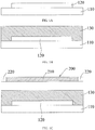
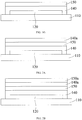
- FIG. 1A to FIG. 1G are flow charts of a packaging method for organic semiconductor device according to an embodiment of the present invention.
- the flexible base 110 is made of a flexible material such as polyethylene naphthalate (PEN).
- PEN polyethylene naphthalate
- the organic semiconductor device 120 can be an OLED device, but the present invention is not limited.
- coating a photoresist layer 130 on the organic semiconductor device 120 and the flexible base 110 Specifically, using a spin-coater to coat a polymer photoresist including fluorine on the flexible base 110 and the organic semiconductor device 120. Baking for 10 min in the temperature of 80°C in order to form the photoresist layer 130.
- the mask plate 200 includes a light-shielding portion 210 and a light-transmitting portion 220 respectively located at two sides of the light-shielding portion 210.
- the light-shielding portion 210 is corresponding to the organic semiconductor device 120, and two sides of the light-shielding portion 210 are respectively exceeded two sides of the organic semiconductor device 120. That is, a projection of the organic semiconductor device 120 on the light-shielding portion 210 is fully inside the light-shielding portion 210.
- the photoresist block 130a having a predetermined interval with respect to the organic semiconductor device 120 and located at two sides of the organic semiconductor device 120 disposed on the flexible base 110 are formed.
- the inorganic layer 140 can be made by at least one of Al 2 O 3 , TiO 2 , SiN x , SiCN x , SiO x , and ZrO 2 .
- the present invention is not limited.
- the inorganic layer 140 can also be made of an inorganic material having a high water and oxygen resistance effect.
- removing the photoresist block 130a and the inorganic layer 140 on the photoresist block 130a Specifically, immersing in an organic solvent for 1 ⁇ 30 min. At this time, the photoresist block 130a will detach from the flexible base 110, and other parts (such as the organic semiconductor device 120, the inorganic layer 140 on the organic semiconductor device 120, the inorganic layer 140 on the flexible base 110) will be remained in order to remove the photoresist block 130a and the inorganic layer 140 on the photoresist block 130a.
- the organic layer 150 can adopt at least one of acrylate, hexamethyldisiloxane, polyacrylate, polycarbonate and polystyrene, but the present invention is not limited.
- the organic layer 150 can also adopt an organic material that can buffer a stress when the device is bent or folded in order to avoid particle contaminant from covering.
- the packaging method according to an embodiment of the present invention can form an inorganic/organic flexible OLED packaging structure.
- the packaging structure cannot only omit a deposition mask used in depositing an inorganic layer in the conventional thin-film packaging art, but also effectively increase a blocking property of moisture and oxygen of OLED device in order to increase the life of the OLED device.
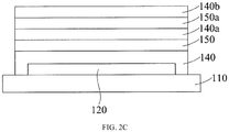
- FIG. 2A to FIG. 2C are flow charts of a packaging method for organic semiconductor device according to another embodiment of the present invention.
- the present invention further includes a packaging method shown in FIG. 2A to FIG. 2C .
- the inorganic layer 140a can be made of at least one of Al 2 O 3 , TiO 2 , SiN x , SiCN x , SiO x , and ZrO 2 , but the present invention is not limited.
- the inorganic layer 140a can also be made of an inorganic material having a high water and oxygen resistance effect.
- the organic layer 150a can adopt at least one of acrylate, hexamethyldisiloxane, polyacrylate, polycarbonate and polystyrene, but the present invention is not limited.
- the organic layer 150a can also adopt an organic material that can buffer a stress when the device is bent or folded in order to avoid particle contaminant from covering.
- the inorganic layer 140b can be made of at least one of Al 2 O 3 , TiO 2 , SiN x , SiCN x , SiO x , and ZrO 2 , but the present invention is not limited.
- the inorganic layer 140b can also be made of an inorganic material having a high water and oxygen resistance effect.
Landscapes
- Physics & Mathematics (AREA)
- Optics & Photonics (AREA)
- Chemical & Material Sciences (AREA)
- Inorganic Chemistry (AREA)
- Engineering & Computer Science (AREA)
- Manufacturing & Machinery (AREA)
- Electroluminescent Light Sources (AREA)
Abstract
Description
- The present invention is related to a device packaging technology field, and more particularly to a packaging method for organic semiconductor device.
- In the recent years, Organic Light Emitting Diode (OLED) is a new flat display product at home and abroad. The OLED display device has properties of self-luminous, wide viewing angle (up to 175°), short response time (1 µs), high luminous efficiency, wide color gamut, low operation voltage (3∼10V), thin panel (less than 1mm), capable of manufacturing a large size, capable of manufacturing flexible panel and simple in process. Besides, the OLED device has a potential for low cost.
- For a flexible OLED display device, one main bottleneck that limits the development of the flexible OLED display device is in the package of the flexible OLED display device. It is well known that the material for manufacturing OLED is very sensitive to moisture and oxygen. If it cannot effectively block the damage of the moisture and oxygen to the material for manufacturing OLED, a long life OLED device cannot be realized.
- In order to solve the above technology problem, the purpose of the present is to provide a packaging method for organic semiconductor device which can effectively block the moisture and oxygen in the external environment.
- According to one aspect of the present invention, providing a packaging method for organic semiconductor device, comprising steps of: manufacturing an organic semiconductor device on a flexible base; forming a photoresist block having a predetermined interval with respect to the organic semiconductor device and located at two sides of the organic semiconductor device on the flexible base; depositing an inorganic layer on the photoresist blocks, the organic semiconductor device and the flexible base; removing the photoresist block and the inorganic layer on the photoresist block; and depositing an organic layer on the inorganic layer disposed on the organic semiconductor device.
- Wherein, further comprise steps of: alternately forming an inorganic layer and an organic layer; and depositing an inorganic layer on a last organic layer.
- Wherein, the step of forming a photoresist block comprises steps of: coating a photoresist layer on the organic semiconductor device and the flexible base; using a predetermined mask plate to perform an exposure to the photoresist layer, wherein, the mask plate includes a light-shielding portion and a light-transmitting portion respectively located at two sides of the light-shielding portion, the light-shielding portion is corresponding to the organic semiconductor device, and two sides of the light-shielding portion are respectively exceeded two sides of the organic semiconductor device; and developing the photoresist layer after being exposed in order to remove the photoresist layer corresponding to the light-shielding portion so as to form a photoresist block.
- Wherein, using a Plasma Enhanced Chemical Vapor Deposition (PECVD), a Pulsed Laser Deposition (PLD) or a sputter deposition method to deposit the inorganic layer.
- Wherein, the inorganic layer includes at least one of Al2O3, TiO2, SiNx, SiCNx, SiOx, and ZrO2.
- Wherein, using an inkjet printing forming method (IJP), a Plasma Enhanced Chemical Vapor Deposition (PECVD) or a slot extrusion coating method to manufacture the organic layer.
- Wherein, the organic layer includes at least one of acrylate, hexamethyldisiloxane, polyacrylate, polycarbonate and polystyrene.
- Wherein, the step of removing the photoresist block and the inorganic layer on the photoresist block comprises: immersing in an organic solvent for a predetermined time such that the photoresist block is detached from the flexible base.
- The beneficial effects of the present invention: the packaging method according to an embodiment of the present invention can form an inorganic/organic flexible OLED packaging structure. The packaging structure cannot only omit a deposition mask used in depositing an inorganic layer in the conventional thin-film packaging art, but also effectively increase a blocking property of moisture and oxygen of OLED device in order to increase the life of the OLED device.
- Through following to combine figures to describe in detail, the above, the other purposes, the features and benefits of the exemplary embodiment of the present disclosure will become clearer, in the figures:
-
FIG. 1A to FIG. 1G is a flow chart of a packaging method for organic semiconductor device according to an embodiment of the present invention; and -
FIG. 2A to FIG. 2C is a flow chart of a packaging method for organic semiconductor device according to another embodiment of the present invention. - The following content combines with the drawings and the embodiment for describing the present invention in detail. However, many other forms can be used to implement the present invention. Besides, the present invention should not be interpreted to be limit in the specific embodiment described here. On the contrary, the embodiments provided here are used for explaining the operation principle and practical application such that person skilled in the art can under various embodiments of the present invention and various modification suitable for specific applications.
- In the figures, in order to illustrate the devices clearly, thickness of the layers and regions are enlarged. A same numeral in the entire specification and figures represents a same device.
-
FIG. 1A to FIG. 1G are flow charts of a packaging method for organic semiconductor device according to an embodiment of the present invention. - With reference to
FIG. 1A , manufacturing anorganic semiconductor device 120 on aflexible base 110. Here, theflexible base 110 is made of a flexible material such as polyethylene naphthalate (PEN). Theorganic semiconductor device 120 can be an OLED device, but the present invention is not limited. - With reference to
FIG. 1B , coating aphotoresist layer 130 on theorganic semiconductor device 120 and theflexible base 110. Specifically, using a spin-coater to coat a polymer photoresist including fluorine on theflexible base 110 and theorganic semiconductor device 120. Baking for 10 min in the temperature of 80°C in order to form thephotoresist layer 130. - With reference to
FIG. 1C , using apredetermined mask plate 200 to perform an exposure to thephotoresist layer 130. Here, themask plate 200 includes a light-shielding portion 210 and a light-transmittingportion 220 respectively located at two sides of the light-shielding portion 210. Wherein, the light-shielding portion 210 is corresponding to theorganic semiconductor device 120, and two sides of the light-shielding portion 210 are respectively exceeded two sides of theorganic semiconductor device 120. That is, a projection of theorganic semiconductor device 120 on the light-shielding portion 210 is fully inside the light-shielding portion 210. - With reference to
FIG. 1D , developing thephotoresist layer 130 after being exposed in order to remove thephotoresist layer 130 corresponding to the light-shielding portion 210 so as to form aphotoresist block 130a. - Through the steps of
FIG. 1B to FIG. ID, thephotoresist block 130a having a predetermined interval with respect to theorganic semiconductor device 120 and located at two sides of theorganic semiconductor device 120 disposed on theflexible base 110 are formed. - With reference to
FIG. 1E , depositing aninorganic layer 140 on thephotoresist block 130a, theorganic semiconductor device 120 and theflexible base 110. Specifically, using a Plasma Enhanced Chemical Vapor Deposition (PECVD), a Pulsed Laser Deposition (PLD) or a sputter deposition method to deposit a layer of theinorganic layer 140 covering on thephotoresist block 130a, theorganic semiconductor device 120 and theflexible base 110. In the present embodiment, theinorganic layer 140 can be made by at least one of Al2O3, TiO2, SiNx, SiCNx, SiOx, and ZrO2. However, the present invention is not limited. For example, theinorganic layer 140 can also be made of an inorganic material having a high water and oxygen resistance effect. - With reference to FIG. IF, removing the
photoresist block 130a and theinorganic layer 140 on thephotoresist block 130a. Specifically, immersing in an organic solvent for 1∼30 min. At this time, thephotoresist block 130a will detach from theflexible base 110, and other parts (such as theorganic semiconductor device 120, theinorganic layer 140 on theorganic semiconductor device 120, theinorganic layer 140 on the flexible base 110) will be remained in order to remove thephotoresist block 130a and theinorganic layer 140 on thephotoresist block 130a. - With reference to
FIG. 1G , depositing anorganic layer 150 on theinorganic layer 140 disposed on theorganic semiconductor device 120. Specifically, using an inkjet printing forming method (IJP), a Plasma Enhanced Chemical Vapor Deposition (PECVD) or a slot extrusion coating method to manufacture theorganic layer 150. In the present embodiment, theorganic layer 150 can adopt at least one of acrylate, hexamethyldisiloxane, polyacrylate, polycarbonate and polystyrene, but the present invention is not limited. For example, theorganic layer 150 can also adopt an organic material that can buffer a stress when the device is bent or folded in order to avoid particle contaminant from covering. - In summary, the packaging method according to an embodiment of the present invention can form an inorganic/organic flexible OLED packaging structure. The packaging structure cannot only omit a deposition mask used in depositing an inorganic layer in the conventional thin-film packaging art, but also effectively increase a blocking property of moisture and oxygen of OLED device in order to increase the life of the OLED device.
-
FIG. 2A to FIG. 2C are flow charts of a packaging method for organic semiconductor device according to another embodiment of the present invention. - After finishing the packaging method for an organic semiconductor device shown in
FIG. 1A to FIG. 1G , the present invention further includes a packaging method shown inFIG. 2A to FIG. 2C . - With reference to
FIG. 2A , depositing aninorganic layer 140a on theorganic layer 150. Specifically, using a Plasma Enhanced Chemical Vapor Deposition (PECVD), a Pulsed Laser Deposition (PLD) or a sputter deposition method to deposit theinorganic layer 140a covering on theorganic layer 150. In the present embodiment, theinorganic layer 140a can be made of at least one of Al2O3, TiO2, SiNx, SiCNx, SiOx, and ZrO2, but the present invention is not limited. For example, theinorganic layer 140a can also be made of an inorganic material having a high water and oxygen resistance effect. - With reference to
FIG. 2B , depositing anorganic layer 150a on theinorganic layer 140a. Specifically, using an inkjet printing forming method (IJP), a Plasma Enhanced Chemical Vapor Deposition (PECVD) or a slot extrusion coating method to manufacture theorganic layer 150a. In the present embodiment, theorganic layer 150a can adopt at least one of acrylate, hexamethyldisiloxane, polyacrylate, polycarbonate and polystyrene, but the present invention is not limited. For example, theorganic layer 150a can also adopt an organic material that can buffer a stress when the device is bent or folded in order to avoid particle contaminant from covering. - With reference to
FIG. 2C , depositing aninorganic layer 140b on theorganic layer 150a. Specifically, using a Plasma Enhanced Chemical Vapor Deposition (PECVD), a Pulsed Laser Deposition (PLD) or a sputter deposition method to deposit theinorganic layer 140b covering on theorganic layer 150a. In the present embodiment, theinorganic layer 140b can be made of at least one of Al2O3, TiO2, SiNx, SiCNx, SiOx, and ZrO2, but the present invention is not limited. For example, theinorganic layer 140b can also be made of an inorganic material having a high water and oxygen resistance effect. - It should be noted that before performing the step shown in
FIG. 2C , repeating steps shown inFIG. 2A and FIG. 2B according to an actual requirement in order to alternately forming an inorganic layer and an organic layer. - The above embodiments of the present invention are not used to limit the claims of this invention. Any use of the content in the specification or in the drawings of the present invention which produces equivalent structures or equivalent processes, or directly or indirectly used in other related technical fields is still covered by the claims in the present invention.
Claims (14)
- A packaging method for organic semiconductor device, comprising steps of:manufacturing an organic semiconductor device on a flexible base;forming a photoresist block having a predetermined interval with respect to the organic semiconductor device and located at two sides of the organic semiconductor device on the flexible base;depositing an inorganic layer on the photoresist block, the organic semiconductor device and the flexible base;removing the photoresist block and the inorganic layer on the photoresist block; anddepositing an organic layer on the inorganic layer disposed on the organic semiconductor device.
- The packaging method according to claim 1, wherein, further comprise steps of:alternately forming an inorganic layer and an organic layer; anddepositing an inorganic layer on a last organic layer.
- The packaging method according to claim 1, wherein, the step of forming a photoresist block comprises steps of:coating a photoresist layer on the organic semiconductor device and the flexible base;using a predetermined mask plate to perform an exposure to the photoresist layer, wherein, the mask plate includes a light-shielding portion and a light-transmitting portion respectively located at two sides of the light-shielding portion, the light-shielding portion is corresponding to the organic semiconductor device, and two sides of the light-shielding portion are respectively exceeded two sides of the organic semiconductor device; anddeveloping the photoresist layer after being exposed in order to remove the photoresist layer corresponding to the light-shielding portion so as to form a photoresist block.
- The packaging method according to claim 2, wherein, the step of forming a photoresist block comprises steps of:coating a photoresist layer on the organic semiconductor device and the flexible base;using a predetermined mask plate to perform an exposure to the photoresist layer, wherein, the mask plate includes a light-shielding portion and a light-transmitting portion respectively located at two sides of the light-shielding portion, the light-shielding portion is corresponding to the organic semiconductor device, and two sides of the light-shielding portion are respectively exceeded two sides of the organic semiconductor device; anddeveloping the photoresist layer after being exposed in order to remove the photoresist layer corresponding to the light-shielding portion so as to form a photoresist block.
- The packaging method according to claim 1, wherein, using a Plasma Enhanced Chemical Vapor Deposition (PECVD), a Pulsed Laser Deposition (PLD) or a sputter deposition method to deposit the inorganic layer.
- The packaging method according to claim 2, wherein, using a Plasma Enhanced Chemical Vapor Deposition (PECVD), a Pulsed Laser Deposition (PLD) or a sputter deposition method to deposit the inorganic layer.
- The packaging method according to claim 1, wherein, the inorganic layer includes at least one of Al2O3, TiO2, SiNx, SiCNx, SiOx, and ZrO2.
- The packaging method according to claim 2, wherein, the inorganic layer includes at least one of Al2O3, TiO2, SiNx, SiCNx, SiOx, and ZrO2.
- The packaging method according to claim 1, wherein, using an inkjet printing forming method (IJP), a Plasma Enhanced Chemical Vapor Deposition (PECVD) or a slot extrusion coating method to manufacture the organic layer.
- The packaging method according to claim 2, wherein, using an inkjet printing forming method (IJP), a Plasma Enhanced Chemical Vapor Deposition (PECVD) or a slot extrusion coating method to manufacture the organic layer.
- The packaging method according to claim 1, wherein, the organic layer includes at least one of acrylate, hexamethyldisiloxane, polyacrylate, polycarbonate and polystyrene.
- The packaging method according to claim 2, wherein, the organic layer includes at least one of acrylate, hexamethyldisiloxane, polyacrylate, polycarbonate and polystyrene.
- The packaging method according to claim 1, wherein, the step of removing the photoresist block and the inorganic layer on the photoresist block comprises: immersing in an organic solvent for a predetermined time such that the photoresist block is detached from the flexible base.
- The packaging method according to claim 2, wherein, the step of removing the photoresist block and the inorganic layer on the photoresist block comprises: immersing in an organic solvent for a predetermined time such that the photoresist block is detached from the flexible base.
Applications Claiming Priority (2)
| Application Number | Priority Date | Filing Date | Title |
|---|---|---|---|
| CN201611096901.0A CN106711354A (en) | 2016-12-02 | 2016-12-02 | Packaging method for organic semiconductor device |
| PCT/CN2016/112173 WO2018098875A1 (en) | 2016-12-02 | 2016-12-26 | Method for packaging organic semiconductor device |
Publications (3)
| Publication Number | Publication Date |
|---|---|
| EP3550630A1 true EP3550630A1 (en) | 2019-10-09 |
| EP3550630A4 EP3550630A4 (en) | 2020-08-26 |
| EP3550630B1 EP3550630B1 (en) | 2024-04-03 |
Family
ID=58935683
Family Applications (1)
| Application Number | Title | Priority Date | Filing Date |
|---|---|---|---|
| EP16923065.3A Active EP3550630B1 (en) | 2016-12-02 | 2016-12-26 | Packaging method for organic semiconductor device |
Country Status (6)
| Country | Link |
|---|---|
| US (1) | US10205123B2 (en) |
| EP (1) | EP3550630B1 (en) |
| JP (1) | JP2019536245A (en) |
| KR (1) | KR102262850B1 (en) |
| CN (1) | CN106711354A (en) |
| WO (1) | WO2018098875A1 (en) |
Families Citing this family (19)
| Publication number | Priority date | Publication date | Assignee | Title |
|---|---|---|---|---|
| CN107403877B (en) * | 2017-06-19 | 2019-10-25 | 武汉华星光电半导体显示技术有限公司 | Packaging method of OLED panel |
| US10724139B2 (en) | 2017-06-19 | 2020-07-28 | Wuhan China Star Optoelectronics Semiconductor Display Technology Co., Ltd. | Encapsulation method for OLED Panel |
| CN107275515B (en) | 2017-06-20 | 2019-12-03 | 深圳市华星光电技术有限公司 | OLED device packaging method, structure, OLED device and display screen |
| CN107482129A (en) * | 2017-07-25 | 2017-12-15 | 武汉华星光电半导体显示技术有限公司 | Packaging method, packaging structure and display device of organic electroluminescence device |
| CN107403883A (en) * | 2017-09-13 | 2017-11-28 | 武汉华星光电半导体显示技术有限公司 | The method for packing of OLED display panel |
| CN108107060A (en) * | 2017-11-30 | 2018-06-01 | 上海奕瑞光电子科技股份有限公司 | Flat panel detector based on fexible film encapsulation and preparation method thereof |
| CN108305954B (en) * | 2018-01-24 | 2020-07-31 | 武汉华星光电半导体显示技术有限公司 | Thin film encapsulation method of OLED device and OLED device |
| CN108336243B (en) * | 2018-01-27 | 2020-02-18 | 武汉华星光电半导体显示技术有限公司 | Method for packaging organic semiconductor device |
| US10673022B2 (en) | 2018-04-10 | 2020-06-02 | Shenzhen China Star Optoelectronics Technology Co., Ltd. | Organic light emitting diode display device and manufacturing method thereof |
| CN108565360A (en) * | 2018-04-10 | 2018-09-21 | 深圳市华星光电技术有限公司 | A kind of OLED display and preparation method thereof |
| CN108493225B (en) * | 2018-04-24 | 2020-12-04 | 京东方科技集团股份有限公司 | Display device packaging method, display device and manufacturing method thereof |
| CN109037482A (en) * | 2018-08-03 | 2018-12-18 | 武汉华星光电半导体显示技术有限公司 | The preparation method and OLED display of thin-film encapsulation layer |
| US10790472B2 (en) | 2018-08-03 | 2020-09-29 | Wuhan China Star Optoelectronics Semiconductor Display Technology Co., Ltd. | Method of manufacturing a thin film encapsulation layer and organic light emitting diode display device |
| CN110176479B (en) * | 2019-05-30 | 2020-09-01 | 武汉华星光电半导体显示技术有限公司 | Display panel and method of making the same |
| CN110718647A (en) * | 2019-09-25 | 2020-01-21 | 武汉华星光电半导体显示技术有限公司 | Preparation method of thin film and preparation method of display device |
| CN110943182A (en) * | 2019-11-22 | 2020-03-31 | 武汉华星光电半导体显示技术有限公司 | Organic electroluminescent device |
| KR102860751B1 (en) * | 2020-08-13 | 2025-09-17 | 삼성디스플레이 주식회사 | Display device and method for fabricating the same |
| WO2023011270A1 (en) * | 2021-08-05 | 2023-02-09 | 江苏菲沃泰纳米科技股份有限公司 | Polymer film layer, preparation method therefor, and led product |
| KR20240013993A (en) * | 2022-07-22 | 2024-01-31 | 삼성디스플레이 주식회사 | Display device |
Family Cites Families (24)
| Publication number | Priority date | Publication date | Assignee | Title |
|---|---|---|---|---|
| US5811177A (en) * | 1995-11-30 | 1998-09-22 | Motorola, Inc. | Passivation of electroluminescent organic devices |
| EP1145338B1 (en) * | 1998-12-16 | 2012-12-05 | Samsung Display Co., Ltd. | Environmental barrier material for organic light emitting device and method of making |
| US6866901B2 (en) * | 1999-10-25 | 2005-03-15 | Vitex Systems, Inc. | Method for edge sealing barrier films |
| JP4324718B2 (en) * | 2000-05-30 | 2009-09-02 | カシオ計算機株式会社 | Electroluminescent device |
| US6841266B2 (en) * | 2002-03-08 | 2005-01-11 | Industrial Technology Research Institute | Photosensitive insulating film of organic light emitting diode (OLED) |
| US20040229051A1 (en) * | 2003-05-15 | 2004-11-18 | General Electric Company | Multilayer coating package on flexible substrates for electro-optical devices |
| TW582186B (en) * | 2003-01-29 | 2004-04-01 | Au Optronics Corp | Method of fabricating organic light emitting display with passivation structure |
| JP2005317476A (en) * | 2004-04-30 | 2005-11-10 | Toshiba Matsushita Display Technology Co Ltd | Display device |
| US7549905B2 (en) * | 2005-09-30 | 2009-06-23 | International Display Systems, Inc. | Method of encapsulating an organic light emitting device |
| KR100832847B1 (en) * | 2007-12-21 | 2008-05-28 | (주)누리셀 | Multilayer encapsulation film comprising planarized organic thin film and conformal organic thin film |
| JP2009158249A (en) * | 2007-12-26 | 2009-07-16 | Rohm Co Ltd | Organic el element |
| US20120225510A1 (en) * | 2008-01-03 | 2012-09-06 | E. I. Du Pont De Nemours And Company | Method for encapsulating a substrate and method for fabricating a light emitting diode device |
| TWI407535B (en) * | 2009-09-15 | 2013-09-01 | Ind Tech Res Inst | Environmentally sensitive electronic component package |
| CN102867890B (en) * | 2011-07-07 | 2016-03-02 | 山东浪潮华光光电子股份有限公司 | A kind of preparation method of sapphire pattern substrate |
| US9722213B2 (en) * | 2012-03-27 | 2017-08-01 | Pioneer Corporation | Method for manufacturing electronic device |
| KR20150017991A (en) * | 2013-08-08 | 2015-02-23 | 삼성디스플레이 주식회사 | Display device comprising encapsulation film and method for inspecting the encapsulation film |
| CN103490019B (en) * | 2013-09-29 | 2016-02-17 | 京东方科技集团股份有限公司 | The encapsulating structure of organic electroluminescence device and method for packing, display unit |
| TWI620360B (en) * | 2014-02-18 | 2018-04-01 | 緯創資通股份有限公司 | Electronic component package and manufacturing method thereof |
| TWI552282B (en) * | 2014-11-03 | 2016-10-01 | 矽品精密工業股份有限公司 | Package structure and its manufacturing method |
| CN104617234A (en) * | 2015-02-13 | 2015-05-13 | 京东方科技集团股份有限公司 | Spacer, organic light emitting display panel, manufacturing method and display device |
| CN104900681B (en) * | 2015-06-09 | 2019-02-05 | 上海天马有机发光显示技术有限公司 | Organic light-emitting display panel and method of forming the same |
| CN105118933B (en) * | 2015-09-02 | 2018-03-13 | 深圳市华星光电技术有限公司 | Film encapsulation method and organic light emitting apparatus |
| CN105914224A (en) * | 2016-05-04 | 2016-08-31 | 京东方科技集团股份有限公司 | Organic light-emitting diode display substrate, manufacturing method therefore, and display device thereof |
| CN105957976A (en) * | 2016-06-15 | 2016-09-21 | 信利(惠州)智能显示有限公司 | Flexible OLED device and manufacturing method therefor |
-
2016
- 2016-12-02 CN CN201611096901.0A patent/CN106711354A/en active Pending
- 2016-12-26 KR KR1020197019191A patent/KR102262850B1/en active Active
- 2016-12-26 US US15/328,387 patent/US10205123B2/en active Active
- 2016-12-26 JP JP2019528660A patent/JP2019536245A/en active Pending
- 2016-12-26 EP EP16923065.3A patent/EP3550630B1/en active Active
- 2016-12-26 WO PCT/CN2016/112173 patent/WO2018098875A1/en not_active Ceased
Also Published As
| Publication number | Publication date |
|---|---|
| KR102262850B1 (en) | 2021-06-08 |
| EP3550630A4 (en) | 2020-08-26 |
| KR20190089058A (en) | 2019-07-29 |
| US10205123B2 (en) | 2019-02-12 |
| CN106711354A (en) | 2017-05-24 |
| WO2018098875A1 (en) | 2018-06-07 |
| JP2019536245A (en) | 2019-12-12 |
| US20180212187A1 (en) | 2018-07-26 |
| EP3550630B1 (en) | 2024-04-03 |
Similar Documents
| Publication | Publication Date | Title |
|---|---|---|
| EP3550630B1 (en) | Packaging method for organic semiconductor device | |
| CN109728196B (en) | Display panel, manufacturing method thereof and display device | |
| US10050230B1 (en) | OLED display and manufacturing method thereof | |
| CN103915482B (en) | A kind of organic EL display panel, its manufacture method and display device | |
| CN108649138B (en) | Display panel and method of making the same | |
| US9502691B2 (en) | Organic light-emitting diode display panel and manufacturing method thereof | |
| US20190189728A1 (en) | Display and method of manufacturing the same | |
| CN107403877B (en) | Packaging method of OLED panel | |
| US10658614B2 (en) | Method of encapsulating a flexible OLED panel and encapsulation structure | |
| CN108598278B (en) | Organic light emitting diode packaging structure and preparation method thereof | |
| US10192933B2 (en) | Organic light emitting device and method for manufacturing the same | |
| US20140159003A1 (en) | Organic light emitting diode display device and method of fabricating the same | |
| CN117222245A (en) | OLED anode structure including amorphous transparent conductive oxide | |
| US10090487B2 (en) | Thin film packaging structure, method for fabrication thereof and display device | |
| US20200091462A1 (en) | Method of manufacture oled thin-film encapsulation layer, oled thin-film encapsulation structure and oled structure | |
| CN108198843A (en) | Display panel preparation method, display panel and display device | |
| WO2018107535A1 (en) | Oled packaging method and oled packaging structure | |
| EP3843169B1 (en) | Encapsulation structure, encapsulation method, and display device | |
| US10826016B2 (en) | Organic light-emitting diode package, display panel and method for manufacturing the same | |
| CN107369776B (en) | Packaging structure of OLED device and OLED device | |
| CN104882565A (en) | Film packaging structure and manufacture method thereof and display device | |
| US10930868B2 (en) | Flexible organic light emitting diode display preventing current leakage between organic light emitting units | |
| US10453907B2 (en) | OLED device and method for fabricating the same | |
| US10724139B2 (en) | Encapsulation method for OLED Panel | |
| CN105518896B (en) | Method for manufacturing ultra-thin organic light emitting apparatus |
Legal Events
| Date | Code | Title | Description |
|---|---|---|---|
| STAA | Information on the status of an ep patent application or granted ep patent |
Free format text: STATUS: THE INTERNATIONAL PUBLICATION HAS BEEN MADE |
|
| PUAI | Public reference made under article 153(3) epc to a published international application that has entered the european phase |
Free format text: ORIGINAL CODE: 0009012 |
|
| STAA | Information on the status of an ep patent application or granted ep patent |
Free format text: STATUS: REQUEST FOR EXAMINATION WAS MADE |
|
| 17P | Request for examination filed |
Effective date: 20190628 |
|
| AK | Designated contracting states |
Kind code of ref document: A1 Designated state(s): AL AT BE BG CH CY CZ DE DK EE ES FI FR GB GR HR HU IE IS IT LI LT LU LV MC MK MT NL NO PL PT RO RS SE SI SK SM TR |
|
| AX | Request for extension of the european patent |
Extension state: BA ME |
|
| DAV | Request for validation of the european patent (deleted) | ||
| DAX | Request for extension of the european patent (deleted) | ||
| A4 | Supplementary search report drawn up and despatched |
Effective date: 20200727 |
|
| RIC1 | Information provided on ipc code assigned before grant |
Ipc: H01L 51/52 20060101ALI20200721BHEP Ipc: H01L 51/56 20060101AFI20200721BHEP |
|
| STAA | Information on the status of an ep patent application or granted ep patent |
Free format text: STATUS: EXAMINATION IS IN PROGRESS |
|
| 17Q | First examination report despatched |
Effective date: 20220201 |
|
| REG | Reference to a national code |
Ref country code: DE Ref legal event code: R079 Free format text: PREVIOUS MAIN CLASS: H01L0051560000 Ipc: H10K0050844000 Ref document number: 602016086757 Country of ref document: DE |
|
| GRAP | Despatch of communication of intention to grant a patent |
Free format text: ORIGINAL CODE: EPIDOSNIGR1 |
|
| STAA | Information on the status of an ep patent application or granted ep patent |
Free format text: STATUS: GRANT OF PATENT IS INTENDED |
|
| RIC1 | Information provided on ipc code assigned before grant |
Ipc: H10K 77/10 20230101ALN20230919BHEP Ipc: H10K 50/844 20230101AFI20230919BHEP |
|
| INTG | Intention to grant announced |
Effective date: 20231020 |
|
| RIC1 | Information provided on ipc code assigned before grant |
Ipc: H10K 77/10 20230101ALN20231011BHEP Ipc: H10K 50/844 20230101AFI20231011BHEP |
|
| GRAS | Grant fee paid |
Free format text: ORIGINAL CODE: EPIDOSNIGR3 |
|
| P01 | Opt-out of the competence of the unified patent court (upc) registered |
Effective date: 20240119 |
|
| GRAA | (expected) grant |
Free format text: ORIGINAL CODE: 0009210 |
|
| STAA | Information on the status of an ep patent application or granted ep patent |
Free format text: STATUS: THE PATENT HAS BEEN GRANTED |
|
| AK | Designated contracting states |
Kind code of ref document: B1 Designated state(s): AL AT BE BG CH CY CZ DE DK EE ES FI FR GB GR HR HU IE IS IT LI LT LU LV MC MK MT NL NO PL PT RO RS SE SI SK SM TR |
|
| REG | Reference to a national code |
Ref country code: GB Ref legal event code: FG4D |
|
| REG | Reference to a national code |
Ref country code: CH Ref legal event code: EP |
|
| REG | Reference to a national code |
Ref country code: DE Ref legal event code: R096 Ref document number: 602016086757 Country of ref document: DE |
|
| REG | Reference to a national code |
Ref country code: IE Ref legal event code: FG4D |
|
| REG | Reference to a national code |
Ref country code: LT Ref legal event code: MG9D |
|
| REG | Reference to a national code |
Ref country code: NL Ref legal event code: MP Effective date: 20240403 |
|
| REG | Reference to a national code |
Ref country code: AT Ref legal event code: MK05 Ref document number: 1673834 Country of ref document: AT Kind code of ref document: T Effective date: 20240403 |
|
| PG25 | Lapsed in a contracting state [announced via postgrant information from national office to epo] |
Ref country code: NL Free format text: LAPSE BECAUSE OF FAILURE TO SUBMIT A TRANSLATION OF THE DESCRIPTION OR TO PAY THE FEE WITHIN THE PRESCRIBED TIME-LIMIT Effective date: 20240403 |
|
| PG25 | Lapsed in a contracting state [announced via postgrant information from national office to epo] |
Ref country code: NL Free format text: LAPSE BECAUSE OF FAILURE TO SUBMIT A TRANSLATION OF THE DESCRIPTION OR TO PAY THE FEE WITHIN THE PRESCRIBED TIME-LIMIT Effective date: 20240403 |
|
| PG25 | Lapsed in a contracting state [announced via postgrant information from national office to epo] |
Ref country code: IS Free format text: LAPSE BECAUSE OF FAILURE TO SUBMIT A TRANSLATION OF THE DESCRIPTION OR TO PAY THE FEE WITHIN THE PRESCRIBED TIME-LIMIT Effective date: 20240803 |
|
| PG25 | Lapsed in a contracting state [announced via postgrant information from national office to epo] |
Ref country code: BG Free format text: LAPSE BECAUSE OF FAILURE TO SUBMIT A TRANSLATION OF THE DESCRIPTION OR TO PAY THE FEE WITHIN THE PRESCRIBED TIME-LIMIT Effective date: 20240403 |
|
| PG25 | Lapsed in a contracting state [announced via postgrant information from national office to epo] |
Ref country code: FI Free format text: LAPSE BECAUSE OF FAILURE TO SUBMIT A TRANSLATION OF THE DESCRIPTION OR TO PAY THE FEE WITHIN THE PRESCRIBED TIME-LIMIT Effective date: 20240403 Ref country code: HR Free format text: LAPSE BECAUSE OF FAILURE TO SUBMIT A TRANSLATION OF THE DESCRIPTION OR TO PAY THE FEE WITHIN THE PRESCRIBED TIME-LIMIT Effective date: 20240403 |
|
| PG25 | Lapsed in a contracting state [announced via postgrant information from national office to epo] |
Ref country code: GR Free format text: LAPSE BECAUSE OF FAILURE TO SUBMIT A TRANSLATION OF THE DESCRIPTION OR TO PAY THE FEE WITHIN THE PRESCRIBED TIME-LIMIT Effective date: 20240704 |
|
| PG25 | Lapsed in a contracting state [announced via postgrant information from national office to epo] |
Ref country code: PT Free format text: LAPSE BECAUSE OF FAILURE TO SUBMIT A TRANSLATION OF THE DESCRIPTION OR TO PAY THE FEE WITHIN THE PRESCRIBED TIME-LIMIT Effective date: 20240805 |
|
| PG25 | Lapsed in a contracting state [announced via postgrant information from national office to epo] |
Ref country code: ES Free format text: LAPSE BECAUSE OF FAILURE TO SUBMIT A TRANSLATION OF THE DESCRIPTION OR TO PAY THE FEE WITHIN THE PRESCRIBED TIME-LIMIT Effective date: 20240403 |
|
| PG25 | Lapsed in a contracting state [announced via postgrant information from national office to epo] |
Ref country code: CZ Free format text: LAPSE BECAUSE OF FAILURE TO SUBMIT A TRANSLATION OF THE DESCRIPTION OR TO PAY THE FEE WITHIN THE PRESCRIBED TIME-LIMIT Effective date: 20240403 |
|
| PG25 | Lapsed in a contracting state [announced via postgrant information from national office to epo] |
Ref country code: AT Free format text: LAPSE BECAUSE OF FAILURE TO SUBMIT A TRANSLATION OF THE DESCRIPTION OR TO PAY THE FEE WITHIN THE PRESCRIBED TIME-LIMIT Effective date: 20240403 |
|
| PG25 | Lapsed in a contracting state [announced via postgrant information from national office to epo] |
Ref country code: PL Free format text: LAPSE BECAUSE OF FAILURE TO SUBMIT A TRANSLATION OF THE DESCRIPTION OR TO PAY THE FEE WITHIN THE PRESCRIBED TIME-LIMIT Effective date: 20240403 |
|
| PG25 | Lapsed in a contracting state [announced via postgrant information from national office to epo] |
Ref country code: LV Free format text: LAPSE BECAUSE OF FAILURE TO SUBMIT A TRANSLATION OF THE DESCRIPTION OR TO PAY THE FEE WITHIN THE PRESCRIBED TIME-LIMIT Effective date: 20240403 |
|
| PG25 | Lapsed in a contracting state [announced via postgrant information from national office to epo] |
Ref country code: PT Free format text: LAPSE BECAUSE OF FAILURE TO SUBMIT A TRANSLATION OF THE DESCRIPTION OR TO PAY THE FEE WITHIN THE PRESCRIBED TIME-LIMIT Effective date: 20240805 Ref country code: PL Free format text: LAPSE BECAUSE OF FAILURE TO SUBMIT A TRANSLATION OF THE DESCRIPTION OR TO PAY THE FEE WITHIN THE PRESCRIBED TIME-LIMIT Effective date: 20240403 Ref country code: NO Free format text: LAPSE BECAUSE OF FAILURE TO SUBMIT A TRANSLATION OF THE DESCRIPTION OR TO PAY THE FEE WITHIN THE PRESCRIBED TIME-LIMIT Effective date: 20240703 Ref country code: LV Free format text: LAPSE BECAUSE OF FAILURE TO SUBMIT A TRANSLATION OF THE DESCRIPTION OR TO PAY THE FEE WITHIN THE PRESCRIBED TIME-LIMIT Effective date: 20240403 Ref country code: IS Free format text: LAPSE BECAUSE OF FAILURE TO SUBMIT A TRANSLATION OF THE DESCRIPTION OR TO PAY THE FEE WITHIN THE PRESCRIBED TIME-LIMIT Effective date: 20240803 Ref country code: HR Free format text: LAPSE BECAUSE OF FAILURE TO SUBMIT A TRANSLATION OF THE DESCRIPTION OR TO PAY THE FEE WITHIN THE PRESCRIBED TIME-LIMIT Effective date: 20240403 Ref country code: GR Free format text: LAPSE BECAUSE OF FAILURE TO SUBMIT A TRANSLATION OF THE DESCRIPTION OR TO PAY THE FEE WITHIN THE PRESCRIBED TIME-LIMIT Effective date: 20240704 Ref country code: FI Free format text: LAPSE BECAUSE OF FAILURE TO SUBMIT A TRANSLATION OF THE DESCRIPTION OR TO PAY THE FEE WITHIN THE PRESCRIBED TIME-LIMIT Effective date: 20240403 Ref country code: ES Free format text: LAPSE BECAUSE OF FAILURE TO SUBMIT A TRANSLATION OF THE DESCRIPTION OR TO PAY THE FEE WITHIN THE PRESCRIBED TIME-LIMIT Effective date: 20240403 Ref country code: CZ Free format text: LAPSE BECAUSE OF FAILURE TO SUBMIT A TRANSLATION OF THE DESCRIPTION OR TO PAY THE FEE WITHIN THE PRESCRIBED TIME-LIMIT Effective date: 20240403 Ref country code: BG Free format text: LAPSE BECAUSE OF FAILURE TO SUBMIT A TRANSLATION OF THE DESCRIPTION OR TO PAY THE FEE WITHIN THE PRESCRIBED TIME-LIMIT Effective date: 20240403 Ref country code: AT Free format text: LAPSE BECAUSE OF FAILURE TO SUBMIT A TRANSLATION OF THE DESCRIPTION OR TO PAY THE FEE WITHIN THE PRESCRIBED TIME-LIMIT Effective date: 20240403 Ref country code: RS Free format text: LAPSE BECAUSE OF FAILURE TO SUBMIT A TRANSLATION OF THE DESCRIPTION OR TO PAY THE FEE WITHIN THE PRESCRIBED TIME-LIMIT Effective date: 20240703 |
|
| REG | Reference to a national code |
Ref country code: DE Ref legal event code: R097 Ref document number: 602016086757 Country of ref document: DE |
|
| PG25 | Lapsed in a contracting state [announced via postgrant information from national office to epo] |
Ref country code: DK Free format text: LAPSE BECAUSE OF FAILURE TO SUBMIT A TRANSLATION OF THE DESCRIPTION OR TO PAY THE FEE WITHIN THE PRESCRIBED TIME-LIMIT Effective date: 20240403 |
|
| PG25 | Lapsed in a contracting state [announced via postgrant information from national office to epo] |
Ref country code: EE Free format text: LAPSE BECAUSE OF FAILURE TO SUBMIT A TRANSLATION OF THE DESCRIPTION OR TO PAY THE FEE WITHIN THE PRESCRIBED TIME-LIMIT Effective date: 20240403 |
|
| PG25 | Lapsed in a contracting state [announced via postgrant information from national office to epo] |
Ref country code: RO Free format text: LAPSE BECAUSE OF FAILURE TO SUBMIT A TRANSLATION OF THE DESCRIPTION OR TO PAY THE FEE WITHIN THE PRESCRIBED TIME-LIMIT Effective date: 20240403 Ref country code: SK Free format text: LAPSE BECAUSE OF FAILURE TO SUBMIT A TRANSLATION OF THE DESCRIPTION OR TO PAY THE FEE WITHIN THE PRESCRIBED TIME-LIMIT Effective date: 20240403 |
|
| PG25 | Lapsed in a contracting state [announced via postgrant information from national office to epo] |
Ref country code: SM Free format text: LAPSE BECAUSE OF FAILURE TO SUBMIT A TRANSLATION OF THE DESCRIPTION OR TO PAY THE FEE WITHIN THE PRESCRIBED TIME-LIMIT Effective date: 20240403 |
|
| PG25 | Lapsed in a contracting state [announced via postgrant information from national office to epo] |
Ref country code: SM Free format text: LAPSE BECAUSE OF FAILURE TO SUBMIT A TRANSLATION OF THE DESCRIPTION OR TO PAY THE FEE WITHIN THE PRESCRIBED TIME-LIMIT Effective date: 20240403 Ref country code: SK Free format text: LAPSE BECAUSE OF FAILURE TO SUBMIT A TRANSLATION OF THE DESCRIPTION OR TO PAY THE FEE WITHIN THE PRESCRIBED TIME-LIMIT Effective date: 20240403 Ref country code: RO Free format text: LAPSE BECAUSE OF FAILURE TO SUBMIT A TRANSLATION OF THE DESCRIPTION OR TO PAY THE FEE WITHIN THE PRESCRIBED TIME-LIMIT Effective date: 20240403 Ref country code: EE Free format text: LAPSE BECAUSE OF FAILURE TO SUBMIT A TRANSLATION OF THE DESCRIPTION OR TO PAY THE FEE WITHIN THE PRESCRIBED TIME-LIMIT Effective date: 20240403 Ref country code: DK Free format text: LAPSE BECAUSE OF FAILURE TO SUBMIT A TRANSLATION OF THE DESCRIPTION OR TO PAY THE FEE WITHIN THE PRESCRIBED TIME-LIMIT Effective date: 20240403 |
|
| PLBE | No opposition filed within time limit |
Free format text: ORIGINAL CODE: 0009261 |
|
| STAA | Information on the status of an ep patent application or granted ep patent |
Free format text: STATUS: NO OPPOSITION FILED WITHIN TIME LIMIT |
|
| 26N | No opposition filed |
Effective date: 20250106 |
|
| PG25 | Lapsed in a contracting state [announced via postgrant information from national office to epo] |
Ref country code: SI Free format text: LAPSE BECAUSE OF FAILURE TO SUBMIT A TRANSLATION OF THE DESCRIPTION OR TO PAY THE FEE WITHIN THE PRESCRIBED TIME-LIMIT Effective date: 20240403 |
|
| PG25 | Lapsed in a contracting state [announced via postgrant information from national office to epo] |
Ref country code: MC Free format text: LAPSE BECAUSE OF FAILURE TO SUBMIT A TRANSLATION OF THE DESCRIPTION OR TO PAY THE FEE WITHIN THE PRESCRIBED TIME-LIMIT Effective date: 20240403 |
|
| REG | Reference to a national code |
Ref country code: CH Ref legal event code: PL |
|
| PG25 | Lapsed in a contracting state [announced via postgrant information from national office to epo] |
Ref country code: LU Free format text: LAPSE BECAUSE OF NON-PAYMENT OF DUE FEES Effective date: 20241226 |
|
| GBPC | Gb: european patent ceased through non-payment of renewal fee |
Effective date: 20241226 |
|
| PG25 | Lapsed in a contracting state [announced via postgrant information from national office to epo] |
Ref country code: SE Free format text: LAPSE BECAUSE OF FAILURE TO SUBMIT A TRANSLATION OF THE DESCRIPTION OR TO PAY THE FEE WITHIN THE PRESCRIBED TIME-LIMIT Effective date: 20240403 |
|
| REG | Reference to a national code |
Ref country code: BE Ref legal event code: MM Effective date: 20241231 |
|
| PG25 | Lapsed in a contracting state [announced via postgrant information from national office to epo] |
Ref country code: GB Free format text: LAPSE BECAUSE OF NON-PAYMENT OF DUE FEES Effective date: 20241226 Ref country code: BE Free format text: LAPSE BECAUSE OF NON-PAYMENT OF DUE FEES Effective date: 20241231 |
|
| PG25 | Lapsed in a contracting state [announced via postgrant information from national office to epo] |
Ref country code: FR Free format text: LAPSE BECAUSE OF NON-PAYMENT OF DUE FEES Effective date: 20241231 |
|
| PG25 | Lapsed in a contracting state [announced via postgrant information from national office to epo] |
Ref country code: CH Free format text: LAPSE BECAUSE OF NON-PAYMENT OF DUE FEES Effective date: 20241231 |
|
| PG25 | Lapsed in a contracting state [announced via postgrant information from national office to epo] |
Ref country code: IE Free format text: LAPSE BECAUSE OF NON-PAYMENT OF DUE FEES Effective date: 20241226 |
|
| PG25 | Lapsed in a contracting state [announced via postgrant information from national office to epo] |
Ref country code: IT Free format text: LAPSE BECAUSE OF FAILURE TO SUBMIT A TRANSLATION OF THE DESCRIPTION OR TO PAY THE FEE WITHIN THE PRESCRIBED TIME-LIMIT Effective date: 20240403 |
|
| PGFP | Annual fee paid to national office [announced via postgrant information from national office to epo] |
Ref country code: DE Payment date: 20251230 Year of fee payment: 10 |