EP3550410A1 - Transparent electrode member, method for producing same, and capacitive sensor using said transparent electrode member - Google Patents
Transparent electrode member, method for producing same, and capacitive sensor using said transparent electrode member Download PDFInfo
- Publication number
- EP3550410A1 EP3550410A1 EP17876807.3A EP17876807A EP3550410A1 EP 3550410 A1 EP3550410 A1 EP 3550410A1 EP 17876807 A EP17876807 A EP 17876807A EP 3550410 A1 EP3550410 A1 EP 3550410A1
- Authority
- EP
- European Patent Office
- Prior art keywords
- region
- transparent electrode
- optical adjustment
- transparent
- conductive
- Prior art date
- Legal status (The legal status is an assumption and is not a legal conclusion. Google has not performed a legal analysis and makes no representation as to the accuracy of the status listed.)
- Granted
Links
Images














Classifications
-
- G—PHYSICS
- G06—COMPUTING OR CALCULATING; COUNTING
- G06F—ELECTRIC DIGITAL DATA PROCESSING
- G06F3/00—Input arrangements for transferring data to be processed into a form capable of being handled by the computer; Output arrangements for transferring data from processing unit to output unit, e.g. interface arrangements
- G06F3/01—Input arrangements or combined input and output arrangements for interaction between user and computer
- G06F3/03—Arrangements for converting the position or the displacement of a member into a coded form
- G06F3/041—Digitisers, e.g. for touch screens or touch pads, characterised by the transducing means
- G06F3/044—Digitisers, e.g. for touch screens or touch pads, characterised by the transducing means by capacitive means
- G06F3/0443—Digitisers, e.g. for touch screens or touch pads, characterised by the transducing means by capacitive means using a single layer of sensing electrodes
-
- G—PHYSICS
- G06—COMPUTING OR CALCULATING; COUNTING
- G06F—ELECTRIC DIGITAL DATA PROCESSING
- G06F3/00—Input arrangements for transferring data to be processed into a form capable of being handled by the computer; Output arrangements for transferring data from processing unit to output unit, e.g. interface arrangements
- G06F3/01—Input arrangements or combined input and output arrangements for interaction between user and computer
- G06F3/03—Arrangements for converting the position or the displacement of a member into a coded form
- G06F3/041—Digitisers, e.g. for touch screens or touch pads, characterised by the transducing means
- G06F3/044—Digitisers, e.g. for touch screens or touch pads, characterised by the transducing means by capacitive means
-
- G—PHYSICS
- G06—COMPUTING OR CALCULATING; COUNTING
- G06F—ELECTRIC DIGITAL DATA PROCESSING
- G06F3/00—Input arrangements for transferring data to be processed into a form capable of being handled by the computer; Output arrangements for transferring data from processing unit to output unit, e.g. interface arrangements
- G06F3/01—Input arrangements or combined input and output arrangements for interaction between user and computer
- G06F3/03—Arrangements for converting the position or the displacement of a member into a coded form
- G06F3/041—Digitisers, e.g. for touch screens or touch pads, characterised by the transducing means
-
- G—PHYSICS
- G06—COMPUTING OR CALCULATING; COUNTING
- G06F—ELECTRIC DIGITAL DATA PROCESSING
- G06F3/00—Input arrangements for transferring data to be processed into a form capable of being handled by the computer; Output arrangements for transferring data from processing unit to output unit, e.g. interface arrangements
- G06F3/01—Input arrangements or combined input and output arrangements for interaction between user and computer
- G06F3/03—Arrangements for converting the position or the displacement of a member into a coded form
- G06F3/041—Digitisers, e.g. for touch screens or touch pads, characterised by the transducing means
- G06F3/0412—Digitisers structurally integrated in a display
-
- G—PHYSICS
- G06—COMPUTING OR CALCULATING; COUNTING
- G06F—ELECTRIC DIGITAL DATA PROCESSING
- G06F3/00—Input arrangements for transferring data to be processed into a form capable of being handled by the computer; Output arrangements for transferring data from processing unit to output unit, e.g. interface arrangements
- G06F3/01—Input arrangements or combined input and output arrangements for interaction between user and computer
- G06F3/03—Arrangements for converting the position or the displacement of a member into a coded form
- G06F3/041—Digitisers, e.g. for touch screens or touch pads, characterised by the transducing means
- G06F3/0416—Control or interface arrangements specially adapted for digitisers
- G06F3/04164—Connections between sensors and controllers, e.g. routing lines between electrodes and connection pads
-
- G—PHYSICS
- G06—COMPUTING OR CALCULATING; COUNTING
- G06F—ELECTRIC DIGITAL DATA PROCESSING
- G06F3/00—Input arrangements for transferring data to be processed into a form capable of being handled by the computer; Output arrangements for transferring data from processing unit to output unit, e.g. interface arrangements
- G06F3/01—Input arrangements or combined input and output arrangements for interaction between user and computer
- G06F3/03—Arrangements for converting the position or the displacement of a member into a coded form
- G06F3/041—Digitisers, e.g. for touch screens or touch pads, characterised by the transducing means
- G06F3/044—Digitisers, e.g. for touch screens or touch pads, characterised by the transducing means by capacitive means
- G06F3/0445—Digitisers, e.g. for touch screens or touch pads, characterised by the transducing means by capacitive means using two or more layers of sensing electrodes, e.g. using two layers of electrodes separated by a dielectric layer
-
- G—PHYSICS
- G06—COMPUTING OR CALCULATING; COUNTING
- G06F—ELECTRIC DIGITAL DATA PROCESSING
- G06F3/00—Input arrangements for transferring data to be processed into a form capable of being handled by the computer; Output arrangements for transferring data from processing unit to output unit, e.g. interface arrangements
- G06F3/01—Input arrangements or combined input and output arrangements for interaction between user and computer
- G06F3/03—Arrangements for converting the position or the displacement of a member into a coded form
- G06F3/041—Digitisers, e.g. for touch screens or touch pads, characterised by the transducing means
- G06F3/044—Digitisers, e.g. for touch screens or touch pads, characterised by the transducing means by capacitive means
- G06F3/0446—Digitisers, e.g. for touch screens or touch pads, characterised by the transducing means by capacitive means using a grid-like structure of electrodes in at least two directions, e.g. using row and column electrodes
-
- G—PHYSICS
- G06—COMPUTING OR CALCULATING; COUNTING
- G06F—ELECTRIC DIGITAL DATA PROCESSING
- G06F3/00—Input arrangements for transferring data to be processed into a form capable of being handled by the computer; Output arrangements for transferring data from processing unit to output unit, e.g. interface arrangements
- G06F3/01—Input arrangements or combined input and output arrangements for interaction between user and computer
- G06F3/03—Arrangements for converting the position or the displacement of a member into a coded form
- G06F3/041—Digitisers, e.g. for touch screens or touch pads, characterised by the transducing means
- G06F3/044—Digitisers, e.g. for touch screens or touch pads, characterised by the transducing means by capacitive means
- G06F3/0448—Details of the electrode shape, e.g. for enhancing the detection of touches, for generating specific electric field shapes, for enhancing display quality
-
- H—ELECTRICITY
- H01—ELECTRIC ELEMENTS
- H01B—CABLES; CONDUCTORS; INSULATORS; SELECTION OF MATERIALS FOR THEIR CONDUCTIVE, INSULATING OR DIELECTRIC PROPERTIES
- H01B1/00—Conductors or conductive bodies characterised by the conductive materials; Selection of materials as conductors
- H01B1/20—Conductive material dispersed in non-conductive organic material
-
- H—ELECTRICITY
- H01—ELECTRIC ELEMENTS
- H01B—CABLES; CONDUCTORS; INSULATORS; SELECTION OF MATERIALS FOR THEIR CONDUCTIVE, INSULATING OR DIELECTRIC PROPERTIES
- H01B13/00—Apparatus or processes specially adapted for manufacturing conductors or cables
-
- H—ELECTRICITY
- H01—ELECTRIC ELEMENTS
- H01B—CABLES; CONDUCTORS; INSULATORS; SELECTION OF MATERIALS FOR THEIR CONDUCTIVE, INSULATING OR DIELECTRIC PROPERTIES
- H01B5/00—Non-insulated conductors or conductive bodies characterised by their form
- H01B5/14—Non-insulated conductors or conductive bodies characterised by their form comprising conductive layers or films on insulating-supports
-
- H—ELECTRICITY
- H01—ELECTRIC ELEMENTS
- H01H—ELECTRIC SWITCHES; RELAYS; SELECTORS; EMERGENCY PROTECTIVE DEVICES
- H01H36/00—Switches actuated by change of magnetic field or of electric field, e.g. by change of relative position of magnet and switch, by shielding
-
- H—ELECTRICITY
- H05—ELECTRIC TECHNIQUES NOT OTHERWISE PROVIDED FOR
- H05K—PRINTED CIRCUITS; CASINGS OR CONSTRUCTIONAL DETAILS OF ELECTRIC APPARATUS; MANUFACTURE OF ASSEMBLAGES OF ELECTRICAL COMPONENTS
- H05K1/00—Printed circuits
- H05K1/02—Details
- H05K1/09—Use of materials for the conductive, e.g. metallic pattern
-
- B—PERFORMING OPERATIONS; TRANSPORTING
- B82—NANOTECHNOLOGY
- B82Y—SPECIFIC USES OR APPLICATIONS OF NANOSTRUCTURES; MEASUREMENT OR ANALYSIS OF NANOSTRUCTURES; MANUFACTURE OR TREATMENT OF NANOSTRUCTURES
- B82Y15/00—Nanotechnology for interacting, sensing or actuating, e.g. quantum dots as markers in protein assays or molecular motors
-
- B—PERFORMING OPERATIONS; TRANSPORTING
- B82—NANOTECHNOLOGY
- B82Y—SPECIFIC USES OR APPLICATIONS OF NANOSTRUCTURES; MEASUREMENT OR ANALYSIS OF NANOSTRUCTURES; MANUFACTURE OR TREATMENT OF NANOSTRUCTURES
- B82Y30/00—Nanotechnology for materials or surface science, e.g. nanocomposites
-
- G—PHYSICS
- G06—COMPUTING OR CALCULATING; COUNTING
- G06F—ELECTRIC DIGITAL DATA PROCESSING
- G06F2203/00—Indexing scheme relating to G06F3/00 - G06F3/048
- G06F2203/041—Indexing scheme relating to G06F3/041 - G06F3/045
- G06F2203/04103—Manufacturing, i.e. details related to manufacturing processes specially suited for touch sensitive devices
-
- G—PHYSICS
- G06—COMPUTING OR CALCULATING; COUNTING
- G06F—ELECTRIC DIGITAL DATA PROCESSING
- G06F2203/00—Indexing scheme relating to G06F3/00 - G06F3/048
- G06F2203/041—Indexing scheme relating to G06F3/041 - G06F3/045
- G06F2203/04107—Shielding in digitiser, i.e. guard or shielding arrangements, mostly for capacitive touchscreens, e.g. driven shields, driven grounds
-
- G—PHYSICS
- G06—COMPUTING OR CALCULATING; COUNTING
- G06F—ELECTRIC DIGITAL DATA PROCESSING
- G06F2203/00—Indexing scheme relating to G06F3/00 - G06F3/048
- G06F2203/041—Indexing scheme relating to G06F3/041 - G06F3/045
- G06F2203/04111—Cross over in capacitive digitiser, i.e. details of structures for connecting electrodes of the sensing pattern where the connections cross each other, e.g. bridge structures comprising an insulating layer, or vias through substrate
-
- G—PHYSICS
- G06—COMPUTING OR CALCULATING; COUNTING
- G06F—ELECTRIC DIGITAL DATA PROCESSING
- G06F2203/00—Indexing scheme relating to G06F3/00 - G06F3/048
- G06F2203/041—Indexing scheme relating to G06F3/041 - G06F3/045
- G06F2203/04112—Electrode mesh in capacitive digitiser: electrode for touch sensing is formed of a mesh of very fine, normally metallic, interconnected lines that are almost invisible to see. This provides a quite large but transparent electrode surface, without need for ITO or similar transparent conductive material
-
- G—PHYSICS
- G06—COMPUTING OR CALCULATING; COUNTING
- G06F—ELECTRIC DIGITAL DATA PROCESSING
- G06F2203/00—Indexing scheme relating to G06F3/00 - G06F3/048
- G06F2203/048—Indexing scheme relating to G06F3/048
- G06F2203/04804—Transparency, e.g. transparent or translucent windows
-
- H—ELECTRICITY
- H05—ELECTRIC TECHNIQUES NOT OTHERWISE PROVIDED FOR
- H05K—PRINTED CIRCUITS; CASINGS OR CONSTRUCTIONAL DETAILS OF ELECTRIC APPARATUS; MANUFACTURE OF ASSEMBLAGES OF ELECTRICAL COMPONENTS
- H05K2201/00—Indexing scheme relating to printed circuits covered by H05K1/00
- H05K2201/02—Fillers; Particles; Fibers; Reinforcement materials
- H05K2201/0203—Fillers and particles
- H05K2201/0242—Shape of an individual particle
- H05K2201/026—Nanotubes or nanowires
-
- H—ELECTRICITY
- H05—ELECTRIC TECHNIQUES NOT OTHERWISE PROVIDED FOR
- H05K—PRINTED CIRCUITS; CASINGS OR CONSTRUCTIONAL DETAILS OF ELECTRIC APPARATUS; MANUFACTURE OF ASSEMBLAGES OF ELECTRICAL COMPONENTS
- H05K2201/00—Indexing scheme relating to printed circuits covered by H05K1/00
- H05K2201/03—Conductive materials
Definitions
- the present invention relates to a transparent electrode member.
- a capacitive sensor has a transparent electrode member having a transparent electrode to detect the position of a portion with which a manipulating body has come into contact without lowering the visibility of an image displayed on a screen.
- a transparent electrode member having a transparent electrode to detect the position of a portion with which a manipulating body has come into contact without lowering the visibility of an image displayed on a screen.
- the pattern portion and non-pattern portion are visually distinguished from each other. If the difference between the reflectance of the pattern portion and the reflectance of the non-pattern portion becomes large, the difference between the pattern portion and the non-pattern portion is visually clarified. Then, there is a problem in that the visibility of the outside shape of display elements that display an image is lowered.
- a transparent electrode laminated body in PTL 1, includes a first transparent electrode layer and a second transparent electrode layer, each of which is laminated on a transparent substrate in a predetermined pattern and also includes an insulating layer intervening between the first transparent electrode layer and the second transparent electrode layer and contact holes that electrically connect the first transparent electrode layer and second transparent electrode layer together.
- the transparent electrode laminated body described in PTL 1 further includes a passivation layer on a surface opposite to the transparent substrate with respect to the transparent electrode laminated body.
- a conductive nanofiber sheet has: a base body sheet; a conductive pattern layer, formed on the base body sheet, that includes conductive nanofibers, is conductive through the conductive nanofibers, and has a plurality of micro pin holes with a size that makes visual recognition impossible; and an insulation pattern layer, formed in a portion in which the conductive pattern layer on the base body sheet is not formed, that includes the conductive nanofibers and is insulated from the conductive pattern layer.
- the insulation pattern layer in the conductive nanofiber sheet described in PTL 2 has narrow and small grooves with a width that makes visual recognition impossible. Due to the narrow and small grooves, the insulation pattern layer is insulated from the conductive pattern layer and is formed like a plurality of islands.
- the transparent electrode laminated body described in PTL 1 has a plurality of laminated structures that vary depending on the position.
- the second transparent electrode layer is provided on the first transparent electrode layer and the second transparent electrode layer is provided through the insulating layer. Therefore, a step is present on the transparent substrate.
- a passivation layer is provided in a portion including the step, the effect of the passivation layer is not obtained so much. Therefore, the passivation layer needs to be provided on a surface of the transparent substrate, the surface being opposite to the surface on which the first transparent electrode and second transparent electrode are provided. Accordingly, there is a problem in that the effect of invisibility to the pattern portions of the first transparent electrode layer and second transparent electrode layer is restrictive.
- the pattern portions of the first transparent electrode layer and second transparent electrode layer invisible, it can be thought to suppress the non-pattern portion to a small width and size.
- the first transparent electrode layer in which a first pattern and a second pattern are mutually adjacent, there is a limit in that the first pattern and second pattern are manufactured and an insulation property is assured between the first pattern and the second pattern.
- the present invention addresses the above conventional problems with the object of providing a transparent electrode member that can improve the invisibility of the pattern of a transparent electrode and also providing a capacitive sensor that has the transparent electrode member.
- a transparent electrode member in the present invention is characterized by having: a base material having a translucent property; a transparent electrode having a translucent property, the transparent electrode being placed on a first surface, which is one of the surfaces of the base material; and an insulating layer placed in an insulating region positioned in at least part of the circumference of a region in which the transparent electrode is placed, when viewed from the direction of the normal to the first surface.
- the transparent electrode member is also characterized in that: the transparent electrode has a dispersion layer that includes a matrix composed of an insulating material and also includes conductive nanowires dispersed in the matrix; the transparent electrode has a conductive region composed of a conductive part and optical adjustment regions composed of optical adjustment parts when viewed from the direction of the normal to the first surface; the conductivity of the conductive region is higher than the conductivity of the optical adjustment part; and in the dispersion layer, the dispersion density of conductive nanowires in the optical adjustment part is lower than that in the conductive part.
- the transparent electrode member since, in the dispersion layer that the transparent electrode has, conductive nanowires are dispersed in the matrix and are mutually linked, it is achieved to attain high conductivity when compared with other transparent electrode materials, particularly oxide-based conductive materials.
- the conductive nanowire itself has no translucent property, a high dispersion density of the conductive nanowires in the dispersion layer causes the reflectance of the transparent electrode to tend to become high. That is, since, in the transparent electrode having the dispersion layer, the dispersion density of the conductive nanowires affects both conductivity and reflectance, there is a tradeoff between increasing conductivity and lowering reflectance.
- the transparent electrode is structured so as to have a conductive region the conductivity of which is relatively high and also have optical adjustment regions the reflectance of which is relatively low, it is achieved to reduce the reflectance of the transparent electrode and increase its invisibility while the conductivity of the transparent electrode is maintained.
- the reflectance of the insulating region it is preferable for the reflectance of the insulating region to be lower than the reflectance of the conductive region.
- the difference in reflectance between the insulating region and the transparent electrode, the reflectance of which has been lowered as a whole by providing the optical adjustment regions becomes lower than a case in which no optical adjustment part is provided. Therefore, it becomes difficult to visually recognize the boundary between the transparent electrode and the insulating region, so the invisibility of the transparent electrode can be enhanced.
- the insulating layer includes the matrix, there is a proximity between the optical properties (such as a refractive index) of the optical adjustment part other than the reflectance and the optical properties of the insulating layer. Therefore, when, for example, there is an image visually recognized through the transparent electrode member 100, the evenness of the display of the image is easily enhanced and the invisibility of the transparent electrode can thereby be more stably improved.
- the optical properties such as a refractive index
- the optical adjustment region may be positioned in the conductive region.
- the conductive region In the case of this structure, there is no portion in which the optical adjustment region comes into direct contact with the insulating region. Therefore, it becomes possible to use the conductive region to appropriately form conductive paths in the transparent electrode, making it possible to suppress a drop in the conductivity of the transparent electrode.
- the area ratio (also referred to below as "adjustment ratio") of the optical adjustment regions is sometimes preferable for the area ratio (also referred to below as "adjustment ratio") of the optical adjustment regions to be preferably 40% or less.
- the area ratio also referred to below as "adjustment ratio”
- conductivity tends to be relatively lowered as a tradeoff for lowering reflectance.
- the adjustment ratio is increased to about 40% to improve the invisibility of the transparent electrode, conductivity demanded for the transparent electrode can be assured.
- the optical adjustment regions it is preferable for the optical adjustment regions to have a plurality of partial regions that are discretely positioned in the conductive region. If the optical adjustment regions and conductive region that have relatively different translucent properties form a large pattern separately, it is feared that the visibility of the pattern is increased depending on the shape of the pattern. Also, since the optical adjustment part is a region having relatively low conductivity, if a set of optical adjustment parts is positioned in the transparent electrode, conductive paths meandering in the transparent electrode may be formed. Therefore, the conductivity of the transparent electrode may be lowered.
- the plurality of partial regions it is sometimes preferable for the plurality of partial regions to be separated 30 ⁇ m or more from one another.
- This separation distance is, that is, the width of the conductive region positioned between optical adjustment parts that are discretely placed, so the separation distance is the width of an individual conductive path in the transparent electrode. Therefore, when the separation distance is 30 ⁇ m or more, a drop in the conductivity of the transparent electrode is stably suppressed.
- the shape of each of the plurality of partial regions may be a circle.
- the diameter of the circle may be 10 ⁇ m or more and 100 ⁇ m or less. From the viewpoint of stably improving the invisibility of the transparent electrode, it is preferable that the shapes of the plurality of partial regions described above be uniform in the transparent electrode. If the shape of this partial region is a circle and its diameter is within the above range, it can be easily achieved to set the separation distance between the plurality of partial regions to 30 ⁇ m or more with the adjustment ratio being 40% or less.
- each of the plurality of partial regions may be a quadrangle instead of a circle.
- the length of the longest diagonal line of the diagonal lines of the quadrangle be 10 ⁇ m or more and 100 ⁇ m or less due to a reason similar to the above reason.
- a plurality of transparent electrodes may be placed on the first surface, a transparent wire composed of a material having a translucent property may be further provided, and the transparent wire may electrically connect the plurality of transparent electrodes.
- the plurality of transparent electrodes are covered by insulating regions except for portions connected by the transparent wire. That is, a region composed of the transparent electrodes and a region composed of the insulating regions and transparent wire are present on the first surface of the transparent electrode member. Even in this case, since the translucent property of the transparent electrode is appropriately enhanced, patterns based on these regions are less likely to be visually recognized.
- the transparent electrode may have a plurality of first transparent electrodes that are arranged along a first direction, which is one of the in-plane directions of the first surface, the plurality of first transparent electrodes being mutually connected electrically, and may also have a plurality of second transparent electrodes that are arranged along a second direction, which is another one of the in-plane directions of the first surface, the plurality of second transparent electrodes being mutually connected electrically.
- the transparent wire may have a first transparent wire that electrically connects the plurality of first transparent electrodes may also have a second transparent wire that electrically connects the plurality of second transparent electrodes.
- the first transparent wire and second transparent wire may have an overlapping portion in the direction of the normal to the first surface through an insulator.
- the transparent electrode member has this structure, a region composed of the transparent electrode and a region including the insulating regions and transparent wire are present on the first surface of the transparent electrode member.
- a region including the transparent wire a region including the first transparent wire, a region including the second transparent wire, and a region in which the two transparent wires are laminated are present.
- the optical adjustment regions are present in the conductive area as a plurality of partial regions as described above, ease of visual identification between the region composed of the transparent electrode and the region including the transparent wire is more stably lowered, which is preferable.
- a dummy region having a translucent property may be provided between the first transparent electrode and the second transparent electrode.
- the length of the dummy region be 70 ⁇ m or more in a separation direction in which the first transparent electrode and second transparent electrode are separated by the dummy region
- the dummy region have a dummy conductive region having a structure in common with the conductive region in the transparent electrode and also have dummy optical adjustment regions having a structure in common with the optical adjustment region in the transparent electrode
- the minimum separation distance Df which is the distance from the insulation layer to the dummy optical adjustment region at the position closest to the insulating layer, satisfy the following relationship.
- the minimum separation distance Df larger than 0 means that the insulating layer and any dummy optical adjustment region are not in a state in which they are in direct contact with each other and the insulating layer and any dummy optical adjustment region have no contiguous portion.
- the optical adjustment regions in the transparent electrode have a plurality of partial regions that are discretely positioned in the conductive region in the transparent electrode and that the minimum separation distance Df and the inter-closest-region separation distance D0, which is the separation distance between two regions of the plurality of partial regions, the two regions being placed at the closest positions, satisfy the following relationship. 0.5 ⁇ Df / D 0 ⁇ 2.5
- the area ratio AA0 of the optical adjustment regions in the transparent electrode and the area ratio AAf of the optical adjustment regions in the dummy region satisfy the following relationship.
- AAf / AA 0 ⁇ 1 From the above viewpoint, it is preferable for the following relationship be satisfied. 0 ⁇ .3 ⁇ AAf / AA 0 ⁇ 0.95
- the dummy region is provided as described above, if the length of the dummy region in a direction in which the first transparent electrode and second transparent electrode are separated by the dummy region is 100 ⁇ m or less, from the viewpoint of enhancing the invisibility of the dummy region, it is sometimes preferable for the dummy region to be composed of a dummy conductive region having a structure in common with the conductive region in the transparent electrode.
- the transparent electrode it is sometimes preferable for the transparent electrode to have a non-adjustment region, in which no optical adjustment part is provided, in a region positioned around the transparent wire. Insulating regions are likely to be positioned relatively closely in a region around the region in which the transparent wire is placed. In a case in which the reflectance of the insulating region is lower when compared with the conductive part, even if the reflectance of the transparent electrode positioned in the region around the transparent wire is not actively lowered by using part of the transparent electrode positioned in the region around the transparent wire as optical adjustment parts, the reflectance in the region is in a state in which the reflectance is lower when compared with other regions. Therefore, the non-adjustment region may be provided in the region around the transparent wire.
- the reflectance of the optical adjustment part is relatively lowered, in the region around the transparent wire, a current tends to become high during usage. Due to this, by providing the non-adjustment region, it is possible to lower the possibility that a problem such as the blowout of a conductive nanowire due to current concentration occurs.
- the dispersion density of conductive nanowires may be lowered to an extent in which an insulation property is exhibited. Since, in this structure (also referred to below as the first structure), conductive nanowires have been essentially removed from the dispersion layer in the optical adjustment part, the reflectance of the optical adjustment part is particularly lowered. Therefore, the invisibility of the whole of the transparent electrode can be enhanced without increasing the adjustment ratio.
- the insulating layer placed in the insulating region includes the matrix of optical adjustment parts, the insulating layer and optical adjustment part are composed of essentially the same material. Therefore, the structure of the transparent electrode member is such that members placed in regions positioned around the conductive region, the reflectance of these regions being low, are composed of a common material. When the transparent electrode member has this structure, the invisibility of the transparent electrode may be particularly improved.
- the optical adjustment part may have higher conductivity than the insulating layer.
- the conductivity of the whole of the transparent electrode can be increased. Also, in this case, since the difference in the dispersion density of conductive nanowires between the dispersion layer in the optical adjustment part and the dispersion layer in the conductive part becomes relatively small, a pattern formed by the optical adjustment parts and conductive part in the transparent electrode becomes less likely to be visually recognized.
- the present invention provides a method of manufacturing the transparent electrode member in the first structure described above.
- This manufacturing method has: a step of preparing a first laminated body in which a layer in which silver nanowires are dispersed in the matrix is laminated on the first surface as the dispersion layer; a step of covering part of the dispersion layer in the first laminated body with a resist layer; a step of processing a first region, which is not covered by the resist layer, in the dispersion layer with an iodine liquid so that at least part of the silver nanowires present in the first region is iodinated to a silver iodide and the dispersion layer positioned in the first region is thereby made insulative; a step of processing the first region with a thiosulfate solution to remove at least part of the silver iodide from the first region; and a step of removing the resist layer to obtain a member in which the optical adjustment parts having an insulation property and the insulating layer are provided in the first region
- the insulating layer and optical adjustment parts can be manufactured by one-time resist working. Therefore, the transparent electrode member can be efficiently manufactured. Also, since the optical properties of the insulating layer and optical adjustment part become equal, a pattern formed by the transparent electrode and insulating regions becomes less likely to be visually recognized. Therefore, a transparent electrode member having particularly high invisibility may be obtained.
- the present invention provides a method of manufacturing the transparent electrode member in the second structure described above.
- This manufacturing method has: a step of preparing a first laminated body in which a layer in which silver nanowires are dispersed in the matrix is laminated on the first surface as the dispersion layer; a step of covering part of the dispersion layer in the first laminated body with a first resist layer; a step of processing a first region, which is not covered by the first resist layer, in the dispersion layer with an iodine liquid so that at least part of the silver nanowires present in the first region is iodinated to a silver iodide and the dispersion layer positioned in the first region is caused to function as the insulating layer; a step of processing the first region with a thiosulfate solution to remove at least part of the silver iodide from the first region; a step of removing the first resist layer to obtain an intermediate member having the insulating layer in the first region; a step of covering a
- an optical adjustment part having a certain level of conductivity can be manufactured. Therefore, a transparent electrode member having a transparent electrode with high conductivity can be manufactured. Also, when the manufacturing method described above is appropriately executed, silver nanowires present at positions at which they the most affect the visibility of a dispersion layer can be preferentially removed. Therefore, it is also possible to form an optical adjustment part having low reflectance and high conductivity. When an optical adjustment part like this is formed, a transparent electrode member with higher conductivity and higher invisibility may be obtained.
- the present invention provides a capacitive sensor that has the transparent electrode member described above and a detection unit that detects a change in capacitance generated between the transparent electrode and a manipulating body such as a finger of the manipulator. Since, in this capacitive sensor, the invisibility of the transparent electrode is high, it is possible to enhance the visibility of an image observed by the user through the capacitive sensor, and it is also possible to enhance display evenness.
- a transparent electrode member that can improve the invisibility of the pattern of transparent electrode. Also, according to the present invention, a capacitive sensor that has the transparent electrode member is also provided.
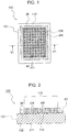
- Fig. 1 is a plan view that conceptually indicates the structure of a transparent electrode member according to an embodiment of the present invention.
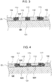
- Fig. 2 is a cross-sectional view taken along line V1-V1 in Fig. 1 .
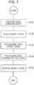
- Fig. 3 is a partial cross-sectional view that conceptually indicates an example of the specific structure of a transparent electrode of the transparent electrode member according to an embodiment of the present invention.
- Fig. 4 is a partial cross-sectional view that conceptually indicates another example of the specific structure of the transparent electrode of the transparent electrode member according to an embodiment of the present invention.
- the transparent electrode member 100 includes a base material 101 having a translucent property.
- “transparency” and “translucent property” indicate a state in which visible light transmittance is 50% or higher (preferably, 80% or higher). Furthermore, it is preferable for the haze value to be 6% or lower.
- “light shielding” and “light shielding property” indicate a state in which visible light transmittance is lower than 50% (preferably, lower than 20%).
- the base material 101 is formed from a glass base material or a transparent base material, such as polyethylene terephthalate (PET), in a film shape.
- PET polyethylene terephthalate
- the transparent electrode member 100 has a transparent electrode 110 having a translucent property and an insulating layer 102, which are placed on a first surface S1, which is one surface of the base material 101.
- the insulating layer 102 is placed in an insulating region IR positioned in at least part of the circumference of a region in which the transparent electrode 110 is placed, when viewed from the direction of the normal to the first surface S1.
- the transparent electrode 110 has a dispersion layer DL that includes a matrix MX composed of an insulating material and also includes conductive nanowires NW in the matrix MX, as indicated in Fig. 3 and Fig. 4 .
- the insulating material forming the matrix MX include a polyester resin, an acrylic resin, a polyurethane resin, and the like.
- the conductive nanowire NW at least one selected from a group comprising a gold nanowire, a silver nanowire, and a copper nanowire is used. The dispersibility of the conductive nanowires NW is assured by the matrix MX. Since at least some of a plurality of conductive nanowires NW come into contact with one another, the conductivity of the transparent electrode 110 in its plane is maintained.
- the transparent electrode 110 has a region (conductive region) CR composed of a conductive part 111 as well as regions (optical adjustment regions) AR having optical adjustment parts 112 when viewed from the direction of the normal to the first surface S1, as indicated in Fig. 1 and Fig. 2 .
- the conductivity of the conductive part 111 is higher than the conductivity of the optical adjustment part 112.
- the dispersion density of conductive nanowires NW in the optical adjustment part 112 is lower than in the conductive part 111.
- conductive nanowires NW are dispersed in the matrix MX and are mutually linked in the dispersion layer DL that the transparent electrode 110 has, high conductivity can be attained when compared with other transparent electrode materials, particularly oxide-based conductive materials.
- the conductive nanowire NW itself has no translucent property, a high dispersion density of the conductive nanowires NW in the dispersion layer DL causes the reflectance of the transparent electrode 110 to tend to become high. That is, since, in the transparent electrode 110 having the dispersion layer DL, the dispersion density of the conductive nanowires NW affects both conductivity and reflectance, there is a tradeoff between increasing conductivity and lowering reflectance.
- the transparent electrode 110 is structured so as to have the conductive region CR the conductivity of which is relatively high and also have the optical adjustment region AR the reflectance of which is relatively low, it is achieved to reduce the reflectance of the transparent electrode 110 and increase its invisibility while the conductivity of the transparent electrode 110 is maintained.
- the reflectance of the optical adjustment region AR can be made lower than the reflectance of the conductive region CR without a large difference in optical properties (such as a refractive index) other than the reflectance when compared with a case in which the transparent electrode has through-holes as described in PTL 1 and PTL 2. Therefore, when, for example, there is an image visually recognized through the transparent electrode member 100, the evenness of the display of the image can be enhanced. Furthermore, when the structure of the optical adjustment region AR is appropriately controlled, it is also possible to increase the conductivity of the optical adjustment region AR when compared with the through-holes provided in the transparent electrode 110.
- the reflectance of the insulating region IR it is preferable for the reflectance of the insulating region IR to be lower than the reflectance of the conductive region CR.
- the difference in reflectance between the insulating region IR and the transparent electrode 110, the reflectance of which has been lowered as a whole by providing the optical adjustment regions AR becomes lower than a case in which no optical adjustment part 112 is provided. Therefore, it becomes difficult to visually recognize the boundary between the transparent electrode 110 and the insulating region IR, so the invisibility of the transparent electrode 110 can be enhanced.
- the insulating layer 102 placed in the insulating region IR to include the matrix MX, which is one of the constituent elements of the dispersion layer DL.
- the matrix MX which is one of the constituent elements of the dispersion layer DL.
- the dispersion density of conductive nanowires NW may be lowered to an extent in which an insulation property is exhibited.
- Fig. 3 is a specific example of this structure (first structure).
- the dispersion layer DL is composed of the matrix MX.
- conductive nanowires NW which are a material that increases reflectance, are not essentially present, the reflectance of the optical adjustment part 112 is particularly lowered.
- Fig. 3 is a specific example of this structure (first structure).
- the insulating layer 102 placed in the insulating region IR in the transparent electrode member 100 is composed of the matrix MX as in the dispersion layer DL of the optical adjustment part 112.
- the structure of the transparent electrode member 100 is such that members placed in regions (insulating region IR and optical adjustment regions AR) positioned around the conductive region CR, the reflectance of the regions being low, are composed of a common material (matrix MX).
- the transparent electrode member 100 has this structure, the reflectance of the whole of the transparent electrode 110 is particularly low and the invisibility of the transparent electrode 110 is more stably improved.
- both the insulating layer 102 and the optical adjustment part 112 are composed of the matrix MX without the conductive nanowires NW essentially being present, this is not a limitation. If conductivity of both the insulating layer 102 and optical adjustment part 112 is appropriately lowered and they become non-conductive and can bring out an insulation function, conductive nanowires NW or materials based on the conductive nanowire NW may be still dispersed in the matrix MX.
- the visibility of the optical adjustment part 112 can be appropriately lowered. Furthermore, although conductivity is lower than in the dispersion layer DL of the conductive part 111, a certain degree of conductivity can be assured due to the conductive nanowires NW positioned on the side close to the base material 101. Therefore, if the dispersion layer DL of the optical adjustment part 112 has the structure indicated in Fig. 4 , the conductivity of the whole of the transparent electrode 110 can be increased.
- the optical adjustment regions AR are positioned in the conductive region CR as indicated in Fig. 1 .
- the conductive region CR In the case of this structure, there is no portion in which the optical adjustment region AR comes into direct contact with the insulating region IR. Therefore, it becomes possible to use the conductive region CR to appropriately form conductive paths in the transparent electrode 110, suppressing a drop in the conductivity of the transparent electrode 110. If there is a portion in which the optical adjustment region AR comes into direct contact with the insulating region IR, the conductive path formed in the transparent electrode 110 may meander. In this case, the conductivity of the transparent electrode 110 is lowered. Also, due to having a portion in which the optical adjustment region AR is connected to the insulating region IR, invisibility may be lowered as will be described later.
- the area ratio (adjustment ratio) of the optical adjustment regions AR is not limited. It is sometimes preferable for the adjustment ratio to be 40% or less as will be described later. With the optical adjustment part 112, conductivity tends to be relatively lowered as a tradeoff for lowering reflectance. With the transparent electrode member 100 according to an embodiment of the present invention, however, even if the adjustment ratio is increased to about 40% to improve the invisibility of the transparent electrode 110, there is a case in which conductivity demanded for the transparent electrode 110 can be assured.
- the optical adjustment regions AR have a plurality of partial regions that are discretely positioned in the conductive region CR. If the optical adjustment region AR and conductive region CR that have relatively different translucent properties form a large pattern separately, it is feared that the visibility of the pattern is increased depending on the shape of the pattern. Also, since the optical adjustment part 112 is a region with relatively low conductivity, if a collection of optical adjustment parts 112 is positioned in the transparent electrode 110, conductive paths meandering in the transparent electrode 110 may be formed. In this case, the conductivity of the transparent electrode 110 is lowered.
- optical adjustment regions AR optical adjustment regions
- a pattern that is likely to be visually recognized is formed in the transparent electrode 110 and conductively is essentially lowered.
- the visibility of the insulating region IR may be increased due to the difference of the reflectance of the insulating region IR positioned between the plurality of transparent electrodes 110 from the reflectance of the conductive part 111 in the transparent electrode 110.
- optical adjustment regions AR are discretely placed in the conductive region CR of the transparent electrode 110, it is possible to improve the invisibility of the transparent electrode 110 placed in a state in which at least part of the transparent electrode 110 is enclosed by the insulating region.
- this separation distance sd is the width of the conductive region CR positioned between optical adjustment parts 112 that are discretely placed, so the separation distance sd is the width of an individual conductive path in the transparent electrode 110. Therefore, when the separation distance sd is 30 ⁇ m or more, a drop in the conductivity of the transparent electrode 110 is stably suppressed.
- the shape of each of a plurality of partial regions may be a circle.
- the diameter of the circle may be 10 ⁇ m or more and 100 ⁇ m or less. From the viewpoint of stably improving the invisibility of the transparent electrode 110, it is preferable that the shapes of the plurality of partial regions (optical adjustment regions AR) described above be uniform in the transparent electrode 110. If the shape of this partial region (optical adjustment region AR) is a circle and its diameter is within the above range, it can be easily achieved to set the separation distance between the plurality of partial regions (optical adjustment regions AR) to 30 ⁇ m or more with the adjustment ratio being 40% or less.
- each of the plurality of partial regions may be a quadrangle instead of a circle.
- the length of the longest diagonal line of the diagonal lines of the quadrangle be 10 ⁇ m or more and 100 ⁇ m or less due to a reason similar to the above reason.
- the plurality of partial regions are placed across the transparent electrode 110, as indicated in Fig. 1 , variations are less likely to occur in reflectance in the whole of the transparent electrode 110, so the invisibility of the transparent electrode 110 is likely to be improved, which is preferable.
- Fig. 5 is a plan view that conceptually indicates the structure of an example of a transparent electrode member having a plurality of transparent electrodes.
- a transparent electrode member 200 according to an embodiment of the present invention has a plurality of transparent electrodes, 110a to 110d. Since insulating regions IR are positioned in at least part of the circumferential region around these transparent electrodes 110a to 110d, the transparent electrode 110a and transparent electrode 110b are electrically independent from each other and the transparent electrode 110c and transparent electrode 110d are electrically independent from each other.
- insulating regions IR are positioned between the transparent electrode 110a and transparent electrode 110b and the transparent electrode 110c, and insulating regions IR are also positioned between the transparent electrode 110a and transparent electrode 110b and the transparent electrode 110d.
- a transparent wire 130 composed of a material having a translucent property is positioned between the transparent electrode 110a and the transparent electrode 110b, electrically connecting the transparent electrode 110a and transparent electrode 110b together.
- the transparent wire 130 is formed from the dispersion layer DL as with the transparent electrode 110a and transparent electrode 110b, and has the conductive region CR and optical adjustment regions AR.
- a region composed of the transparent electrodes 110a to 110d and a region composed of insulating regions IR and the transparent wire 130 are present on the first surface S1. Even in this case, since the translucent property of the transparent electrode 110 is appropriately enhanced, patterns based on these regions are less likely to be visually recognized. Incidentally, even if no optical adjustment region AR is provided in the transparent wire 130 as indicated in Fig. 5 , if the area of the transparent wire 130 is appropriately small, an influence on visibility can be lowered.
- the length (width) of the transparent wire 130 in the minor-axis direction prefferably has been set so as to be smaller than the lengths of the transparent electrodes (transparent electrode 110a and transparent electrode 110b) connected to the transparent wire 130 in that direction.
- the non-adjustment region NR may be provided in the region around the transparent wire 130.
- the conductivity of the optical adjustment part 112 is relatively lowered, charges tend to concentrate in the region around the transparent wire 130 during usage. Due to this, by providing the non-adjustment region NR, it is possible to lower the possibility of the occurrence of a problem such as the blowout of the conductive nanowire NW due to charge concentration.
- An example of the method, according to an embodiment of the present invention, of manufacturing a transparent electrode member is a method of manufacturing the transparent electrode member 100 in the first structure described above.
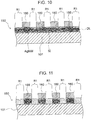
- Fig. 7 is a flowchart of the method of manufacturing the transparent electrode member in the first structure.
- Fig. 8 is a cross-sectional view that conceptually indicates a state in which a first laminated body is prepared.
- Fig. 9 is a cross-sectional view that conceptually indicates a state in which a resist layer is placed on the first laminated body.
- Fig. 10 is a cross-sectional view that conceptually indicates a state in which processing based on an iodine liquid has been performed.
- Fig. 11 is a cross-sectional view that conceptually indicates a state in which processing based on a thiosulfate solution has been performed.
- Fig. 12 is a cross-sectional view that conceptually indicates a state in which the resist layer has been removed.
- a first laminated body 150 is prepared in which a layer in which silver nanowires AgNW, which are one type of conductive nanowires NW, are dispersed in the matrix MX is laminated on the first surface S1 of the base material 101 as the dispersion layer DL as indicated in Fig. 8 (S101).
- the dispersion density of the silver nanowires AgNW in this dispersion layer DL is equal to the dispersion density of the silver nanowires AgNW in the conductive part 111 of the transparent electrode member 100 that is finally obtained.
- a resist layer 160 (S102).
- a positive-type or negative-type photoresist or a film resist is formed on the dispersion layer DL.
- the photoresist is formed by one of various methods such as a roll coat method so that the film thickness becomes about 1 ⁇ m to 5 ⁇ m.
- a film resist When a film resist is used, a film resist with a film thickness of about 20 ⁇ m is used.
- the photoresist is partially exposed by using a mask and an exposure machine. By developing a conductive layer exposed in a subsequent development process by using an alkaline liquid such as TMAH, the resist layer 160 partially remains as indicated in Fig. 9 .
- a first region R1 which is not covered by the resist layer 160, in the dispersion layer DL is processed with an iodine liquid (S103). Due to this processing, at least part of silver nanowires AgNW present in the first region R1 is iodinated to a silver iodide SI as indicated in Fig. 10 , making the dispersion layer DL positioned in the first region R1 insulative.
- the solution infiltrates into the interior of the dispersion layer DL in regions that are not covered by the resist layer 160 and at least part of the silver nanowires AgNW is iodinated and is transformed to a silver iodide SI.
- the area resistivity of the dispersion layer DL in that region is increased, resulting in a state in which an insulation function that is essentially electrical can be brought out.
- silver nanowires AgNW in the dispersion layer DL are iodinated in the first region R1, and whitish or white metallic compounds (including a silver iodide SI) is created.
- the first region R1 is processed with a thiosulfate solution (S104). Due to this processing, at least part of the silver iodide SI is removed from the first region R1 as indicated in Fig. 11 .
- a thiosulfate solution a sodium thiosulfate solution with a concentration of 1.0 to 25 mass% is used.
- the silver iodide SI may return to sliver. If the silver iodide SI returns to silver like this, the reflectance of the optical adjustment part 112 becomes equivalent to the reflectance of the conductive part 111, and the optical adjustment function of the optical adjustment region AR in which the optical adjustment part 112 is positioned is lowered. Furthermore, if silver nanowires AgNW become whitish or white during iodination, contrast to the silver nanowires AgNW makes the obtained silver iodide SI noticeable. Therefore, it is preferable to perform processing as described above to remove metallic compounds, such as a silver iodide SI, positioned on the front surface side of the dispersion layer DL positioned in the first region R1.
- the resist layer 160 is removed by using a resist stripping liquid (S105).
- the transparent electrode member 100 that has the insulative optical adjustment parts 112 and insulating layer 102 in the first region R1 and also has the conductive part 111 in the region that has been covered by the resist layer 160, as indicated in Fig. 12 .
- the insulating layer 102 and optical adjustment parts 112 can be manufactured by one-time resist working. Therefore, the transparent electrode member 100 can be efficiently manufactured. Also, in the transparent electrode member 100 in the first structure, the optical properties of the insulating layer 102 and optical adjustment part 112 become equal. Due to this, patterns formed by the transparent electrode 110 and insulating regions IR become less likely to be visually recognized. Therefore, the transparent electrode member 100 with particularly high invisibility may be obtained when the transparent electrode member 100 is manufactured by the manufacturing method described above.
- Fig. 36(a) is a drawing that indicates a state in which processing based on a thiosulfate solution has been performed in a variation of the method of manufacturing the transparent electrode member in the first structure.
- Fig. 36(b) is a cross-sectional view that conceptually indicates a state in which a transparent electrode member has been obtained by removing a first resist layer.
- S104 thiosulfate solution processing
- S103 iodine liquid processing
- the optical adjustment part 112 and conductive part 111 become more difficult to visually identify. Therefore, the invisibility of the transparent electrode member 100 is improved. If a manufacturing method similar to that for the optical adjustment part 112 is executed for the insulating layer 102 to form a similar structure, this is preferable in that the manufacturing process is simplified. This is also preferable in that the insulating layer 102 is less likely to be visually recognized from the conductive part 111 (invisibility is improved).
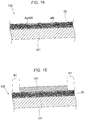
- the first laminated body 150 is prepared in which a layer in which silver nanowires AgNW, which are one type of conductive nanowires NW, are dispersed in the matrix MX is laminated on the first surface S1 of the base material 101 as the dispersion layer DL, as indicated in Fig. 14 (S201).
- the dispersion density of the silver nanowires AgNW in this DL is equal to the dispersion density of the silver nanowires AgNW in the conductive part 111 of the transparent electrode member 100 that is finally obtained.
- first resist layer 161 As indicated in Fig. 15 (S202). Details of the first resist layer 161 and a second resist layer 162, which will be described later, are common to the resist layer 160, so descriptions will be omitted.
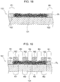
- the first region R1 which is not covered by the first resist layer 161, in the dispersion layer DL is processed with an iodine liquid (S203). Details of this processing are similar to the case of the method of manufacturing the transparent electrode member 100 in the first structure, so descriptions will be omitted. Due to this processing, at least part of silver nanowires AgNW present in the first region R1 is iodinated to a silver iodide SI as indicated in Fig. 16 , making the dispersion layer DL positioned in the first region R1 insulative.
- the first region R1 is processed with a thiosulfate solution (S204). Details of this processing are similar to the case of the method of manufacturing the transparent electrode member 100 in the first structure, so descriptions will be omitted. Due to this processing, at least part of the silver iodide SI is removed from the first region R1 as indicated in Fig. 17 . As a result, the translucent property of the dispersion layer DL positioned in the first region R1 is enhanced.
- the first resist layer 161 is removed by using a resist stripping liquid (S205). As a result, an intermediate member 151 that has the insulating layer 102 in the first region R1 is obtained.
- the transparent electrode member 100 is manufactured as the starting member of this intermediate member 151.
- a second region R2 which is part of the region that has been covered by the first resist layer 161 in the dispersion layer DL, is covered by the second resist layer 162, as indicated in Fig. 19 (S206).
- an iodine liquid S207.
- silver nanowires AgNW have been appropriately removed from the dispersion layer DL positioned in this region, so this processing based on the iodine liquid does not affect the first region R1. Due to this processing, at least part of silver nanowires AgNW present in the third region R3 is iodinated to a silver iodide SI as indicated in Fig. 20 so that the conductivity of the third region R3 falls below the conductivity of the second region R2.
- the third region R3 is processed with a thiosulfate solution (S208). Due to this processing, at least part of the silver iodide SI is removed from the third region R3 as indicated in Fig. 21 . As a result, the translucent property of the dispersion layer DL positioned in the third region R3 is enhanced.
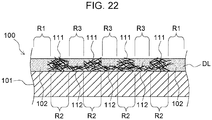
- the transparent electrode member 100 is obtained in which the insulating layer 102 is provided in the first region R1, the conductive part 111 is provided in the second region R2, and the optical adjustment part 112 with conductivity higher than the conductivity of the insulating layer 102 and lower than the conductivity of the conductive part 111 is provided in the third region R3, as indicated in Fig. 22 .
- the optical adjustment part 112 with a certain level of conductivity can be manufactured. Therefore, the transparent electrode member 100 having the transparent electrode 110 with high conductivity can be manufactured. Also, when the manufacturing method described above is appropriately executed, silver nanowires AgNW present at a distance from the base material 101 in the dispersion layer DL can be preferentially removed. Since the silver nanowire AgNW in this portion in the dispersion layer DL the most affects visibility, it is also possible to form the optical adjustment part 112 with low reflectance and high conductivity. When the optical adjustment part 112 of this type is formed, the transparent electrode member 100 with higher conductivity and higher invisibility may be obtained.
- the insulating layer 102 and optical adjustment part 112 a structure in which metallic compounds such as a silver iodide SI are removed on the front surface side (on the side distant from the base material 101) so that the insulating layer 102 and optical adjustment part 112 are essentially composed of the matrix MX and metallic compounds such as a silver iodide SI are dispersed in the matrix MX on the lower layer side of the front surface side (on the side close to the base material 101), as indicated in Fig. 37 and Fig. 38 .
- FIG. 37(a) is a drawing that indicates a state in which processing based on a thiosulfate solution has been performed to form an insulating layer in a variation of the method of manufacturing the transparent electrode member in the second structure.
- Fig. 37(b) is a cross-sectional view that conceptually indicates a state in which an intermediate member has been obtained by removing the first resist layer.
- Fig. 38(a) is a drawing that indicates a state in which processing based on a thiosulfate solution has been performed to form the optical adjustment part in a variation of the method of manufacturing the transparent electrode member in the second structure.
- Fig. 38(b) is a cross-sectional view that conceptually indicates a state in which a transparent electrode member has been obtained by removing the second resist layer.
- this intermediate member 151 has the insulating layer 102 in which a region composed of the matrix MX is positioned on the front surface side and a region in which metallic compounds such as a silver iodide SI are dispersed is positioned on the lower layer side of the region composed of the matrix MX (on the side close to the base material 101).
- step S206 is performed for this intermediate member 151 and iodine liquid processing to form the optical adjustment part 112 (S207) is further performed, by, for example, shortening time in processing based on a thiosulfate solution (S208), only metallic compounds, on the front surface side, that are part of the metallic compounds such as a silver iodide SI (see Fig. 20 ) positioned in the third region R3, are removed as indicated in Fig. 38(a) .
- the optical adjustment part 112 as indicated in Fig. 38(b) is obtained instead of Fig.
- a region composed of the matrix MX is positioned on the front surface side, a region in which metallic compounds such as a silver iodide SI are dispersed is positioned on the lower layer side of the region composed of the matrix MX (on the side close to the base material 101), and a region in which silver nanowires AgNW are dispersed is further positioned on the lower layer side of the region with metallic compounds dispersed.
- the transparent electrode member 100 has a structure like this, the insulating layer 102, optical adjustment part 112, and conductive part 111 become particularly difficult to visually identify. Therefore, the invisibility of the transparent electrode member 100 is further improved.
- the above transparent electrode member 100 according to an embodiment of the present invention can be preferably used as a constituent element of a position sensor such as a capacitive sensor.
- a capacitive sensor having the transparent electrode member 100 will be described below.
- Fig. 23 is a plan view that represents a capacitive sensor according to this embodiment.
- Fig. 24 is a plan view in which the region A1 represented in Fig. 23 is enlarged.
- Fig. 25 is a cross-sectional view in cross-section C1-C1 represented in Fig. 24 .
- Fig. 26 is a cross-sectional view in cross-section C2-C2 represented in Fig. 24 .
- transparent electrodes are transparent, they cannot be originally viewed. In Fig. 23 and Fig. 24 , however, the outlines of the transparent electrodes are indicated for easy understanding.
- a capacitive sensor 1 has a base material 2, first transparent electrodes 4, second transparent electrodes 5, bridge wiring parts 10, and a panel 3 as well as a detection unit and a control unit (which are not illustrated).
- the panel 3 is provided on the opposite side to the base material 2 when viewed from the bridge wiring part 10.
- An optical clear adhesive (OCA) 30 is provided between the base material 2 and the panel 3.
- An insulating part 20 is provided between the base material 2 and the bridge wiring part 10.
- the optical clear adhesive 30 is provided between the bridge wiring part 10 and the panel 3.
- the base material 2 is formed from a glass base material or a transparent base material such as polyethylene terephthalate (PET), which has a translucent property, in a film shape.
- the first transparent electrodes 4 and second transparent electrodes 5 are provided on a main surface 2a, which is one of the main surfaces of the base material 2. Details of this will be described below.
- the panel 3 is provided on the opposite side to the base material 2 when viewed from the bridge wiring part 10 and has a translucent property. When a manipulating body such as a finger of the manipulator comes into contact with or close to this panel 3, a manipulation to transparent electrodes is performed.
- the material of the panel 3 is not particularly restricted.
- the panel 3 is bonded to the base material 2 through the optical clear adhesive 30 provided between the base material 2 and the panel 3.
- the optical clear adhesive 30 is composed of an acrylic adhesive, a double-sided adhesive tape, or the like.
- the capacitive sensor 1 is composed of a detection region 11 and a non-detection region 25 when viewed from a direction (Z1-Z2 direction: see Fig. 25 and Fig. 26 ) along the normal to a surface on the same side as the panel 3.
- the detection region 11 is a region on which a manipulation can be performed with a manipulating body such as a finger
- the non-detection region 25 is a region, shaped like a picture frame, that is positioned on the outer circumference side of the detection region 11.
- the non-detection region 25 is light-shielded by a decorative layer, which is not illustrated.
- the capacitive sensor 1 In the capacitive sensor 1, light (exemplified by external light) from a surface on the same side as the panel 3 toward a surface on the same side as the base material 2 and light (exemplified by light from a backlight of a display device used in combination with the capacitive sensor 1) from the surface on the same side as the base material 2 toward the surface on the same side as the panel 3 are less likely to pass through the non-detection region 25.
- first electrode links 8 and second electrode links 12 are provided on the main surface 2a, which is one of the main surfaces of the base material 2.
- the first electrode link 8 is placed in the detection region 11 and has a plurality of first transparent electrodes 4.
- the plurality of first transparent electrodes 4 are provided on the main surface (sometimes simply referred to below as the "front surface") 2a, which is one of the main surfaces of the base material 2 and is positioned on the Z1 side, the normal to the main surfaces being along the Z1-Z2 direction.
- Each first transparent electrode 4 is linked through an elongated link 7 in the Y1-Y2 direction (first direction).
- the link 7 is formed integrally with the first transparent electrode 4.
- the link 7 electrically connects two adjacent first transparent electrodes 4 to each other.
- the insulating region IR is provided around the first electrode links 8 and second electrode links 12.
- the first transparent electrode 4 and link 7 are formed from a material that has a translucent property and includes conductive nanowires.
- a material including conductive nanowires it is possible to achieve a high translucent property and low electric resistance for the first transparent electrode 4. Also, by using a material including conductive nanowires, it is possible to improve the deformation performance of the capacitive sensor 1.
- the first transparent electrode 4 has a plurality of first optical adjustment regions 41.
- the plurality of first optical adjustment regions 41 are placed apart from one another and are provided across the whole of the first transparent electrode 4.
- the distance (first distance) D1 between adjacent first optical adjustment regions 41 is constant; the distance is 30 ⁇ m or more. That is, the plurality of first optical adjustment regions 41 are evenly provided across the whole of the first transparent electrode 4.
- the shape of the first optical adjustment region 41 is a circle.
- the diameter D11 of the first optical adjustment region 41 is 10 ⁇ m or more and 100 ⁇ m or less. Details of dimensions related to the first optical adjustment region 41 will be described later.
- the second electrode link 12 is placed in the detection region 11 and has a plurality of second transparent electrodes 5.
- the plurality of second transparent electrodes 5 are provided on the front surface 2a of the base material 2.
- the second transparent electrodes 5 are provided on the same surface (front surface 2a of the base material 2) as the first transparent electrodes 4.
- Each second transparent electrode 5 is linked through the elongated bridge wiring part 10 in the X1-X2 direction (second direction).
- the second electrode links 12, each of which has the plurality of second transparent electrodes 5 linked in the X1-X2 direction are arranged in the Y1-Y2 direction at intervals.
- the bridge wiring part 10 is formed as a body separate from the second transparent electrodes 5.
- the X1-X2 direction crosses the Y1-Y2 direction.
- the X1-X2 direction perpendicularly crosses the Y1-Y2 direction.
- the second transparent electrode 5 is formed from a material that has a translucent property and includes conductive nanowires.
- the conductive nanowires are as described above in relation to the material of the first transparent electrode 4.
- the second transparent electrode 5 has a plurality of second optical adjustment regions 51.
- the plurality of second optical adjustment regions 51 are placed apart from one another and are provided across the whole of the second transparent electrode 5.
- the distance (second distance) D2 between adjacent second optical adjustment regions 51 is constant; the distance is 30 ⁇ m or more. That is, the plurality of second optical adjustment regions 51 are evenly provided across the whole of the second transparent electrode 5.
- the shape of the second optical adjustment region 51 is a circle.
- the diameter D12 of the second optical adjustment region 51 is 10 ⁇ m or more and 100 ⁇ m or less. Details of dimensions related to the second optical adjustment region 51 will be described later together with dimensions related to the first optical adjustment region 41.
- the bridge wiring part 10 is formed from a material that has a translucent property and conductivity and includes an oxide material.
- an oxide material As the oxide material that has a translucent property and conductivity, at least one selected from a group of ITO (Indium Tin Oxide), IZO (Indium Zinc Oxide), GZO (Gallium-doped Zinc Oxide), AZO (Aluminum-doped Zinc Oxide), and FTO (Fluorine-doped Tin Oxide) is used.
- the bridge wiring part 10 may have a first layer including an oxide material such as ITO and a second layer composed of a metal that has a lower resistance than the first layer and is transparent. Also, the bridge wiring part 10 may further have a third layer including an oxide material such as ITO. If the bridge wiring part 10 has a laminated structure of the first layer and second layer or a laminated structure of the first layer, second layer, and third layer, it is preferable that there be etching selectivity between the bridge wiring part 10 and the first transparent electrode 4 and second transparent electrode 5.
- the insulating part 20 is provided on the front surface of the link 7, which links individual first transparent electrodes 4. As indicated in Fig. 25 , the insulating part 20 fills space between the link 7 and the second transparent electrode 5 and also slightly rides on the front surface of the second transparent electrode 5. As the insulating part 20, a novolak resin (resist), for example, is used.
- the bridge wiring part 10 is provided from the front surface 20a of the insulating part 20 to the front surfaces of the individual second transparent electrodes 5 positioned on both sides of the insulating part 20 in the X1-X2 direction.
- the bridge wiring part 10 electrically connects two adjacent second transparent electrodes 5 to each other.
- the insulating part 20 is provided on the front surface of the link 7, which links individual first transparent electrodes 4, and the bridge wiring part 10, which connects individual second transparent electrode 5, is provided on the front surface of the insulating part 20.
- the insulating part 20 intervenes between the link 7 and the second linking part 10 and the first transparent electrode 4 and second transparent electrode 5 are in a state in which they are electrically insulated from each other. Since, in this embodiment, the first transparent electrode 4 and second transparent electrode 5 are provided on the same surface (front surface 2a of the base material 2), the thinning of the capacitive sensor 1 can be achieved.
- the first transparent electrode 4 and second transparent electrode 5 are arranged adjacently on the main surface 2a of the base material 2.
- the first transparent electrode 4 and second transparent electrode 5 correspond to the transparent electrodes, 110a to 110d in Fig. 5 and Fig. 6 .
- An insulating layer 21 is provided between the first transparent electrode 4 and the second transparent electrode 5.
- the insulating layer 21 corresponds to the insulating region IR in Fig. 5 , Fig. 6 , and Fig. 23 . Due to this, the first transparent electrode 4 and second transparent electrode 5 are placed in a state in which they are electrically insulated from each other.
- the insulating layer 21 may be embedded in, for example, a novolak resin (resist) or the like by an insulating material. That is, an insulating material may intervene in the insulating layer 21 between the first transparent electrode 4 and the second transparent electrode 5. As described above, the insulating part 20 intervenes in part of the insulating layer 21 (between the second transparent electrode 5 and the link 7 of the first transparent electrode 4). That is, the first transparent electrode 4 and second transparent electrode 5 are placed in a state in which they are segmented from each other through the insulating part 20 and part of the insulating layer 21.
- the width D3 of the insulating layer 21 is, for example, about 10 ⁇ m or more and 20 ⁇ m or less. Details of the width D3 of the insulating layer 21 will be described later.
- the link 7 represented in Fig. 24 to Fig. 26 is integrally formed as part of the first transparent electrode 4 and extends in the Y1-Y2 direction.
- the bridge wiring part 10 represented in Fig. 24 to Fig. 26 is formed on the front surface 20a of the insulating part 20, which covers the link 7, as a body separate from the second transparent electrodes 5 and extends in the X1-X2 direction.
- forms of the placement of the link 7 and bridge wiring part 10 are not limited to this.
- the link 7 may be integrally formed as part of the second transparent electrode 5 and may extend in the X1-X2 direction. In this case, the link 7 electrically connects two adjacent second transparent electrodes 5 to each other.
- the bridge wiring part 10 may be formed on the front surface 20a of the insulating part 20, which covers the link 7, as a body separate from the first transparent electrodes 4, and may extend in the Y1-Y2 direction. In this case, the bridge wiring part 10 electrically connects two adjacent first transparent electrodes 4 to each other.
- the bridge wiring part 10 is formed on the front surface 20a of the insulating part 20, which covers the link 7, as a body separate from the second transparent electrodes 5, and extends in the X1-X2 direction.
- a plurality of wiring parts 6 led out from individual first electrode links 8 and individual second electrode links 12 are formed in the non-detection region 25.
- Each of the first electrode links 8 and second electrode links 12 is electrically connected to the wiring part 6 through a connection wire 16.
- Each wiring part 6 is connected to an external connection part 27 that is electrically connected to a flexible printed circuit board, which is not illustrated. That is, each wiring part 6 electrically connects the first electrode link 8 and second electrode link 12 and the external connection part 27.
- the external connection part 27 is electrically connected to the flexible printed circuit board, which is not illustrated, through, for example, a material that has a conductive paste or a metal such as Cu, a Cu alloy, a CuNi alloy, Ni, Ag, Au, or the like.
- the detection unit that detects a change in capacitance generated between the manipulating body and a transparent electrode (mainly, the first transparent electrode 4 or second transparent electrode 5) and the control unit that calculates the position of the manipulating body according to a signal from the detection unit are mounted.
- a transparent electrode mainly, the first transparent electrode 4 or second transparent electrode 5
- the control unit that calculates the position of the manipulating body according to a signal from the detection unit.
- an integrated circuit is used in the detection unit and control unit.
- Each wiring part 6 is formed from a material that has a metal such as Cu, a Cu alloy, a CuNi alloy, Ni, Ag, Au, or the like.
- the connection wire 16 is formed from a transparent conductive material such as ITO or metal nanowires and extends from the detection region 11 to the non-detection region 25.
- the wiring part 6 is laminated on the connection wire 16 in the non-detection region 25 and is electrically connected to the connection wire 16.
- the capacitive sensor 1 may have a laminated wiring structure in which the dispersion layer DL having the same metal nanowires (a specific example is silver nanowires) as the first transparent electrode 4 and second transparent electrode 5 continuously extends to the non-detection region 25 to form the connection wire 16 and, in the non-detection region 25, this connection wire 16 and a metal layer forming the wiring part 6 are laminated.
- the dispersion layer DL having the same metal nanowires (a specific example is silver nanowires) as the first transparent electrode 4 and second transparent electrode 5 continuously extends to the non-detection region 25 to form the connection wire 16 and, in the non-detection region 25, this connection wire 16 and a metal layer forming the wiring part 6 are laminated.
- the wiring part 6 is provided at a portion, on the front surface 2a of the base material 2, where the non-detection region 25 is positioned.
- the external connection part 27 is also provided at a portion, on the front surface 2a of the base material 2, where the non-detection region 25 is positioned, as is the wiring part 6.
- the wiring part 6 and external connection part 27 are illustrated so as to be visually recognized for easy understanding.
- a decorative layer (not illustrated) having a shielding property is provided at a portion where the non-detection region 25 is positioned. Therefore, the wiring part 6 and external connection part 27 are hidden by the decorative layer and are not visually recognized when the capacitive sensor 1 is viewed from the panel on the same side as the panel 3.
- Any material can be used to form the decorative layer if the material has a light shielding property.
- the decorative layer may have an insulating property.
- the capacitive sensor 1 when a finger, which is an example of a manipulation body, is caused to come into contact with, for example, a surface 3a of the panel 3 as indicated in Fig. 25 , a capacitance is generated between the finger and the first transparent electrode 4 close to the finger and between the finger and the second transparent electrode 5 close to the finger.
- the capacitive sensor 1 can detect a change in capacitance at this time by the detecting unit and can calculate the contact position of the finger by the control unit according to this change in capacitance.
- the capacitive sensor 1 detects the X coordinate of the position of the finger according to a change in capacitance between the finger and the first electrode link 8 and detects the Y coordinate of the position of the finger according to a change in capacitance between the finger and the second electrode link 12 (self-capacitance detection type).
- the capacitive sensor 1 may be of mutual capacitance detection type. That is, the capacitive sensor 1 may apply a driving voltage to one string of electrodes, which is any one of the first electrode link 8 and second electrode link 12, and may detect a change in capacitance between the finger and the other electrode of the first electrode link 8 and the second electrode link 12. Due to this, the capacitive sensor 1 detects the Y coordinate of the position of the finger from the other electrode and detects the X direction of the position of the finger from one electrode.
- the capacitive sensor has a reflection preventing layer, a reflection reducing layer, or the like, the difference between the reflectance of the conductive region and the reflectance of the insulating part can be suppressed, but a facility to form the reflection preventing layer or reflection reducing layer needs to be added and process to manufacture the capacitive sensor are increased.
- the first transparent electrode 4 has a plurality of first optical adjustment regions 41 placed apart from one another.
- the second transparent electrode 5 has a plurality of second optical adjustment regions 51 placed apart from one another. Therefore, in the first transparent electrode 4 and second transparent electrode 5, a conductive region including conductive nanowires and a plurality of regions (optical adjustment regions) formed by a plurality of first optical adjustment regions 41 and a plurality of second optical adjustment regions 51 are present. Therefore, in the first transparent electrode 4 and second transparent electrode 5, a plurality of boundaries (inner boundaries) between the conductive region and the optical adjustment regions are present. On the other hand, a boundary (outer boundary) between the first transparent electrode 4 and the insulating layer 21 and a boundary (outer boundary) between the second transparent electrode and the insulating layer 21 are present.
- the first transparent electrodes 4 and second transparent electrodes 5 become difficult to visually recognize as patterns. Due to this, the pattern invisibility of the first transparent electrodes 4 and second transparent electrodes 5 can be improved.
- the first optical adjustment regions 41 are provided across the whole of the first transparent electrodes 4, and the second optical adjustment regions 51 are provided across the whole of the second transparent electrode 5. According to this, since the first optical adjustment regions 41 and second optical adjustment regions 51 are provided, it is possible to restrain the electric resistances of the first transparent electrode 4 and second transparent electrode 5 from being excessively increased. Also, it is possible to restrain the first optical adjustment regions 41 and second optical adjustment regions 51 from being concentrated and thereby the first transparent electrode 4 and second transparent electrode 5 from being visually recognized easily as a pattern.
- the first distance between adjacent first optical adjustment regions 41 is constant, and the second distance between adjacent second optical adjustment regions 51 is constant. That is, the plurality of first optical adjustment regions 41 are evenly provided across the whole of the first transparent electrode 4. The plurality of second optical adjustment regions 51 are evenly provided across the whole of the second transparent electrode 5. Therefore, it is possible to restrain the electric resistance of each of the first transparent electrode 4 and second transparent electrode 5 from varying depending on the position and to restrain the electric resistances of the first transparent electrode 4 and second transparent electrode 5 from being locally increased. Also, it is possible to restrain the first optical adjustment regions 41 and second optical adjustment regions 51 from being concentrated and thereby the first transparent electrode 4 and second transparent electrode 5 from being visually recognized easily as a pattern.
- the conductive nanowire included in the first transparent electrode 4 and second transparent electrode 5 is at least one selected from a group of a gold nanowire, a silver nanowire, and a copper nanowire. According to this, it is possible to suppress the electric resistance of the first transparent electrode 4 including the first optical adjustment regions 41 and the electric resistance of the second transparent electrode 5 including the second optical adjustment regions 51 to a low resistance when compared with a case in which an oxide material such as, for example, ITO is used as the material of the first transparent electrode 4 and second transparent electrode 5.
- Fig. 27 is a plan view that represents a variation (first variation) of the first transparent electrode and second transparent electrode in this embodiment.
- Fig. 27 is equivalent to a plan view in which the region A1 represented in Fig. 23 is enlarged.
- a first transparent electrode 4A in this variation has a plurality of first optical adjustment regions 41A.
- the shape of the first optical adjustment region 41A is a quadrangle.
- the length D13 of the longest diagonal line of the diagonal lines of the first optical adjustment region 41A in a quadrangular shape is 10 ⁇ m or more and 100 ⁇ m or less. Details of dimensions related to the first optical adjustment region 41A will be described later.
- the other structures of the first transparent electrode 4A are similar to the structure of the first transparent electrode 4 described above in relation to Fig. 23 to Fig. 26 .
- a second transparent electrode 5A in this variation has a plurality of second optical adjustment regions 51A.
- the shape of the second optical adjustment region 51A is a quadrangle.
- the length D14 of the longest diagonal line of the diagonal lines of the second optical adjustment region 51A in a quadrangular shape is 10 ⁇ m or more and 100 ⁇ m or less. Details of dimensions related to the second optical adjustment region 51A will be described later together with dimensions related to the first optical adjustment region 41A.
- the other structures of the second transparent electrode 5A are similar to the structure of the second transparent electrode 5 described above in relation to Fig. 23 to Fig. 26 .
- each of the first optical adjustment region and second optical adjustment region may be a quadrangle without being limited only to a circle.
- the optical properties such as the reflectance of each of the first transparent electrode 4A and second transparent electrode 5A are similar to the optical properties such as the reflectance of each of the first transparent electrode 4 and second transparent electrode 5 described above in relation to Fig. 23 to Fig. 26 . Therefore, even if both inner boundaries and outer boundaries are visually recognized in a plan view of the capacitive sensor 1, it is suppressed that only the outer boundaries are emphasized. Therefore, the first transparent electrodes 4A and second transparent electrodes 5A become difficult to visually recognize as a pattern. Due to this, the pattern invisibility of the first transparent electrodes 4A and second transparent electrodes 5A can be improved.
- Fig. 28 is a graph that exemplifies an example of a relationship between the adjustment ratio and wire resistance.
- the horizontal axis of the graph represented in Fig. 28 represents the adjustment ratio (%).
- the vertical axis of the graph represented in Fig. 28 represents the wire resistance (k ⁇ ).
- adjustment ratio refers to the area of the optical adjustment region per unit area.
- the wire resistance is relatively high.
- the wire resistance in a case in which the screen size is about 4 inches or more and 6 inches or less as with, for example, a movable terminal such as smartphone, to assure the performance of the capacitive sensor 1, it is preferable for the wire resistance to be 20 k ⁇ or less. In Fig. 28 , 20 k ⁇ is indicated by a dashed line. In this case, according to the graph represented in Fig. 28 , it is preferable for the adjustment ratios of the first optical adjustment regions 41 in the first transparent electrode 4 and the second optical adjustment regions 51 in the second transparent electrode 5 to be 40% or less.
- the adjustment ratios of the first optical adjustment regions 41 in the first transparent electrode 4 and the second optical adjustment regions 51 in the second transparent electrode 5 are 40% or less, it is possible to improve the invisibility of the patterns of the first transparent electrodes 4 and second transparent electrodes 5 and suppress the rise of the electric resistance of each of the first transparent electrode 4 and second transparent electrode 5, making it possible to assure the performance of the capacitive sensor 1.
- the screen size of a terminal in which the capacitive sensor 1 according to this embodiment is mounted is about less than 4 inches, to assure the performance of the capacitive sensor 1, it is preferable for wiring resistance to be 30 k ⁇ or less.
- the adjustment ratios of the first optical adjustment regions 41 in the first transparent electrode 4 and the second optical adjustment regions 51 in the second transparent electrode 5 is preferable.
- Fig. 29 is a graph that exemplifies an example of a relationship between a gap width and the adjustment ratio.
- the vertical axis of the graph represented in Fig. 29 represents the gap width ( ⁇ m).
- the horizontal axis of the graph represented in Fig. 29 represents the adjustment ratio (%).
- the gap width represented in Fig. 29 is equivalent to the width D3 of the insulating layer 21 described above in relation to Fig. 24 .
- the present inventor studied the invisibility of the patterns of the first transparent electrodes 4 and second transparent electrodes 5 when the width D3 and adjustment ratio were varied. In this study, the inventor made visual decisions on invisibility. Conditions for visual decisions are as follows.
- a sample was used in which a glass substrate is pasted through an optical transparent adhesive layer to a sensor film on which transparent electrodes having optical adjustment parts are provided.
- a light source that emits light to the sample is a three-waveform type of daylight fluorescent lamp.
- the illumination of the light source is 1300 lux (lx).
- the distance (inspection distance) between the sample and a visual position is 30 cm.
- the angle between the eye line and a straight line (normal) perpendicular to the front surface of the sensor film or glass substrate is 0 degree or more and 45 degrees or less.
- a black board is placed on a side (rear side of the sample) opposite to the eye line.
- FIG. 29 An example of the results of the study is as represented in Fig. 29 . That is, in a case in which the width D3 is 10 ⁇ m, if the adjustment ratio is 15% or more, the invisibility of the patterns of the first transparent electrodes 4 and second transparent electrodes 5 is assured. In a case in which the width D3 is 15 ⁇ m, if the adjustment ratio is 30% or more, the invisibility of the patterns of the first transparent electrodes 4 and second transparent electrodes 5 is assured. In a case in which the width D3 is 20 ⁇ m, if the adjustment ratio is 35% or more, the invisibility of the patterns of the first transparent electrodes 4 and second transparent electrodes 5 is assured. That is, if the width D3 is relatively wide, a relatively high adjustment ratio is needed to assure the invisibility of the patterns of the first transparent electrodes 4 and second transparent electrodes 5.
- the adjustment ratios of the first optical adjustment regions 41 and the second optical adjustment regions 51 it is preferable for the adjustment ratios of the first optical adjustment regions 41 and the second optical adjustment regions 51 to be 40% or less.
- the width D3 it is preferable for the width D3 to be 10 ⁇ m or more and 20 ⁇ m or less in consideration of the invisibility of the patterns of the first transparent electrodes 4 and second transparent electrodes 5 and the allowable limit of the wire resistance. That is, the region A2 represented in Fig. 29 is a region that satisfies both the invisibility of the patterns of the first transparent electrodes 4 and second transparent electrodes 5 and the allowable limit of the wire resistance. As represented in Fig. 29 , it was found that there is a correlation between the invisibility of the patterns of the first transparent electrodes 4 and second transparent electrodes 5 and the adjustment ratios of the first optical adjustment regions 41 and second optical adjustment regions 51.
- Fig. 30 is a graph that exemplifies an example of a relationship between sheet resistance and a continuity assuring line width.
- the horizontal axis of the graph represented in Fig. 30 represents sheet resistance ( ⁇ / ⁇ ).
- the vertical axis of the graph represented in Fig. 30 represents the continuity assuring line width ( ⁇ m).
- the continuity assuring line width refers to the width of an electrical conductor needed to assure its conductivity without the electrical conductor being broken. Therefore, if the sheet resistance is relatively high as represented in Fig. 30 , a relatively long width is needed as the width (continuity assuring line width) of an electrical conductor needed to assure its conductivity without the electrical conductor being broken.
- the upper broken line in the graph represented in Fig. 30 exemplifies a relationship between the sheet resistance and the width of the continuity assuring line width for a transparent electrode formed from a material including silver nanowires.
- the lower limit of the sheet resistance of the transparent electrode formed from a material including silver nanowires is about 30 to 50 ⁇ / ⁇ . Therefore, according to the graph represented in Fig. 30 , for the transparent electrode formed from a material including silver nanowires, it is preferable for the continuity assuring line width to be 30 ⁇ m or more.
- the distance D1 between a plurality of adjacent first optical adjustment regions 41 is 30 ⁇ m or more.
- the second transparent electrode 5 it is preferable for the distance D2 between a plurality of adjacent second optical adjustment regions 51 to be 30 ⁇ m or more.
- first optical adjustment regions 41 are provided in the first transparent electrode 4 including conductive nanowires and a plurality of second optical adjustment regions 51 are provided in the second transparent electrode including conductive nanowires, since the width of the conductive region is narrow, it is possible to restrain the first transparent electrode 4 and second transparent electrode 5 from being broken.
- Fig. 31 is a plan view that explains visibility when optical adjustment parts are provided only in the vicinity of the insulating layer 21 in this embodiment.
- two insulating layers 21, each of which is between the first transparent electrode 4 and the second transparent electrode 5, are indicated so as to be arranged vertically.
- the first transparent electrode 4 is placed between the two insulating layers 21.
- the second transparent electrode 5 is placed on each of both sides of the two insulating layers 21.
- the placement of the transparent electrodes represented in Fig. 30 is placement for convenience of explanation. Therefore, the second transparent electrode 5 may be provided between the two insulating layers 21 and the first transparent electrode 4 may be provided on each of both sides of the two insulating layers 21.
- the width D3 of the insulating layer 21 on the upper side is the same as the width D3 of the insulating layer 21 on the lower side.
- neither the first optical adjustment region 41 nor the second optical adjustment region 51 is provided in the vicinity of the insulating layer 21 on the upper side of the two insulating layers 21 represented in Fig. 31 .
- the first optical adjustment region 41 and second optical adjustment region 51 are provided in the vicinity of the insulating layer 21 on the lower side of the two insulating layers 21 represented in Fig. 31 .
- the insulating layer 21 is emphasized and becomes noticeable due to the existence of the first optical adjustment region 41 and second optical adjustment region 51 when compared with a case in which neither the first optical adjustment region 41 nor the second optical adjustment region 51 is provided in the vicinity of the insulating layer 21.
- the first optical adjustment region 41 and second optical adjustment region 51 which are originally circular, are semicircular and are contiguous to the insulating layer 21 in a stripe shape, a local area due to a region composed of the insulating layer 21, first optical adjustment region 41, and second optical adjustment region 51 is increased.
- first optical adjustment region 41 and second optical adjustment region 51 are provided only in the vicinity of the insulating layer 21 and no optical adjustment region is provided in regions in the transparent electrodes (first transparent electrode 4 and second transparent electrode 5), the regions being distant from the insulating layer 21, as indicated in Fig. 31 . Therefore, it is preferable for the plurality of first optical adjustment regions 41 to be evenly provided across the whole of the first transparent electrode 4 without being concentrated in the vicinity of the insulating layer 21.
- the plurality of second optical adjustment region 51 is evenly provided across the whole of the second transparent electrode 5 without being concentrated in the vicinity of the insulating layer 21.
- optical adjustment regions each of which is a region in which an optical adjustment part is positioned, be positioned in the interior of a conductive region, which is a region in which a conductive part is positioned, and that the optical adjustment region and an insulating region, in which the insulating layer is positioned, are not in direct contact with each other. It is also preferable that the optical adjustment regions be placed across the whole of the transparent electrode.
- Fig. 32 is a graph that exemplifies an example of a relationship between wavelength and reflectance when the diameter of the optical adjustment part is varied.
- Fig. 33 is a graph in which part of the graph represented in Fig. 32 is enlarged.
- Fig. 33 is a graph in which a wavelength range of 500 ⁇ m or more and 600 ⁇ m or less in the graph represented in Fig. 32 is enlarged.
- the present inventor studied a relationship between the wavelength of light and reflectance in a case in which the diameter of the optical adjustment part in a round shape (circular shape) was varied.
- the inventor measured the reflectance of the transparent electrodes by using an ultraviolet-visible (UV-vis) spectrophotometer.
- the measurement method is expanded reflection. Measured waveforms are 250 nm or more and 800 nm or less.
- a sample was used in which a cover member is pasted through an optical transparent adhesive layer to a sensor film on which transparent electrodes having optical adjustment parts are provided.
- the cover member is EAGLE XG (registered trademark), from Corning Incorporated, that has a thickness of 0.5 mm.
- Fig. 32 and Fig. 33 An example of the results of the study is as represented in Fig. 32 and Fig. 33 . That is, when the diameter of the optical adjustment part is relatively large, the reflectance of the transparent electrode is relatively low. From the graphs represented in Fig. 32 and Fig. 33 , it is preferable that the diameter D11 (see Fig. 24 ) of the first optical adjustment region 41 and the diameter D12 (see Fig. 24 ) of the second optical adjustment region 51 be 10 ⁇ m or more, and it is more preferable that these diameters be 20 ⁇ m or more.
- the present inventor obtained, in a case in which the diameter of the optical adjustment part in the transparent electrode is more than 100 ⁇ m, it was visually confirmed that the invisibility of the patterns of the first transparent electrodes 4 and second transparent electrodes 5 is lowered. Conditions for visual confirmation are as described above in relation to Fig. 29 . Due to this, it is preferable that the diameter D11 of the first optical adjustment region 41 and the diameter D12 of the second optical adjustment region 51 be 100 ⁇ m or less, and it is more preferable that these diameters be 90 ⁇ m or less.
- Fig. 34 is a graph that exemplifies an example of a relationship between wavelength and reflectance when the shape of the optical adjustment part is varied.
- Fig. 35 is a graph in which part of the graph represented in Fig. 34 is enlarged.
- Fig. 35 is a graph in which a wavelength range of 500 ⁇ m or more and 600 ⁇ m or less in the graph represented in Fig. 34 is enlarged.
- the present inventor studied a relationship between the wavelength of light and reflectance in a case in which the shape of the optical adjustment part is round (circular) and a case in which the shape is quadrangular.
- the method of measuring reflectance is as described above in relation to Fig. 32 and Fig. 33 .
- Fig. 34 and Fig. 35 An example of the results of the study is as represented in Fig. 34 and Fig. 35 . That is, reflectance in a case in which the shape of the optical adjustment part is round is substantially the same as reflectance in a case in which the shape of the optical adjustment part is quadrangular. Due to this, as described above in relation to Fig. 27 , the shape of each of the first optical adjustment region and second optical adjustment region is not limited to a circle and may be a quadrangle. Like the diameter range described above in relation to Fig. 32 and Fig. 33 , it is preferable that the length D13 (see Fig. 27 ) of the longest diagonal line of the diagonal lines of the first optical adjustment region 41A in a quadrangular shape and the length D14 (see Fig.
- the longest diagonal line of the diagonal lines of the second optical adjustment region 51A in a quadrangular shape be 10 ⁇ m or more, and it is more preferable for these lengths to be 20 ⁇ m or more. Also, it is preferable that the length D13 of the longest diagonal line and the length D14 of the longest diagonal line be 100 ⁇ m or less, and it is more preferable for these lengths to be 90 ⁇ m or less.
- Fig. 39 is a plan view that represents part of a detection region in another variation (second variation) of the capacitive sensor in this embodiment.
- Fig. 39 is a plan view in which the region corresponding to the region A1 represented in Fig. 23 is further enlarged.
- This variation is similar to the example indicated in Fig. 22 in that a first transparent electrode 4B in this variation has a plurality of first optical adjustment regions 41B in a substantially circular shape, a second transparent electrode 5B has a plurality of second optical adjustment regions 51B in a substantially circular shape, and the insulating layer 21 is provided between the first transparent electrode 4B and the second transparent electrode 5B.
- illustration of the insulating part 20 and bridge wiring part 10 is omitted.
- neither the first optical adjustment region 41B nor the second optical adjustment region 51B is provided in a region including the link 7, neither the first optical adjustment region 41B nor the second optical adjustment region 51B is provided. This region is a non-adjustment region NR.
- a dummy region IF which is electrically insulted from both the first transparent electrode 4B and the second transparent electrode 5B by the insulating layers 21, is provided between the first transparent electrode 4B and the second transparent electrode 5B so as to be enclosed by the insulating layers 21.
- the dummy region IF has a dummy conductive region CR1 having a structure in common with the conductive region CR in the first transparent electrode 4B and second transparent electrode 5B, that is, a structure in which conductive nanowires are dispersed in an insulating material that becomes a matrix.
- a plurality of dummy optical adjustment regions AR1 in a substantially circular shape are placed in the dummy conductive region CR1 in the dummy region IF so as to be mutually discrete in a plan view, as in the first optical adjustment region 41B and second optical adjustment region 51B.
- the dummy optical adjustment region AR1 is formed by a method similar to the method for the first optical adjustment region 41B and second optical adjustment region 51B (the method in which conductive nanowires are removed from the insulating material that becomes a matrix at least on the front surface part).
- the dummy optical adjustment region AR1 has a structure in common with the first optical adjustment region 41B and second optical adjustment region 51B.
- the visibility of the dummy region IF can be lowered by appropriately setting the placement of the dummy optical adjustment regions AR1 in the dummy region IF.
- the length of the dummy region IF in a direction in which the first transparent electrode 4B and second transparent electrode 5B are separated by the dummy region IF that is, the width Wf of the dummy region IF
- the dummy optical adjustment region AR1 having a predetermined shape (exemplified by a circle, a quadrangle, or the like) to be placed.
- width Wf of the dummy region IF is 80 ⁇ m or more, it is more preferable for the dummy optical adjustment region AR1 to be placed. If the width Wf of the dummy region IF is 90 ⁇ m or more, it is further preferable for the dummy optical adjustment region AR1 to be placed. If the width Wf of the dummy region IF is 100 ⁇ m or more, it is particularly preferable for the dummy optical adjustment region AR1 to be placed.
- the dummy region IF does not have the dummy optical adjustment region AR1. That is, it is sometimes preferable for the dummy region IF to be composed of the dummy conductive region CR1. If the width Wf of the dummy region IF is less than 70 ⁇ m, particularly 60 ⁇ m or less, it is preferable for the dummy region IF to be composed of the dummy conductive region CR1.
- the minimum value of the width Wf of the dummy region IF is appropriately determined by the settings of a semiconductor device (IC) that drives the capacitive sensor 1 or the like.
- the width Wf of the dummy region IF is 30 ⁇ m or more
- Fig. 40 is a partially enlarged view of a region including a dummy region in the second variation.
- a plurality of dummy optical adjustment regions AR1 are provided in the dummy region IF separated from both the first transparent electrode 4B and the second transparent electrode 5B by the insulating layers 21 that have a width Wi of about 10 ⁇ m as an example.
- These dummy optical adjustment regions AR1 have no portion contiguous to the insulating layer 21. That is, the minimum value (minimum separation distance) Df of the separation distance between the dummy optical adjustment region AR1 and the insulating layer 21 in a plan view satisfies the equation below. Df > 0
- the insulating layer 21 and dummy optical adjustment region AR1 are not in a state in which they are in direct contact with each other, that is, the dummy optical adjustment region AR1 has no portion contiguous to the insulating layer 21, the invisibility of the insulating layer 21 can be maintained.
- the minimum separation distance Df it is preferable for the minimum separation distance Df to be 10 ⁇ m or more; it is more preferable for the minimum separation distance Df to be 20 ⁇ m or more; it is particularly preferable for the minimum separation distance Df to be 30 ⁇ m or more. If the minimum separation distance Df becomes excessively large, there may be a tendency for the invisibility of the dummy region IF to drop because no dummy optical adjustment region AR1 is provided.
- the minimum separation distance Df it is preferable for the minimum separation distance Df to be 100 ⁇ m or less, it is more preferable for the minimum separation distance Df to be 90 ⁇ m or less, it is further preferable for the minimum separation distance Df to be 80 ⁇ m or less, and it is particularly preferable for the minimum separation distance Df to be 70 ⁇ m or less.
- the placement density of dummy optical adjustment regions AR1 in the dummy region IF prefferably has a relationship to the placement density of first optical adjustment regions 41B and second optical adjustment regions 51B provided in the first optical adjustment region 41B and second optical adjustment region 51B.
- the first optical adjustment regions 41B are evenly placed in the first transparent electrode 4B
- the second optical adjustment regions 51B are evenly placed in the second transparent electrode 5B.
- Two separation distances(inter-closest-region separation distance) D0, of a plurality of first optical adjustment regions 41B placed in the first transparent electrode 4B, at the closest positions in a plan view are the difference (P0 - L0) between a pitch P0 between the two first transparent electrodes 4B at the closest positions and the length L0 of each first transparent electrode 4B in the array direction. It is preferable for this inter-closest-region separation distance D0 to satisfy the following relation to the minimum separation distance Df described above. 0.5 ⁇ Df / D 0 ⁇ 2.5
- Df/D0 separation ratio
- the separation ratio Df/D0 it is sometimes preferable for the separation ratio Df/D0 to be 0.7 or more and 2.0 or less and it is sometimes more preferable for the separation ratio Df/D0 to be 0.7 or more and 1.3 or less.
- the area ratio (electrode adjustment ratio) AA0 (unit: %) of a region composed of first optical adjustment regions 41B in the first transparent electrode 4B and the area ratio (dummy adjustment ratio) AAf (unit: %) of a region composed of dummy optical adjustment regions AR1 in the dummy region IF have a relationship that satisfies the following equation. AAf / AA 0 ⁇ 1
- the dummy adjustment ratio AAf it is preferable for the dummy adjustment ratio AAf to be lower than the electrode adjustment ratio AAO. Insulating layers 21 with the predetermined width Wi are positioned so as to enclose the dummy region IF. In consideration of this influence, therefore, if the dummy adjustment ratio AAf is set so as to be lower than the electrode adjustment ratio AA0, superior invisibility can be attained. From the viewpoint of more stably achieving superior invisibility, it is sometimes preferable for AAf/AA0 (adjustment area ratio) to be 0.3 or more and 0.95 or less and it is sometimes more preferable for AAf/AA0 to be 0.6 or more and 0.9 or less.
- Fig. 41 to Fig. 45 are each a partially enlarged view of a detection region having transparent electrodes (first transparent electrodes and second transparent electrodes) and dummy regions.
- transparent electrodes first transparent electrodes and second transparent electrodes
- dummy regions dummy regions.
- reference characters are omitted so that an impression given by the entire drawing is easily confirmed.
- the optical adjustment regions (first optical adjustment region 41B and second optical adjustment region 51B) in the transparent electrodes (first transparent electrode 4B and second transparent electrode 5B) are each in a circular shape with a diameter of 35 ⁇ m in a plan view, and are evenly placed in the transparent electrodes. Specifically, the arrangement pitch P0 between two optical adjustment parts that are the closet arranged is 68 ⁇ m. Therefore, the inter-closest-region separation distance D0 is 30.
- the width Wf of the dummy region IF separated from the transparent electrodes (first transparent electrode 4B and second transparent electrode 5B) by the insulating layers 21 with the width Wi is 180 ⁇ m. Conditions for visual confirmation are as described above.
- dummy optical adjustment regions AR1 in a circular shape are placed at a pitch of 75 ⁇ m in a direction in which the dummy region IF extends.
- the separation ratio Df/D0 in this case is 1.96 and the adjustment area ratio AAf/AA0 is 0.33.
- this embodiment is superior in invisibility to substantially the same extent as the first example, and it was not essentially visually recognized that the dummy region IF is placed in the detection region 11.
- dummy optical adjustment regions AR1 in a linear shape which are linked to each of two insulating layers 21 positioned in the width direction of the dummy region IF, are placed at a pitch of 50 ⁇ m in a direction in which the dummy region IF extends.
- the separation ratio Df/D0 in this case is 0 and the adjustment area ratio AAf/AA0 is 1.0.
- the dummy region IF is placed in the detection region 11 because the linking part of the dummy optical adjustment region AR1 to the insulating layer 21 makes the presence of the insulating layer 21 noticeable.
- dummy optical adjustment regions AR1 in a linear shape (width: 10 ⁇ m), which are linked to each of two insulating layers 21 positioned in the width direction of the dummy region IF, are placed at a pitch of 150 ⁇ m in a direction in which the dummy region IF extends.
- the separation ratio Df/D0 in this case is 0 and the adjustment area ratio AAf/AA0 is 0.5.
- the adjustment area ratio AAf/AA0 is adequately smaller than 1, it not possible to hide the prominence of the insulating layer 21 due to the connection part of the dummy optical adjustment region AR1 to the insulating layer 21, so it was visually recognized that the dummy region IF is placed in the detection region 11 as in the first comparative example.
- the present invention is not limited to these examples.
- the scope of the present invention also includes embodiments obtained as a result of adding or deleting constituent elements to or from each embodiment described above or its application examples, performing design changes to each embodiment or its application examples, or appropriately combining features in each embodiment as long as the obtained embodiments are within the intended scope of the present invention; the additions, deletions, design changes, or combination is effected by a person having ordinary skill in the art.
Landscapes
- Engineering & Computer Science (AREA)
- General Engineering & Computer Science (AREA)
- Theoretical Computer Science (AREA)
- Physics & Mathematics (AREA)
- General Physics & Mathematics (AREA)
- Human Computer Interaction (AREA)
- Chemical & Material Sciences (AREA)
- Microelectronics & Electronic Packaging (AREA)
- Nanotechnology (AREA)
- Manufacturing & Machinery (AREA)
- Spectroscopy & Molecular Physics (AREA)
- Dispersion Chemistry (AREA)
- Condensed Matter Physics & Semiconductors (AREA)
- Crystallography & Structural Chemistry (AREA)
- Quality & Reliability (AREA)
- Computer Networks & Wireless Communication (AREA)
- Materials Engineering (AREA)
- Composite Materials (AREA)
- Non-Insulated Conductors (AREA)
- Position Input By Displaying (AREA)
- Switches That Are Operated By Magnetic Or Electric Fields (AREA)
- Manufacturing Of Electric Cables (AREA)
- Laminated Bodies (AREA)
Abstract
Description
- The present invention relates to a transparent electrode member.
- A capacitive sensor has a transparent electrode member having a transparent electrode to detect the position of a portion with which a manipulating body has come into contact without lowering the visibility of an image displayed on a screen. In general, if a pattern portion in which a transparent electrode is provided and a non-pattern portion (pattern opening portion) in which no transparent electrode is provided are present in a transparent electrode member, the pattern portion and non-pattern portion are visually distinguished from each other. If the difference between the reflectance of the pattern portion and the reflectance of the non-pattern portion becomes large, the difference between the pattern portion and the non-pattern portion is visually clarified. Then, there is a problem in that the visibility of the outside shape of display elements that display an image is lowered.
- In
PTL 1, a transparent electrode laminated body is disclosed that includes a first transparent electrode layer and a second transparent electrode layer, each of which is laminated on a transparent substrate in a predetermined pattern and also includes an insulating layer intervening between the first transparent electrode layer and the second transparent electrode layer and contact holes that electrically connect the first transparent electrode layer and second transparent electrode layer together. The transparent electrode laminated body described inPTL 1 further includes a passivation layer on a surface opposite to the transparent substrate with respect to the transparent electrode laminated body. - In
PTL 2, a conductive nanofiber sheet is disclosed that has: a base body sheet; a conductive pattern layer, formed on the base body sheet, that includes conductive nanofibers, is conductive through the conductive nanofibers, and has a plurality of micro pin holes with a size that makes visual recognition impossible; and an insulation pattern layer, formed in a portion in which the conductive pattern layer on the base body sheet is not formed, that includes the conductive nanofibers and is insulated from the conductive pattern layer. The insulation pattern layer in the conductive nanofiber sheet described inPTL 2 has narrow and small grooves with a width that makes visual recognition impossible. Due to the narrow and small grooves, the insulation pattern layer is insulated from the conductive pattern layer and is formed like a plurality of islands. -
- PTL 1: Japanese Unexamined Patent Application Publication (Translation of
PCT Application) No. 2016-514873 - PTL 2: Japanese Unexamined Patent Application Publication (Translation of
PCT Application) No. 2010-157400 - However, the transparent electrode laminated body described in
PTL 1 has a plurality of laminated structures that vary depending on the position. For example, the second transparent electrode layer is provided on the first transparent electrode layer and the second transparent electrode layer is provided through the insulating layer. Therefore, a step is present on the transparent substrate. In a case in which a step is present on a transparent substrate, if a passivation layer is provided in a portion including the step, the effect of the passivation layer is not obtained so much. Therefore, the passivation layer needs to be provided on a surface of the transparent substrate, the surface being opposite to the surface on which the first transparent electrode and second transparent electrode are provided. Accordingly, there is a problem in that the effect of invisibility to the pattern portions of the first transparent electrode layer and second transparent electrode layer is restrictive. - Also, as one means for making the pattern portions of the first transparent electrode layer and second transparent electrode layer invisible, it can be thought to suppress the non-pattern portion to a small width and size. In the first transparent electrode layer, in which a first pattern and a second pattern are mutually adjacent, there is a limit in that the first pattern and second pattern are manufactured and an insulation property is assured between the first pattern and the second pattern.
- The present invention addresses the above conventional problems with the object of providing a transparent electrode member that can improve the invisibility of the pattern of a transparent electrode and also providing a capacitive sensor that has the transparent electrode member.
- In one aspect, a transparent electrode member in the present invention is characterized by having: a base material having a translucent property; a transparent electrode having a translucent property, the transparent electrode being placed on a first surface, which is one of the surfaces of the base material; and an insulating layer placed in an insulating region positioned in at least part of the circumference of a region in which the transparent electrode is placed, when viewed from the direction of the normal to the first surface. The transparent electrode member is also characterized in that: the transparent electrode has a dispersion layer that includes a matrix composed of an insulating material and also includes conductive nanowires dispersed in the matrix; the transparent electrode has a conductive region composed of a conductive part and optical adjustment regions composed of optical adjustment parts when viewed from the direction of the normal to the first surface; the conductivity of the conductive region is higher than the conductivity of the optical adjustment part; and in the dispersion layer, the dispersion density of conductive nanowires in the optical adjustment part is lower than that in the conductive part.
- In this transparent electrode member, since, in the dispersion layer that the transparent electrode has, conductive nanowires are dispersed in the matrix and are mutually linked, it is achieved to attain high conductivity when compared with other transparent electrode materials, particularly oxide-based conductive materials. On the other hand, since the conductive nanowire itself has no translucent property, a high dispersion density of the conductive nanowires in the dispersion layer causes the reflectance of the transparent electrode to tend to become high. That is, since, in the transparent electrode having the dispersion layer, the dispersion density of the conductive nanowires affects both conductivity and reflectance, there is a tradeoff between increasing conductivity and lowering reflectance. Therefore, when the transparent electrode is structured so as to have a conductive region the conductivity of which is relatively high and also have optical adjustment regions the reflectance of which is relatively low, it is achieved to reduce the reflectance of the transparent electrode and increase its invisibility while the conductivity of the transparent electrode is maintained.
- In the transparent electrode member described above, it is preferable for the reflectance of the insulating region to be lower than the reflectance of the conductive region. In this case, the difference in reflectance between the insulating region and the transparent electrode, the reflectance of which has been lowered as a whole by providing the optical adjustment regions, becomes lower than a case in which no optical adjustment part is provided. Therefore, it becomes difficult to visually recognize the boundary between the transparent electrode and the insulating region, so the invisibility of the transparent electrode can be enhanced.
- Furthermore, when the insulating layer includes the matrix, there is a proximity between the optical properties (such as a refractive index) of the optical adjustment part other than the reflectance and the optical properties of the insulating layer. Therefore, when, for example, there is an image visually recognized through the
transparent electrode member 100, the evenness of the display of the image is easily enhanced and the invisibility of the transparent electrode can thereby be more stably improved. - In the transparent electrode member described above, the optical adjustment region may be positioned in the conductive region. In the case of this structure, there is no portion in which the optical adjustment region comes into direct contact with the insulating region. Therefore, it becomes possible to use the conductive region to appropriately form conductive paths in the transparent electrode, making it possible to suppress a drop in the conductivity of the transparent electrode.
- In the transparent electrode member described above, it is sometimes preferable for the area ratio (also referred to below as "adjustment ratio") of the optical adjustment regions to be preferably 40% or less. As described above, it is easy to enhance the conductivity of the transparent electrode having the dispersion layer including conductive nanowires when compared with the conductivity of transparent electrodes composed of an oxide-based conductive material. With the optical adjustment part, conductivity tends to be relatively lowered as a tradeoff for lowering reflectance. However, even if the adjustment ratio is increased to about 40% to improve the invisibility of the transparent electrode, conductivity demanded for the transparent electrode can be assured.
- In the transparent electrode member described above, it is preferable for the optical adjustment regions to have a plurality of partial regions that are discretely positioned in the conductive region. If the optical adjustment regions and conductive region that have relatively different translucent properties form a large pattern separately, it is feared that the visibility of the pattern is increased depending on the shape of the pattern. Also, since the optical adjustment part is a region having relatively low conductivity, if a set of optical adjustment parts is positioned in the transparent electrode, conductive paths meandering in the transparent electrode may be formed. Therefore, the conductivity of the transparent electrode may be lowered. Therefore, by discretely placing partial optical adjustment regions in the conductive region as described above, it is suppressed that a pattern that is likely to be visually recognized is formed in the transparent electrode and conductively is essentially lowered. Also, if a plurality of transparent electrodes are placed through the insulating region as will be described later, the visibility of the insulating region may be enhanced due to the difference of the reflectance of the insulating region positioned between the plurality of transparent electrodes from the reflectance of the conductive part in the transparent electrode. Even in this case, since optical adjustment regions having relatively low reflectance are discretely placed in the conductive region of the transparent electrode, it is possible to improve the invisibility of the transparent electrode placed in a state in which at least part is enclosed by the insulating region.
- In the transparent electrode member described above, it is sometimes preferable for the plurality of partial regions to be separated 30 µm or more from one another. This separation distance is, that is, the width of the conductive region positioned between optical adjustment parts that are discretely placed, so the separation distance is the width of an individual conductive path in the transparent electrode. Therefore, when the separation distance is 30 µm or more, a drop in the conductivity of the transparent electrode is stably suppressed.
- In a case in which partial regions having optical adjustment regions are discretely placed, the shape of each of the plurality of partial regions may be a circle. The diameter of the circle may be 10 µm or more and 100 µm or less. From the viewpoint of stably improving the invisibility of the transparent electrode, it is preferable that the shapes of the plurality of partial regions described above be uniform in the transparent electrode. If the shape of this partial region is a circle and its diameter is within the above range, it can be easily achieved to set the separation distance between the plurality of partial regions to 30 µm or more with the adjustment ratio being 40% or less.
- The shape of each of the plurality of partial regions may be a quadrangle instead of a circle. In this case, it is preferable that the length of the longest diagonal line of the diagonal lines of the quadrangle be 10 µm or more and 100 µm or less due to a reason similar to the above reason.
- Incidentally, if the plurality of partial regions are placed across the whole of the transparent electrode, a large pattern based on the presence of regions differing in reflectance in the transparent electrode is less likely to be created. Therefore, variations in reflectance are less likely to occur in the whole of the transparent electrode, so the invisibility of the transparent electrode is likely to be improved, which is preferable.
- In the transparent electrode member described above, a plurality of transparent electrodes may be placed on the first surface, a transparent wire composed of a material having a translucent property may be further provided, and the transparent wire may electrically connect the plurality of transparent electrodes. In this case, the plurality of transparent electrodes are covered by insulating regions except for portions connected by the transparent wire. That is, a region composed of the transparent electrodes and a region composed of the insulating regions and transparent wire are present on the first surface of the transparent electrode member. Even in this case, since the translucent property of the transparent electrode is appropriately enhanced, patterns based on these regions are less likely to be visually recognized.
- In the transparent electrode member described above, the transparent electrode may have a plurality of first transparent electrodes that are arranged along a first direction, which is one of the in-plane directions of the first surface, the plurality of first transparent electrodes being mutually connected electrically, and may also have a plurality of second transparent electrodes that are arranged along a second direction, which is another one of the in-plane directions of the first surface, the plurality of second transparent electrodes being mutually connected electrically. The transparent wire may have a first transparent wire that electrically connects the plurality of first transparent electrodes may also have a second transparent wire that electrically connects the plurality of second transparent electrodes. The first transparent wire and second transparent wire may have an overlapping portion in the direction of the normal to the first surface through an insulator. If the transparent electrode member has this structure, a region composed of the transparent electrode and a region including the insulating regions and transparent wire are present on the first surface of the transparent electrode member. In the region including the transparent wire, a region including the first transparent wire, a region including the second transparent wire, and a region in which the two transparent wires are laminated are present. Even in this case, since the invisibility of the transparent electrode has been appropriately enhanced, a pattern is less likely to be visually recognized on the first surface. In particular, if the optical adjustment regions are present in the conductive area as a plurality of partial regions as described above, ease of visual identification between the region composed of the transparent electrode and the region including the transparent wire is more stably lowered, which is preferable.
- In the transparent electrode member described above, a dummy region having a translucent property, the dummy region being enclosed by the insulating layer (therefore, the dummy region is not electrically connected to any of the first transparent electrode and second transparent electrode), may be provided between the first transparent electrode and the second transparent electrode. In this case, from the viewpoint of enhancing the invisibility of the dummy region, it is preferable that the length of the dummy region be 70 µm or more in a separation direction in which the first transparent electrode and second transparent electrode are separated by the dummy region, the dummy region have a dummy conductive region having a structure in common with the conductive region in the transparent electrode and also have dummy optical adjustment regions having a structure in common with the optical adjustment region in the transparent electrode, and the minimum separation distance Df, which is the distance from the insulation layer to the dummy optical adjustment region at the position closest to the insulating layer, satisfy the following relationship.

- If Df > 0 described above is satisfied, from the viewpoint of more stably enhancing the invisibility of the dummy region, it is preferable that the optical adjustment regions in the transparent electrode have a plurality of partial regions that are discretely positioned in the conductive region in the transparent electrode and that the minimum separation distance Df and the inter-closest-region separation distance D0, which is the separation distance between two regions of the plurality of partial regions, the two regions being placed at the closest positions, satisfy the following relationship.

- If Df > 0 described above is satisfied, from the viewpoint of more stably enhancing the invisibility of the dummy region, it is preferable that the area ratio AA0 of the optical adjustment regions in the transparent electrode and the area ratio AAf of the optical adjustment regions in the dummy region satisfy the following relationship.


- In a case in which the dummy region is provided as described above, if the length of the dummy region in a direction in which the first transparent electrode and second transparent electrode are separated by the dummy region is 100 µm or less, from the viewpoint of enhancing the invisibility of the dummy region, it is sometimes preferable for the dummy region to be composed of a dummy conductive region having a structure in common with the conductive region in the transparent electrode.
- It is sometimes preferable for the transparent electrode to have a non-adjustment region, in which no optical adjustment part is provided, in a region positioned around the transparent wire. Insulating regions are likely to be positioned relatively closely in a region around the region in which the transparent wire is placed. In a case in which the reflectance of the insulating region is lower when compared with the conductive part, even if the reflectance of the transparent electrode positioned in the region around the transparent wire is not actively lowered by using part of the transparent electrode positioned in the region around the transparent wire as optical adjustment parts, the reflectance in the region is in a state in which the reflectance is lower when compared with other regions. Therefore, the non-adjustment region may be provided in the region around the transparent wire. Although the reflectance of the optical adjustment part is relatively lowered, in the region around the transparent wire, a current tends to become high during usage. Due to this, by providing the non-adjustment region, it is possible to lower the possibility that a problem such as the blowout of a conductive nanowire due to current concentration occurs.
- In the dispersion layer in the optical adjustment part in the transparent electrode member, the dispersion density of conductive nanowires may be lowered to an extent in which an insulation property is exhibited. Since, in this structure (also referred to below as the first structure), conductive nanowires have been essentially removed from the dispersion layer in the optical adjustment part, the reflectance of the optical adjustment part is particularly lowered. Therefore, the invisibility of the whole of the transparent electrode can be enhanced without increasing the adjustment ratio. Incidentally, in this case, if the insulating layer placed in the insulating region includes the matrix of optical adjustment parts, the insulating layer and optical adjustment part are composed of essentially the same material. Therefore, the structure of the transparent electrode member is such that members placed in regions positioned around the conductive region, the reflectance of these regions being low, are composed of a common material. When the transparent electrode member has this structure, the invisibility of the transparent electrode may be particularly improved.
- In the transparent electrode member described above, the optical adjustment part may have higher conductivity than the insulating layer. In this structure (also referred to below as the second structure), the conductivity of the whole of the transparent electrode can be increased. Also, in this case, since the difference in the dispersion density of conductive nanowires between the dispersion layer in the optical adjustment part and the dispersion layer in the conductive part becomes relatively small, a pattern formed by the optical adjustment parts and conductive part in the transparent electrode becomes less likely to be visually recognized.
- As another aspect, the present invention provides a method of manufacturing the transparent electrode member in the first structure described above. This manufacturing method has: a step of preparing a first laminated body in which a layer in which silver nanowires are dispersed in the matrix is laminated on the first surface as the dispersion layer; a step of covering part of the dispersion layer in the first laminated body with a resist layer; a step of processing a first region, which is not covered by the resist layer, in the dispersion layer with an iodine liquid so that at least part of the silver nanowires present in the first region is iodinated to a silver iodide and the dispersion layer positioned in the first region is thereby made insulative; a step of processing the first region with a thiosulfate solution to remove at least part of the silver iodide from the first region; and a step of removing the resist layer to obtain a member in which the optical adjustment parts having an insulation property and the insulating layer are provided in the first region and the conductive part is provided in the region that has been covered by the resist layer.
- By using this manufacturing method, the insulating layer and optical adjustment parts can be manufactured by one-time resist working. Therefore, the transparent electrode member can be efficiently manufactured. Also, since the optical properties of the insulating layer and optical adjustment part become equal, a pattern formed by the transparent electrode and insulating regions becomes less likely to be visually recognized. Therefore, a transparent electrode member having particularly high invisibility may be obtained.
- As another aspect, the present invention provides a method of manufacturing the transparent electrode member in the second structure described above. This manufacturing method has: a step of preparing a first laminated body in which a layer in which silver nanowires are dispersed in the matrix is laminated on the first surface as the dispersion layer; a step of covering part of the dispersion layer in the first laminated body with a first resist layer; a step of processing a first region, which is not covered by the first resist layer, in the dispersion layer with an iodine liquid so that at least part of the silver nanowires present in the first region is iodinated to a silver iodide and the dispersion layer positioned in the first region is caused to function as the insulating layer; a step of processing the first region with a thiosulfate solution to remove at least part of the silver iodide from the first region; a step of removing the first resist layer to obtain an intermediate member having the insulating layer in the first region; a step of covering a second region with a second resist layer, the second region being part of the region that has been covered by the first resist layer; a step of processing a third region with an iodine liquid, the third region being a region that has been covered by the first resist layer but is not covered by the second resist layer, so that at least part of the silver nanowires present in the third region is iodinated to a silver iodide and the conductivity of the third region is made lower than the conductivity of the second region; a step of processing the third region with a thiosulfate solution to remove at least part of the silver iodide from the third region; and a step of removing the second resist layer to obtain a member in which the insulating layer is provided in the first region, the conductive part is provided in the second region, and the optical adjustment parts having conductivity higher than the conductivity of the insulating layer and lower than the conductivity of the conductive part are provided in the third region.
- By using this manufacturing method, an optical adjustment part having a certain level of conductivity can be manufactured. Therefore, a transparent electrode member having a transparent electrode with high conductivity can be manufactured. Also, when the manufacturing method described above is appropriately executed, silver nanowires present at positions at which they the most affect the visibility of a dispersion layer can be preferentially removed. Therefore, it is also possible to form an optical adjustment part having low reflectance and high conductivity. When an optical adjustment part like this is formed, a transparent electrode member with higher conductivity and higher invisibility may be obtained.
- As another aspect, the present invention provides a capacitive sensor that has the transparent electrode member described above and a detection unit that detects a change in capacitance generated between the transparent electrode and a manipulating body such as a finger of the manipulator. Since, in this capacitive sensor, the invisibility of the transparent electrode is high, it is possible to enhance the visibility of an image observed by the user through the capacitive sensor, and it is also possible to enhance display evenness.
- According to the present invention, it becomes possible to provide a transparent electrode member that can improve the invisibility of the pattern of transparent electrode. Also, according to the present invention, a capacitive sensor that has the transparent electrode member is also provided.
-
-
Fig. 1 is a plan view that conceptually indicates the structure of a transparent electrode member according to an embodiment of the present invention. -
Fig. 2 is a cross-sectional view taken along line V1-V1 inFig. 1 . -
Fig. 3 is a partial cross-sectional view that conceptually indicates an example of the specific structure of a transparent electrode of the transparent electrode member according to an embodiment of the present invention. -
Fig. 4 is a partial cross-sectional view that conceptually indicates another example of the specific structure of the transparent electrode of the transparent electrode member according to an embodiment of the present invention. -
Fig. 5 is a plan view that conceptually indicates the structure of an example of a transparent electrode member having a plurality of transparent electrodes. -
Fig. 6 is a plan view that conceptually indicates the structure of another example of a transparent electrode member having a plurality of transparent electrodes. -
Fig. 7 is a flowchart of a method of manufacturing a transparent electrode member in a first structure. -
Fig. 8 is a cross-sectional view that conceptually indicates a state in which a first laminated body is prepared. -
Fig. 9 is a cross-sectional view that conceptually indicates a state in which a resist layer is placed on the first laminated body. -
Fig. 10 is a cross-sectional view that conceptually indicates a state in which processing based on an iodine liquid has been performed. -
Fig. 11 is a cross-sectional view that conceptually indicates a state in which processing based on a thiosulfate solution has been performed. -
Fig. 12 is a cross-sectional view that conceptually indicates a state in which the resist layer has been removed. -
Fig. 13 is a flowchart of a method of manufacturing a transparent electrode member in a second structure. -
Fig. 14 is a cross-sectional view that conceptually indicates a state in which the first laminated body is prepared. -
Fig. 15 is a cross-sectional view that conceptually indicates a state in which a first resist layer is placed on the first laminated body. -
Fig. 16 is a cross-sectional view that conceptually indicates a state in which processing based on an iodine liquid has been performed. -
Fig. 17 is a cross-sectional view that conceptually indicates a state in which processing based on a thiosulfate solution has been performed. -
Fig. 18 is a cross-sectional view that conceptually indicates a state in which the first resist layer has been removed. -
Fig. 19 is a cross-sectional view that conceptually indicates a state in which a second resist layer is placed on the first laminated body. -
Fig. 20 is a cross-sectional view that conceptually indicates a state in which processing based on an iodine liquid has been performed. -
Fig. 21 is a cross-sectional view that conceptually indicates a state in which processing based on a thiosulfate solution has been performed. -
Fig. 22 is a cross-sectional view that conceptually indicates a state in which the second resist layer has been removed. -
Fig. 23 is a plan view that represents a capacitive sensor according to this embodiment. -
Fig. 24 is a plan view in which the region A1 represented inFig. 1 is enlarged. -
Fig. 25 is a cross-sectional view in cross-section C1-C1 represented inFig. 2 . -
Fig. 26 is a cross-sectional view in cross-section C2-C2 represented inFig. 2 . -
Fig. 27 is a plan view that represents a variation of a first transparent electrode and a second transparent electrode in this embodiment. -
Fig. 28 is a graph that exemplifies an example of a relationship between an adjustment ratio and wire resistance. -
Fig. 29 is a graph that exemplifies an example of a relationship between a gap width and the adjustment ratio. -
Fig. 30 is a graph that exemplifies an example of a relationship between sheet resistance and a continuity assuring line width. -
Fig. 31 is a plan view that explains visibility when optical adjustment parts are provided in the vicinity of a gap in this embodiment. -
Fig. 32 is a graph that exemplifies an example of a relationship between wavelength and reflectance when the diameter of the optical adjustment part is varied. -
Fig. 33 is a graph in which part of the graph represented inFig. 10 is enlarged. -
Fig. 34 is a graph that exemplifies an example of a relationship between wavelength and reflectance when the shape of the optical adjustment part is varied. -
Fig. 35 is a graph in which part of the graph represented inFig. 12 is enlarged. -
Fig. 36(a) is a drawing that indicates a state in which processing based on a thiosulfate solution has been performed in a variation of the method of manufacturing the transparent electrode member in the first structure, andFig. 36(b) is a cross-sectional view that conceptually indicates a state in which a transparent electrode member has been obtained by removing the first resist layer. -
Fig. 37(a) is a drawing that indicates a state in which processing based on a thiosulfate solution has been performed to form an insulating layer in a variation of the method of manufacturing the transparent electrode member in the second structure, andFig. 37(b) is a cross-sectional view that conceptually indicates a state in which an intermediate member has been obtained by removing the first resist layer. -
Fig. 38(a) is a drawing that indicates a state in which processing based on a thiosulfate solution has been performed to form optical adjustment parts in a variation of the method of manufacturing the transparent electrode member in the second structure, andFig. 38(b) is a cross-sectional view that conceptually indicates a state in which a transparent electrode member has been obtained by removing the second resist layer. -
Fig. 39 is a plan view that represents part of a detection region in another variation (second variation) of the capacitive sensor in this embodiment. -
Fig. 40 is a partially enlarged view of a region including a dummy region in the second variation. -
Fig. 41 is a partially enlarged view of a detection region in a first example. -
Fig. 42 is a partially enlarged view of a detection region in a second example. -
Fig. 43 is a partially enlarged view of a detection region in a third example. -
Fig. 44 is a partially enlarged view of a detection region in a first comparative example. -
Fig. 45 is a partially enlarged view of a detection region in a second comparative example. - An embodiment of the present invention will be described below while the drawings are being referenced. Incidentally, in the drawings, like elements are assigned like reference characters and detailed descriptions will be appropriately omitted.
-
Fig. 1 is a plan view that conceptually indicates the structure of a transparent electrode member according to an embodiment of the present invention.Fig. 2 is a cross-sectional view taken along line V1-V1 inFig. 1 .Fig. 3 is a partial cross-sectional view that conceptually indicates an example of the specific structure of a transparent electrode of the transparent electrode member according to an embodiment of the present invention.Fig. 4 is a partial cross-sectional view that conceptually indicates another example of the specific structure of the transparent electrode of the transparent electrode member according to an embodiment of the present invention. - As indicated in
Fig. 1 and Fig. 2 , thetransparent electrode member 100 according to an embodiment of the present invention includes abase material 101 having a translucent property. In the specification of this application, "transparency" and "translucent property" indicate a state in which visible light transmittance is 50% or higher (preferably, 80% or higher). Furthermore, it is preferable for the haze value to be 6% or lower. In the specification of this application, "light shielding" and "light shielding property" indicate a state in which visible light transmittance is lower than 50% (preferably, lower than 20%). Thebase material 101 is formed from a glass base material or a transparent base material, such as polyethylene terephthalate (PET), in a film shape. - The
transparent electrode member 100 has atransparent electrode 110 having a translucent property and an insulatinglayer 102, which are placed on a first surface S1, which is one surface of thebase material 101. - The insulating
layer 102 is placed in an insulating region IR positioned in at least part of the circumference of a region in which thetransparent electrode 110 is placed, when viewed from the direction of the normal to the first surface S1. - The
transparent electrode 110 has a dispersion layer DL that includes a matrix MX composed of an insulating material and also includes conductive nanowires NW in the matrix MX, as indicated inFig. 3 and Fig. 4 . Specific examples of the insulating material forming the matrix MX include a polyester resin, an acrylic resin, a polyurethane resin, and the like. As the conductive nanowire NW, at least one selected from a group comprising a gold nanowire, a silver nanowire, and a copper nanowire is used. The dispersibility of the conductive nanowires NW is assured by the matrix MX. Since at least some of a plurality of conductive nanowires NW come into contact with one another, the conductivity of thetransparent electrode 110 in its plane is maintained. - The
transparent electrode 110 has a region (conductive region) CR composed of aconductive part 111 as well as regions (optical adjustment regions) AR havingoptical adjustment parts 112 when viewed from the direction of the normal to the first surface S1, as indicated inFig. 1 and Fig. 2 . The conductivity of theconductive part 111 is higher than the conductivity of theoptical adjustment part 112. In the dispersion layer DL, the dispersion density of conductive nanowires NW in theoptical adjustment part 112 is lower than in theconductive part 111. - In this structure, since conductive nanowires NW are dispersed in the matrix MX and are mutually linked in the dispersion layer DL that the
transparent electrode 110 has, high conductivity can be attained when compared with other transparent electrode materials, particularly oxide-based conductive materials. On the other hand, since the conductive nanowire NW itself has no translucent property, a high dispersion density of the conductive nanowires NW in the dispersion layer DL causes the reflectance of thetransparent electrode 110 to tend to become high. That is, since, in thetransparent electrode 110 having the dispersion layer DL, the dispersion density of the conductive nanowires NW affects both conductivity and reflectance, there is a tradeoff between increasing conductivity and lowering reflectance. Therefore, when thetransparent electrode 110 is structured so as to have the conductive region CR the conductivity of which is relatively high and also have the optical adjustment region AR the reflectance of which is relatively low, it is achieved to reduce the reflectance of thetransparent electrode 110 and increase its invisibility while the conductivity of thetransparent electrode 110 is maintained. - Also, the reflectance of the optical adjustment region AR can be made lower than the reflectance of the conductive region CR without a large difference in optical properties (such as a refractive index) other than the reflectance when compared with a case in which the transparent electrode has through-holes as described in
PTL 1 andPTL 2. Therefore, when, for example, there is an image visually recognized through thetransparent electrode member 100, the evenness of the display of the image can be enhanced. Furthermore, when the structure of the optical adjustment region AR is appropriately controlled, it is also possible to increase the conductivity of the optical adjustment region AR when compared with the through-holes provided in thetransparent electrode 110. In this case, it is possible to increase the conductivity of the whole of thetransparent electrode 110 and it is also possible to increase the area ratio of the optical adjustment regions AR in thetransparent electrode 110. Therefore, by providing the optical adjustment regions AR, it is achieved at a high order to increase the conductivity of thetransparent electrode 110 and to increase its invisibility when compared with a case in which through-holes are provided. - Here, it is preferable for the reflectance of the insulating region IR to be lower than the reflectance of the conductive region CR. In this case, the difference in reflectance between the insulating region IR and the
transparent electrode 110, the reflectance of which has been lowered as a whole by providing the optical adjustment regions AR, becomes lower than a case in which nooptical adjustment part 112 is provided. Therefore, it becomes difficult to visually recognize the boundary between thetransparent electrode 110 and the insulating region IR, so the invisibility of thetransparent electrode 110 can be enhanced. - Furthermore, it is preferable for the insulating
layer 102 placed in the insulating region IR to include the matrix MX, which is one of the constituent elements of the dispersion layer DL. In this case, due to the sharing of the matrix MX, there is a proximity between the optical properties (such as a refractive index) of theoptical adjustment part 112 other than the reflectance and the optical properties of the insulatinglayer 102. Therefore, when, for example, there is an image visually recognized through thetransparent electrode member 100, the evenness of the display of the image is easily enhanced and the invisibility of thetransparent electrode 110 can be more stably improved. - In the dispersion layer DL of the
optical adjustment part 112 in thetransparent electrode member 100, the dispersion density of conductive nanowires NW may be lowered to an extent in which an insulation property is exhibited.Fig. 3 is a specific example of this structure (first structure). In the dispersion layer DL of theoptical adjustment part 112, no conductive nanowires NW are essentially present. The dispersion layer DL is composed of the matrix MX. In this case, since conductive nanowires NW, which are a material that increases reflectance, are not essentially present, the reflectance of theoptical adjustment part 112 is particularly lowered. Here, as indicated inFig. 3 , the insulatinglayer 102 placed in the insulating region IR in thetransparent electrode member 100 is composed of the matrix MX as in the dispersion layer DL of theoptical adjustment part 112. In this case, the structure of thetransparent electrode member 100 is such that members placed in regions (insulating region IR and optical adjustment regions AR) positioned around the conductive region CR, the reflectance of the regions being low, are composed of a common material (matrix MX). When thetransparent electrode member 100 has this structure, the reflectance of the whole of thetransparent electrode 110 is particularly low and the invisibility of thetransparent electrode 110 is more stably improved. - Incidentally, although, in
Fig. 3 , a case is indicated in which both the insulatinglayer 102 and theoptical adjustment part 112 are composed of the matrix MX without the conductive nanowires NW essentially being present, this is not a limitation. If conductivity of both the insulatinglayer 102 andoptical adjustment part 112 is appropriately lowered and they become non-conductive and can bring out an insulation function, conductive nanowires NW or materials based on the conductive nanowire NW may be still dispersed in the matrix MX. - In the
transparent electrode member 100, theoptical adjustment part 112 may have higher conductivity than the insulatinglayer 102.Fig. 4 is a specific example of this structure (second structure). In the dispersion layer DL of theoptical adjustment part 112, the dispersion density of conductive nanowires NW is low on a side distant from the base material 101 (on a side opposite to the user) and is high on a side close to the base material 101 (on a side opposite to the base material 101). Although exposed conductive nanowires NW, which are part of the conductive nanowires NW dispersed in the dispersion layer DL, are most visible, if the dispersion layer DL of theoptical adjustment part 112 has the structure indicated inFig. 4 , the visibility of theoptical adjustment part 112 can be appropriately lowered. Furthermore, although conductivity is lower than in the dispersion layer DL of theconductive part 111, a certain degree of conductivity can be assured due to the conductive nanowires NW positioned on the side close to thebase material 101. Therefore, if the dispersion layer DL of theoptical adjustment part 112 has the structure indicated inFig. 4 , the conductivity of the whole of thetransparent electrode 110 can be increased. Also, in this case, since the difference in the dispersion density of conductive nanowires NW between the dispersion layer DL of theoptical adjustment part 112 and the dispersion layer DL of theconductive part 111 becomes relatively small, patterns formed by theoptical adjustment parts 112 andconductive part 111 in thetransparent electrode 110 become less likely to be visually recognized. - Incidentally, although, in
Fig. 4 , a case is indicated in which the dispersion density of conductive nanowires NW in theoptical adjustment part 112 varies along the direction of the normal to the first surface S1, this is not a limitation. If conductivity of both the insulatinglayer 102 andoptical adjustment part 112 is appropriately lowered and they become non-conductive and can bring out an insulation function, conductive nanowires NW or materials based on the conductive nanowire NW may be still dispersed in the matrix MX. - In the
transparent electrode member 100, the optical adjustment regions AR are positioned in the conductive region CR as indicated inFig. 1 . In the case of this structure, there is no portion in which the optical adjustment region AR comes into direct contact with the insulating region IR. Therefore, it becomes possible to use the conductive region CR to appropriately form conductive paths in thetransparent electrode 110, suppressing a drop in the conductivity of thetransparent electrode 110. If there is a portion in which the optical adjustment region AR comes into direct contact with the insulating region IR, the conductive path formed in thetransparent electrode 110 may meander. In this case, the conductivity of thetransparent electrode 110 is lowered. Also, due to having a portion in which the optical adjustment region AR is connected to the insulating region IR, invisibility may be lowered as will be described later. - In the
transparent electrode member 100, the area ratio (adjustment ratio) of the optical adjustment regions AR is not limited. It is sometimes preferable for the adjustment ratio to be 40% or less as will be described later. With theoptical adjustment part 112, conductivity tends to be relatively lowered as a tradeoff for lowering reflectance. With thetransparent electrode member 100 according to an embodiment of the present invention, however, even if the adjustment ratio is increased to about 40% to improve the invisibility of thetransparent electrode 110, there is a case in which conductivity demanded for thetransparent electrode 110 can be assured. - With the
transparent electrode 110 according to an embodiment of the present invention, the optical adjustment regions AR have a plurality of partial regions that are discretely positioned in the conductive region CR. If the optical adjustment region AR and conductive region CR that have relatively different translucent properties form a large pattern separately, it is feared that the visibility of the pattern is increased depending on the shape of the pattern. Also, since theoptical adjustment part 112 is a region with relatively low conductivity, if a collection ofoptical adjustment parts 112 is positioned in thetransparent electrode 110, conductive paths meandering in thetransparent electrode 110 may be formed. In this case, the conductivity of thetransparent electrode 110 is lowered. Therefore, by discretely placing partial regions composed ofoptical adjustment parts 112 with relatively low conductivity (that is, optical adjustment regions AR) in the conductive region CR as described above, it is suppressed that a pattern that is likely to be visually recognized is formed in thetransparent electrode 110 and conductively is essentially lowered. Also, if a plurality oftransparent electrodes 110 are placed through insulating regions IR as will be described later, the visibility of the insulating region IR may be increased due to the difference of the reflectance of the insulating region IR positioned between the plurality oftransparent electrodes 110 from the reflectance of theconductive part 111 in thetransparent electrode 110. Even in this case, since optical adjustment regions AR are discretely placed in the conductive region CR of thetransparent electrode 110, it is possible to improve the invisibility of thetransparent electrode 110 placed in a state in which at least part of thetransparent electrode 110 is enclosed by the insulating region. - It is sometimes preferable for the partial regions constituting the optical adjustment regions AR to be separated 30 µm or more from one another. That is, this separation distance sd is the width of the conductive region CR positioned between
optical adjustment parts 112 that are discretely placed, so the separation distance sd is the width of an individual conductive path in thetransparent electrode 110. Therefore, when the separation distance sd is 30 µm or more, a drop in the conductivity of thetransparent electrode 110 is stably suppressed. - In a case in which optical adjustment regions AR are discretely placed, the shape of each of a plurality of partial regions (optical adjustment regions AR) may be a circle. The diameter of the circle may be 10 µm or more and 100 µm or less. From the viewpoint of stably improving the invisibility of the
transparent electrode 110, it is preferable that the shapes of the plurality of partial regions (optical adjustment regions AR) described above be uniform in thetransparent electrode 110. If the shape of this partial region (optical adjustment region AR) is a circle and its diameter is within the above range, it can be easily achieved to set the separation distance between the plurality of partial regions (optical adjustment regions AR) to 30 µm or more with the adjustment ratio being 40% or less. - The shape of each of the plurality of partial regions (optical adjustment regions AR) may be a quadrangle instead of a circle. In this case, it is preferable that the length of the longest diagonal line of the diagonal lines of the quadrangle be 10 µm or more and 100 µm or less due to a reason similar to the above reason.
- If the plurality of partial regions (optical adjustment regions AR) are placed across the
transparent electrode 110, as indicated inFig. 1 , variations are less likely to occur in reflectance in the whole of thetransparent electrode 110, so the invisibility of thetransparent electrode 110 is likely to be improved, which is preferable. -
Fig. 5 is a plan view that conceptually indicates the structure of an example of a transparent electrode member having a plurality of transparent electrodes. As indicated inFig. 5 , atransparent electrode member 200 according to an embodiment of the present invention has a plurality of transparent electrodes, 110a to 110d. Since insulating regions IR are positioned in at least part of the circumferential region around thesetransparent electrodes 110a to 110d, thetransparent electrode 110a andtransparent electrode 110b are electrically independent from each other and thetransparent electrode 110c andtransparent electrode 110d are electrically independent from each other. Specifically, insulating regions IR are positioned between thetransparent electrode 110a andtransparent electrode 110b and thetransparent electrode 110c, and insulating regions IR are also positioned between thetransparent electrode 110a andtransparent electrode 110b and thetransparent electrode 110d. On the other hand, atransparent wire 130 composed of a material having a translucent property is positioned between thetransparent electrode 110a and thetransparent electrode 110b, electrically connecting thetransparent electrode 110a andtransparent electrode 110b together. In thetransparent electrode member 200, thetransparent wire 130 is formed from the dispersion layer DL as with thetransparent electrode 110a andtransparent electrode 110b, and has the conductive region CR and optical adjustment regions AR. In thetransparent electrode member 200, a region composed of thetransparent electrodes 110a to 110d and a region composed of insulating regions IR and thetransparent wire 130 are present on the first surface S1. Even in this case, since the translucent property of thetransparent electrode 110 is appropriately enhanced, patterns based on these regions are less likely to be visually recognized. Incidentally, even if no optical adjustment region AR is provided in thetransparent wire 130 as indicated inFig. 5 , if the area of thetransparent wire 130 is appropriately small, an influence on visibility can be lowered. Specifically, it is preferable for the length (width) of thetransparent wire 130 in the minor-axis direction to have been set so as to be smaller than the lengths of the transparent electrodes (transparent electrode 110a andtransparent electrode 110b) connected to thetransparent wire 130 in that direction. -
Fig. 6 is a plan view that conceptually indicates the structure of another example of a transparent electrode member having a plurality of transparent electrodes. As indicated inFig. 6 , thetransparent electrode 110a totransparent electrode 110d in atransparent electrode member 300 have a non-adjustment region NR, in which nooptical adjustment part 112 is provided, in a region positioned around thetransparent wire 130. In a region around the region in which thetransparent wire 130 is placed, insulating regions IR are likely to be positioned relatively closely. Since the insulatinglayer 102 positioned in the insulating region IR is composed of the matrix MX, the reflectance of the insulatinglayer 102 is lower than the reflectance of theconductive part 111. Due to this, even if part of thetransparent electrode 110 positioned in the region around thetransparent wire 130 is not formed as theoptical adjustment part 112 to actively lower the reflectance of thetransparent electrode 110 in that region, the reflectance in the region is in a state in which the reflectance is lower when compared with other regions. Therefore, the non-adjustment region NR may be provided in the region around thetransparent wire 130. Although the conductivity of theoptical adjustment part 112 is relatively lowered, charges tend to concentrate in the region around thetransparent wire 130 during usage. Due to this, by providing the non-adjustment region NR, it is possible to lower the possibility of the occurrence of a problem such as the blowout of the conductive nanowire NW due to charge concentration. - A method, according to an embodiment of the present invention, of manufacturing a transparent electrode member is not limited. By using a manufacturing method described next, there is a case in which it is possible to efficiently manufacture the transparent electrode member according to an embodiment of the present invention and to manufacture a high-quality transparent electrode member.
- An example of the method, according to an embodiment of the present invention, of manufacturing a transparent electrode member is a method of manufacturing the
transparent electrode member 100 in the first structure described above. -
Fig. 7 is a flowchart of the method of manufacturing the transparent electrode member in the first structure.Fig. 8 is a cross-sectional view that conceptually indicates a state in which a first laminated body is prepared.Fig. 9 is a cross-sectional view that conceptually indicates a state in which a resist layer is placed on the first laminated body.Fig. 10 is a cross-sectional view that conceptually indicates a state in which processing based on an iodine liquid has been performed.Fig. 11 is a cross-sectional view that conceptually indicates a state in which processing based on a thiosulfate solution has been performed.Fig. 12 is a cross-sectional view that conceptually indicates a state in which the resist layer has been removed. - First, a first
laminated body 150 is prepared in which a layer in which silver nanowires AgNW, which are one type of conductive nanowires NW, are dispersed in the matrix MX is laminated on the first surface S1 of thebase material 101 as the dispersion layer DL as indicated inFig. 8 (S101). In all regions, the dispersion density of the silver nanowires AgNW in this dispersion layer DL is equal to the dispersion density of the silver nanowires AgNW in theconductive part 111 of thetransparent electrode member 100 that is finally obtained. - Next, part of the dispersion layer DL of the first
laminated body 150 is covered with a resist layer 160 (S102). A positive-type or negative-type photoresist or a film resist is formed on the dispersion layer DL. The photoresist is formed by one of various methods such as a roll coat method so that the film thickness becomes about 1 µm to 5 µm. When a film resist is used, a film resist with a film thickness of about 20 µm is used. The photoresist is partially exposed by using a mask and an exposure machine. By developing a conductive layer exposed in a subsequent development process by using an alkaline liquid such as TMAH, the resistlayer 160 partially remains as indicated inFig. 9 . - Subsequently, a first region R1, which is not covered by the resist
layer 160, in the dispersion layer DL is processed with an iodine liquid (S103). Due to this processing, at least part of silver nanowires AgNW present in the first region R1 is iodinated to a silver iodide SI as indicated inFig. 10 , making the dispersion layer DL positioned in the first region R1 insulative. - The iodine liquid used in this processing is an iodine iodide solution. For example, the iodine liquid is an iodine potassium iodide solution. The iodine potassium iodide solution is such that iodine is dissolved in a potassium iodide solution. A solution including 0.05 to 1.0 mass% iodine and 0.1 to 5.0 mass% potassium iodide is used.
- When the first
laminated body 150 in which the resistlayer 160 is formed is immersed in the iodine potassium iodide solution for about 0.5 to 10 minutes, the solution infiltrates into the interior of the dispersion layer DL in regions that are not covered by the resistlayer 160 and at least part of the silver nanowires AgNW is iodinated and is transformed to a silver iodide SI. - In the first region R1, since silver nanowires AgNW are iodinated, the area resistivity of the dispersion layer DL in that region is increased, resulting in a state in which an insulation function that is essentially electrical can be brought out.
- However, if an iodine potassium iodide solution is used for processing, silver nanowires AgNW in the dispersion layer DL are iodinated in the first region R1, and whitish or white metallic compounds (including a silver iodide SI) is created.
- Therefore, the first region R1 is processed with a thiosulfate solution (S104). Due to this processing, at least part of the silver iodide SI is removed from the first region R1 as indicated in
Fig. 11 . As the thiosulfate solution, a sodium thiosulfate solution with a concentration of 1.0 to 25 mass% is used. By immersing the firstlaminated body 150 covered by the resistlayer 160 in the sodium thiosulfate solution for about 10 to 60 seconds, the metallic compounds, such as a silver iodide SI, included in the dispersion layer DL in the first region R1 is removed. As a result, the translucent property of the dispersion layer DL positioned in the first region R1 is enhanced. Also, if a silver iodide SI exposed on the surface of the dispersion layer DL is exposed to oxygen for a long time, the silver iodide SI may return to sliver. If the silver iodide SI returns to silver like this, the reflectance of theoptical adjustment part 112 becomes equivalent to the reflectance of theconductive part 111, and the optical adjustment function of the optical adjustment region AR in which theoptical adjustment part 112 is positioned is lowered. Furthermore, if silver nanowires AgNW become whitish or white during iodination, contrast to the silver nanowires AgNW makes the obtained silver iodide SI noticeable. Therefore, it is preferable to perform processing as described above to remove metallic compounds, such as a silver iodide SI, positioned on the front surface side of the dispersion layer DL positioned in the first region R1. - Finally, the resist
layer 160 is removed by using a resist stripping liquid (S105). As a result, thetransparent electrode member 100 is obtained that has the insulativeoptical adjustment parts 112 and insulatinglayer 102 in the first region R1 and also has theconductive part 111 in the region that has been covered by the resistlayer 160, as indicated inFig. 12 . - By using this manufacturing method, the insulating
layer 102 andoptical adjustment parts 112 can be manufactured by one-time resist working. Therefore, thetransparent electrode member 100 can be efficiently manufactured. Also, in thetransparent electrode member 100 in the first structure, the optical properties of the insulatinglayer 102 andoptical adjustment part 112 become equal. Due to this, patterns formed by thetransparent electrode 110 and insulating regions IR become less likely to be visually recognized. Therefore, thetransparent electrode member 100 with particularly high invisibility may be obtained when thetransparent electrode member 100 is manufactured by the manufacturing method described above. -
Fig. 36(a) is a drawing that indicates a state in which processing based on a thiosulfate solution has been performed in a variation of the method of manufacturing the transparent electrode member in the first structure.Fig. 36(b) is a cross-sectional view that conceptually indicates a state in which a transparent electrode member has been obtained by removing a first resist layer. In thiosulfate solution processing (S104) subsequent to iodine liquid processing (S103), it is preferable to remove metallic compounds, such as a silver iodide SI, at distances from thebase material 101, that is, on the front surface side of the dispersion layer DL, in the dispersion layer DL positioned in the first region R1, as indicated inFig. 36(a) . By, for example, relatively shortening time in processing based on a thiosulfate solution (for 5 to 30 seconds, as an example), it is possible to remove metallic compounds like this, such as a silver iodide SI, positioned on the front surface side. After that, by removing the first resist layer 160 (S105), a structure is obtained in which, in theoptical adjustment part 112, metallic compounds, such as a silver iodide SI, are removed on the front surface side of the dispersion layer DL, the dispersion layer DL is essentially composed of the matrix MX, and metallic compounds, such as a silver iodide SI, positioned on the side close to thebase material 101 are left, as indicated inFig. 36(b) . - By forming a structure in this way in which metallic compounds such as a silver iodide SI are removed on the front surface side of the dispersion layer DL (on the side distant from the base material 101) and metallic compounds such as a silver iodide SI are left on the side close to the
base material 101, theoptical adjustment part 112 andconductive part 111 become more difficult to visually identify. Therefore, the invisibility of thetransparent electrode member 100 is improved. If a manufacturing method similar to that for theoptical adjustment part 112 is executed for the insulatinglayer 102 to form a similar structure, this is preferable in that the manufacturing process is simplified. This is also preferable in that the insulatinglayer 102 is less likely to be visually recognized from the conductive part 111 (invisibility is improved). - Another example of the method, according to an embodiment of the present invention, of manufacturing of a transparent electrode member is a method of manufacturing the
transparent electrode member 100 in the second structure described above. -
Fig. 13 is a flowchart of a method of manufacturing a transparent electrode member in the second structure.Fig. 14 is a cross-sectional view that conceptually indicates a state in which the first laminated body is prepared.Fig. 15 is a cross-sectional view that conceptually indicates a state in which the first resist layer is placed on the first laminated body.Fig. 16 is a cross-sectional view that conceptually indicates a state in which processing based on an iodine liquid has been performed.Fig. 17 is a cross-sectional view that conceptually indicates a state in which processing based on a thiosulfate solution has been performed.Fig. 18 is a cross-sectional view that conceptually indicates a state in which the first resist layer has been removed.Fig. 19 is a cross-sectional view that conceptually indicates a state in which a second resist layer is placed on the first laminated body.Fig. 20 is a cross-sectional view that conceptually indicates a state in which processing based on an iodine liquid has been performed.Fig. 21 is a cross-sectional view that conceptually indicates a state in which processing based on a thiosulfate solution has been performed.Fig. 22 is a cross-sectional view that conceptually indicates a state in which the second resist layer has been removed. - First, the first
laminated body 150 is prepared in which a layer in which silver nanowires AgNW, which are one type of conductive nanowires NW, are dispersed in the matrix MX is laminated on the first surface S1 of thebase material 101 as the dispersion layer DL, as indicated inFig. 14 (S201). In all regions, the dispersion density of the silver nanowires AgNW in this DL is equal to the dispersion density of the silver nanowires AgNW in theconductive part 111 of thetransparent electrode member 100 that is finally obtained. - Next, part of the dispersion layer DL of the first
laminated body 150 is covered with a first resistlayer 161, as indicated inFig. 15 (S202). Details of the first resistlayer 161 and a second resistlayer 162, which will be described later, are common to the resistlayer 160, so descriptions will be omitted. - Subsequently, the first region R1, which is not covered by the first resist
layer 161, in the dispersion layer DL is processed with an iodine liquid (S203). Details of this processing are similar to the case of the method of manufacturing thetransparent electrode member 100 in the first structure, so descriptions will be omitted. Due to this processing, at least part of silver nanowires AgNW present in the first region R1 is iodinated to a silver iodide SI as indicated inFig. 16 , making the dispersion layer DL positioned in the first region R1 insulative. - Furthermore, the first region R1 is processed with a thiosulfate solution (S204). Details of this processing are similar to the case of the method of manufacturing the
transparent electrode member 100 in the first structure, so descriptions will be omitted. Due to this processing, at least part of the silver iodide SI is removed from the first region R1 as indicated inFig. 17 . As a result, the translucent property of the dispersion layer DL positioned in the first region R1 is enhanced. - Then, the first resist
layer 161 is removed by using a resist stripping liquid (S205). As a result, anintermediate member 151 that has the insulatinglayer 102 in the first region R1 is obtained. - Subsequently, the
transparent electrode member 100 is manufactured as the starting member of thisintermediate member 151. First, a second region R2, which is part of the region that has been covered by the first resistlayer 161 in the dispersion layer DL, is covered by the second resistlayer 162, as indicated inFig. 19 (S206). - Next, a third region R3, which is a region that has been covered by the first resist
layer 161 but is not covered by the second resistlayer 162, is processed with an iodine liquid (S207). At that time, although the first region R1 is also processed with the iodine liquid, silver nanowires AgNW have been appropriately removed from the dispersion layer DL positioned in this region, so this processing based on the iodine liquid does not affect the first region R1. Due to this processing, at least part of silver nanowires AgNW present in the third region R3 is iodinated to a silver iodide SI as indicated inFig. 20 so that the conductivity of the third region R3 falls below the conductivity of the second region R2. - Subsequently, the third region R3 is processed with a thiosulfate solution (S208). Due to this processing, at least part of the silver iodide SI is removed from the third region R3 as indicated in
Fig. 21 . As a result, the translucent property of the dispersion layer DL positioned in the third region R3 is enhanced. - Finally, the second resist
layer 162 is removed (S209). As a result, thetransparent electrode member 100 is obtained in which the insulatinglayer 102 is provided in the first region R1, theconductive part 111 is provided in the second region R2, and theoptical adjustment part 112 with conductivity higher than the conductivity of the insulatinglayer 102 and lower than the conductivity of theconductive part 111 is provided in the third region R3, as indicated inFig. 22 . - By using this manufacturing method, the
optical adjustment part 112 with a certain level of conductivity can be manufactured. Therefore, thetransparent electrode member 100 having thetransparent electrode 110 with high conductivity can be manufactured. Also, when the manufacturing method described above is appropriately executed, silver nanowires AgNW present at a distance from thebase material 101 in the dispersion layer DL can be preferentially removed. Since the silver nanowire AgNW in this portion in the dispersion layer DL the most affects visibility, it is also possible to form theoptical adjustment part 112 with low reflectance and high conductivity. When theoptical adjustment part 112 of this type is formed, thetransparent electrode member 100 with higher conductivity and higher invisibility may be obtained. - From the viewpoint of further enhancing the invisibility of the
transparent electrode member 100, it is preferable to form, for the insulatinglayer 102 andoptical adjustment part 112, a structure in which metallic compounds such as a silver iodide SI are removed on the front surface side (on the side distant from the base material 101) so that the insulatinglayer 102 andoptical adjustment part 112 are essentially composed of the matrix MX and metallic compounds such as a silver iodide SI are dispersed in the matrix MX on the lower layer side of the front surface side (on the side close to the base material 101), as indicated inFig. 37 andFig. 38 .Fig. 37(a) is a drawing that indicates a state in which processing based on a thiosulfate solution has been performed to form an insulating layer in a variation of the method of manufacturing the transparent electrode member in the second structure.Fig. 37(b) is a cross-sectional view that conceptually indicates a state in which an intermediate member has been obtained by removing the first resist layer.Fig. 38(a) is a drawing that indicates a state in which processing based on a thiosulfate solution has been performed to form the optical adjustment part in a variation of the method of manufacturing the transparent electrode member in the second structure.Fig. 38(b) is a cross-sectional view that conceptually indicates a state in which a transparent electrode member has been obtained by removing the second resist layer. - Upon the termination of the iodine liquid processing to form the insulating layer 102 (S203), by, for example, shortening time in processing based on a thiosulfate solution (S204), only metallic compounds, on the front surface side, that are part of the metallic compounds such as a silver iodide SI (see
Fig. 16 ) positioned in the first region R1, are removed as indicated inFig. 37(a) . After that, when the first resistlayer 161 is removed (S205), theintermediate member 151 as indicated inFig. 37(b) is obtained instead ofFig. 18 ; thisintermediate member 151 has the insulatinglayer 102 in which a region composed of the matrix MX is positioned on the front surface side and a region in which metallic compounds such as a silver iodide SI are dispersed is positioned on the lower layer side of the region composed of the matrix MX (on the side close to the base material 101). - After step S206 is performed for this
intermediate member 151 and iodine liquid processing to form the optical adjustment part 112 (S207) is further performed, by, for example, shortening time in processing based on a thiosulfate solution (S208), only metallic compounds, on the front surface side, that are part of the metallic compounds such as a silver iodide SI (seeFig. 20 ) positioned in the third region R3, are removed as indicated inFig. 38(a) . Finally, when the second resistlayer 162 is removed (S209), theoptical adjustment part 112 as indicated inFig. 38(b) is obtained instead ofFig. 22 ; in thisoptical adjustment part 112, a region composed of the matrix MX is positioned on the front surface side, a region in which metallic compounds such as a silver iodide SI are dispersed is positioned on the lower layer side of the region composed of the matrix MX (on the side close to the base material 101), and a region in which silver nanowires AgNW are dispersed is further positioned on the lower layer side of the region with metallic compounds dispersed. When thetransparent electrode member 100 has a structure like this, the insulatinglayer 102,optical adjustment part 112, andconductive part 111 become particularly difficult to visually identify. Therefore, the invisibility of thetransparent electrode member 100 is further improved. - The above
transparent electrode member 100 according to an embodiment of the present invention can be preferably used as a constituent element of a position sensor such as a capacitive sensor. A capacitive sensor having thetransparent electrode member 100 will be described below. -
Fig. 23 is a plan view that represents a capacitive sensor according to this embodiment.Fig. 24 is a plan view in which the region A1 represented inFig. 23 is enlarged.Fig. 25 is a cross-sectional view in cross-section C1-C1 represented inFig. 24 .Fig. 26 is a cross-sectional view in cross-section C2-C2 represented inFig. 24 . Incidentally, since transparent electrodes are transparent, they cannot be originally viewed. InFig. 23 andFig. 24 , however, the outlines of the transparent electrodes are indicated for easy understanding. - As represented in
Fig. 23 to Fig. 26 , acapacitive sensor 1 according to this embodiment has abase material 2, firsttransparent electrodes 4, secondtransparent electrodes 5,bridge wiring parts 10, and apanel 3 as well as a detection unit and a control unit (which are not illustrated). Thepanel 3 is provided on the opposite side to thebase material 2 when viewed from thebridge wiring part 10. An optical clear adhesive (OCA) 30 is provided between thebase material 2 and thepanel 3. An insulatingpart 20 is provided between thebase material 2 and thebridge wiring part 10. As represented inFig. 25 , at the portion where thebridge wiring part 10 is provided, the opticalclear adhesive 30 is provided between thebridge wiring part 10 and thepanel 3. - The
base material 2 is formed from a glass base material or a transparent base material such as polyethylene terephthalate (PET), which has a translucent property, in a film shape. The firsttransparent electrodes 4 and secondtransparent electrodes 5 are provided on amain surface 2a, which is one of the main surfaces of thebase material 2. Details of this will be described below. As represented inFig. 25 , thepanel 3 is provided on the opposite side to thebase material 2 when viewed from thebridge wiring part 10 and has a translucent property. When a manipulating body such as a finger of the manipulator comes into contact with or close to thispanel 3, a manipulation to transparent electrodes is performed. The material of thepanel 3 is not particularly restricted. As the material of thepanel 3, a glass base material and a plastic base material are preferably applied. Thepanel 3 is bonded to thebase material 2 through the opticalclear adhesive 30 provided between thebase material 2 and thepanel 3. The opticalclear adhesive 30 is composed of an acrylic adhesive, a double-sided adhesive tape, or the like. - As represented in
Fig. 23 , thecapacitive sensor 1 is composed of adetection region 11 and anon-detection region 25 when viewed from a direction (Z1-Z2 direction: seeFig. 25 andFig. 26 ) along the normal to a surface on the same side as thepanel 3. Thedetection region 11 is a region on which a manipulation can be performed with a manipulating body such as a finger, and thenon-detection region 25 is a region, shaped like a picture frame, that is positioned on the outer circumference side of thedetection region 11. Thenon-detection region 25 is light-shielded by a decorative layer, which is not illustrated. In thecapacitive sensor 1, light (exemplified by external light) from a surface on the same side as thepanel 3 toward a surface on the same side as thebase material 2 and light (exemplified by light from a backlight of a display device used in combination with the capacitive sensor 1) from the surface on the same side as thebase material 2 toward the surface on the same side as thepanel 3 are less likely to pass through thenon-detection region 25. - As represented in
Fig. 23 ,first electrode links 8 and second electrode links 12 are provided on themain surface 2a, which is one of the main surfaces of thebase material 2. Thefirst electrode link 8 is placed in thedetection region 11 and has a plurality of firsttransparent electrodes 4. As indicated inFig. 25 andFig. 26 , the plurality of firsttransparent electrodes 4 are provided on the main surface (sometimes simply referred to below as the "front surface") 2a, which is one of the main surfaces of thebase material 2 and is positioned on the Z1 side, the normal to the main surfaces being along the Z1-Z2 direction. Each firsttransparent electrode 4 is linked through anelongated link 7 in the Y1-Y2 direction (first direction). Thefirst electrode links 8, each of which has a plurality of firsttransparent electrodes 4 linked in the Y1-Y2 direction, are arranged in the X1-X2 direction at intervals. Thelink 7 is formed integrally with the firsttransparent electrode 4. Thelink 7 electrically connects two adjacent firsttransparent electrodes 4 to each other. The insulating region IR is provided around thefirst electrode links 8 and second electrode links 12. - The first
transparent electrode 4 andlink 7 are formed from a material that has a translucent property and includes conductive nanowires. By using a material including conductive nanowires, it is possible to achieve a high translucent property and low electric resistance for the firsttransparent electrode 4. Also, by using a material including conductive nanowires, it is possible to improve the deformation performance of thecapacitive sensor 1. - As represented in
Fig. 24 andFig. 26 , the firsttransparent electrode 4 has a plurality of firstoptical adjustment regions 41. The plurality of firstoptical adjustment regions 41 are placed apart from one another and are provided across the whole of the firsttransparent electrode 4. The distance (first distance) D1 between adjacent firstoptical adjustment regions 41 is constant; the distance is 30 µm or more. That is, the plurality of firstoptical adjustment regions 41 are evenly provided across the whole of the firsttransparent electrode 4. In the example represented inFig. 24 , the shape of the firstoptical adjustment region 41 is a circle. The diameter D11 of the firstoptical adjustment region 41 is 10 µm or more and 100 µm or less. Details of dimensions related to the firstoptical adjustment region 41 will be described later. - The
second electrode link 12 is placed in thedetection region 11 and has a plurality of secondtransparent electrodes 5. As indicated inFig. 25 andFig. 26 , the plurality of secondtransparent electrodes 5 are provided on thefront surface 2a of thebase material 2. Like this, the secondtransparent electrodes 5 are provided on the same surface (front surface 2a of the base material 2) as the firsttransparent electrodes 4. Each secondtransparent electrode 5 is linked through the elongatedbridge wiring part 10 in the X1-X2 direction (second direction). Then, as indicated inFig. 23 , the second electrode links 12, each of which has the plurality of secondtransparent electrodes 5 linked in the X1-X2 direction, are arranged in the Y1-Y2 direction at intervals. Thebridge wiring part 10 is formed as a body separate from the secondtransparent electrodes 5. Incidentally, the X1-X2 direction crosses the Y1-Y2 direction. For example, the X1-X2 direction perpendicularly crosses the Y1-Y2 direction. - The second
transparent electrode 5 is formed from a material that has a translucent property and includes conductive nanowires. The conductive nanowires are as described above in relation to the material of the firsttransparent electrode 4. - As represented in
Fig. 24 andFig. 25 , the secondtransparent electrode 5 has a plurality of secondoptical adjustment regions 51. The plurality of secondoptical adjustment regions 51 are placed apart from one another and are provided across the whole of the secondtransparent electrode 5. The distance (second distance) D2 between adjacent secondoptical adjustment regions 51 is constant; the distance is 30 µm or more. That is, the plurality of secondoptical adjustment regions 51 are evenly provided across the whole of the secondtransparent electrode 5. In the example represented inFig. 24 , the shape of the secondoptical adjustment region 51 is a circle. The diameter D12 of the secondoptical adjustment region 51 is 10 µm or more and 100 µm or less. Details of dimensions related to the secondoptical adjustment region 51 will be described later together with dimensions related to the firstoptical adjustment region 41. - The
bridge wiring part 10 is formed from a material that has a translucent property and conductivity and includes an oxide material. As the oxide material that has a translucent property and conductivity, at least one selected from a group of ITO (Indium Tin Oxide), IZO (Indium Zinc Oxide), GZO (Gallium-doped Zinc Oxide), AZO (Aluminum-doped Zinc Oxide), and FTO (Fluorine-doped Tin Oxide) is used. - Alternatively, the
bridge wiring part 10 may have a first layer including an oxide material such as ITO and a second layer composed of a metal that has a lower resistance than the first layer and is transparent. Also, thebridge wiring part 10 may further have a third layer including an oxide material such as ITO. If thebridge wiring part 10 has a laminated structure of the first layer and second layer or a laminated structure of the first layer, second layer, and third layer, it is preferable that there be etching selectivity between thebridge wiring part 10 and the firsttransparent electrode 4 and secondtransparent electrode 5. - As indicated in
Fig. 24 to Fig. 26 , the insulatingpart 20 is provided on the front surface of thelink 7, which links individual firsttransparent electrodes 4. As indicated inFig. 25 , the insulatingpart 20 fills space between thelink 7 and the secondtransparent electrode 5 and also slightly rides on the front surface of the secondtransparent electrode 5. As the insulatingpart 20, a novolak resin (resist), for example, is used. - As indicated in
Fig. 25 andFig. 26 , thebridge wiring part 10 is provided from thefront surface 20a of the insulatingpart 20 to the front surfaces of the individual secondtransparent electrodes 5 positioned on both sides of the insulatingpart 20 in the X1-X2 direction. Thebridge wiring part 10 electrically connects two adjacent secondtransparent electrodes 5 to each other. - As indicated in
Fig. 25 andFig. 26 , the insulatingpart 20 is provided on the front surface of thelink 7, which links individual firsttransparent electrodes 4, and thebridge wiring part 10, which connects individual secondtransparent electrode 5, is provided on the front surface of the insulatingpart 20. Like this, the insulatingpart 20 intervenes between thelink 7 and thesecond linking part 10 and the firsttransparent electrode 4 and secondtransparent electrode 5 are in a state in which they are electrically insulated from each other. Since, in this embodiment, the firsttransparent electrode 4 and secondtransparent electrode 5 are provided on the same surface (front surface 2a of the base material 2), the thinning of thecapacitive sensor 1 can be achieved. - As represented in
Fig. 24 , the firsttransparent electrode 4 and secondtransparent electrode 5 are arranged adjacently on themain surface 2a of thebase material 2. The firsttransparent electrode 4 and secondtransparent electrode 5 correspond to the transparent electrodes, 110a to 110d inFig. 5 andFig. 6 . An insulatinglayer 21 is provided between the firsttransparent electrode 4 and the secondtransparent electrode 5. The insulatinglayer 21 corresponds to the insulating region IR inFig. 5 ,Fig. 6 , andFig. 23 . Due to this, the firsttransparent electrode 4 and secondtransparent electrode 5 are placed in a state in which they are electrically insulated from each other. Incidentally, the insulatinglayer 21 may be embedded in, for example, a novolak resin (resist) or the like by an insulating material. That is, an insulating material may intervene in the insulatinglayer 21 between the firsttransparent electrode 4 and the secondtransparent electrode 5. As described above, the insulatingpart 20 intervenes in part of the insulating layer 21 (between the secondtransparent electrode 5 and thelink 7 of the first transparent electrode 4). That is, the firsttransparent electrode 4 and secondtransparent electrode 5 are placed in a state in which they are segmented from each other through the insulatingpart 20 and part of the insulatinglayer 21. The width D3 of the insulatinglayer 21 is, for example, about 10 µm or more and 20 µm or less. Details of the width D3 of the insulatinglayer 21 will be described later. - Incidentally, the
link 7 represented inFig. 24 to Fig. 26 is integrally formed as part of the firsttransparent electrode 4 and extends in the Y1-Y2 direction. Also, thebridge wiring part 10 represented inFig. 24 to Fig. 26 is formed on thefront surface 20a of the insulatingpart 20, which covers thelink 7, as a body separate from the secondtransparent electrodes 5 and extends in the X1-X2 direction. However, forms of the placement of thelink 7 andbridge wiring part 10 are not limited to this. For example, thelink 7 may be integrally formed as part of the secondtransparent electrode 5 and may extend in the X1-X2 direction. In this case, thelink 7 electrically connects two adjacent secondtransparent electrodes 5 to each other. Thebridge wiring part 10 may be formed on thefront surface 20a of the insulatingpart 20, which covers thelink 7, as a body separate from the firsttransparent electrodes 4, and may extend in the Y1-Y2 direction. In this case, thebridge wiring part 10 electrically connects two adjacent firsttransparent electrodes 4 to each other. In the description of thecapacitive sensor 1 according to this embodiment, an example is used in which thebridge wiring part 10 is formed on thefront surface 20a of the insulatingpart 20, which covers thelink 7, as a body separate from the secondtransparent electrodes 5, and extends in the X1-X2 direction. - As indicated in
Fig. 23 , a plurality ofwiring parts 6 led out from individualfirst electrode links 8 and individual second electrode links 12 are formed in thenon-detection region 25. Each of thefirst electrode links 8 and second electrode links 12 is electrically connected to thewiring part 6 through aconnection wire 16. Eachwiring part 6 is connected to anexternal connection part 27 that is electrically connected to a flexible printed circuit board, which is not illustrated. That is, eachwiring part 6 electrically connects thefirst electrode link 8 andsecond electrode link 12 and theexternal connection part 27. Theexternal connection part 27 is electrically connected to the flexible printed circuit board, which is not illustrated, through, for example, a material that has a conductive paste or a metal such as Cu, a Cu alloy, a CuNi alloy, Ni, Ag, Au, or the like. - On a printed wiring board (not illustrated) connected to this flexible printed circuit board, the detection unit (not illustrated) that detects a change in capacitance generated between the manipulating body and a transparent electrode (mainly, the first
transparent electrode 4 or second transparent electrode 5) and the control unit that calculates the position of the manipulating body according to a signal from the detection unit are mounted. Incidentally, although not described in detail, an integrated circuit is used in the detection unit and control unit. - Each
wiring part 6 is formed from a material that has a metal such as Cu, a Cu alloy, a CuNi alloy, Ni, Ag, Au, or the like. Theconnection wire 16 is formed from a transparent conductive material such as ITO or metal nanowires and extends from thedetection region 11 to thenon-detection region 25. Thewiring part 6 is laminated on theconnection wire 16 in thenon-detection region 25 and is electrically connected to theconnection wire 16. Also, thecapacitive sensor 1 may have a laminated wiring structure in which the dispersion layer DL having the same metal nanowires (a specific example is silver nanowires) as the firsttransparent electrode 4 and secondtransparent electrode 5 continuously extends to thenon-detection region 25 to form theconnection wire 16 and, in thenon-detection region 25, thisconnection wire 16 and a metal layer forming thewiring part 6 are laminated. - The
wiring part 6 is provided at a portion, on thefront surface 2a of thebase material 2, where thenon-detection region 25 is positioned. Theexternal connection part 27 is also provided at a portion, on thefront surface 2a of thebase material 2, where thenon-detection region 25 is positioned, as is thewiring part 6. - In
Fig. 23 , thewiring part 6 andexternal connection part 27 are illustrated so as to be visually recognized for easy understanding. In practice, however, a decorative layer (not illustrated) having a shielding property is provided at a portion where thenon-detection region 25 is positioned. Therefore, thewiring part 6 andexternal connection part 27 are hidden by the decorative layer and are not visually recognized when thecapacitive sensor 1 is viewed from the panel on the same side as thepanel 3. Any material can be used to form the decorative layer if the material has a light shielding property. The decorative layer may have an insulating property. - In the
capacitive sensor 1 according to this embodiment, when a finger, which is an example of a manipulation body, is caused to come into contact with, for example, asurface 3a of thepanel 3 as indicated inFig. 25 , a capacitance is generated between the finger and the firsttransparent electrode 4 close to the finger and between the finger and the secondtransparent electrode 5 close to the finger. Thecapacitive sensor 1 can detect a change in capacitance at this time by the detecting unit and can calculate the contact position of the finger by the control unit according to this change in capacitance. That is, thecapacitive sensor 1 detects the X coordinate of the position of the finger according to a change in capacitance between the finger and thefirst electrode link 8 and detects the Y coordinate of the position of the finger according to a change in capacitance between the finger and the second electrode link 12 (self-capacitance detection type). - Alternatively, the
capacitive sensor 1 may be of mutual capacitance detection type. That is, thecapacitive sensor 1 may apply a driving voltage to one string of electrodes, which is any one of thefirst electrode link 8 andsecond electrode link 12, and may detect a change in capacitance between the finger and the other electrode of thefirst electrode link 8 and thesecond electrode link 12. Due to this, thecapacitive sensor 1 detects the Y coordinate of the position of the finger from the other electrode and detects the X direction of the position of the finger from one electrode. - Here, when the difference between the reflectance of a conductive region including conductive nanowires and the reflectance of an insulating part including a gap becomes large, the difference between the conductive region and the insulting part becomes visually apparent. Then, the first transparent electrode and second transparent electrode become likely to be visually recognized as a pattern. If the capacitive sensor has a reflection preventing layer, a reflection reducing layer, or the like, the difference between the reflectance of the conductive region and the reflectance of the insulating part can be suppressed, but a facility to form the reflection preventing layer or reflection reducing layer needs to be added and process to manufacture the capacitive sensor are increased.
- In contrast to this, in the
capacitive sensor 1 according to this embodiment, the firsttransparent electrode 4 has a plurality of firstoptical adjustment regions 41 placed apart from one another. Also, the secondtransparent electrode 5 has a plurality of secondoptical adjustment regions 51 placed apart from one another. Therefore, in the firsttransparent electrode 4 and secondtransparent electrode 5, a conductive region including conductive nanowires and a plurality of regions (optical adjustment regions) formed by a plurality of firstoptical adjustment regions 41 and a plurality of secondoptical adjustment regions 51 are present. Therefore, in the firsttransparent electrode 4 and secondtransparent electrode 5, a plurality of boundaries (inner boundaries) between the conductive region and the optical adjustment regions are present. On the other hand, a boundary (outer boundary) between the firsttransparent electrode 4 and the insulatinglayer 21 and a boundary (outer boundary) between the second transparent electrode and the insulatinglayer 21 are present. - Therefore, even if both inner boundaries and outer boundaries are visually recognized in a plan view of the
capacitive sensor 1, it is suppressed that only the outer boundaries are emphasized. Therefore, the firsttransparent electrodes 4 and secondtransparent electrodes 5 become difficult to visually recognize as patterns. Due to this, the pattern invisibility of the firsttransparent electrodes 4 and secondtransparent electrodes 5 can be improved. - Also, the first
optical adjustment regions 41 are provided across the whole of the firsttransparent electrodes 4, and the secondoptical adjustment regions 51 are provided across the whole of the secondtransparent electrode 5. According to this, since the firstoptical adjustment regions 41 and secondoptical adjustment regions 51 are provided, it is possible to restrain the electric resistances of the firsttransparent electrode 4 and secondtransparent electrode 5 from being excessively increased. Also, it is possible to restrain the firstoptical adjustment regions 41 and secondoptical adjustment regions 51 from being concentrated and thereby the firsttransparent electrode 4 and secondtransparent electrode 5 from being visually recognized easily as a pattern. - Also, the first distance between adjacent first
optical adjustment regions 41 is constant, and the second distance between adjacent secondoptical adjustment regions 51 is constant. That is, the plurality of firstoptical adjustment regions 41 are evenly provided across the whole of the firsttransparent electrode 4. The plurality of secondoptical adjustment regions 51 are evenly provided across the whole of the secondtransparent electrode 5. Therefore, it is possible to restrain the electric resistance of each of the firsttransparent electrode 4 and secondtransparent electrode 5 from varying depending on the position and to restrain the electric resistances of the firsttransparent electrode 4 and secondtransparent electrode 5 from being locally increased. Also, it is possible to restrain the firstoptical adjustment regions 41 and secondoptical adjustment regions 51 from being concentrated and thereby the firsttransparent electrode 4 and secondtransparent electrode 5 from being visually recognized easily as a pattern. - Also, the conductive nanowire included in the first
transparent electrode 4 and secondtransparent electrode 5 is at least one selected from a group of a gold nanowire, a silver nanowire, and a copper nanowire. According to this, it is possible to suppress the electric resistance of the firsttransparent electrode 4 including the firstoptical adjustment regions 41 and the electric resistance of the secondtransparent electrode 5 including the secondoptical adjustment regions 51 to a low resistance when compared with a case in which an oxide material such as, for example, ITO is used as the material of the firsttransparent electrode 4 and secondtransparent electrode 5. -
Fig. 27 is a plan view that represents a variation (first variation) of the first transparent electrode and second transparent electrode in this embodiment.Fig. 27 is equivalent to a plan view in which the region A1 represented inFig. 23 is enlarged. - A first
transparent electrode 4A in this variation has a plurality of firstoptical adjustment regions 41A. The shape of the firstoptical adjustment region 41A is a quadrangle. The length D13 of the longest diagonal line of the diagonal lines of the firstoptical adjustment region 41A in a quadrangular shape is 10 µm or more and 100 µm or less. Details of dimensions related to the firstoptical adjustment region 41A will be described later. The other structures of the firsttransparent electrode 4A are similar to the structure of the firsttransparent electrode 4 described above in relation toFig. 23 to Fig. 26 . - A second
transparent electrode 5A in this variation has a plurality of secondoptical adjustment regions 51A. The shape of the secondoptical adjustment region 51A is a quadrangle. The length D14 of the longest diagonal line of the diagonal lines of the secondoptical adjustment region 51A in a quadrangular shape is 10 µm or more and 100 µm or less. Details of dimensions related to the secondoptical adjustment region 51A will be described later together with dimensions related to the firstoptical adjustment region 41A. The other structures of the secondtransparent electrode 5A are similar to the structure of the secondtransparent electrode 5 described above in relation toFig. 23 to Fig. 26 . - As exemplified in this variation, the shape of each of the first optical adjustment region and second optical adjustment region may be a quadrangle without being limited only to a circle. Even in this case, according to the findings that the present inventor obtained, the optical properties such as the reflectance of each of the first
transparent electrode 4A and secondtransparent electrode 5A are similar to the optical properties such as the reflectance of each of the firsttransparent electrode 4 and secondtransparent electrode 5 described above in relation toFig. 23 to Fig. 26 . Therefore, even if both inner boundaries and outer boundaries are visually recognized in a plan view of thecapacitive sensor 1, it is suppressed that only the outer boundaries are emphasized. Therefore, the firsttransparent electrodes 4A and secondtransparent electrodes 5A become difficult to visually recognize as a pattern. Due to this, the pattern invisibility of the firsttransparent electrodes 4A and secondtransparent electrodes 5A can be improved. -
Fig. 28 is a graph that exemplifies an example of a relationship between the adjustment ratio and wire resistance. The horizontal axis of the graph represented inFig. 28 represents the adjustment ratio (%). The vertical axis of the graph represented inFig. 28 represents the wire resistance (kΩ). In this specification, "adjustment ratio" refers to the area of the optical adjustment region per unit area. - As in the graph represented in
Fig. 28 , when the adjustment ratio is relatively high, the wire resistance is relatively high. Here, according to the findings that the present inventor obtained, in a case in which the screen size is about 4 inches or more and 6 inches or less as with, for example, a movable terminal such as smartphone, to assure the performance of thecapacitive sensor 1, it is preferable for the wire resistance to be 20 kΩ or less. InFig. 28 ,20 kΩ is indicated by a dashed line. In this case, according to the graph represented inFig. 28 , it is preferable for the adjustment ratios of the firstoptical adjustment regions 41 in the firsttransparent electrode 4 and the secondoptical adjustment regions 51 in the secondtransparent electrode 5 to be 40% or less. - If the adjustment ratios of the first
optical adjustment regions 41 in the firsttransparent electrode 4 and the secondoptical adjustment regions 51 in the secondtransparent electrode 5 are 40% or less, it is possible to improve the invisibility of the patterns of the firsttransparent electrodes 4 and secondtransparent electrodes 5 and suppress the rise of the electric resistance of each of the firsttransparent electrode 4 and secondtransparent electrode 5, making it possible to assure the performance of thecapacitive sensor 1. - Incidentally, in a case in which the screen size of a terminal in which the
capacitive sensor 1 according to this embodiment is mounted is about less than 4 inches, to assure the performance of thecapacitive sensor 1, it is preferable for wiring resistance to be 30 kΩ or less. In this case, according to the graph represented inFig. 28 , it is preferable for the adjustment ratios of the firstoptical adjustment regions 41 in the firsttransparent electrode 4 and the secondoptical adjustment regions 51 in the secondtransparent electrode 5 to be 45% or less. -
Fig. 29 is a graph that exemplifies an example of a relationship between a gap width and the adjustment ratio. - The vertical axis of the graph represented in
Fig. 29 represents the gap width (µm). The horizontal axis of the graph represented inFig. 29 represents the adjustment ratio (%). The gap width represented inFig. 29 is equivalent to the width D3 of the insulatinglayer 21 described above in relation toFig. 24 . - The present inventor studied the invisibility of the patterns of the first
transparent electrodes 4 and secondtransparent electrodes 5 when the width D3 and adjustment ratio were varied. In this study, the inventor made visual decisions on invisibility. Conditions for visual decisions are as follows. - That is, in this study, a sample was used in which a glass substrate is pasted through an optical transparent adhesive layer to a sensor film on which transparent electrodes having optical adjustment parts are provided. A light source that emits light to the sample is a three-waveform type of daylight fluorescent lamp. The illumination of the light source is 1300 lux (lx). The distance (inspection distance) between the sample and a visual position is 30 cm. The angle between the eye line and a straight line (normal) perpendicular to the front surface of the sensor film or glass substrate is 0 degree or more and 45 degrees or less. A black board is placed on a side (rear side of the sample) opposite to the eye line.
- An example of the results of the study is as represented in
Fig. 29 . That is, in a case in which the width D3 is 10 µm, if the adjustment ratio is 15% or more, the invisibility of the patterns of the firsttransparent electrodes 4 and secondtransparent electrodes 5 is assured. In a case in which the width D3 is 15 µm, if the adjustment ratio is 30% or more, the invisibility of the patterns of the firsttransparent electrodes 4 and secondtransparent electrodes 5 is assured. In a case in which the width D3 is 20 µm, if the adjustment ratio is 35% or more, the invisibility of the patterns of the firsttransparent electrodes 4 and secondtransparent electrodes 5 is assured. That is, if the width D3 is relatively wide, a relatively high adjustment ratio is needed to assure the invisibility of the patterns of the firsttransparent electrodes 4 and secondtransparent electrodes 5. - Also, as described above in relation to
Fig. 28 , it is preferable for the adjustment ratios of the firstoptical adjustment regions 41 and the secondoptical adjustment regions 51 to be 40% or less. According to the graph represented inFig. 29 , it is preferable for the width D3 to be 10 µm or more and 20 µm or less in consideration of the invisibility of the patterns of the firsttransparent electrodes 4 and secondtransparent electrodes 5 and the allowable limit of the wire resistance. That is, the region A2 represented inFig. 29 is a region that satisfies both the invisibility of the patterns of the firsttransparent electrodes 4 and secondtransparent electrodes 5 and the allowable limit of the wire resistance. As represented inFig. 29 , it was found that there is a correlation between the invisibility of the patterns of the firsttransparent electrodes 4 and secondtransparent electrodes 5 and the adjustment ratios of the firstoptical adjustment regions 41 and secondoptical adjustment regions 51. -
Fig. 30 is a graph that exemplifies an example of a relationship between sheet resistance and a continuity assuring line width. The horizontal axis of the graph represented inFig. 30 represents sheet resistance (Ω/□). The vertical axis of the graph represented inFig. 30 represents the continuity assuring line width (µm). The continuity assuring line width refers to the width of an electrical conductor needed to assure its conductivity without the electrical conductor being broken. Therefore, if the sheet resistance is relatively high as represented inFig. 30 , a relatively long width is needed as the width (continuity assuring line width) of an electrical conductor needed to assure its conductivity without the electrical conductor being broken. - The upper broken line in the graph represented in
Fig. 30 exemplifies a relationship between the sheet resistance and the width of the continuity assuring line width for a transparent electrode formed from a material including silver nanowires. - According to the findings that the present inventor obtained, the lower limit of the sheet resistance of the transparent electrode formed from a material including silver nanowires is about 30 to 50 Ω/□. Therefore, according to the graph represented in
Fig. 30 , for the transparent electrode formed from a material including silver nanowires, it is preferable for the continuity assuring line width to be 30 µm or more. - Due to this, in the conductive region of the first
transparent electrode 4 having a plurality of firstoptical adjustment regions 41, it is preferable for a width of 30 µm or more to be assured. Therefore, as described above in relation toFig. 24 , it is preferable for the distance D1 between a plurality of adjacent firstoptical adjustment regions 41 to be 30 µm or more. This is also true for the secondtransparent electrode 5. That is, it is preferable for the distance D2 between a plurality of adjacent secondoptical adjustment regions 51 to be 30 µm or more. - According to this, even if a plurality of first
optical adjustment regions 41 are provided in the firsttransparent electrode 4 including conductive nanowires and a plurality of secondoptical adjustment regions 51 are provided in the second transparent electrode including conductive nanowires, since the width of the conductive region is narrow, it is possible to restrain the firsttransparent electrode 4 and secondtransparent electrode 5 from being broken. -
Fig. 31 is a plan view that explains visibility when optical adjustment parts are provided only in the vicinity of the insulatinglayer 21 in this embodiment. InFig. 31 , for convenience of explanation, two insulatinglayers 21, each of which is between the firsttransparent electrode 4 and the secondtransparent electrode 5, are indicated so as to be arranged vertically. The firsttransparent electrode 4 is placed between the two insulatinglayers 21. The secondtransparent electrode 5 is placed on each of both sides of the two insulatinglayers 21. Incidentally, the placement of the transparent electrodes represented inFig. 30 is placement for convenience of explanation. Therefore, the secondtransparent electrode 5 may be provided between the two insulatinglayers 21 and the firsttransparent electrode 4 may be provided on each of both sides of the two insulatinglayers 21. - The width D3 of the insulating
layer 21 on the upper side is the same as the width D3 of the insulatinglayer 21 on the lower side. In the vicinity of the insulatinglayer 21 on the upper side of the two insulatinglayers 21 represented inFig. 31 , neither the firstoptical adjustment region 41 nor the secondoptical adjustment region 51 is provided. On the other hand, in the vicinity of the insulatinglayer 21 on the lower side of the two insulatinglayers 21 represented inFig. 31 , the firstoptical adjustment region 41 and secondoptical adjustment region 51 are provided. - It was found that in a case in which the first
optical adjustment region 41 and secondoptical adjustment region 51 are provided only in the vicinity of the insulatinglayer 21 as represented inFig. 31 , the insulatinglayer 21 is emphasized and becomes noticeable due to the existence of the firstoptical adjustment region 41 and secondoptical adjustment region 51 when compared with a case in which neither the firstoptical adjustment region 41 nor the secondoptical adjustment region 51 is provided in the vicinity of the insulatinglayer 21. Specifically, since the firstoptical adjustment region 41 and secondoptical adjustment region 51, which are originally circular, are semicircular and are contiguous to the insulatinglayer 21 in a stripe shape, a local area due to a region composed of the insulatinglayer 21, firstoptical adjustment region 41, and secondoptical adjustment region 51 is increased. As a result, the pattern of the insulatinglayer 21 positioned between the firsttransparent electrode 4 and the second transparent electrode is emphasized instead. This tendency becomes outstanding in a case in which optical adjustment regions (firstoptical adjustment region 41 and second optical adjustment region 51) are provided only in the vicinity of the insulatinglayer 21 and no optical adjustment region is provided in regions in the transparent electrodes (firsttransparent electrode 4 and second transparent electrode 5), the regions being distant from the insulatinglayer 21, as indicated inFig. 31 . Therefore, it is preferable for the plurality of firstoptical adjustment regions 41 to be evenly provided across the whole of the firsttransparent electrode 4 without being concentrated in the vicinity of the insulatinglayer 21. Also, it is preferable for the plurality of secondoptical adjustment region 51 to be evenly provided across the whole of the secondtransparent electrode 5 without being concentrated in the vicinity of the insulatinglayer 21. When this point is explained in another representation, it is preferable that optical adjustment regions, each of which is a region in which an optical adjustment part is positioned, be positioned in the interior of a conductive region, which is a region in which a conductive part is positioned, and that the optical adjustment region and an insulating region, in which the insulating layer is positioned, are not in direct contact with each other. It is also preferable that the optical adjustment regions be placed across the whole of the transparent electrode. -
Fig. 32 is a graph that exemplifies an example of a relationship between wavelength and reflectance when the diameter of the optical adjustment part is varied. -
Fig. 33 is a graph in which part of the graph represented inFig. 32 is enlarged. -
Fig. 33 is a graph in which a wavelength range of 500 µm or more and 600 µm or less in the graph represented inFig. 32 is enlarged. - The present inventor studied a relationship between the wavelength of light and reflectance in a case in which the diameter of the optical adjustment part in a round shape (circular shape) was varied. In this study, the inventor measured the reflectance of the transparent electrodes by using an ultraviolet-visible (UV-vis) spectrophotometer. The measurement method is expanded reflection. Measured waveforms are 250 nm or more and 800 nm or less. A sample was used in which a cover member is pasted through an optical transparent adhesive layer to a sensor film on which transparent electrodes having optical adjustment parts are provided. The cover member is EAGLE XG (registered trademark), from Corning Incorporated, that has a thickness of 0.5 mm.
- An example of the results of the study is as represented in
Fig. 32 and Fig. 33 . That is, when the diameter of the optical adjustment part is relatively large, the reflectance of the transparent electrode is relatively low. From the graphs represented inFig. 32 and Fig. 33 , it is preferable that the diameter D11 (seeFig. 24 ) of the firstoptical adjustment region 41 and the diameter D12 (seeFig. 24 ) of the secondoptical adjustment region 51 be 10 µm or more, and it is more preferable that these diameters be 20 µm or more. - According to the findings that the present inventor obtained, in a case in which the diameter of the optical adjustment part in the transparent electrode is more than 100 µm, it was visually confirmed that the invisibility of the patterns of the first
transparent electrodes 4 and secondtransparent electrodes 5 is lowered. Conditions for visual confirmation are as described above in relation toFig. 29 . Due to this, it is preferable that the diameter D11 of the firstoptical adjustment region 41 and the diameter D12 of the secondoptical adjustment region 51 be 100 µm or less, and it is more preferable that these diameters be 90 µm or less. - According to this, it is possible to restrain the reflectance of the first
transparent electrode 4 and secondtransparent electrode 5 from being increased because the diameter D11 of the firstoptical adjustment region 41 and the diameter D12 of the secondoptical adjustment region 51 are too small and to assure the invisibility of the patterns of the firsttransparent electrodes 4 and secondtransparent electrodes 5. Also, it is possible to restrain the inner boundaries from being easily viewed because the diameter D11 of the firstoptical adjustment region 41 and the diameter D12 of the second optical adjustment region are too large and to assure the invisibility of the patterns of the firsttransparent electrode 4 and secondtransparent electrode 5. -
Fig. 34 is a graph that exemplifies an example of a relationship between wavelength and reflectance when the shape of the optical adjustment part is varied. -
Fig. 35 is a graph in which part of the graph represented inFig. 34 is enlarged.Fig. 35 is a graph in which a wavelength range of 500 µm or more and 600 µm or less in the graph represented inFig. 34 is enlarged. - The present inventor studied a relationship between the wavelength of light and reflectance in a case in which the shape of the optical adjustment part is round (circular) and a case in which the shape is quadrangular. The method of measuring reflectance is as described above in relation to
Fig. 32 and Fig. 33 . - An example of the results of the study is as represented in
Fig. 34 and Fig. 35 . That is, reflectance in a case in which the shape of the optical adjustment part is round is substantially the same as reflectance in a case in which the shape of the optical adjustment part is quadrangular. Due to this, as described above in relation toFig. 27 , the shape of each of the first optical adjustment region and second optical adjustment region is not limited to a circle and may be a quadrangle. Like the diameter range described above in relation toFig. 32 and Fig. 33 , it is preferable that the length D13 (seeFig. 27 ) of the longest diagonal line of the diagonal lines of the firstoptical adjustment region 41A in a quadrangular shape and the length D14 (seeFig. 27 ) of the longest diagonal line of the diagonal lines of the secondoptical adjustment region 51A in a quadrangular shape be 10 µm or more, and it is more preferable for these lengths to be 20 µm or more. Also, it is preferable that the length D13 of the longest diagonal line and the length D14 of the longest diagonal line be 100 µm or less, and it is more preferable for these lengths to be 90 µm or less. - According to this, it is possible to restrain the reflectance of the first
transparent electrode 4A and secondtransparent electrode 5A from being increased because the length D13 of the firstoptical adjustment region 41A and the length D14 of the secondoptical adjustment region 51A are too short and to assure the invisibility of the patterns of the firsttransparent electrodes 4A and secondtransparent electrodes 5A. Also, it is possible to restrain the inner boundaries from being easily viewed because the length D13 of the firstoptical adjustment region 41A and the length D14 of the secondoptical adjustment region 51A are too long and to assure the invisibility of the patterns of the firsttransparent electrodes 4A and secondtransparent electrodes 5A. -
Fig. 39 is a plan view that represents part of a detection region in another variation (second variation) of the capacitive sensor in this embodiment.Fig. 39 is a plan view in which the region corresponding to the region A1 represented inFig. 23 is further enlarged. - This variation is similar to the example indicated in
Fig. 22 in that a firsttransparent electrode 4B in this variation has a plurality of firstoptical adjustment regions 41B in a substantially circular shape, a secondtransparent electrode 5B has a plurality of secondoptical adjustment regions 51B in a substantially circular shape, and the insulatinglayer 21 is provided between the firsttransparent electrode 4B and the secondtransparent electrode 5B. For convenience of explanation, illustration of the insulatingpart 20 andbridge wiring part 10 is omitted. In a region including thelink 7, neither the firstoptical adjustment region 41B nor the secondoptical adjustment region 51B is provided. This region is a non-adjustment region NR. - A dummy region IF, which is electrically insulted from both the first
transparent electrode 4B and the secondtransparent electrode 5B by the insulatinglayers 21, is provided between the firsttransparent electrode 4B and the secondtransparent electrode 5B so as to be enclosed by the insulating layers 21. The dummy region IF has a dummy conductive region CR1 having a structure in common with the conductive region CR in the firsttransparent electrode 4B and secondtransparent electrode 5B, that is, a structure in which conductive nanowires are dispersed in an insulating material that becomes a matrix. By providing the dummy region IF like this, the separation distance between the firsttransparent electrode 4B and the secondtransparent electrode 5B in an XY plane can be changed with an influence on invisibility suppressed. By changing the separation distance between these electrodes, capacitance between electrodes can be adjusted. - From the viewpoint of lowering the visibility of the dummy region IF, a plurality of dummy optical adjustment regions AR1 in a substantially circular shape are placed in the dummy conductive region CR1 in the dummy region IF so as to be mutually discrete in a plan view, as in the first
optical adjustment region 41B and secondoptical adjustment region 51B. The dummy optical adjustment region AR1 is formed by a method similar to the method for the firstoptical adjustment region 41B and secondoptical adjustment region 51B (the method in which conductive nanowires are removed from the insulating material that becomes a matrix at least on the front surface part). The dummy optical adjustment region AR1 has a structure in common with the firstoptical adjustment region 41B and secondoptical adjustment region 51B. - As will be described next, the visibility of the dummy region IF can be lowered by appropriately setting the placement of the dummy optical adjustment regions AR1 in the dummy region IF. Thus, if the length of the dummy region IF in a direction in which the first
transparent electrode 4B and secondtransparent electrode 5B are separated by the dummy region IF, that is, the width Wf of the dummy region IF, is 70 µm or more, it is preferable for the dummy optical adjustment region AR1 having a predetermined shape (exemplified by a circle, a quadrangle, or the like) to be placed. If the width Wf of the dummy region IF is 80 µm or more, it is more preferable for the dummy optical adjustment region AR1 to be placed. If the width Wf of the dummy region IF is 90 µm or more, it is further preferable for the dummy optical adjustment region AR1 to be placed. If the width Wf of the dummy region IF is 100 µm or more, it is particularly preferable for the dummy optical adjustment region AR1 to be placed. - Incidentally, if the width Wf of the dummy region IF is 100 µm or less, the dummy region IF does not have the dummy optical adjustment region AR1. That is, it is sometimes preferable for the dummy region IF to be composed of the dummy conductive region CR1. If the width Wf of the dummy region IF is less than 70 µm, particularly 60 µm or less, it is preferable for the dummy region IF to be composed of the dummy conductive region CR1. The minimum value of the width Wf of the dummy region IF is appropriately determined by the settings of a semiconductor device (IC) that drives the
capacitive sensor 1 or the like. In non-limiting exemplary examples, there are a case in which the width Wf of the dummy region IF is 30 µm or more, a case in which the width Wf of the dummy region IF is 40 µm or more, and a case in which the width Wf of the dummy region IF is 50 µm or more. -
Fig. 40 is a partially enlarged view of a region including a dummy region in the second variation. As indicated inFig. 39 , a plurality of dummy optical adjustment regions AR1 are provided in the dummy region IF separated from both the firsttransparent electrode 4B and the secondtransparent electrode 5B by the insulatinglayers 21 that have a width Wi of about 10 µm as an example. These dummy optical adjustment regions AR1 have no portion contiguous to the insulatinglayer 21. That is, the minimum value (minimum separation distance) Df of the separation distance between the dummy optical adjustment region AR1 and the insulatinglayer 21 in a plan view satisfies the equation below.
- Thus, since the insulating
layer 21 and dummy optical adjustment region AR1 are not in a state in which they are in direct contact with each other, that is, the dummy optical adjustment region AR1 has no portion contiguous to the insulatinglayer 21, the invisibility of the insulatinglayer 21 can be maintained. It is preferable for the minimum separation distance Df to be 10 µm or more; it is more preferable for the minimum separation distance Df to be 20 µm or more; it is particularly preferable for the minimum separation distance Df to be 30 µm or more. If the minimum separation distance Df becomes excessively large, there may be a tendency for the invisibility of the dummy region IF to drop because no dummy optical adjustment region AR1 is provided. Therefore, it is preferable for the minimum separation distance Df to be 100 µm or less, it is more preferable for the minimum separation distance Df to be 90 µm or less, it is further preferable for the minimum separation distance Df to be 80 µm or less, and it is particularly preferable for the minimum separation distance Df to be 70 µm or less. - It is preferable for the placement density of dummy optical adjustment regions AR1 in the dummy region IF to have a relationship to the placement density of first
optical adjustment regions 41B and secondoptical adjustment regions 51B provided in the firstoptical adjustment region 41B and secondoptical adjustment region 51B. Incidentally, as described above, the firstoptical adjustment regions 41B are evenly placed in the firsttransparent electrode 4B, and the secondoptical adjustment regions 51B are evenly placed in the secondtransparent electrode 5B. There is an essential match between the placement of firstoptical adjustment regions 41B in the firsttransparent electrode 4B and the placement of secondoptical adjustment regions 51B in the secondtransparent electrode 5B so that the firsttransparent electrode 4B and secondtransparent electrode 5B have similar visibility. In the description below, therefore, the placement of firstoptical adjustment regions 41B in the firsttransparent electrode 4B and the placement of dummy optical adjustment regions AR1 in the dummy region IF will be compared. - Two separation distances(inter-closest-region separation distance) D0, of a plurality of first
optical adjustment regions 41B placed in the firsttransparent electrode 4B, at the closest positions in a plan view are the difference (P0 - L0) between a pitch P0 between the two firsttransparent electrodes 4B at the closest positions and the length L0 of each firsttransparent electrode 4B in the array direction. It is preferable for this inter-closest-region separation distance D0 to satisfy the following relation to the minimum separation distance Df described above.
- Since Df/D0 (separation ratio) is in the above range, the invisibility of the dummy region IF can be stably assured. From the viewpoint of more stably assuring the invisibility of the dummy region IF, it is sometimes preferable for the separation ratio Df/D0 to be 0.7 or more and 2.0 or less and it is sometimes more preferable for the separation ratio Df/D0 to be 0.7 or more and 1.3 or less.
- It is preferable that the area ratio (electrode adjustment ratio) AA0 (unit: %) of a region composed of first
optical adjustment regions 41B in the firsttransparent electrode 4B and the area ratio (dummy adjustment ratio) AAf (unit: %) of a region composed of dummy optical adjustment regions AR1 in the dummy region IF have a relationship that satisfies the following equation.
- That is, it is preferable for the dummy adjustment ratio AAf to be lower than the electrode adjustment ratio AAO. Insulating
layers 21 with the predetermined width Wi are positioned so as to enclose the dummy region IF. In consideration of this influence, therefore, if the dummy adjustment ratio AAf is set so as to be lower than the electrode adjustment ratio AA0, superior invisibility can be attained. From the viewpoint of more stably achieving superior invisibility, it is sometimes preferable for AAf/AA0 (adjustment area ratio) to be 0.3 or more and 0.95 or less and it is sometimes more preferable for AAf/AA0 to be 0.6 or more and 0.9 or less. - Descriptions will be given below with specific examples.
-
Fig. 41 to Fig. 45 are each a partially enlarged view of a detection region having transparent electrodes (first transparent electrodes and second transparent electrodes) and dummy regions. In these drawings, reference characters are omitted so that an impression given by the entire drawing is easily confirmed. - The optical adjustment regions (first
optical adjustment region 41B and secondoptical adjustment region 51B) in the transparent electrodes (firsttransparent electrode 4B and secondtransparent electrode 5B) are each in a circular shape with a diameter of 35 µm in a plan view, and are evenly placed in the transparent electrodes. Specifically, the arrangement pitch P0 between two optical adjustment parts that are the closet arranged is 68 µm. Therefore, the inter-closest-region separation distance D0 is 30. The width Wf of the dummy region IF separated from the transparent electrodes (firsttransparent electrode 4B and secondtransparent electrode 5B) by the insulatinglayers 21 with the width Wi is 180 µm. Conditions for visual confirmation are as described above. - In the
detection region 11 according to a first example indicated inFig. 41 , two rows of dummy optical adjustment regions AR1 in a circular shape (diameter: 35 µm), the minimum separation distance Df of each dummy optical adjustment region AR1 in each row being 36.6 µm in relation to each of two insulatinglayers 21 positioned in the width direction of the dummy region IF, are placed at a pitch of 75 µm in a direction in which the dummy region IF extends. The separation ratio Df/D0 in this case is 1.22 and the adjustment area ratio AAf/AA0 is 0.7. In this case, this embodiment is superior particularly in invisibility, and it was not essentially visually recognized that the dummy region IF is placed in thedetection region 11. - In the
detection region 11 according to a second example indicated inFig. 42 , dummy optical adjustment regions AR1 in a circular shape (diameter: 50 µm), the minimum separation distance Df of each dummy optical adjustment region AR1 in each row being 65 µm in relation to each of two insulatinglayers 21 positioned in the width direction of the dummy region IF, are placed at a pitch of 75 µm in a direction in which the dummy region IF extends. The separation ratio Df/D0 in this case is 1.96 and the adjustment area ratio AAf/AA0 is 0.33. In this case as well, this embodiment is superior in invisibility to substantially the same extent as the first example, and it was not essentially visually recognized that the dummy region IF is placed in thedetection region 11. - In the
detection region 11 according to a third example indicated inFig. 43 , two rows of dummy optical adjustment regions AR1 in a circular shape (diameter: 60 µm), the minimum separation distance Df of each dummy optical adjustment region AR1 in each row being 20 µm in relation to each of two insulatinglayers 21 positioned in the width direction of the dummy region IF, are placed at a pitch of 75 µm in a direction in which the dummy region IF extends. The separation ratio Df/D0 in this case is 0.6 and the adjustment area ratio AAf/AA0 is 2.0. Although, in this case as well, this embodiment is superior in invisibility, the presence of dummy optical adjustment regions AR1 was visually recognized slightly when compared with the first example. - In the
detection region 11 according to a first comparative example indicated inFig. 44 , dummy optical adjustment regions AR1 in a linear shape (width: 10 µm), which are linked to each of two insulatinglayers 21 positioned in the width direction of the dummy region IF, are placed at a pitch of 50 µm in a direction in which the dummy region IF extends. The separation ratio Df/D0 in this case is 0 and the adjustment area ratio AAf/AA0 is 1.0. In this case, it was visually recognized that the dummy region IF is placed in thedetection region 11 because the linking part of the dummy optical adjustment region AR1 to the insulatinglayer 21 makes the presence of the insulatinglayer 21 noticeable. - In the
detection region 11 according to a second comparative example indicated inFig. 45 , dummy optical adjustment regions AR1 in a linear shape (width: 10 µm), which are linked to each of two insulatinglayers 21 positioned in the width direction of the dummy region IF, are placed at a pitch of 150 µm in a direction in which the dummy region IF extends. The separation ratio Df/D0 in this case is 0 and the adjustment area ratio AAf/AA0 is 0.5. In this case, although the adjustment area ratio AAf/AA0 is adequately smaller than 1, it not possible to hide the prominence of the insulatinglayer 21 due to the connection part of the dummy optical adjustment region AR1 to the insulatinglayer 21, so it was visually recognized that the dummy region IF is placed in thedetection region 11 as in the first comparative example. - So far, this embodiment and its application examples have been described above. However, the present invention is not limited to these examples. For example, the scope of the present invention also includes embodiments obtained as a result of adding or deleting constituent elements to or from each embodiment described above or its application examples, performing design changes to each embodiment or its application examples, or appropriately combining features in each embodiment as long as the obtained embodiments are within the intended scope of the present invention; the additions, deletions, design changes, or combination is effected by a person having ordinary skill in the art.
-
- 100, 200, 300 transparent electrode member
- 101 base material
- S1 first surface
- 110, 110a, 110b, 110c, 110d transparent electrode
- 102 insulating layer
- IR insulating region
- MX matrix
- NW conductive nanowire
- DL dispersion layer
- 111 conductive part
- CR conductive region
- 112 optical adjustment part
- AR optical adjustment region
- sd separation distance
- 130 transparent wire
- NR non-adjustment region
- 150 first laminated body
- AgNW silver nanowire AgNW
- 160 resist layer
- 161 first resist layer
- 162 second resist layer
- R1 first region
- R2 second region
- R3 third region
- SI silver iodide
- 151 intermediate member
- 1 capacitive sensor
- 2 base material
- 2a main surface (front surface)
- 3 panel
- 3a surface
- 4, 4A, 4B first transparent electrode
- 5, 5A, 5B second transparent electrode
- 6 wiring part
- 7 link
- 8 first electrode link
- 10 bridge wiring part
- 11 detection region
- 12 second electrode link
- 16 connection wire
- 20 insulating part
- 20a front surface
- 21 insulating layer
- 25 non-detection region
- 27 external connection part
- 30 optical clear adhesive
- 41, 41A, 41B first optical adjustment region
- 51, 51A, 51B second optical adjustment region
- A1, A2 region
- C1, C2, V1 cross-section
- D1, D2 distance
- D11, D12 diameter
- D13, D14 length
- D3 width (gap) of insulating
layer 21 - IF dummy region
- CR1 dummy conductive region
- AR1 dummy optical adjustment region
- Wi width of insulating
layer 21 - Wf width Wf of dummy region IF
- Df minimum separation distance
- P0 pitch between first
optical adjustment region 4B - L0 length of first
optical adjustment region 4B in array direction - D0 inter-closest-region separation distance
Claims (23)
- A transparent electrode member comprising:a base material having a translucent property;a transparent electrode having a translucent property, the transparent electrode being placed on a first surface, which is one of surfaces of the base material; andan insulating layer placed in an insulating region positioned in at least part of a circumference of a region in which the transparent electrode is placed, when viewed from a direction of a normal to the first surface; whereinthe transparent electrode has a dispersion layer that includes a matrix composed of an insulating material and also includes conductive nanowires dispersed in the matrix,the transparent electrode has a conductive region composed of a conductive part and an optical adjustment region composed of an optical adjustment part when viewed from the direction of the normal to the first surface,conductivity of the conductive region is higher than conductivity of the optical adjustment part, andin the dispersion layer, dispersion density of conductive nanowires in the optical adjustment part is lower than dispersion density of conductive nanowires in the conductive part.
- The transparent electrode member according to Claim 1, wherein reflectance of the insulating region is lower than reflectance of the conductive region.
- The transparent electrode member according to Claim 2, wherein the insulating layer includes the matrix.
- The transparent electrode member according to any one of Claims 1 to 3, wherein the optical adjustment region is positioned in the conductive region.
- The transparent electrode member according to any one of Claims 1 to 4, wherein an area ratio of the optical adjustment region is 40% or less.
- The transparent electrode member according to any one of Claims 1 to 5, wherein the optical adjustment region has a plurality of partial regions that are discretely positioned in the conductive region.
- The transparent electrode member according to Claim 6, wherein the plurality of partial regions are separated 30 µm or more from one another.
- The transparent electrode member according to Claim 6 or 7, wherein:a shape of each of the plurality of partial regions is a circle; anda diameter of the circle is 10 µm or more and 100 µm or less.
- The transparent electrode member according to Claim 6 or 7, wherein:a shape of each of the plurality of partial regions is a quadrangle; anda length of the longest diagonal line of diagonal lines of the quadrangle is 10 µm or more and 100 µm or less.
- The transparent electrode member according to any one of Claims 6 to 9, wherein the plurality of partial regions are placed across a whole of the transparent electrode.
- The transparent electrode member according to any one of Claims 1 to 10, wherein:a plurality of transparent electrodes are placed on the first surface;a transparent wire composed of a material having a translucent property is further provided; andthe transparent wire electrically connect the plurality of transparent electrodes.
- The transparent electrode member according to Claim 11, wherein:the transparent electrode hasa plurality of first transparent electrodes that are arranged along a first direction, which is one of in-plane directions of the first surface, the plurality of first transparent electrodes being mutually connected electrically, anda plurality of second transparent electrodes that are arranged along a second direction, which is another one of the in-plane directions of the first surface, the plurality of second transparent electrodes being mutually connected electrically;the transparent wire hasa first transparent wire that electrically connects the plurality of first transparent electrodes, anda second transparent wire that electrically connects the plurality of second transparent electrodes; andthe first transparent wire and the second transparent wire have an overlapping portion in the direction of the normal to the first surface through an insulator.
- The transparent electrode member according to Claim 12, wherein:a dummy region having a translucent property, the dummy region being enclosed by the insulating layer, is provided between the first transparent electrode and the second transparent electrode;a length of the dummy region is 70 µm or more in a separation direction in which the first transparent electrode and the second transparent electrode are separated by the dummy region;the dummy region has a dummy conductive region having a structure in common with the conductive region in the transparent electrode and also has a dummy optical adjustment region having a structure in common with the optical adjustment region in the transparent electrode; anda minimum separation distance Df, which is a distance from the insulation layer to the dummy optical adjustment region at a position closest to the insulating layer, satisfies a relationship below.

- The transparent electrode member according to Claim 13, wherein
the optical adjustment region in the transparent electrode has a plurality of partial regions that are discretely positioned in the conductive region in the transparent electrode; and
the minimum separation distance Df and an inter-closest-region D0, which is a separation distance between two regions of the plurality of partial regions, the two regions being placed at closest positions, satisfies a relationship below.
- The transparent electrode member according to any one of Claims 12 to 14, wherein an area ratio AA0 of the optical adjustment region in the transparent electrode and an area ratio AAf of the optical adjustment region in the dummy region satisfy a relationship below.

- The transparent electrode member according to Claim 15, wherein a relationship below is satisfied.

- The transparent electrode member according to Claim 12, wherein:a dummy region having a translucent property, the dummy region being enclosed by the insulating layer, is provided between the first transparent electrode and the second transparent electrode;a length of the dummy region is 100 µm or less in a separation direction in which the first transparent electrode and the second transparent electrode are separated by the dummy region; andthe dummy region composed of a dummy conductive region having a structure in common with the conductive region in the transparent electrode.
- The transparent electrode member according to any one of Claims 11 to 17, wherein the transparent electrode has a non-adjustment region, in which the optical adjustment part is not provided, in a region positioned around the transparent wire.
- The transparent electrode member according to any one of Claims 1 to 18, wherein in the dispersion layer in the optical adjustment part, the dispersion density of the conductive nanowires is lowered to an extent in which an insulation property is exhibited.
- The transparent electrode member according to any one of Claims 1 to 18, wherein the optical adjustment part has higher conductivity than the insulating layer.
- A method of manufacturing the transparent electrode member according to Claim 19, the method comprising:a step of preparing a first laminated body in which a layer in which silver nanowires are dispersed in the matrix is laminated on the first surface as the dispersion layer;a step of covering part of the dispersion layer in the first laminated body with a resist layer;a step of processing a first region, which is not covered by the resist layer, in the dispersion layer with an iodine liquid so that at least part of the silver nanowires present in the first region is iodinated to a silver iodide and the dispersion layer positioned in the first region is thereby made insulative;a step of processing the first region with a thiosulfate solution to remove at least part of the silver iodide from the first region; anda step of removing the resist layer to obtain a member in which the optical adjustment part having an insulation property and the insulating layer are provided in the first region and the conductive part is provided in the region that has been covered by the resist layer.
- A method of manufacturing the transparent electrode member according to Claim 20, the method comprising:a step of preparing a first laminated body in which a layer in which silver nanowires are dispersed in the matrix is laminated on the first surface as the dispersion layer;a step of covering part of the dispersion layer in the first laminated body with a first resist layer;a step of processing a first region, which is not covered by the first resist layer, in the dispersion layer with an iodine liquid so that at least part of the silver nanowires present in the first region is iodinated to a silver iodide and the dispersion layer positioned in the first region is caused to function as the insulating layer;a step of processing the first region with a thiosulfate solution to remove at least part of the silver iodide from the first region;a step of removing the first resist layer to obtain an intermediate member having the insulating layer in the first region;a step of covering a second region with a second resist layer, the second region being part of the region that has been covered by the first resist layer;a step of processing a third region with an iodine liquid, the third region being a region that has been covered by the first resist layer but is not covered by the second resist layer, so that at least part of the silver nanowires present in the third region is iodinated to a silver iodide and conductivity of the third region is made lower than conductivity of the second region;a step of processing the third region with a thiosulfate solution to remove at least part of the silver iodide from the third region; anda step of removing the second resist layer to obtain a member in which the insulating layer is provided in the first region, the conductive part is provided in the second region, and the optical adjustment part having conductivity higher than conductivity of the insulating layer and lower than conductivity of the conductive part is provided in the third region.
- A capacitive sensor comprising:the transparent electrode member according to any one of Claims 1 to 20; anda detection unit that detects a change in capacitance generated between the transparent electrode and a manipulating body such as a finger of a manipulator.
Priority Applications (1)
| Application Number | Priority Date | Filing Date | Title |
|---|---|---|---|
| EP20157076.9A EP3690622A1 (en) | 2016-12-02 | 2017-11-27 | Transparent electrode member, method of manufacturing the same, and capacitive sensor that uses transparent electrode member |
Applications Claiming Priority (3)
| Application Number | Priority Date | Filing Date | Title |
|---|---|---|---|
| JP2016235395 | 2016-12-02 | ||
| JP2017224622 | 2017-11-22 | ||
| PCT/JP2017/042430 WO2018101209A1 (en) | 2016-12-02 | 2017-11-27 | Transparent electrode member, method for producing same, and capacitive sensor using said transparent electrode member |
Related Child Applications (2)
| Application Number | Title | Priority Date | Filing Date |
|---|---|---|---|
| EP20157076.9A Division-Into EP3690622A1 (en) | 2016-12-02 | 2017-11-27 | Transparent electrode member, method of manufacturing the same, and capacitive sensor that uses transparent electrode member |
| EP20157076.9A Division EP3690622A1 (en) | 2016-12-02 | 2017-11-27 | Transparent electrode member, method of manufacturing the same, and capacitive sensor that uses transparent electrode member |
Publications (3)
| Publication Number | Publication Date |
|---|---|
| EP3550410A1 true EP3550410A1 (en) | 2019-10-09 |
| EP3550410A4 EP3550410A4 (en) | 2020-08-12 |
| EP3550410B1 EP3550410B1 (en) | 2022-05-18 |
Family
ID=62241754
Family Applications (2)
| Application Number | Title | Priority Date | Filing Date |
|---|---|---|---|
| EP17876807.3A Not-in-force EP3550410B1 (en) | 2016-12-02 | 2017-11-27 | Transparent electrode member, method for producing same, and capacitive sensor using said transparent electrode member |
| EP20157076.9A Withdrawn EP3690622A1 (en) | 2016-12-02 | 2017-11-27 | Transparent electrode member, method of manufacturing the same, and capacitive sensor that uses transparent electrode member |
Family Applications After (1)
| Application Number | Title | Priority Date | Filing Date |
|---|---|---|---|
| EP20157076.9A Withdrawn EP3690622A1 (en) | 2016-12-02 | 2017-11-27 | Transparent electrode member, method of manufacturing the same, and capacitive sensor that uses transparent electrode member |
Country Status (7)
| Country | Link |
|---|---|
| US (2) | US10747383B2 (en) |
| EP (2) | EP3550410B1 (en) |
| JP (2) | JP6763969B2 (en) |
| KR (2) | KR102392231B1 (en) |
| CN (2) | CN111208922A (en) |
| TW (2) | TWI683250B (en) |
| WO (1) | WO2018101209A1 (en) |
Families Citing this family (5)
| Publication number | Priority date | Publication date | Assignee | Title |
|---|---|---|---|---|
| US11036341B1 (en) * | 2018-09-27 | 2021-06-15 | Apple Inc. | Conductive components in an insulator layer of a touch sensor stackup |
| GB201902515D0 (en) * | 2019-02-25 | 2019-04-10 | Univ Oxford Innovation Ltd | Sensor |
| JP2022133487A (en) * | 2019-07-30 | 2022-09-14 | アルプスアルパイン株式会社 | Transparent electrode member, capacitive sensor and input/output device |
| CN113589972B (en) * | 2021-08-19 | 2023-06-23 | 业成科技(成都)有限公司 | Light-emitting diode screen display structure and light-emitting diode display unit group |
| CN113986033B (en) * | 2021-09-16 | 2023-08-11 | 广州国显科技有限公司 | Touch panel and electronic device |
Family Cites Families (20)
| Publication number | Priority date | Publication date | Assignee | Title |
|---|---|---|---|---|
| JP5259368B2 (en) * | 2008-12-15 | 2013-08-07 | 日本写真印刷株式会社 | Conductive nanofiber sheet and method for producing the same |
| JP2010157400A (en) | 2008-12-26 | 2010-07-15 | Nissha Printing Co Ltd | Conductive nanofiber sheet, and manufacturing method thereof |
| CN103080876A (en) * | 2010-07-05 | 2013-05-01 | Dic株式会社 | Substrate with transparent conductive layer, manufacturing method thereof, transparent conductive film laminate for touch panel, touch panel |
| KR20140051117A (en) * | 2011-02-07 | 2014-04-30 | 데쿠세리아루즈 가부시키가이샤 | Transparent conductive element, input device, electronic device, and master board for producing transparent conductive element |
| JP2012185770A (en) * | 2011-03-08 | 2012-09-27 | Sony Corp | Transparent electrode element, information input device, and electronic apparatus |
| JP2013041471A (en) * | 2011-08-17 | 2013-02-28 | Dainippon Printing Co Ltd | Touch panel member, display device with touch panel, and touch panel |
| JP2013152578A (en) * | 2012-01-24 | 2013-08-08 | Sony Corp | Transparent conductive element, input device, electronic apparatus and master disk for producing transparent conductive element |
| KR102186807B1 (en) * | 2012-05-31 | 2020-12-04 | 다이니폰 인사츠 가부시키가이샤 | Capacitive touch panel substrate and display device |
| KR102056928B1 (en) * | 2013-01-16 | 2019-12-18 | 삼성디스플레이 주식회사 | Touch screen panel and method for manufacturing the same |
| KR101879220B1 (en) | 2013-03-29 | 2018-07-17 | 동우 화인켐 주식회사 | Transparent electrode pattern structure and touch screen panel having the same |
| EP3032383B1 (en) * | 2013-08-05 | 2018-04-11 | Alps Electric Co., Ltd. | Light-transmitting conductive member and patterning method thereof |
| JP6361106B2 (en) * | 2013-10-08 | 2018-07-25 | 大日本印刷株式会社 | Substrate with transparent conductive film, touch panel substrate, touch panel integrated front protective plate for display device, and display device |
| EP3125086A4 (en) * | 2014-03-25 | 2017-10-25 | Toppan Printing Co., Ltd. | Transparent conductive laminated body and touch panel provided with transparent conductive laminated body |
| JP2015201023A (en) * | 2014-04-08 | 2015-11-12 | パナソニックIpマネジメント株式会社 | Substrate with transparent conductive film, patterning method for the same, and transparent touch panel using the same |
| KR102248460B1 (en) * | 2014-08-08 | 2021-05-07 | 삼성디스플레이 주식회사 | Touch screen panel and fabrication method of the same |
| KR102264037B1 (en) * | 2014-12-11 | 2021-06-11 | 삼성디스플레이 주식회사 | Electrode pattern, manufacturing method thereof and touch sensor including the same |
| JP2016197293A (en) * | 2015-04-02 | 2016-11-24 | 株式会社ジャパンディスプレイ | Display device with sensor |
| JP2016197554A (en) * | 2015-04-03 | 2016-11-24 | パナソニックIpマネジメント株式会社 | Transparent wiring member manufacturing method and transparent wiring member |
| JP7206585B2 (en) * | 2016-09-30 | 2023-01-18 | 大日本印刷株式会社 | Conductive film, touch panel, and image display device |
| CN109426386B (en) * | 2017-08-31 | 2021-11-30 | 宸鸿光电科技股份有限公司 | Touch panel and manufacturing method thereof |
-
2017
- 2017-11-27 EP EP17876807.3A patent/EP3550410B1/en not_active Not-in-force
- 2017-11-27 JP JP2018553836A patent/JP6763969B2/en not_active Expired - Fee Related
- 2017-11-27 CN CN202010014549.1A patent/CN111208922A/en active Pending
- 2017-11-27 KR KR1020197015187A patent/KR102392231B1/en not_active Expired - Fee Related
- 2017-11-27 EP EP20157076.9A patent/EP3690622A1/en not_active Withdrawn
- 2017-11-27 WO PCT/JP2017/042430 patent/WO2018101209A1/en not_active Ceased
- 2017-11-27 CN CN201780074199.4A patent/CN110023888B/en not_active Expired - Fee Related
- 2017-11-27 KR KR1020197038331A patent/KR102361068B1/en not_active Expired - Fee Related
- 2017-11-30 TW TW108102239A patent/TWI683250B/en not_active IP Right Cessation
- 2017-11-30 TW TW106141740A patent/TWI661253B/en not_active IP Right Cessation
-
2019
- 2019-04-11 US US16/381,941 patent/US10747383B2/en not_active Expired - Fee Related
- 2019-12-23 US US16/725,895 patent/US11073953B2/en not_active Expired - Fee Related
-
2020
- 2020-01-09 JP JP2020002002A patent/JP6831930B2/en not_active Expired - Fee Related
Also Published As
| Publication number | Publication date |
|---|---|
| EP3550410A4 (en) | 2020-08-12 |
| US10747383B2 (en) | 2020-08-18 |
| KR102361068B1 (en) | 2022-02-09 |
| KR20200001610A (en) | 2020-01-06 |
| US20200133416A1 (en) | 2020-04-30 |
| CN110023888A (en) | 2019-07-16 |
| JPWO2018101209A1 (en) | 2019-10-24 |
| TW201921238A (en) | 2019-06-01 |
| EP3550410B1 (en) | 2022-05-18 |
| CN111208922A (en) | 2020-05-29 |
| CN110023888B (en) | 2022-05-10 |
| TWI661253B (en) | 2019-06-01 |
| KR20190077456A (en) | 2019-07-03 |
| US20190235667A1 (en) | 2019-08-01 |
| KR102392231B1 (en) | 2022-04-28 |
| WO2018101209A1 (en) | 2018-06-07 |
| JP6763969B2 (en) | 2020-09-30 |
| TWI683250B (en) | 2020-01-21 |
| JP2020074147A (en) | 2020-05-14 |
| JP6831930B2 (en) | 2021-02-17 |
| US11073953B2 (en) | 2021-07-27 |
| EP3690622A1 (en) | 2020-08-05 |
| TW201831971A (en) | 2018-09-01 |
Similar Documents
| Publication | Publication Date | Title |
|---|---|---|
| US11073953B2 (en) | Transparent electrode member, method of manufacturing the same, and capacitive sensor that uses transparent electrode member | |
| EP3525073B1 (en) | Capacitance sensor | |
| US11847284B2 (en) | Transparent electrode member, multilayer transparent electrode member, and capacitive sensor | |
| US11119617B2 (en) | Transparent electrode member, multilayer transparent electrode member, and capacitive sensor | |
| JP6883667B2 (en) | Capacitive sensor | |
| WO2021019823A1 (en) | Transparent electrode member, electrostatic capacitance-type sensor, and input/output device |
Legal Events
| Date | Code | Title | Description |
|---|---|---|---|
| STAA | Information on the status of an ep patent application or granted ep patent |
Free format text: STATUS: THE INTERNATIONAL PUBLICATION HAS BEEN MADE |
|
| PUAI | Public reference made under article 153(3) epc to a published international application that has entered the european phase |
Free format text: ORIGINAL CODE: 0009012 |
|
| STAA | Information on the status of an ep patent application or granted ep patent |
Free format text: STATUS: REQUEST FOR EXAMINATION WAS MADE |
|
| 17P | Request for examination filed |
Effective date: 20190522 |
|
| AK | Designated contracting states |
Kind code of ref document: A1 Designated state(s): AL AT BE BG CH CY CZ DE DK EE ES FI FR GB GR HR HU IE IS IT LI LT LU LV MC MK MT NL NO PL PT RO RS SE SI SK SM TR |
|
| AX | Request for extension of the european patent |
Extension state: BA ME |
|
| DAV | Request for validation of the european patent (deleted) | ||
| DAX | Request for extension of the european patent (deleted) | ||
| A4 | Supplementary search report drawn up and despatched |
Effective date: 20200714 |
|
| RIC1 | Information provided on ipc code assigned before grant |
Ipc: H01B 5/14 20060101ALI20200708BHEP Ipc: H01B 13/00 20060101ALI20200708BHEP Ipc: H01H 36/00 20060101ALI20200708BHEP Ipc: B82Y 30/00 20110101ALI20200708BHEP Ipc: G06F 3/044 20060101ALI20200708BHEP Ipc: H05K 1/09 20060101ALI20200708BHEP Ipc: G06F 3/041 20060101AFI20200708BHEP |
|
| STAA | Information on the status of an ep patent application or granted ep patent |
Free format text: STATUS: EXAMINATION IS IN PROGRESS |
|
| 17Q | First examination report despatched |
Effective date: 20210301 |
|
| GRAP | Despatch of communication of intention to grant a patent |
Free format text: ORIGINAL CODE: EPIDOSNIGR1 |
|
| STAA | Information on the status of an ep patent application or granted ep patent |
Free format text: STATUS: GRANT OF PATENT IS INTENDED |
|
| INTG | Intention to grant announced |
Effective date: 20211209 |
|
| GRAS | Grant fee paid |
Free format text: ORIGINAL CODE: EPIDOSNIGR3 |
|
| GRAA | (expected) grant |
Free format text: ORIGINAL CODE: 0009210 |
|
| STAA | Information on the status of an ep patent application or granted ep patent |
Free format text: STATUS: THE PATENT HAS BEEN GRANTED |
|
| AK | Designated contracting states |
Kind code of ref document: B1 Designated state(s): AL AT BE BG CH CY CZ DE DK EE ES FI FR GB GR HR HU IE IS IT LI LT LU LV MC MK MT NL NO PL PT RO RS SE SI SK SM TR |
|
| REG | Reference to a national code |
Ref country code: GB Ref legal event code: FG4D |
|
| REG | Reference to a national code |
Ref country code: CH Ref legal event code: EP |
|
| REG | Reference to a national code |
Ref country code: IE Ref legal event code: FG4D |
|
| REG | Reference to a national code |
Ref country code: DE Ref legal event code: R096 Ref document number: 602017057733 Country of ref document: DE |
|
| REG | Reference to a national code |
Ref country code: AT Ref legal event code: REF Ref document number: 1493547 Country of ref document: AT Kind code of ref document: T Effective date: 20220615 |
|
| REG | Reference to a national code |
Ref country code: LT Ref legal event code: MG9D |
|
| REG | Reference to a national code |
Ref country code: NL Ref legal event code: MP Effective date: 20220518 |
|
| REG | Reference to a national code |
Ref country code: AT Ref legal event code: MK05 Ref document number: 1493547 Country of ref document: AT Kind code of ref document: T Effective date: 20220518 |
|
| PG25 | Lapsed in a contracting state [announced via postgrant information from national office to epo] |
Ref country code: SE Free format text: LAPSE BECAUSE OF FAILURE TO SUBMIT A TRANSLATION OF THE DESCRIPTION OR TO PAY THE FEE WITHIN THE PRESCRIBED TIME-LIMIT Effective date: 20220518 Ref country code: PT Free format text: LAPSE BECAUSE OF FAILURE TO SUBMIT A TRANSLATION OF THE DESCRIPTION OR TO PAY THE FEE WITHIN THE PRESCRIBED TIME-LIMIT Effective date: 20220919 Ref country code: NO Free format text: LAPSE BECAUSE OF FAILURE TO SUBMIT A TRANSLATION OF THE DESCRIPTION OR TO PAY THE FEE WITHIN THE PRESCRIBED TIME-LIMIT Effective date: 20220818 Ref country code: NL Free format text: LAPSE BECAUSE OF FAILURE TO SUBMIT A TRANSLATION OF THE DESCRIPTION OR TO PAY THE FEE WITHIN THE PRESCRIBED TIME-LIMIT Effective date: 20220518 Ref country code: LT Free format text: LAPSE BECAUSE OF FAILURE TO SUBMIT A TRANSLATION OF THE DESCRIPTION OR TO PAY THE FEE WITHIN THE PRESCRIBED TIME-LIMIT Effective date: 20220518 Ref country code: HR Free format text: LAPSE BECAUSE OF FAILURE TO SUBMIT A TRANSLATION OF THE DESCRIPTION OR TO PAY THE FEE WITHIN THE PRESCRIBED TIME-LIMIT Effective date: 20220518 Ref country code: GR Free format text: LAPSE BECAUSE OF FAILURE TO SUBMIT A TRANSLATION OF THE DESCRIPTION OR TO PAY THE FEE WITHIN THE PRESCRIBED TIME-LIMIT Effective date: 20220819 Ref country code: FI Free format text: LAPSE BECAUSE OF FAILURE TO SUBMIT A TRANSLATION OF THE DESCRIPTION OR TO PAY THE FEE WITHIN THE PRESCRIBED TIME-LIMIT Effective date: 20220518 Ref country code: ES Free format text: LAPSE BECAUSE OF FAILURE TO SUBMIT A TRANSLATION OF THE DESCRIPTION OR TO PAY THE FEE WITHIN THE PRESCRIBED TIME-LIMIT Effective date: 20220518 Ref country code: BG Free format text: LAPSE BECAUSE OF FAILURE TO SUBMIT A TRANSLATION OF THE DESCRIPTION OR TO PAY THE FEE WITHIN THE PRESCRIBED TIME-LIMIT Effective date: 20220818 Ref country code: AT Free format text: LAPSE BECAUSE OF FAILURE TO SUBMIT A TRANSLATION OF THE DESCRIPTION OR TO PAY THE FEE WITHIN THE PRESCRIBED TIME-LIMIT Effective date: 20220518 |
|
| PG25 | Lapsed in a contracting state [announced via postgrant information from national office to epo] |
Ref country code: RS Free format text: LAPSE BECAUSE OF FAILURE TO SUBMIT A TRANSLATION OF THE DESCRIPTION OR TO PAY THE FEE WITHIN THE PRESCRIBED TIME-LIMIT Effective date: 20220518 Ref country code: PL Free format text: LAPSE BECAUSE OF FAILURE TO SUBMIT A TRANSLATION OF THE DESCRIPTION OR TO PAY THE FEE WITHIN THE PRESCRIBED TIME-LIMIT Effective date: 20220518 Ref country code: LV Free format text: LAPSE BECAUSE OF FAILURE TO SUBMIT A TRANSLATION OF THE DESCRIPTION OR TO PAY THE FEE WITHIN THE PRESCRIBED TIME-LIMIT Effective date: 20220518 Ref country code: IS Free format text: LAPSE BECAUSE OF FAILURE TO SUBMIT A TRANSLATION OF THE DESCRIPTION OR TO PAY THE FEE WITHIN THE PRESCRIBED TIME-LIMIT Effective date: 20220918 |
|
| PG25 | Lapsed in a contracting state [announced via postgrant information from national office to epo] |
Ref country code: SM Free format text: LAPSE BECAUSE OF FAILURE TO SUBMIT A TRANSLATION OF THE DESCRIPTION OR TO PAY THE FEE WITHIN THE PRESCRIBED TIME-LIMIT Effective date: 20220518 Ref country code: SK Free format text: LAPSE BECAUSE OF FAILURE TO SUBMIT A TRANSLATION OF THE DESCRIPTION OR TO PAY THE FEE WITHIN THE PRESCRIBED TIME-LIMIT Effective date: 20220518 Ref country code: RO Free format text: LAPSE BECAUSE OF FAILURE TO SUBMIT A TRANSLATION OF THE DESCRIPTION OR TO PAY THE FEE WITHIN THE PRESCRIBED TIME-LIMIT Effective date: 20220518 Ref country code: EE Free format text: LAPSE BECAUSE OF FAILURE TO SUBMIT A TRANSLATION OF THE DESCRIPTION OR TO PAY THE FEE WITHIN THE PRESCRIBED TIME-LIMIT Effective date: 20220518 Ref country code: DK Free format text: LAPSE BECAUSE OF FAILURE TO SUBMIT A TRANSLATION OF THE DESCRIPTION OR TO PAY THE FEE WITHIN THE PRESCRIBED TIME-LIMIT Effective date: 20220518 Ref country code: CZ Free format text: LAPSE BECAUSE OF FAILURE TO SUBMIT A TRANSLATION OF THE DESCRIPTION OR TO PAY THE FEE WITHIN THE PRESCRIBED TIME-LIMIT Effective date: 20220518 |
|
| PGFP | Annual fee paid to national office [announced via postgrant information from national office to epo] |
Ref country code: DE Payment date: 20221123 Year of fee payment: 6 |
|
| REG | Reference to a national code |
Ref country code: DE Ref legal event code: R097 Ref document number: 602017057733 Country of ref document: DE |
|
| PLBE | No opposition filed within time limit |
Free format text: ORIGINAL CODE: 0009261 |
|
| STAA | Information on the status of an ep patent application or granted ep patent |
Free format text: STATUS: NO OPPOSITION FILED WITHIN TIME LIMIT |
|
| PG25 | Lapsed in a contracting state [announced via postgrant information from national office to epo] |
Ref country code: AL Free format text: LAPSE BECAUSE OF FAILURE TO SUBMIT A TRANSLATION OF THE DESCRIPTION OR TO PAY THE FEE WITHIN THE PRESCRIBED TIME-LIMIT Effective date: 20220518 |
|
| 26N | No opposition filed |
Effective date: 20230221 |
|
| PG25 | Lapsed in a contracting state [announced via postgrant information from national office to epo] |
Ref country code: SI Free format text: LAPSE BECAUSE OF FAILURE TO SUBMIT A TRANSLATION OF THE DESCRIPTION OR TO PAY THE FEE WITHIN THE PRESCRIBED TIME-LIMIT Effective date: 20220518 |
|
| PG25 | Lapsed in a contracting state [announced via postgrant information from national office to epo] |
Ref country code: MC Free format text: LAPSE BECAUSE OF FAILURE TO SUBMIT A TRANSLATION OF THE DESCRIPTION OR TO PAY THE FEE WITHIN THE PRESCRIBED TIME-LIMIT Effective date: 20220518 |
|
| REG | Reference to a national code |
Ref country code: CH Ref legal event code: PL |
|
| GBPC | Gb: european patent ceased through non-payment of renewal fee |
Effective date: 20221127 |
|
| REG | Reference to a national code |
Ref country code: BE Ref legal event code: MM Effective date: 20221130 |
|
| PG25 | Lapsed in a contracting state [announced via postgrant information from national office to epo] |
Ref country code: LI Free format text: LAPSE BECAUSE OF NON-PAYMENT OF DUE FEES Effective date: 20221130 Ref country code: CH Free format text: LAPSE BECAUSE OF NON-PAYMENT OF DUE FEES Effective date: 20221130 |
|
| PG25 | Lapsed in a contracting state [announced via postgrant information from national office to epo] |
Ref country code: LU Free format text: LAPSE BECAUSE OF NON-PAYMENT OF DUE FEES Effective date: 20221127 |
|
| PG25 | Lapsed in a contracting state [announced via postgrant information from national office to epo] |
Ref country code: IE Free format text: LAPSE BECAUSE OF NON-PAYMENT OF DUE FEES Effective date: 20221127 Ref country code: GB Free format text: LAPSE BECAUSE OF NON-PAYMENT OF DUE FEES Effective date: 20221127 |
|
| PG25 | Lapsed in a contracting state [announced via postgrant information from national office to epo] |
Ref country code: FR Free format text: LAPSE BECAUSE OF NON-PAYMENT OF DUE FEES Effective date: 20221130 Ref country code: BE Free format text: LAPSE BECAUSE OF NON-PAYMENT OF DUE FEES Effective date: 20221130 |
|
| PG25 | Lapsed in a contracting state [announced via postgrant information from national office to epo] |
Ref country code: IT Free format text: LAPSE BECAUSE OF FAILURE TO SUBMIT A TRANSLATION OF THE DESCRIPTION OR TO PAY THE FEE WITHIN THE PRESCRIBED TIME-LIMIT Effective date: 20220518 |
|
| PG25 | Lapsed in a contracting state [announced via postgrant information from national office to epo] |
Ref country code: HU Free format text: LAPSE BECAUSE OF FAILURE TO SUBMIT A TRANSLATION OF THE DESCRIPTION OR TO PAY THE FEE WITHIN THE PRESCRIBED TIME-LIMIT; INVALID AB INITIO Effective date: 20171127 |
|
| PG25 | Lapsed in a contracting state [announced via postgrant information from national office to epo] |
Ref country code: CY Free format text: LAPSE BECAUSE OF FAILURE TO SUBMIT A TRANSLATION OF THE DESCRIPTION OR TO PAY THE FEE WITHIN THE PRESCRIBED TIME-LIMIT Effective date: 20220511 |
|
| PG25 | Lapsed in a contracting state [announced via postgrant information from national office to epo] |
Ref country code: MK Free format text: LAPSE BECAUSE OF FAILURE TO SUBMIT A TRANSLATION OF THE DESCRIPTION OR TO PAY THE FEE WITHIN THE PRESCRIBED TIME-LIMIT Effective date: 20220511 |
|
| REG | Reference to a national code |
Ref country code: DE Ref legal event code: R119 Ref document number: 602017057733 Country of ref document: DE |
|
| PG25 | Lapsed in a contracting state [announced via postgrant information from national office to epo] |
Ref country code: TR Free format text: LAPSE BECAUSE OF FAILURE TO SUBMIT A TRANSLATION OF THE DESCRIPTION OR TO PAY THE FEE WITHIN THE PRESCRIBED TIME-LIMIT Effective date: 20220511 |
|
| PG25 | Lapsed in a contracting state [announced via postgrant information from national office to epo] |
Ref country code: MT Free format text: LAPSE BECAUSE OF FAILURE TO SUBMIT A TRANSLATION OF THE DESCRIPTION OR TO PAY THE FEE WITHIN THE PRESCRIBED TIME-LIMIT Effective date: 20220511 |
|
| PG25 | Lapsed in a contracting state [announced via postgrant information from national office to epo] |
Ref country code: DE Free format text: LAPSE BECAUSE OF NON-PAYMENT OF DUE FEES Effective date: 20240601 |
|
| PG25 | Lapsed in a contracting state [announced via postgrant information from national office to epo] |
Ref country code: DE Free format text: LAPSE BECAUSE OF NON-PAYMENT OF DUE FEES Effective date: 20240601 |
|
| PG25 | Lapsed in a contracting state [announced via postgrant information from national office to epo] |
Ref country code: BG Free format text: LAPSE BECAUSE OF FAILURE TO SUBMIT A TRANSLATION OF THE DESCRIPTION OR TO PAY THE FEE WITHIN THE PRESCRIBED TIME-LIMIT Effective date: 20220518 |
|
| PG25 | Lapsed in a contracting state [announced via postgrant information from national office to epo] |
Ref country code: BG Free format text: LAPSE BECAUSE OF FAILURE TO SUBMIT A TRANSLATION OF THE DESCRIPTION OR TO PAY THE FEE WITHIN THE PRESCRIBED TIME-LIMIT Effective date: 20220518 |