EP3547149A1 - Verfahren und system zur prüfung von fehlern an kabeln - Google Patents
Verfahren und system zur prüfung von fehlern an kabeln Download PDFInfo
- Publication number
- EP3547149A1 EP3547149A1 EP18207259.5A EP18207259A EP3547149A1 EP 3547149 A1 EP3547149 A1 EP 3547149A1 EP 18207259 A EP18207259 A EP 18207259A EP 3547149 A1 EP3547149 A1 EP 3547149A1
- Authority
- EP
- European Patent Office
- Prior art keywords
- host server
- width
- serial link
- fabric
- memory
- Prior art date
- Legal status (The legal status is an assumption and is not a legal conclusion. Google has not performed a legal analysis and makes no representation as to the accuracy of the status listed.)
- Granted
Links
Images




Classifications
-
- G—PHYSICS
- G06—COMPUTING OR CALCULATING; COUNTING
- G06F—ELECTRIC DIGITAL DATA PROCESSING
- G06F13/00—Interconnection of, or transfer of information or other signals between, memories, input/output devices or central processing units
- G06F13/38—Information transfer, e.g. on bus
- G06F13/382—Information transfer, e.g. on bus using universal interface adapter
- G06F13/385—Information transfer, e.g. on bus using universal interface adapter for adaptation of a particular data processing system to different peripheral devices
-
- G—PHYSICS
- G06—COMPUTING OR CALCULATING; COUNTING
- G06F—ELECTRIC DIGITAL DATA PROCESSING
- G06F13/00—Interconnection of, or transfer of information or other signals between, memories, input/output devices or central processing units
- G06F13/14—Handling requests for interconnection or transfer
- G06F13/16—Handling requests for interconnection or transfer for access to memory bus
- G06F13/1668—Details of memory controller
- G06F13/1678—Details of memory controller using bus width
-
- G—PHYSICS
- G06—COMPUTING OR CALCULATING; COUNTING
- G06F—ELECTRIC DIGITAL DATA PROCESSING
- G06F11/00—Error detection; Error correction; Monitoring
- G06F11/07—Responding to the occurrence of a fault, e.g. fault tolerance
- G06F11/16—Error detection or correction of the data by redundancy in hardware
- G06F11/20—Error detection or correction of the data by redundancy in hardware using active fault-masking, e.g. by switching out faulty elements or by switching in spare elements
- G06F11/2002—Error detection or correction of the data by redundancy in hardware using active fault-masking, e.g. by switching out faulty elements or by switching in spare elements where interconnections or communication control functionality are redundant
- G06F11/2012—Error detection or correction of the data by redundancy in hardware using active fault-masking, e.g. by switching out faulty elements or by switching in spare elements where interconnections or communication control functionality are redundant and using different communication protocols
-
- G—PHYSICS
- G06—COMPUTING OR CALCULATING; COUNTING
- G06F—ELECTRIC DIGITAL DATA PROCESSING
- G06F13/00—Interconnection of, or transfer of information or other signals between, memories, input/output devices or central processing units
- G06F13/10—Program control for peripheral devices
- G06F13/102—Program control for peripheral devices where the program performs an interfacing function, e.g. device driver
-
- G—PHYSICS
- G06—COMPUTING OR CALCULATING; COUNTING
- G06F—ELECTRIC DIGITAL DATA PROCESSING
- G06F13/00—Interconnection of, or transfer of information or other signals between, memories, input/output devices or central processing units
- G06F13/38—Information transfer, e.g. on bus
- G06F13/40—Bus structure
- G06F13/4004—Coupling between buses
- G06F13/4022—Coupling between buses using switching circuits, e.g. switching matrix, connection or expansion network
-
- G—PHYSICS
- G06—COMPUTING OR CALCULATING; COUNTING
- G06F—ELECTRIC DIGITAL DATA PROCESSING
- G06F13/00—Interconnection of, or transfer of information or other signals between, memories, input/output devices or central processing units
- G06F13/38—Information transfer, e.g. on bus
- G06F13/42—Bus transfer protocol, e.g. handshake; Synchronisation
- G06F13/4204—Bus transfer protocol, e.g. handshake; Synchronisation on a parallel bus
- G06F13/4221—Bus transfer protocol, e.g. handshake; Synchronisation on a parallel bus being an input/output bus, e.g. ISA bus, EISA bus, PCI bus, SCSI bus
-
- G—PHYSICS
- G06—COMPUTING OR CALCULATING; COUNTING
- G06F—ELECTRIC DIGITAL DATA PROCESSING
- G06F13/00—Interconnection of, or transfer of information or other signals between, memories, input/output devices or central processing units
- G06F13/38—Information transfer, e.g. on bus
- G06F13/42—Bus transfer protocol, e.g. handshake; Synchronisation
- G06F13/4282—Bus transfer protocol, e.g. handshake; Synchronisation on a serial bus, e.g. I2C bus, SPI bus
-
- G—PHYSICS
- G06—COMPUTING OR CALCULATING; COUNTING
- G06F—ELECTRIC DIGITAL DATA PROCESSING
- G06F2213/00—Indexing scheme relating to interconnection of, or transfer of information or other signals between, memories, input/output devices or central processing units
- G06F2213/0026—PCI express
Definitions
- the present disclosure relates generally to checking for errors on connections to devices on a fabric card. More particularly, aspects of this disclosure relate to using a common memory for comparison of expected and actual link data to identify erroneous cable connections between ports of a switch and ports of a host.
- a typical data center has physical rack structures with attendant power and communication connections.
- the racks are arranged in rows throughout the room, or rooms, of the data center.
- Each rack includes a frame that has slots or chassis between two side walls.
- the slots may hold multiple network devices such as servers, switches, and storage devices.
- data centers include many different types of devices in a pooled arrangement.
- Such pooled devices may be assigned to different host servers as the need for resources arises.
- Such devices may be connected via Peripheral Component Interconnect Express (PCIe) protocol links between the device and the host server that may be activated by a PCIe type switch.
- PCIe Peripheral Component Interconnect Express
- FIG. 1A An example of such a data center 10 is shown in FIG. 1A .
- a system administrator may access a composer application 12 that allows configuration data to be sent via a router 14 to a PCIe fabric box 20.
- the PCIe fabric box 20 includes numerous serial expansion bus devices, such as PCIe compatible devices that may be accessed by other devices in the data center.
- the PCIe fabric box 20 includes a fabric controller 22 that may receive configuration data through a network from the router 14.
- the fabric box 20 includes PCIe switches, such as the PCIe switches 24 and 26, that allow host devices such as host servers 30, 32, 34, and 36 to be connected to different PCIe devices in the fabric box 20.
- the PCIe switch 24 includes upstream ports 40 and 42, and the PCIe switch 26 includes upstream ports 44 and 46.
- the upstream ports 40, 42, 44, and 46 are connected via a cable to the host servers 30, 32, 34, and 36.
- the PCIe switch 24 also includes downstream ports 50, 52, 54, and 56.
- the PCIe switch 26 includes downstream ports 60, 62, 64, and 66. In this example, there are multiple devices in the fabric box 20 coupled to the respective downstream ports of the switches 24 and 26. These devices may be accessed by any of the host servers 30, 32, 34, and 36.
- two host servers 30 and 32 are directly coupled to the upstream ports 40 and 42 of the switch 24, while two host servers 34 and 36 are directly coupled to the upstream ports 44 and 46 of the switch 26.
- devices 70, 72, 74, and 76 are directly coupled to the downstream ports 50, 52, 54, and 56 of the PCIe switch 24.
- Devices 80, 82, 84, and 86 are directly coupled to the downstream ports 60, 62, 64, and 66 of the PCIe switch 26. Additional devices and host servers may be supported by adding additional PCIe switches.
- the example system 10 allows certain system resources to be removed from host servers and provided by the outside pooled device box 20 instead. Thus, different types of system resources may be allocated to the needs of different servers as they arise.
- the devices 70, 72, 74, 76, 80, 82, 84, and 86 may each be a resource such as a non-volatile memory (NVMe), a graphic processing unit (GPU), a field programmable gate array (FPGA), a network interface card (NIC), or other kinds of PCIe compatible devices.
- NVMe non-volatile memory
- GPU graphic processing unit
- FPGA field programmable gate array
- NIC network interface card
- hosts such as the host servers 30, 32, 34, and 36.
- PCIe Peripheral Component Interconnect Express
- FIG. 1A The major interface between the host servers and the fabric box is typically a Peripheral Component Interconnect Express (PCIe) standard.
- PCIe Peripheral Component Interconnect Express
- FIG. 1A four PCIe links from the two PCIe switches 24 and 26 may each support one of four PCIe lanes. Each of the PCIe lanes is thus assigned to one of the host servers 30, 32, 34, and 36.
- different implementations may be used to increase performance by increasing the maximum data exchanged between the host servers and the fabric box.
- one link may support four PCIe lanes; two links may support eight PCIe lanes; or four links may support eight PCIe lanes.
- the number of lanes supported by the links depends on the performance requirement of the fabric box being used. In general, the greater number of lanes (the greater the link width) and thus greater transmission speed may be achieved.
- FIG. 1B shows a fabric box 100 having a host interface of one link supporting 4 PCIe lanes.
- the fabric box 100 has a single PCIe switch 102 with four lanes that are connected to the four host servers 30, 32, 34, and 36.
- the single PCIe switch 102 has downstream ports 110a-110h that are connected to devices 70, 72, 74, 76, 80, 82, 84, and 86.
- the single PCIe switch 102 has upstream ports 120, 122, 124, and 126 that are connected to respective host servers 30, 32, 34, and 36. Cabling for the fabric box 100 is relatively straight forward as there is only one cable required for connecting each of the four host servers 30, 32, 34, and 36 to the PCIe switch 102.
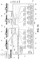
- FIG. 1C shows a fabric box 130 having a host interface of two PCIe links supporting 8 PCIe lanes.
- the fabric box 130 includes two PCIe switches 132 and 134.
- the PCIe switch 132 includes downstream ports 136a-136d that are connected to devices 70, 72, 74, and 76, respectively.
- the PCIe switch 134 includes downstream ports 138a-138d that are connected to devices 80, 82, 84, and 86, respectively.
- the switch 132 includes two upstream links 140 and 142 that are coupled to the host servers 30 and 32, respectively.
- the switch 134 includes two upstream links 144 and 146 that are coupled to the host servers 34 and 36, respectively.
- Each of the upstream links 140, 142, 144, and 146 includes two lanes, each through one cable. Therefore, there is one cable for each lane that connect respective upstream ports to ports on the host server.
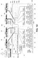
- FIG. 1D shows a fabric box 150 having a host interface of four PCIe links supporting 16 PCIe lanes. Like the fabric box, device and host server elements are labeled with identical element numbers in FIG. 1D as in FIG. 1A .
- the fabric box 150 includes two PCIe switches 152 and 154.
- the PCIe switch 152 includes downstream ports 156a-156d that are connected to devices 70, 72, 74, and 76, respectively.
- the PCIe switch 154 includes downstream ports 158a-158d that are connected to devices 80, 82, 84 and 86, respectively.
- the switch 152 includes two upstream links 160 and 162 that are coupled to the host servers 30 and 32, respectively.
- the switch 154 includes two upstream links 164 and 166 that are coupled to the host servers 34 and 36, respectively.
- Each of the upstream links 160, 162, 164, and 166 include four lanes. Therefore, there are four cables for each link that connect respective upstream ports to ports on the host server.
- FIG. 2A is a close up diagram of the correct cable connection between the switch 152 and the host server 30 in FIG. 1D .
- the PCIe link 160 has four lanes that include a series of four cables 170, 172, 174, and 176 that connect four respective upstream ports 180, 182, 184, and 186 of the switch 152.
- the other ends of cables 170, 172, 174, and 176 are connected to ports 190, 192, 194, and 196 of the host server 30.
- the group of ports on both the switch 152 and the host server 30 are connected in the same order. This configuration allows maximum speed for the PCIe link 160 as all four lanes may be used.
- FIG. 2B is a close up view of the system in FIG. 1D , where the cable 172 from the port 192 has been misconnected to the upstream port 184 of the PCIe switch 152.
- the cable 174 from the port 194 has also been misconnected to the upstream port 182 of the PCIe switch 152.
- This misconnection that changes the order of the ports is a misconfiguration case that will cause the PCIe speed of the link to be downgraded from 4 lanes to 1 lane.
- FIG. 2B therefore illustrates a relatively common occurrence where a user connects cables in the wrong order, resulting in a PCIe speed downgrade when the design uses multiple cables for a PCIe link group.
- One disclosed example is a system for insuring efficiency of a serial link between a host server and a fabric switch.
- the fabric switch has upstream ports associated with a serial link.
- the host server includes a BIOS and a management controller.
- the host server has ports coupled to the serial link ports via cables to form lanes of the serial link.
- a memory is accessible by the management controller.
- the management controller reads an expected speed and width of the serial link from the memory.
- the BIOS determines an actual speed and width of the serial link.
- the management controller sends an error message if the actual speed and width do not match the expected speed and width.
- Another disclosed example is a method to determine proper connections for a serial link between a host server and a fabric switch.
- the serial link has a plurality of lanes between ports of the host server and upstream ports of the fabric switch.
- the ports of the host server are connected with the upstream ports of the fabric switch via cables.
- An expected speed and width of the serial link is stored in a memory accessible by the host server.
- the expected speed and width of the serial link is read via the host server.
- An actual speed and width of the serial link is determined via the host server.
- the expected speed and width is compared with the actual speed and width.
- An error message is generated via the host server if the actual speed and width differ from the expected speed and width.
- FIG. 3 shows a block diagram of a system 200 for allocating device resources to different hosts.
- the system 200 includes a host server 202 that is coupled to a PCIe fabric box 210.
- the PCIe fabric box 210 includes numerous serial expansion bus devices such as Peripheral Component Interconnect Express (PCIe) compatible devices that may be accessed by the host server 202, or other devices in the data center.
- PCIe Peripheral Component Interconnect Express
- each host server such as the host server 202, has a PCIe link with multiple lanes connecting it to the PCIe fabric box 210.
- the multiple lanes are created by connected cables between ports of the host server 202 and the PCIe fabric box 210.
- the system 200 allows detection of such misconnections.
- the system 200
- the PCIe fabric box 210 includes a fabric controller 212 that may supervise the connection of device resources in the fabric box 210 to host servers such as the host server 202. Although only one host server 202 is shown, there may be multiple host servers connected to the PCIe fabric box 210 that may access the PCIe compatible devices.
- the fabric box 210 includes a memory device such as an EEPROM 214.
- the internal memory in the fabric controller 212 may also be used.
- the fabric controller 212 executes a control application to allocate devices to linked host servers, such as the host server 202, using a PCIe switch 216.
- the fabric box 210 may read data in the EEPROM 214 and may write data to the EEPROM 214.
- PCIe compatible devices 220, 222, 224, and 226 are coupled to respective downstream ports 230, 232, 234, and 236 of the PCIe switch 216.
- the PCIe compatible devices 220, 222, 224, and 226 may include a non-volatile memory (NVMe), a graphic processing unit (GPU), a field programmable gate array (FPGA), a network interface card (NIC), a redundant array of independent disks (RAID) interface card, an I-IBA card or other kinds of PCIe compatible devices.
- NVMe non-volatile memory
- GPU graphic processing unit
- FPGA field programmable gate array
- NIC network interface card
- RAID redundant array of independent disks
- the PCIe switch 216 is a PCIe device, different upstream ports 240, 242, 244, and 246 may each form a single PCIe link with four lanes.
- One end of a series of four cables 250, 252, 254, and 256 are connected to the upstream ports 240, 242, 244, and 246.
- the four cables 250, 252, 254, and 256 provide four lanes of a PCIe link between the fabric box 210 and the host server 202.
- Each lane may have more than one cable to increase the bandwidth of the lane. Higher capacity cable may allow one cable to be allocated for more than one lane.
- the PCIe switch 216 may have additional ports that may be organized into additional PCIe links. There may be additional PCIe switches similar to the PCIe switch 216, that allow additional links of variable width lanes in the fabric box 210.
- the host server 202 includes a baseboard management controller (BMC) 262 and a BIOS 264.
- the BMC 262 is coupled via an inter-integrated circuit (I2C) bus 266 to the EEPROM 214 and the fabric controller 212 of the fabric box 210.
- the I2C bus 266 may be a separate cable connecting the fabric box 210 to the host sever 202 or it may be an unused line on one of the cables 250, 252, 254, and 256.
- the BMC 262 may read data stored in the EEPROM 214. If the internal memory of the fabric controller 212 is used instead of the EEPROM 214, the BMC 262 may read data stored in the internal memory for the same purposes explained below.
- the host server 202 includes a PCIe root complex interface 268.
- the PCIe root interface 268 includes ports 270, 272, 274, and 276 that connect the other ends of the cables 250, 252, 254, and 256.
- the host server 202 and the switch 216 may have multiple other ports for additional lanes of other links to each other or other devices.
- the PCIe link formed by the cables 250, 252, 254, and 256 allow the host server 202 to access the devices 220, 222, 224, and 226 of the fabric box 210.
- one of the devices 220, 222, 224, and 226 may be a graphic processing unit that may be accessed by the host server through the PCIe switch 216 and some or all of the cables 250, 252, 254, and 256.
- the cables 250, 252, 254, and 256 must be connected in the correct order of the ports to insure maximum efficiency of the PCIe link connection by being able to use all the corresponding lanes.
- the inter-integrated circuit (I2C) bus 266 between the BMC 262 of the host server 202 and the fabric controller 212 allows both the BMC 262 and the controller 212 to share the EEPROM 214.
- data on the EEPROM 214 on PCIe fabric box 210 may be accessed by both the BMC 262 of the host server 202, and the fabric controller 212 of the PCIe fabric box 210.
- the fabric controller 212 programs hardware dependent, pre-defined information 280 to the EEPROM 214.
- the pre-defined information 280 includes the expected link speed of the connection between the host server 202 and the fabric box 210 and the link group width.
- the expected link speed in this example may be from a protocol standard such as PCIe Gen1, Gen 2, Gen 3, or Gen 4, or new version speeds of the PCIe standards. Alternatively, other protocols may be used.
- the link group width in this example is the number of lanes for the links, which may be 4, or 8, or 16 lanes, or more. The link width is determined by the initial configuration of the hardware in the system. In this example, each lane is formed by connecting a cable between ports of the host server 202 and the fabric box 210.
- the BMC 262 On connection of the I2C bus 266, the BMC 262 detects the EEPROM 214 and determines there is a PCIe fabric box connection to the host server 202. The BMC 262 reads the link speed and link group width from the EEPROM 214 and stores this information. The stored information in the BMC 262 is available to the BIOS 264. When the host server 202 powers on, the BIOS 264 gets the link speed and link group width from the BMC 262. The BIOS 264 performs PCIe bus training based on the link speed and link group width. Once the bus training is completed, the BIOS 264 obtains the current PCIe link speed and link width from the root complex interface 268.
- the training link speed and link group width result obtained by the BIOS 264 is compared with the link speed and link group width provided by the BMC 262. If the values do not match, the BIOS 264 will re-train several times to obtain the current link speed and link group width. The number of times, the BIOS 264 will perform retraining is predetermined by the system configuration. After the last retraining, the BIOS 264 will obtain a final PCIe current "Link Speed” and "Link Width" settings result. If the resulting current speed and width does not match to the expected speed and width values provided by the BMC 262, the BIOS 264 will generate an error log as the mismatch indicates that cables have been incorrectly connected to the ports.
- the BIOS 264 will update the final PCIe "Link Speed” and "Link Width" training result to the BMC 262.
- the BMC 262 will report the expected value by reading the stored data from the EEPROM 214 and the current training result of the BIOS 264 by an application programming interface (API).
- API application programming interface
- the host server 202 may generate an alert to an operator indicating a cable misconnection. The operator may obtain information about the decrease in link speed and therefore reconnect misconnected cables in the correct order.
- the below code segment is normal because the current speed and width match the expected speed and width, thus indicating that the cables forming the lanes of the link are properly connected to the respective ports of the host server 202 and the switch 216 of the fabric box 210.
- the link between the host server 202 and the fabric box 210 is at expected speed of 3 and an expected width of 16.
- FIG. 3 An example of a code segment that shows an error case result from the API is shown below.
- the current width is 8, but the expected width is 16, thereby indicating a cable misconnection.
- This error case may be caused by a cable in FIG. 3 being disconnected or misconnected.
- the cable 252 in FIG. 3 may be connecting the port 272 to the port 234; and the cable 254 connecting the port 274 to the port 232.
- the above code segments are examples of the output of one example API. However, the information in the code segments may be provided by other kinds of protocols or formats. If the expected values and current settings values do not match, the BMC 262 can report an error, and generate an entry in an event log. In this example, the operator may check the error by an API executed by the BMC 262.
- the API may provide data such as the expected speed and width of the link, and the current speed and width of the link, to assist an operator in diagnosis of the error.
- a flow diagram in FIG. 4 is representative of example machine readable instructions for checking proper cable connection by the fabric controller 212, BMC 262, and BIOS 264 in FIG. 3 .
- the machine readable instructions comprise an algorithm for execution by: (a) a processor; (b) a controller; and/or (c) one or more other suitable processing device(s).
- the algorithm may be embodied in software stored on tangible media such as flash memory, CD-ROM, floppy disk, hard drive, digital video (versatile) disk (DVD), or other memory devices.
- the link speed and link group width for the links from the PCIe switch 216 is stored in the EEPROM 214 by the fabric controller 212 (400).
- the BMC 262 detects the stored link speed and link group width information and determines that there is a PCIe link between the host server 202 and the PCIe switch 216 (402).
- the BMC 262 reads the stored link speed and link group width information and stores the information (404).
- the BIOS 264 obtains the link speed and link group width information from the BMC 262 (406).
- the BIOS 264 then begins a training routine for the PCIe bus to obtain the current link speed and link group width from the PCIe root complex 268 (408). Once training is complete, the BIOS 264 obtains the current link speed and link group width (410).
- the training result is compared with the current link speed and link group width (412). If the training result matches the current link speed and link group width, the BIOS 264 will end the check routine (414). If the training result does not match, the BIOS 264 will retrain to obtain the current link speed and link group width from the PCIe root complex 268 (416). After retraining, the BIOS 264 will determine whether the retraining result matches the current link speed and link group width (418). If the retraining result matches the current link speed and link group width, the BIOS 264 will end the check routine (414). If the retraining result does not match, the BIOS 264 will generate an error log entry (420). The BMC 262 will report the expected value from the EEPROM 214 and the current value from the BIOS 264 (422).
- a component generally refer to a computer-related entity, either hardware (e.g., a circuit), a combination of hardware and software, software, or an entity related to an operational machine with one or more specific functionalities.
- a component may be, but is not limited to being, a process running on a processor (e.g., digital signal processor), a processor, an object, an executable, a thread of execution, a program, and/or a computer.
- a processor e.g., digital signal processor
- an application running on a controller as well as the controller, can be a component.
- One or more components may reside within a process and/or thread of execution, and a component may be localized on one computer and/or distributed between two or more computers.
- a “device” can come in the form of specially designed hardware; generalized hardware made specialized by the execution of software thereon that enables the hardware to perform specific function; software stored on a computer-readable medium; or a combination thereof.
Landscapes
- Engineering & Computer Science (AREA)
- Theoretical Computer Science (AREA)
- Physics & Mathematics (AREA)
- General Engineering & Computer Science (AREA)
- General Physics & Mathematics (AREA)
- Mathematical Physics (AREA)
- Computer Hardware Design (AREA)
- Quality & Reliability (AREA)
- Information Transfer Systems (AREA)
Applications Claiming Priority (2)
| Application Number | Priority Date | Filing Date | Title |
|---|---|---|---|
| US201862649734P | 2018-03-29 | 2018-03-29 | |
| US16/041,065 US10657080B2 (en) | 2018-03-29 | 2018-07-20 | Method and system for checking errors on cables |
Publications (2)
| Publication Number | Publication Date |
|---|---|
| EP3547149A1 true EP3547149A1 (de) | 2019-10-02 |
| EP3547149B1 EP3547149B1 (de) | 2021-06-16 |
Family
ID=64402089
Family Applications (1)
| Application Number | Title | Priority Date | Filing Date |
|---|---|---|---|
| EP18207259.5A Active EP3547149B1 (de) | 2018-03-29 | 2018-11-20 | Verfahren und system zur prüfung von fehlern an kabeln |
Country Status (5)
| Country | Link |
|---|---|
| US (1) | US10657080B2 (de) |
| EP (1) | EP3547149B1 (de) |
| JP (1) | JP6662987B2 (de) |
| CN (1) | CN110321255B (de) |
| TW (1) | TW201942756A (de) |
Cited By (1)
| Publication number | Priority date | Publication date | Assignee | Title |
|---|---|---|---|---|
| CN112783816A (zh) * | 2021-01-04 | 2021-05-11 | 东风汽车股份有限公司 | 一种手持式双串口协议捕获与分析诊断仪及其使用方法 |
Families Citing this family (4)
| Publication number | Priority date | Publication date | Assignee | Title |
|---|---|---|---|---|
| US11243859B2 (en) * | 2019-10-09 | 2022-02-08 | Microsoft Technology Licensing, Llc | Baseboard management controller that initiates a diagnostic operation to collect host information |
| US11509751B2 (en) * | 2020-12-23 | 2022-11-22 | Dell Products L.P. | Self-describing system using single-source/multi-destination cable |
| CN114826489B (zh) * | 2022-05-29 | 2023-07-14 | 苏州浪潮智能科技有限公司 | 一种链路纠错方法、系统、存储介质及设备 |
| CN115904835A (zh) * | 2022-11-07 | 2023-04-04 | 超聚变数字技术有限公司 | 一种线缆检测方法及服务器 |
Citations (3)
| Publication number | Priority date | Publication date | Assignee | Title |
|---|---|---|---|---|
| US20150254200A1 (en) * | 2014-03-06 | 2015-09-10 | International Business Machines Corporation | PERIPHERAL COMPONENT INTERCONNECT EXPRESS (PCIe) PING IN A SWITCH-BASED ENVIRONMENT |
| US20150324268A1 (en) * | 2014-04-02 | 2015-11-12 | Huawei Technologies Co., Ltd. | Method, Device, and System for Processing PCIe Link Fault |
| US20160147705A1 (en) * | 2014-11-21 | 2016-05-26 | International Business Machines Corporation | Implementing health check for optical cable attached pcie enclosure |
Family Cites Families (6)
| Publication number | Priority date | Publication date | Assignee | Title |
|---|---|---|---|---|
| JP2009163633A (ja) * | 2008-01-09 | 2009-07-23 | Ricoh Co Ltd | 情報処理装置およびデータ通信方法 |
| TWI437493B (zh) * | 2011-07-25 | 2014-05-11 | Quanta Comp Inc | 電腦系統及其作業系統載入方法 |
| JP2013117930A (ja) * | 2011-12-05 | 2013-06-13 | Hitachi Ltd | 計算機及び計算機の制御方法 |
| WO2015111206A1 (ja) * | 2014-01-27 | 2015-07-30 | 株式会社日立製作所 | 計算機システム、サーバモジュール及びストレージモジュール |
| US10007441B2 (en) * | 2014-04-30 | 2018-06-26 | Hewlett Packard Enterprise Development Lp | Storage system bandwidth adjustment |
| WO2015194534A1 (ja) * | 2014-06-17 | 2015-12-23 | 日本電気株式会社 | スイッチ装置とコンピュータシステムと方法並びにプログラム |
-
2018
- 2018-07-20 US US16/041,065 patent/US10657080B2/en active Active
- 2018-10-26 TW TW107138098A patent/TW201942756A/zh unknown
- 2018-11-08 CN CN201811323405.3A patent/CN110321255B/zh active Active
- 2018-11-20 EP EP18207259.5A patent/EP3547149B1/de active Active
- 2018-11-22 JP JP2018219045A patent/JP6662987B2/ja active Active
Patent Citations (3)
| Publication number | Priority date | Publication date | Assignee | Title |
|---|---|---|---|---|
| US20150254200A1 (en) * | 2014-03-06 | 2015-09-10 | International Business Machines Corporation | PERIPHERAL COMPONENT INTERCONNECT EXPRESS (PCIe) PING IN A SWITCH-BASED ENVIRONMENT |
| US20150324268A1 (en) * | 2014-04-02 | 2015-11-12 | Huawei Technologies Co., Ltd. | Method, Device, and System for Processing PCIe Link Fault |
| US20160147705A1 (en) * | 2014-11-21 | 2016-05-26 | International Business Machines Corporation | Implementing health check for optical cable attached pcie enclosure |
Cited By (2)
| Publication number | Priority date | Publication date | Assignee | Title |
|---|---|---|---|---|
| CN112783816A (zh) * | 2021-01-04 | 2021-05-11 | 东风汽车股份有限公司 | 一种手持式双串口协议捕获与分析诊断仪及其使用方法 |
| CN112783816B (zh) * | 2021-01-04 | 2022-07-22 | 东风汽车股份有限公司 | 一种手持式双串口协议捕获与分析诊断仪及其使用方法 |
Also Published As
| Publication number | Publication date |
|---|---|
| EP3547149B1 (de) | 2021-06-16 |
| JP6662987B2 (ja) | 2020-03-11 |
| US10657080B2 (en) | 2020-05-19 |
| CN110321255B (zh) | 2022-11-08 |
| CN110321255A (zh) | 2019-10-11 |
| JP2019175424A (ja) | 2019-10-10 |
| TW201942756A (zh) | 2019-11-01 |
| US20190303315A1 (en) | 2019-10-03 |
Similar Documents
| Publication | Publication Date | Title |
|---|---|---|
| EP3547149B1 (de) | Verfahren und system zur prüfung von fehlern an kabeln | |
| CN106603265B (zh) | 管理方法、网络装置以及非暂态计算机可读介质 | |
| US8948000B2 (en) | Switch fabric management | |
| US10127095B2 (en) | Seamless automatic recovery of a switch device | |
| US7676694B2 (en) | Managing system components | |
| CN103124225B (zh) | 多节点初始化的检测方法及装置、系统 | |
| US10853213B2 (en) | Validation of installation of removeable computer hardware components | |
| TWI777628B (zh) | 電腦系統及其專用崩潰轉存硬體裝置與記錄錯誤資料之方法 | |
| CN119383170B (zh) | 一种地址配置方法、设备、存储介质及程序产品 | |
| WO2023129298A1 (en) | Systems and methods to initiate device recovery | |
| WO2026037009A1 (zh) | 带宽分配方法、服务器、设备、介质及程序产品 | |
| US7793145B2 (en) | Method and apparatus for verifying fault tolerant configuration | |
| CN105549696A (zh) | 具有机箱管理功能的机架式服务器系统 | |
| US20180145869A1 (en) | Debugging method of switches | |
| US10664428B2 (en) | SAS automatic zoning mechanism | |
| US20250130967A1 (en) | Systems and methods to preconfigure a hardware module | |
| CN104252400A (zh) | 数据中心多节点管理系统及方法 | |
| CN120874096B (zh) | 一种访问控制服务设置方法及电子设备 | |
| US12608330B2 (en) | Individual power cycle control of accelerator modules configured on a node | |
| CN119311625A (zh) | PCIe资产信息的生成方法、装置及程序产品 | |
| CN112100109A (zh) | 一种线缆连接容错连接装置及方法 |
Legal Events
| Date | Code | Title | Description |
|---|---|---|---|
| PUAI | Public reference made under article 153(3) epc to a published international application that has entered the european phase |
Free format text: ORIGINAL CODE: 0009012 |
|
| STAA | Information on the status of an ep patent application or granted ep patent |
Free format text: STATUS: THE APPLICATION HAS BEEN PUBLISHED |
|
| AK | Designated contracting states |
Kind code of ref document: A1 Designated state(s): AL AT BE BG CH CY CZ DE DK EE ES FI FR GB GR HR HU IE IS IT LI LT LU LV MC MK MT NL NO PL PT RO RS SE SI SK SM TR |
|
| AX | Request for extension of the european patent |
Extension state: BA ME |
|
| STAA | Information on the status of an ep patent application or granted ep patent |
Free format text: STATUS: REQUEST FOR EXAMINATION WAS MADE |
|
| 17P | Request for examination filed |
Effective date: 20190925 |
|
| RBV | Designated contracting states (corrected) |
Designated state(s): AL AT BE BG CH CY CZ DE DK EE ES FI FR GB GR HR HU IE IS IT LI LT LU LV MC MK MT NL NO PL PT RO RS SE SI SK SM TR |
|
| STAA | Information on the status of an ep patent application or granted ep patent |
Free format text: STATUS: EXAMINATION IS IN PROGRESS |
|
| 17Q | First examination report despatched |
Effective date: 20200217 |
|
| GRAP | Despatch of communication of intention to grant a patent |
Free format text: ORIGINAL CODE: EPIDOSNIGR1 |
|
| STAA | Information on the status of an ep patent application or granted ep patent |
Free format text: STATUS: GRANT OF PATENT IS INTENDED |
|
| INTG | Intention to grant announced |
Effective date: 20210317 |
|
| GRAS | Grant fee paid |
Free format text: ORIGINAL CODE: EPIDOSNIGR3 |
|
| GRAA | (expected) grant |
Free format text: ORIGINAL CODE: 0009210 |
|
| STAA | Information on the status of an ep patent application or granted ep patent |
Free format text: STATUS: THE PATENT HAS BEEN GRANTED |
|
| AK | Designated contracting states |
Kind code of ref document: B1 Designated state(s): AL AT BE BG CH CY CZ DE DK EE ES FI FR GB GR HR HU IE IS IT LI LT LU LV MC MK MT NL NO PL PT RO RS SE SI SK SM TR |
|
| REG | Reference to a national code |
Ref country code: GB Ref legal event code: FG4D |
|
| REG | Reference to a national code |
Ref country code: CH Ref legal event code: EP |
|
| REG | Reference to a national code |
Ref country code: DE Ref legal event code: R096 Ref document number: 602018018615 Country of ref document: DE |
|
| REG | Reference to a national code |
Ref country code: AT Ref legal event code: REF Ref document number: 1402911 Country of ref document: AT Kind code of ref document: T Effective date: 20210715 |
|
| REG | Reference to a national code |
Ref country code: IE Ref legal event code: FG4D |
|
| REG | Reference to a national code |
Ref country code: LT Ref legal event code: MG9D |
|
| PG25 | Lapsed in a contracting state [announced via postgrant information from national office to epo] |
Ref country code: BG Free format text: LAPSE BECAUSE OF FAILURE TO SUBMIT A TRANSLATION OF THE DESCRIPTION OR TO PAY THE FEE WITHIN THE PRESCRIBED TIME-LIMIT Effective date: 20210916 Ref country code: FI Free format text: LAPSE BECAUSE OF FAILURE TO SUBMIT A TRANSLATION OF THE DESCRIPTION OR TO PAY THE FEE WITHIN THE PRESCRIBED TIME-LIMIT Effective date: 20210616 Ref country code: LT Free format text: LAPSE BECAUSE OF FAILURE TO SUBMIT A TRANSLATION OF THE DESCRIPTION OR TO PAY THE FEE WITHIN THE PRESCRIBED TIME-LIMIT Effective date: 20210616 Ref country code: HR Free format text: LAPSE BECAUSE OF FAILURE TO SUBMIT A TRANSLATION OF THE DESCRIPTION OR TO PAY THE FEE WITHIN THE PRESCRIBED TIME-LIMIT Effective date: 20210616 |
|
| REG | Reference to a national code |
Ref country code: AT Ref legal event code: MK05 Ref document number: 1402911 Country of ref document: AT Kind code of ref document: T Effective date: 20210616 |
|
| REG | Reference to a national code |
Ref country code: NL Ref legal event code: MP Effective date: 20210616 |
|
| PG25 | Lapsed in a contracting state [announced via postgrant information from national office to epo] |
Ref country code: GR Free format text: LAPSE BECAUSE OF FAILURE TO SUBMIT A TRANSLATION OF THE DESCRIPTION OR TO PAY THE FEE WITHIN THE PRESCRIBED TIME-LIMIT Effective date: 20210917 Ref country code: RS Free format text: LAPSE BECAUSE OF FAILURE TO SUBMIT A TRANSLATION OF THE DESCRIPTION OR TO PAY THE FEE WITHIN THE PRESCRIBED TIME-LIMIT Effective date: 20210616 Ref country code: SE Free format text: LAPSE BECAUSE OF FAILURE TO SUBMIT A TRANSLATION OF THE DESCRIPTION OR TO PAY THE FEE WITHIN THE PRESCRIBED TIME-LIMIT Effective date: 20210616 Ref country code: LV Free format text: LAPSE BECAUSE OF FAILURE TO SUBMIT A TRANSLATION OF THE DESCRIPTION OR TO PAY THE FEE WITHIN THE PRESCRIBED TIME-LIMIT Effective date: 20210616 Ref country code: NO Free format text: LAPSE BECAUSE OF FAILURE TO SUBMIT A TRANSLATION OF THE DESCRIPTION OR TO PAY THE FEE WITHIN THE PRESCRIBED TIME-LIMIT Effective date: 20210916 |
|
| PG25 | Lapsed in a contracting state [announced via postgrant information from national office to epo] |
Ref country code: EE Free format text: LAPSE BECAUSE OF FAILURE TO SUBMIT A TRANSLATION OF THE DESCRIPTION OR TO PAY THE FEE WITHIN THE PRESCRIBED TIME-LIMIT Effective date: 20210616 Ref country code: ES Free format text: LAPSE BECAUSE OF FAILURE TO SUBMIT A TRANSLATION OF THE DESCRIPTION OR TO PAY THE FEE WITHIN THE PRESCRIBED TIME-LIMIT Effective date: 20210616 Ref country code: SK Free format text: LAPSE BECAUSE OF FAILURE TO SUBMIT A TRANSLATION OF THE DESCRIPTION OR TO PAY THE FEE WITHIN THE PRESCRIBED TIME-LIMIT Effective date: 20210616 Ref country code: SM Free format text: LAPSE BECAUSE OF FAILURE TO SUBMIT A TRANSLATION OF THE DESCRIPTION OR TO PAY THE FEE WITHIN THE PRESCRIBED TIME-LIMIT Effective date: 20210616 Ref country code: RO Free format text: LAPSE BECAUSE OF FAILURE TO SUBMIT A TRANSLATION OF THE DESCRIPTION OR TO PAY THE FEE WITHIN THE PRESCRIBED TIME-LIMIT Effective date: 20210616 Ref country code: PT Free format text: LAPSE BECAUSE OF FAILURE TO SUBMIT A TRANSLATION OF THE DESCRIPTION OR TO PAY THE FEE WITHIN THE PRESCRIBED TIME-LIMIT Effective date: 20211018 Ref country code: NL Free format text: LAPSE BECAUSE OF FAILURE TO SUBMIT A TRANSLATION OF THE DESCRIPTION OR TO PAY THE FEE WITHIN THE PRESCRIBED TIME-LIMIT Effective date: 20210616 Ref country code: AT Free format text: LAPSE BECAUSE OF FAILURE TO SUBMIT A TRANSLATION OF THE DESCRIPTION OR TO PAY THE FEE WITHIN THE PRESCRIBED TIME-LIMIT Effective date: 20210616 Ref country code: CZ Free format text: LAPSE BECAUSE OF FAILURE TO SUBMIT A TRANSLATION OF THE DESCRIPTION OR TO PAY THE FEE WITHIN THE PRESCRIBED TIME-LIMIT Effective date: 20210616 |
|
| PG25 | Lapsed in a contracting state [announced via postgrant information from national office to epo] |
Ref country code: PL Free format text: LAPSE BECAUSE OF FAILURE TO SUBMIT A TRANSLATION OF THE DESCRIPTION OR TO PAY THE FEE WITHIN THE PRESCRIBED TIME-LIMIT Effective date: 20210616 |
|
| REG | Reference to a national code |
Ref country code: DE Ref legal event code: R097 Ref document number: 602018018615 Country of ref document: DE |
|
| PLBE | No opposition filed within time limit |
Free format text: ORIGINAL CODE: 0009261 |
|
| STAA | Information on the status of an ep patent application or granted ep patent |
Free format text: STATUS: NO OPPOSITION FILED WITHIN TIME LIMIT |
|
| PG25 | Lapsed in a contracting state [announced via postgrant information from national office to epo] |
Ref country code: DK Free format text: LAPSE BECAUSE OF FAILURE TO SUBMIT A TRANSLATION OF THE DESCRIPTION OR TO PAY THE FEE WITHIN THE PRESCRIBED TIME-LIMIT Effective date: 20210616 |
|
| 26N | No opposition filed |
Effective date: 20220317 |
|
| PG25 | Lapsed in a contracting state [announced via postgrant information from national office to epo] |
Ref country code: AL Free format text: LAPSE BECAUSE OF FAILURE TO SUBMIT A TRANSLATION OF THE DESCRIPTION OR TO PAY THE FEE WITHIN THE PRESCRIBED TIME-LIMIT Effective date: 20210616 |
|
| PG25 | Lapsed in a contracting state [announced via postgrant information from national office to epo] |
Ref country code: MC Free format text: LAPSE BECAUSE OF FAILURE TO SUBMIT A TRANSLATION OF THE DESCRIPTION OR TO PAY THE FEE WITHIN THE PRESCRIBED TIME-LIMIT Effective date: 20210616 |
|
| REG | Reference to a national code |
Ref country code: CH Ref legal event code: PL |
|
| PG25 | Lapsed in a contracting state [announced via postgrant information from national office to epo] |
Ref country code: LU Free format text: LAPSE BECAUSE OF NON-PAYMENT OF DUE FEES Effective date: 20211120 Ref country code: IT Free format text: LAPSE BECAUSE OF FAILURE TO SUBMIT A TRANSLATION OF THE DESCRIPTION OR TO PAY THE FEE WITHIN THE PRESCRIBED TIME-LIMIT Effective date: 20210616 Ref country code: BE Free format text: LAPSE BECAUSE OF NON-PAYMENT OF DUE FEES Effective date: 20211130 |
|
| REG | Reference to a national code |
Ref country code: BE Ref legal event code: MM Effective date: 20211130 |
|
| PG25 | Lapsed in a contracting state [announced via postgrant information from national office to epo] |
Ref country code: LI Free format text: LAPSE BECAUSE OF NON-PAYMENT OF DUE FEES Effective date: 20211130 Ref country code: CH Free format text: LAPSE BECAUSE OF NON-PAYMENT OF DUE FEES Effective date: 20211130 |
|
| PG25 | Lapsed in a contracting state [announced via postgrant information from national office to epo] |
Ref country code: IE Free format text: LAPSE BECAUSE OF NON-PAYMENT OF DUE FEES Effective date: 20211120 |
|
| P01 | Opt-out of the competence of the unified patent court (upc) registered |
Effective date: 20230522 |
|
| PG25 | Lapsed in a contracting state [announced via postgrant information from national office to epo] |
Ref country code: CY Free format text: LAPSE BECAUSE OF FAILURE TO SUBMIT A TRANSLATION OF THE DESCRIPTION OR TO PAY THE FEE WITHIN THE PRESCRIBED TIME-LIMIT Effective date: 20210616 |
|
| PG25 | Lapsed in a contracting state [announced via postgrant information from national office to epo] |
Ref country code: HU Free format text: LAPSE BECAUSE OF FAILURE TO SUBMIT A TRANSLATION OF THE DESCRIPTION OR TO PAY THE FEE WITHIN THE PRESCRIBED TIME-LIMIT; INVALID AB INITIO Effective date: 20181120 |
|
| PG25 | Lapsed in a contracting state [announced via postgrant information from national office to epo] |
Ref country code: MK Free format text: LAPSE BECAUSE OF FAILURE TO SUBMIT A TRANSLATION OF THE DESCRIPTION OR TO PAY THE FEE WITHIN THE PRESCRIBED TIME-LIMIT Effective date: 20210616 |
|
| PG25 | Lapsed in a contracting state [announced via postgrant information from national office to epo] |
Ref country code: TR Free format text: LAPSE BECAUSE OF FAILURE TO SUBMIT A TRANSLATION OF THE DESCRIPTION OR TO PAY THE FEE WITHIN THE PRESCRIBED TIME-LIMIT Effective date: 20210616 |
|
| PG25 | Lapsed in a contracting state [announced via postgrant information from national office to epo] |
Ref country code: MT Free format text: LAPSE BECAUSE OF FAILURE TO SUBMIT A TRANSLATION OF THE DESCRIPTION OR TO PAY THE FEE WITHIN THE PRESCRIBED TIME-LIMIT Effective date: 20210616 |
|
| PGFP | Annual fee paid to national office [announced via postgrant information from national office to epo] |
Ref country code: GB Payment date: 20250930 Year of fee payment: 8 |
|
| PGFP | Annual fee paid to national office [announced via postgrant information from national office to epo] |
Ref country code: FR Payment date: 20250922 Year of fee payment: 8 |
|
| PGFP | Annual fee paid to national office [announced via postgrant information from national office to epo] |
Ref country code: DE Payment date: 20250923 Year of fee payment: 8 |