EP3544126B1 - Device having usb port - Google Patents
Device having usb port Download PDFInfo
- Publication number
- EP3544126B1 EP3544126B1 EP16923157.8A EP16923157A EP3544126B1 EP 3544126 B1 EP3544126 B1 EP 3544126B1 EP 16923157 A EP16923157 A EP 16923157A EP 3544126 B1 EP3544126 B1 EP 3544126B1
- Authority
- EP
- European Patent Office
- Prior art keywords
- area
- usb port
- electronic device
- cabling
- cable
- Prior art date
- Legal status (The legal status is an assumption and is not a legal conclusion. Google has not performed a legal analysis and makes no representation as to the accuracy of the status listed.)
- Active
Links
Images



Classifications
-
- G—PHYSICS
- G06—COMPUTING OR CALCULATING; COUNTING
- G06F—ELECTRIC DIGITAL DATA PROCESSING
- G06F13/00—Interconnection of, or transfer of information or other signals between, memories, input/output devices or central processing units
- G06F13/38—Information transfer, e.g. on bus
- G06F13/40—Bus structure
- G06F13/4063—Device-to-bus coupling
- G06F13/4068—Electrical coupling
- G06F13/4072—Drivers or receivers
- G06F13/4077—Precharging or discharging
-
- H—ELECTRICITY
- H01—ELECTRIC ELEMENTS
- H01R—ELECTRICALLY-CONDUCTIVE CONNECTIONS; STRUCTURAL ASSOCIATIONS OF A PLURALITY OF MUTUALLY-INSULATED ELECTRICAL CONNECTING ELEMENTS; COUPLING DEVICES; CURRENT COLLECTORS
- H01R13/00—Details of coupling devices of the kinds covered by groups H01R12/70 or H01R24/00 - H01R33/00
- H01R13/66—Structural association with built-in electrical component
- H01R13/6608—Structural association with built-in electrical component with built-in single component
- H01R13/6625—Structural association with built-in electrical component with built-in single component with capacitive component
-
- H—ELECTRICITY
- H01—ELECTRIC ELEMENTS
- H01R—ELECTRICALLY-CONDUCTIVE CONNECTIONS; STRUCTURAL ASSOCIATIONS OF A PLURALITY OF MUTUALLY-INSULATED ELECTRICAL CONNECTING ELEMENTS; COUPLING DEVICES; CURRENT COLLECTORS
- H01R13/00—Details of coupling devices of the kinds covered by groups H01R12/70 or H01R24/00 - H01R33/00
- H01R13/648—Protective earth or shield arrangements on coupling devices, e.g. anti-static shielding
-
- H—ELECTRICITY
- H01—ELECTRIC ELEMENTS
- H01R—ELECTRICALLY-CONDUCTIVE CONNECTIONS; STRUCTURAL ASSOCIATIONS OF A PLURALITY OF MUTUALLY-INSULATED ELECTRICAL CONNECTING ELEMENTS; COUPLING DEVICES; CURRENT COLLECTORS
- H01R13/00—Details of coupling devices of the kinds covered by groups H01R12/70 or H01R24/00 - H01R33/00
- H01R13/648—Protective earth or shield arrangements on coupling devices, e.g. anti-static shielding
- H01R13/658—High frequency shielding arrangements, e.g. against EMI [Electro-Magnetic Interference] or EMP [Electro-Magnetic Pulse]
- H01R13/6591—Specific features or arrangements of connection of shield to conductive members
- H01R13/6594—Specific features or arrangements of connection of shield to conductive members the shield being mounted on a PCB and connected to conductive members
-
- H—ELECTRICITY
- H01—ELECTRIC ELEMENTS
- H01R—ELECTRICALLY-CONDUCTIVE CONNECTIONS; STRUCTURAL ASSOCIATIONS OF A PLURALITY OF MUTUALLY-INSULATED ELECTRICAL CONNECTING ELEMENTS; COUPLING DEVICES; CURRENT COLLECTORS
- H01R13/00—Details of coupling devices of the kinds covered by groups H01R12/70 or H01R24/00 - H01R33/00
- H01R13/66—Structural association with built-in electrical component
- H01R13/719—Structural association with built-in electrical component specially adapted for high frequency, e.g. with filters
- H01R13/7195—Structural association with built-in electrical component specially adapted for high frequency, e.g. with filters with planar filters with openings for contacts
-
- H—ELECTRICITY
- H05—ELECTRIC TECHNIQUES NOT OTHERWISE PROVIDED FOR
- H05K—PRINTED CIRCUITS; CASINGS OR CONSTRUCTIONAL DETAILS OF ELECTRIC APPARATUS; MANUFACTURE OF ASSEMBLAGES OF ELECTRICAL COMPONENTS
- H05K1/00—Printed circuits
- H05K1/02—Details
- H05K1/0213—Electrical arrangements not otherwise provided for
- H05K1/0216—Reduction of cross-talk, noise or electromagnetic interference
- H05K1/023—Reduction of cross-talk, noise or electromagnetic interference using auxiliary mounted passive components or auxiliary substances
- H05K1/0231—Capacitors or dielectric substances
-
- H—ELECTRICITY
- H05—ELECTRIC TECHNIQUES NOT OTHERWISE PROVIDED FOR
- H05K—PRINTED CIRCUITS; CASINGS OR CONSTRUCTIONAL DETAILS OF ELECTRIC APPARATUS; MANUFACTURE OF ASSEMBLAGES OF ELECTRICAL COMPONENTS
- H05K1/00—Printed circuits
- H05K1/16—Printed circuits incorporating printed electric components, e.g. printed resistors, capacitors or inductors
- H05K1/162—Printed circuits incorporating printed electric components, e.g. printed resistors, capacitors or inductors incorporating printed capacitors
-
- H—ELECTRICITY
- H05—ELECTRIC TECHNIQUES NOT OTHERWISE PROVIDED FOR
- H05K—PRINTED CIRCUITS; CASINGS OR CONSTRUCTIONAL DETAILS OF ELECTRIC APPARATUS; MANUFACTURE OF ASSEMBLAGES OF ELECTRICAL COMPONENTS
- H05K1/00—Printed circuits
- H05K1/18—Printed circuits structurally associated with non-printed electric components
- H05K1/182—Printed circuits structurally associated with non-printed electric components associated with components mounted in printed circuit boards [PCB], e.g. insert-mounted components [IMC]
-
- H—ELECTRICITY
- H05—ELECTRIC TECHNIQUES NOT OTHERWISE PROVIDED FOR
- H05K—PRINTED CIRCUITS; CASINGS OR CONSTRUCTIONAL DETAILS OF ELECTRIC APPARATUS; MANUFACTURE OF ASSEMBLAGES OF ELECTRICAL COMPONENTS
- H05K1/00—Printed circuits
- H05K1/02—Details
- H05K1/0213—Electrical arrangements not otherwise provided for
- H05K1/0237—High frequency adaptations
- H05K1/025—Impedance arrangements, e.g. impedance matching, reduction of parasitic impedance
-
- H—ELECTRICITY
- H05—ELECTRIC TECHNIQUES NOT OTHERWISE PROVIDED FOR
- H05K—PRINTED CIRCUITS; CASINGS OR CONSTRUCTIONAL DETAILS OF ELECTRIC APPARATUS; MANUFACTURE OF ASSEMBLAGES OF ELECTRICAL COMPONENTS
- H05K2201/00—Indexing scheme relating to printed circuits covered by H05K1/00
- H05K2201/09—Shape and layout
- H05K2201/09209—Shape and layout details of conductors
- H05K2201/09654—Shape and layout details of conductors covering at least two types of conductors provided for in H05K2201/09218 - H05K2201/095
- H05K2201/09781—Dummy conductors, i.e. not used for normal transport of current; Dummy electrodes of components
Definitions
- the present invention relates to the field of USB connection technologies, and in particular, to a device with a USB port.
- an electronic device such as a smartphone or a tablet personal computer performs charging, data transmission, and the like by using a USB port.
- Two or four fixed contacts 11 are usually disposed on a metal housing of the universal serial bus (universal serial bus, USB) port on the electronic device, and the USB port on the electronic device is fastened to a printed circuit board (printed circuit board, PCB) of the electronic device by using the fixed contacts 11.
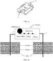
- the metal housing of the USB port is usually connected to a ground (as shown in FIG. 1b ) on the PCB of the electronic device by using the fixed contacts 11. Because the metal housing of the USB port is relatively close to a USB tongue, non-insulation materials such as perspiration and dust particles accumulate between the tongue and the metal housing of the USB port in daily use, especially between the USB housing and a power pin (VBUS) on the tongue (as shown in FIG.
- the USB port is usually disposed at a lower part of the electronic device such as a mobile phone, and usually an antenna is also disposed at the lower part of the electronic device.
- the antenna is interfered with.
- the metal housing of the USB port is usually connected to the ground on the PCB of the electronic device by using an additional protection component.
- the protection component is configured to interference and prevent a micro short circuit.
- the protection component occupies internal space of the electronic device. Consequently, it is not conducive to lightening and thinning of the electronic device.
- EP0875963 discloses a filtered universal serial bus.
- the capacitive filter element 74 in EP0875963 has been identified as the printed circuit board. However it cannot be considered that the capacitive filter element comprises two cabling layers.
- the conductive plane 92 and the signal electrode 94 cannot be considered as cabling layers of the printed circuit board, since they are exclusively directed to provide the capacitor.
- EP1419559 relates to suppression of common electrical noise on the cable braid for the reduction of electromagnetic emissions in high-speed differential serial link cable connectors using technique applicable to the printed circuit board (PCB) on which this cable connector is mounted.
- the method involves providing a connector shell and connecting printed circuit board capacitor plates in a signal layer metallization (21,22,23,24) directly to the connector shell by means of connector pins 70 and providing low impedance alternating current path to logic ground layers (11,12,13).
- the high frequency low impedance alternating current path (2) comprises a plurality of metal plates in a plurality of signal layers (21, 22, 23, 24) forming a plurality of capacitor plates in parallel coupled between the connector shell (7) and a plurality of logic ground layers (11).
- the connector pins 60 connecting the connector outer shell to the various signal layer metallizations passes through multiple vias 51 through logic ground layer I and onto signal layer metallization 22 without making an electrical connection to logic ground 11.
- Embodiments of the present invention provide an electronic device, a USB cable, and a charger, so that a short circuit of a USB port is prevented, interference of the USB port is shielded, and internal space of the electronic device is not occupied.
- the metal housing of the USB port of the electronic device is not connected to the ground of the PCB, so that a short circuit does not occur.
- a floating area and a metal area opposite to the floating area are disposed on the PCB, and the metal housing of the USB port of the electronic device is connected to the floating area, so as to form a capacitor, thereby preventing an antenna from being interfered with by the USB port.
- capacitance formed by the first floating area and the first metal area is ⁇ ⁇ s 4 ⁇ ⁇ ⁇ k ⁇ d , where s is an area of overlap of the first floating area and the first metal area, d is a distance between the first floating area and the first metal area, ⁇ is a dielectric constant of the insulation medium, and k is an electrostatic constant.
- the PCB includes a second floating area, the second floating area is located at the first cabling layer, the second cabling layer has a second metal area, an orthographic projection of the second floating area on the second cabling layer and the second metal area have an overlapping area, and the second floating area is not connected to the second metal area; and the plurality of fixed contacts of the USB port include a second fixed contact, the second fixed contact is connected to the second floating area, and the second fixed contact is not connected to the second metal area.
- a third cabling layer in the at least two cabling layers include a third floating area, a fourth cabling layer in the at least two cabling layers and the third cabling layer are adjacent and isolated by using the insulation medium, the fourth cabling layer is disposed with a third metal area, an orthographic projection of the third floating area on the fourth cabling layer and the third metal area have an overlapping area, and the third floating area is not connected to the third metal area; and the first fixed contact is connected to the first floating area and the third floating area, and the first fixed contact is not connected to the first metal area and the third metal area.
- the first cabling layer is not adjacent to the third cabling layer.
- a distance between the first cabling layer and the third cabling layer is greater than a distance between the first cabling layer and the second cabling layer, and is greater than a distance between the third cabling layer and the fourth cabling layer.
- the first metal area is the ground of the PCB. Therefore, noise backflow can be better implemented.
- a second aspect provides that the electronic device is a charger.
- An electronic device may be a mobile phone (also referred to as a smartphone), a tablet personal computer (Tablet Personal Computer), a personal digital assistant (personal digital assistant, PDA for short), an e-book reader (English: e-book reader) or a wearable device (Wearable Device), a virtual reality interactive device (Virtual Reality Interactive Device), or the like.
- the electronic device may establish communication with a network by using a 2G (second generation mobile phone communications technical specification), a 3G (third generation mobile phone communications technical specification), a 4G (fourth generation mobile phone communications technical specification), a 5G (fifth generation mobile phone communications technical specification), a W-LAN (wireless local area network), or a possible communication mode in the future.
- 2G second generation mobile phone communications technical specification
- 3G third generation mobile phone communications technical specification
- 4G fourth generation mobile phone communications technical specification
- 5G fifth generation mobile phone communications technical specification
- W-LAN wireless local area network
- a structure of the electronic device is described by using a mobile phone as an example.
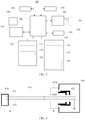
- FIG. 2 is a schematic structural diagram of a mobile phone 100 according to some embodiments.
- the mobile phone can support various applications such as a telephone application, an instant message transceiving application, a digital photographing and/or an image shooting application, a web browsing application, a music and/or video playing application, a video communication application, a social networking application, a financial application, a weather application, a shopping application, and an office application.
- applications such as a telephone application, an instant message transceiving application, a digital photographing and/or an image shooting application, a web browsing application, a music and/or video playing application, a video communication application, a social networking application, a financial application, a weather application, a shopping application, and an office application.
- FIG. 2 is a block diagram of a partial structure of a mobile phone 100 according to some embodiments.
- the mobile phone 100 includes parts such as an RF (Radio Frequency, radio frequency) circuit 110, a memory 120, an input unit 130, a display unit 140, a sensor 150, an audio frequency circuit 160, a USB port 170, a processor 180, and a power supply 190.
- RF Radio Frequency, radio frequency
- FIG. 2 is merely an example of an implementation, constitutes no limitation on the mobile phone, and may include more or fewer parts than those shown in the figure, or combine some parts, or have different part arrangements.
- the RF circuit 110 may be configured to: receive and send information, or receive and send a signal in a call process; in particular, after receiving downlink information from a base station, send the downlink information to the processor 180 for processing; and send related uplink data to the base station.
- the RF circuit usually includes but is not limited to an antenna, at least one amplifier, a transceiver, a coupler, an LNA (Low Noise Amplifier, low noise amplifier), and a duplexer.
- the RF circuit 110 may communicate with a network and another device through wireless communication.
- Any communications standard or protocol may be used for the wireless communication, including but not limited to GSM (Global System of Mobile communication, Global System for Mobile Communications), GPRS (General Packet Radio Service, general packet radio service), CDMA (Code Division Multiple Access, Code Division Multiple Access), WCDMA (Wideband Code Division Multiple Access, Wideband Code Division Multiple Access), LTE (Long Term Evolution, Long Term Evolution), an e-mail, and an SMS (Short Messaging Service, short message service).
- GSM Global System of Mobile communication, Global System for Mobile Communications
- GPRS General Packet Radio Service, general packet radio service
- CDMA Code Division Multiple Access, Code Division Multiple Access
- WCDMA Wideband Code Division Multiple Access
- LTE Long Term Evolution, Long Term Evolution
- an e-mail Long Term Evolution
- SMS Short Messaging Service
- the memory 120 may be configured to store a software program and a module, and the processor 180 performs various function applications of the mobile phone 100 and data processing by running the software program and the module stored in the memory 120.
- the memory 120 may mainly include a program storage area and a data storage area.
- the program storage area may store an operating system, an application program required by at least one function (such as a sound playing function or an image playing function), and the like.
- the data storage area may store data (such as audio data or a phone book) created based on use of the mobile phone 100, and the like.
- the memory 120 may include a high-speed random access memory, or may include a nonvolatile memory such as at least one magnetic disk storage device, a flash memory device, or another volatile solid-state storage device.
- the input unit 130 may be configured to receive entered digital or character information, and generate key signal or action signal input related to user setting and function control of the mobile phone 100.
- the input unit 130 may include one or more of a touch panel 131, a camera 132, and another input device 132.
- the touch panel 131 may be a touch display or a touchpad.
- the touch display is a device integrating a display and a touch area.
- the touchpad is a touch-sensitive area of a device that is different from the touch display and that does not display visual output.
- the touchpad may be a touch-sensitive surface separated from a display panel, or an extension part of a touch-sensitive surface including a touchscreen.
- the touch panel 131 may collect a touch operation performed by a user on or near the touch panel 131 (such as an operation performed by the user on the touch panel 131 or near the touch panel 131 by using any proper object or accessory, for example, a finger or a stylus), and drive a corresponding connection apparatus based on a preset program.
- the touch panel 131 may include two parts: a touch detection apparatus and a touch controller.
- the touch detection apparatus detects a touch location of the user, detects a signal brought by the touch operation, and transmits the signal to the touch controller.
- the touch controller receives touch information from the touch detection apparatus, converts the touch information into touch point coordinates, and sends the touch point coordinates to the processor 180.
- the touch controller can receive and execute a command sent by the processor 180.
- the touch panel 131 may be implemented in a plurality of types such as a resistive type, a capacitive type, an infrared ray type, and a surface acoustic wave type.
- the camera 132 may be one or more analog cameras, a digital camera, a depth camera, or a combination of any quantity of the foregoing cameras.
- the camera 132 may collect a video signal, and transmit the video signal to the processor 180, so that the processor 180 collects an input signal from the video signal (for example, identify a gesture operation of the user from the video signal).
- the input unit 130 may include the another input device 133.
- the another input device 133 may include but is not limited to one or more of a physical button board, a function key (such as a volume control key or an on/off key), a trackball, a mouse, a joystick, an electroencephalogram identifier, and a gyroscope.
- the input unit 130 may cover a microphone 162, the sensor 150, and the like.
- the microphone 162 may collect an audio signal, and transmit the audio signal to the processor, so that the processor collects an input signal from the audio signal (for example, identify a voice operation of the user from the audio signal).
- the display unit 140 may be configured to display information entered by the user or information provided for the user, and various menus of the mobile phone 100.
- the display unit 140 may include one or more of a display panel 141, a projection device 142, and another display device 143.
- the display panel 141 may be configured in a form of an LCD (Liquid Crystal Display, liquid crystal display), an OLED (Organic Light-Emitting Diode, organic light-emitting diode), or the like.
- the touch panel 131 may cover the display panel 141.
- the touch panel 131 When detecting a touch operation on or near the touch panel 131, the touch panel 131 transmits the touch operation to the processor 180 to determine a type of a touch event, and then the processor 180 provides corresponding visual output on the display panel 141 based on the type of the touch event.
- the touch panel 131 and the display panel 141 serve as two independent parts to implement input and input functions of the mobile phone 100. However, in some embodiments, the touch panel 131 and the display panel 141 may be integrated to implement the input and output functions of the mobile phone 100.
- the projection device 142 may be a mini projector or a 3D holographic projector.
- the mini projector may be a device that is installed on an intelligent glasses device and that projects, for imaging, an image on a retina of a human eye by using a translucent prism.
- the mini projector may be a device that projects an image on a display or a screen of the mobile phone for imaging.
- the 3D (three-dimensional) holographic projector is a device that may directly perform projection in physical space by using an interference and diffraction principle, to present a real three-dimensional image of an object.
- the display unit 140 may further include the another display device 142.
- the another display device 142 may include but is not limited to a display device (such as a TV) that is connected to the mobile phone in one or more connection manners such as a wireless local area network, a USB (Universal Serial Bus, Universal Serial Bus) data cable, and an HDMI (High Definition Multimedia Interface, high definition multimedia interface) cable.
- a display device such as a TV
- USB Universal Serial Bus
- HDMI High Definition Multimedia Interface, high definition multimedia interface
- the mobile phone 100 may further include at least one type of sensor 150, for example, a light sensor, a motion sensor, and another sensor.
- the light sensor may include an ambient light sensor and a proximity sensor.
- the ambient light sensor may adjust luminance of the display panel 141 based on brightness of ambient light.
- the proximity sensor may turn off the display panel 141 and/or backlight when the mobile phone 100 moves to an ear.
- an accelerometer sensor may detect a value of acceleration in each direction (generally, three axes), may detect a value and a direction of gravity in a static state, and may be configured to identify an application of a mobile phone posture (such as switching between a landscape and a portrait, a related game, and magnetometer posture calibration), a function related to vibration identification (such as a pedometer and a strike), and the like.
- Other sensors such as a gyroscope, a barometer, a hygrometer, a thermometer, and an infrared sensor may be further configured in the mobile phone 100, and details are not described herein.
- the audio frequency circuit 160, a loudspeaker 161, and the microphone 162 may provide an audio interface between the user and the mobile phone 100.
- the audio frequency circuit 160 may transmit, to the loudspeaker 161, an electrical signal obtained after received audio data is converted, and the loudspeaker 161 converts the electrical signal into a sound signal for output.
- the microphone 162 converts a collected sound signal into an electrical signal.
- the audio frequency circuit 160 converts the electrical signal into audio data after receiving the electrical signal, and then outputs the audio data to the processor 180 for processing.
- the processor 180 sends the audio data to, for example, another mobile phone by using the RF circuit 110, or outputs the audio data to the memory 120 for further processing.
- a universal serial bus (USB, Universal Serial Bus) port is configured to communicate with or charge an external device.
- the mobile phone 100 may perform data transmission with another USB device by using the USB port 170, or implement a charging function by using the USB port 170.
- the processor 180 is a control center of the mobile phone 100, is connected to each part of the entire mobile phone by using various interfaces and lines, and executes various functions of the mobile phone 100 and processes data by running or executing the software program and/or the module stored in the memory 120 and invoking data stored in the memory 120, so as to perform overall monitoring on the mobile phone.
- the processor 180 may include one or more processing units.
- the processor 180 may integrate an application processor and a modem processor.
- the application processor mainly processes an operating system, a user interface, an application program, and the like, and the modem processor mainly processes wireless communication. It can be understood that the foregoing modem processor may be not integrated into the processor 180.
- the mobile phone 100 further includes the power supply 190 (for example, a battery) that supplies power to each part.
- the power supply may be logically connected to the processor 180 by using a power management system, so as to implement functions such as charging management, discharging management, and power consumption management by using the power management system.
- the mobile phone 100 may have a housing (not shown).
- the housing may also be referred to as an enclosure, and may be made of any suitable material, including plastic, glass, ceramic, metal, another suitable material, or a combination of these materials.
- the housing or some parts of the housing may be formed by a dielectric material or another low-conductivity material, so that no interference is caused to a conductive antenna element located near the housing.
- the housing or some parts of the housing may also be made of a conducting material (such as metal).
- a conducting material such as metal.
- the mobile phone 100 may further include a camera, a Bluetooth module, and the like, and details are not described herein.
- a type of the USB port is not limited, and may include a USB type-C (USB Type-C) port, a USB type-A (USB Type-A) port, and a USB type-B (USB Type-B) port.
- USB Type-C USB Type-C
- USB Type-A USB type-A
- USB Type-B USB type-B
- FIG. 3 is a schematic diagram of connection between an electronic device and a charger by using a USB cable.
- An electronic device 320 is connected to a charger 310 by using a USB cable 330.
- the USB cable includes two ports: a USB port A and a USB port B, the USB port A of the USB cable 330 is connected to the charger 310, and the USB port B of the USB cable 330 is connected to a USB port of the electronic device.
- a metal housing 334b of the USB port B of the USB cable 330 is in contact with a metal housing 322 of the USB port of the electronic device, and a plastic housing 335b of the port B of the USB cable 330 is used to press against a housing of the electronic device 320, to fasten and protect the USB port B of the USB cable 330.
- the USB cable 330 includes a power cable 331, a ground cable 332, a data cable, and the like (not shown in the figure).
- the power cable 331 is connected to a power pin of the charger and a power pin of the USB port of the electronic device
- the ground cable 332 is connected to a ground pin of the charger and a ground pin of the USB port of the electronic device, so as to perform charging.
- the following describes a manner of fastening the metal housing 322 of the USB port of the electronic device 320 to a printed circuit board (printed circuit board, PCB) of the electronic device in an embodiment of the present invention.
- the metal housing 322 of the USB port is not connected to a ground of the PCB.
- the PCB usually has one or more cabling layers, for example, two cabling layers, four cabling layers, or six cabling layers.
- the cabling layers are isolated by using an insulation medium, and the insulation medium may be an FR-4 material.
- a line is disposed at the cabling layer, and the line is a tool used for component conduction, grounding, power supplying, and the like.
- the line is usually made of a metal conducting material such as copper foil or tin.
- Line layout may be performed at each cabling layer based on a design requirement of the electronic device. Lines located at different cabling layers may be connected based on a design requirement by using a via. For example, ground cables at the cabling layers may be connected by using a via.
- FIG. 4 is a schematic sectional view of a PCB according to an embodiment of the present invention.
- the PCB has a cabling layer 211, a cabling layer 212, a cabling layer 213, and a cabling layer 214, and the four cabling layers are isolated from each other by using insulation media 215.
- An area at the cabling layer excluding lines is an insulation medium, and the lines are isolated by using the insulation medium.
- At least one cabling layer on the PCB has a floating area.
- the floating area may be made of the same material, such as copper foil, as the line at the cabling layer.
- the floating area and another line at the same layer are isolated by using an insulation medium.
- a cabling layer adjacent to the cabling layer of the floating area has a metal area, and the metal area is opposite to the floating area.
- the metal area and an orthographic projection of the floating area on the cabling layer at which the metal area is located have an overlapping part.
- a plane of the cabling layer at which the metal area is located is used as a first plane, and the orthographic projection of the floating area on the cabling layer at which the metal area is located is a floating image obtained when a shape of the floating area is projected onto the first plane by using a set of light perpendicular to the first plane. That the metal area and the orthographic projection of the floating area on the cabling layer at which the metal area is located have an overlapping part means that the metal area and the floating image overlap on the first plane.
- the floating area is not connected to the metal area. To be specific, the floating area is not connected to the metal area because there is no conducting medium.
- the metal area may be the ground of the PCB, a power supply, or the like.
- a plurality of floating areas may be located at different cabling layers of the PCB, or a plurality of floating areas are located at one cabling layer of the PCB.
- a plurality of floating areas are located at one cabling layer of the PCB.
- a floating area may be disposed at the cabling layer 211, and a metal area opposite to the floating area is disposed at the cabling layer 212.
- a floating area may be disposed at the cabling layer 212, and a metal area opposite to the floating area may be disposed at the cabling layer 211 or the cabling layer 213.
- floating areas are respectively disposed at the cabling layer 211 and the cabling layer 214, and metal areas opposite to the floating areas may be disposed at the cabling layer 212 and the cabling layer 213.
- metal areas opposite to the floating areas may be respectively disposed at the cabling layer 211 and the cabling layer 214. If the two floating areas are opposite to each other (that is, an orthographic projection of a floating area at the cabling layer 212 on the cabling layer 213 and a floating area at the cabling layer 213 have an overlapping area), a distance d2 between the cabling layer 212 and the cabling layer 213 needs to be greater than a distance d1 between the cabling layer 211 and the cabling layer 212, and d2 also needs to be greater than a distance d3 between the cabling layer 213 and the cabling layer 214, so that the floating area and the metal area opposite to the floating area can form a capacitor. If the two floating areas are not opposite to each other, no requirement is imposed on d1, d2, and d3.
- One USB port is usually fastened to the PCB, and a metal housing of the USB port usually has two to four fixed contacts.
- a plurality of fixed contacts of the USB port may be connected to one metal floating area; or may be respectively connected to different floating areas located on a same cabling layer, where different fixed contacts may have different floating areas.
- the USB port may be fastened to the PCB in a surface mount manner, a pin fastening manner, or the like.
- the surface mount manner is: A fixed contact of the USB port is connected to a connection point of a fixed contact on a surface of the PCB in an adhering manner, and the connection point is a soldering joint.
- the plurality of floating areas may be connected by using a via.
- a connection point of the fixed contact is disposed on the PCB, and the connection point of the fixed contact is disposed in a floating area at a surface layer of the PCB, or is connected to the floating area of the PCB by using a via or through cabling. In this way, when the fixed contact of the USB port is connected to the connection point of the PCB, the fixed contact of the USB port may be connected to the plurality of floating areas.
- the pin fastening manner is: A fixed contact of the USB port is inserted into a connection point of the PCB, the connection point is a connection hole, the fixed contact is fastened to the connection hole through welding, and the connection hole passes through a plurality of cabling layers. In this manner, if one fixed contact of the USB port is connected to a plurality of floating areas located at different cabling layers of the PCB, the connection hole passes through the plurality of floating areas, the fixed contact is inserted into the connection hole to connect to the plurality of floating areas.
- a line at a cabling layer through which the connection hole passes and that has no floating area is isolated from the connection hole by using an insulation medium; or a line in a floating area at a cabling layer through which the connection hole passes is connected to the connection hole, and the connection hole is not connected to another line.
- some of the plurality of fixed contacts of the USB port are connected to a floating area of the PCB, and others may be connected to a soldering pad of the PCB.
- the soldering pad is isolated from all lines on the PCB by using an insulation medium.
- the floating area is disposed on the PCB
- the fixed contact of the metal housing of the USB port is connected to the floating area to form one electrode of a capacitor
- a metal area that is at an adjacent layer and that is opposite to the floating area form the other electrode of the capacitor, so as to form the capacitor on the PCB.
- the USB port is usually disposed at a lower part of the electronic device such as a mobile phone, and usually an antenna is also disposed at the lower part of the electronic device. When the USB port performs charging or data transmission, the antenna is interfered with.
- the capacitor on the PCB that is formed by using the floating area and the metal area that is at an adjacent layer and that is opposite to the floating area can prevent the antenna from being interfered with by the USB port.
- a plurality of capacitors C may be disposed. In other words, a plurality of floating areas are disposed.
- a value of the dielectric constant ⁇ is determined based on a material type of the insulation medium on the PCB
- s is an area of overlap of the floating area and the metal area
- the electrode distance d is specifically a spacing distance between the floating area and the metal area, that is, a distance between a cabling layer at which the floating area is located and a cabling layer at which the metal area is located. Therefore, an area of overlap of a floating area and a metal area opposite to the floating area on the PCB, a distance between cabling layers, and a material of an insulation medium may be designed based on required capacitance.
- the required capacitance is 33PF
- the distance between the layers of the PCB is 0.1 mm
- the insulation material is FR-4
- ⁇ of FR-4 is 4.2
- FIG. 5 is an implementation of connection between a USB port and a PCB in an electronic device according to an embodiment of the present invention.
- the PCB has a cabling layer 1 to a cabling layer 8 is used for description.
- the cabling layer 1 to the cabling layer 8 are mutually isolated by using insulation media 443.
- Each of the cabling layer 1 to the cabling layer 8 is disposed with a ground 441, and the grounds 441 are connected by using a via 442.
- Floating areas 444 may be disposed at cabling layers 1, 3, 5, and 7 on the PCB in a fixed area of the USB port that is connected to a fixed contact 326a of the USB port. Floating areas 444 may be disposed at cabling layers 1, 4, and 7 on a PCB area connected to a fixed contact 326b.
- FIG. 5 an example in which a line that is adjacent to the floating area 444 and that is at the same layer as the floating area 444 is a ground cable, and a metal area that is at an adjacent layer and that is opposite to the floating area 444 is a ground cable is used for description.
- the line that is adjacent to the floating area 444 and that is at the same layer as the floating area 444 or the metal area that is at an adjacent layer and that is opposite to the floating area 444 may also be a line outside the ground cable.
- the floating area 444 and the adjacent ground 441 at the same layer are isolated by using an insulation medium, and the floating area 444 and the ground at an adjacent layer are isolated by using an insulation medium, and are not connected.
- a ground is disposed in a metal area that is at an adjacent layer and that is opposite to the floating area 444, so as to implement better noise return.
- FIG. 5 shows two fixed contacts 326a and 326b of a metal housing 322 of the USB port.
- the metal housing 322 is fastened to the PCB 440 by using the fixed contacts 326a and 326b, and is in contact with the floating area 444 on the PCB 440.
- the PCB 440 in the electronic device is usually one PCB.
- FIG. 5 is a sectional view of a part, on a PCB, to which the USB port is fastened.
- FIG. 8 may also show a manner of fastening some fixed contacts of a USB port to a PCB.
- a fixed contact 326c is fastened to the PCB by using a via hole 745.
- the via hole 745 is not connected to the ground cable 441.
- the metal housing 322 of the USB port is not connected to a ground of the PCB 440.
- a current path: power pin -> perspiration -> metal housing of the USB port cannot be formed. Therefore, a case in which heat accumulates and the USB port is burned does not occur.
- FIG. 6a is a schematic diagram of a dotted line part 400 in FIG. 5 .
- the floating area 444 and the ground 441 at an adjacent cabling layer form a capacitor, and an area of overlap s is an area in which an orthographic projection of the floating area 444 on the adjacent cabling layer and the ground overlap.
- FIG. 6b is a possible implementation of FIG. 6a .
- the area of overlap s is obtained by subtracting a non-overlapping area 450 from an area of the floating area 444.
- FIG. 6c is another possible implementation of FIG. 6a .
- the area of overlap s is obtained by subtracting a non-overlapping area 451 from an area of the floating area 444.
- the non-overlapping area 451 may be ignored if the non-overlapping area 451 is small enough.
- An electrode distance d is a distance between the floating area 444 and the ground 441 (as shown in FIG. 6a ). Therefore, as shown in FIG. 6d , the capacitor is formed.
- FIG. 7 is a schematic diagram of cabling at a cabling layer on a PCB according to an embodiment of the present invention.
- a power pin soldering joint 661 for a USB port, data pin soldering joints 662 and 663, a ground soldering joint 664, floating areas 444, a ground 441, and another line 665 are disposed at one cabling layer. Other areas excluding these lines are insulation media 443.
- the floating area 444 is isolated from the adjacent ground cable 441, and the floating area 444 is isolated from the another line 665.
- the floating area 444 is disposed with cross-shaped cabling connected to a fixed contact of the USB port.
- the cross-shaped cabling may be replaced with star-shaped cabling, or may be cabling of another shape.
- FIG. 9 is another implementation of connection between a USB port and a PCB in an electronic device according to an embodiment of the present invention.
- the PCB has a cabling layer 1 to a cabling layer 6.
- a grid block is a floating area
- a gray block is another line
- floating areas are disposed at cabling layers 1,3, 4, and 5.
- a fixed contact 901 and a fixed contact 902 of the USB port may be connected to a same floating area (for example, a floating area at the cabling layer 1).
- a floating area at the cabling layer 4 is opposite to a floating area at the cabling layer 5.
- a distance between the cabling layer 4 and the cabling layer 5 is greater than a distance between the cabling layer 3 and the cabling layer 4, and is also greater than a distance between the cabling layer 5 and the cabling layer 6.
- FIG. 10 shows a charger and a USB cable in the prior art.
- a metal housing 612 of a USB port of a charger 610 is connected to a ground of the charger 610 by using a fixed contact.
- a USB cable 630 includes a power cable 631, a ground cable 632, a shielding cable 633, a data cable, and the like (not shown in the figure). Similar to descriptions of the power cable 331 and the ground cable 332, the power cable 631 and the ground cable 632 are used to connect an electronic device and the charger for charging.
- the data cable is used to transmit data.
- the shielding cable 633 and metal housings 634a and 634b of two USB ports of the USB cable 630 are pressed together, so that the shielding cable 633 is connected to the metal housings 634a and 634b. It can be learned that, when the USB port of the charger 610 is connected to a USB port A of the USB cable 630 in the prior art, the metal housing 612 of the USB port of the charger 610 is connected to the metal housing 634a of the USB port A of the USB cable. In this case, the shielding cable 633 is grounded, so that the metal housing 634b of a USB port B of the USB cable is grounded. When the USB port B of the USB cable 630 is connected to a USB port of the electronic device, a metal housing of the USB port of the electronic device is grounded. Consequently, a short circuit described in the background still occurs.
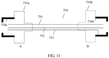
- FIG. 11 shows a USB cable according to an embodiment of the present invention.
- a USB cable 730 includes a power cable 731, a ground cable 732, a shielding cable 733, a data cable, and the like (not shown in the figure).
- the power cable 731 and the ground cable 732 are used to connect an electronic device and a charger for charging, and the data cable is used to transmit data.
- the shielding cable 733 is connected to a metal housing 734b of a USB port B of the USB cable 330, and the shielding cable 733 is not connected to a metal housing 734a of a USB port A of the USB cable.
- the USB port A of the USB cable 730 is connected to the USB port of the charger 610 in FIG. 10
- the USB port B of the USB cable 730 is connected to the USB port of the electronic device 320
- the shielding cable 733 of the USB cable is not connected to the metal housing of the USB port A on a side close to the USB port A
- the shielding cable 733 is not grounded even when the metal housing 612 of the USB port of the charger 610 is grounded. Therefore, the metal housing 322 of the USB port of the electronic device 320 is not grounded, so that a short circuit of the USB port of the electronic device can be prevented.
- both the metal housings of the USB port A and the USB port B of the USB cable may not be connected to the shielding cable.
- the USB port and the PCB in the charger may be connected in a manner shown in FIG. 5 and FIG. 9 .
- the USB port and the PCB in the charger may also be connected in a manner shown in FIG. 8 .
- the metal housing of the USB port in the charger is fastened to the PCB by using a fixed contact, and the fixed contact is not connected to the ground 4 of the PCB.
- the USB port and the PCB in the charger may also be connected by using a combination of manners in FIG. 5 / FIG. 9 and FIG. 8 .
- a charging system includes an electronic device, a charger, and a USB cable.
- the charger may be connected to the electronic device 320 in the foregoing embodiment by using a USB cable 630 or a USB cable 730, so as to resolve a short circuit problem of the USB port of the electronic device.
- a USB port and a PCB in the electronic device are connected in a manner shown in FIG. 5 or FIG. 9 , and the electronic device is used in conjunction with the USB cable 730, or in conjunction with the charger in which a USB port and a PCB are connected in a manner shown in FIG. 5 , FIG. 8 , or FIG. 9 . Therefore, the short circuit of the USB port of the electronic device can be resolved, and EMI interference to an antenna can be eliminated.
- the USB cable in this embodiment of the present invention may be further configured to transmit data between two electronic devices.
- the USB port B of the USB cable 730 is connected to the USB port of the electronic device 320, and the USB port A of the USB cable 730 is connected to a USB port of another electronic device.
- both the metal housings of the USB port A and the USB port B of the USB cable may not be connected to the shielding cable.
- the USB port and a PCB of the another electronic device may be connected in a manner of connecting the USB port and the PCB in the foregoing electronic device, for example, in a manner shown in FIG. 5 and FIG. 9 .
- FIG. 5 and FIG. 9 For details, refer to related descriptions in FIG. 5 and FIG. 9 . Details are not described herein again.
- a data transmission system includes a first electronic device, a second electronic device, and a USB cable.
- a USB port and a PCB in the first electronic device are connected in a manner shown in FIG. 5 or FIG. 9 , or by using a combination of manners in FIG. 5 / FIG. 9 and FIG. 8 .
- the USB cable is implemented in a manner shown in FIG. 11 .
- a USB port B is connected to the first electronic device, and a USB port A is connected to the second electronic device. There is no requirement imposed on a manner of connecting a USB port and a PCB of the second electronic device.
- the USB port and the PCB of the first electronic device and the second electronic device are connected in a manner shown in FIG. 5 or FIG. 9 , or by using a combination of manners in FIG. 5 / FIG. 9 and FIG. 8 , and no requirement is imposed on the USB cable.
Landscapes
- Engineering & Computer Science (AREA)
- Microelectronics & Electronic Packaging (AREA)
- General Engineering & Computer Science (AREA)
- Theoretical Computer Science (AREA)
- Physics & Mathematics (AREA)
- General Physics & Mathematics (AREA)
- Computer Hardware Design (AREA)
- Electromagnetism (AREA)
- Power Sources (AREA)
- Structures For Mounting Electric Components On Printed Circuit Boards (AREA)
- Combinations Of Printed Boards (AREA)
- Charge And Discharge Circuits For Batteries Or The Like (AREA)
- Parts Printed On Printed Circuit Boards (AREA)
- Coupling Device And Connection With Printed Circuit (AREA)
- Shielding Devices Or Components To Electric Or Magnetic Fields (AREA)
Description
- The present invention relates to the field of USB connection technologies, and in particular, to a device with a USB port.
- Currently, an electronic device such as a smartphone or a tablet personal computer performs charging, data transmission, and the like by using a USB port.
- Two or four fixed contacts 11 (as shown in
FIG. 1a ) are usually disposed on a metal housing of the universal serial bus (universal serial bus, USB) port on the electronic device, and the USB port on the electronic device is fastened to a printed circuit board (printed circuit board, PCB) of the electronic device by using thefixed contacts 11. The metal housing of the USB port is usually connected to a ground (as shown inFIG. 1b ) on the PCB of the electronic device by using thefixed contacts 11. Because the metal housing of the USB port is relatively close to a USB tongue, non-insulation materials such as perspiration and dust particles accumulate between the tongue and the metal housing of the USB port in daily use, especially between the USB housing and a power pin (VBUS) on the tongue (as shown inFIG. 1b ). After a high-voltage and high-current charger is connected, a state of a micro short circuit between a power supply and the ground is formed. The state cannot be detected by using an overcurrent detection mechanism of the electronic device. A current path: VBUS -> perspiration -> metal housing of the USB port exists, and heat accumulates on the USB port. Consequently, the USB port is burned, endangering user's safety. - The USB port is usually disposed at a lower part of the electronic device such as a mobile phone, and usually an antenna is also disposed at the lower part of the electronic device. When the USB port performs charging or data transmission, the antenna is interfered with. As shown in
FIG. 1c , currently the metal housing of the USB port is usually connected to the ground on the PCB of the electronic device by using an additional protection component. The protection component is configured to interference and prevent a micro short circuit. However, the protection component occupies internal space of the electronic device. Consequently, it is not conducive to lightening and thinning of the electronic device. -
EP0875963 discloses a filtered universal serial bus. The capacitive filter element 74 inEP0875963 has been identified as the printed circuit board. However it cannot be considered that the capacitive filter element comprises two cabling layers. The conductive plane 92 and the signal electrode 94 cannot be considered as cabling layers of the printed circuit board, since they are exclusively directed to provide the capacitor. -
EP1419559 relates to suppression of common electrical noise on the cable braid for the reduction of electromagnetic emissions in high-speed differential serial link cable connectors using technique applicable to the printed circuit board (PCB) on which this cable connector is mounted.The method involves providing a connector shell and connecting printed circuit board capacitor plates in a signal layer metallization (21,22,23,24) directly to the connector shell by means of connector pins 70 and providing low impedance alternating current path to logic ground layers (11,12,13). The high frequency low impedance alternating current path (2) comprises a plurality of metal plates in a plurality of signal layers (21, 22, 23, 24) forming a plurality of capacitor plates in parallel coupled between the connector shell (7) and a plurality of logic ground layers (11). The connector pins 60 connecting the connector outer shell to the various signal layer metallizations passes through multiple vias 51 through logic ground layer I and onto signal layer metallization 22 without making an electrical connection tologic ground 11. - Embodiments of the present invention provide an electronic device, a USB cable, and a charger, so that a short circuit of a USB port is prevented, interference of the USB port is shielded, and internal space of the electronic device is not occupied.
- An electronic device according to the invention is disclosed in
claim 1. Other aspects of the invention are disclosed in the dependent claims. - The metal housing of the USB port of the electronic device is not connected to the ground of the PCB, so that a short circuit does not occur. In addition, a floating area and a metal area opposite to the floating area are disposed on the PCB, and the metal housing of the USB port of the electronic device is connected to the floating area, so as to form a capacitor, thereby preventing an antenna from being interfered with by the USB port.
- With reference to the first aspect, in a first implementation of the first aspect, capacitance formed by the first floating area and the first metal area is

- With reference to the first aspect or the first implementation of the first aspect, in a second implementation of the first aspect, the PCB includes a second floating area, the second floating area is located at the first cabling layer, the second cabling layer has a second metal area, an orthographic projection of the second floating area on the second cabling layer and the second metal area have an overlapping area, and the second floating area is not connected to the second metal area; and the plurality of fixed contacts of the USB port include a second fixed contact, the second fixed contact is connected to the second floating area, and the second fixed contact is not connected to the second metal area.
- With reference to the first aspect or the first implementation of the first aspect, in a third implementation of the first aspect, a third cabling layer in the at least two cabling layers include a third floating area, a fourth cabling layer in the at least two cabling layers and the third cabling layer are adjacent and isolated by using the insulation medium, the fourth cabling layer is disposed with a third metal area, an orthographic projection of the third floating area on the fourth cabling layer and the third metal area have an overlapping area, and the third floating area is not connected to the third metal area; and the first fixed contact is connected to the first floating area and the third floating area, and the first fixed contact is not connected to the first metal area and the third metal area.
- With reference to the third implementation of the first aspect, in a fourth implementation of the first aspect, the first cabling layer is not adjacent to the third cabling layer. Optionally, a distance between the first cabling layer and the third cabling layer is greater than a distance between the first cabling layer and the second cabling layer, and is greater than a distance between the third cabling layer and the fourth cabling layer.
- With reference to any one of the first aspect or the first to the fourth implementations of the first aspect, the first metal area is the ground of the PCB. Therefore, noise backflow can be better implemented.
- A second aspect provides that the electronic device is a charger.
-
-
FIG. 1a is a schematic diagram of a USB port in the prior art; -
FIG. 1b is a schematic diagram of a micro short circuit in a USB port in the prior art; -
FIG. 1c is a schematic diagram in which a USB port is connected to a PCB by using a protection component in the prior art; -
FIG. 2 is a schematic diagram of an architecture of a mobile phone according to an embodiment of the present invention; -
FIG. 3 is a schematic diagram of connection between a USB port on an electronic device and a charger by using a USB cable according to an embodiment of the present invention; -
FIG. 4 is a schematic sectional view of a PCB according to an embodiment of the present invention; -
FIG. 5 is a schematic diagram of connection between a USB port on an electronic device and a PCB according to an embodiment of the present invention; -
FIG. 6a is a schematic partial view of adotted line box 400 inFIG. 5 ; -
FIG. 6b is a front view of an implementation corresponding toFIG. 6a ; -
FIG. 6c is a front view of another implementation corresponding toFIG. 6a ; -
FIG. 6d is an equivalent schematic diagram of a circuit inFIG. 6a ; -
FIG. 7 is a front view of a PCB according to an embodiment of the present invention; -
FIG. 8 is another schematic diagram of connection between a fixed contact of a USB port on an electronic device and a PCB according to an embodiment of the present invention; -
FIG. 9 is still another schematic diagram of connection between a fixed contact of a USB port on an electronic device and a PCB according to an embodiment of the present invention; -
FIG. 10 is a schematic diagram of a USB cable in the prior art; and -
FIG. 11 is a schematic diagram of a USB cable according to an embodiment of the present invention. - To make the purpose, technical solutions, and advantages of the embodiments of the present invention clearer, the following describes the technical solutions of the embodiments of the present invention with reference to the accompanying drawings in the embodiments of the present invention.
- An electronic device may be a mobile phone (also referred to as a smartphone), a tablet personal computer (Tablet Personal Computer), a personal digital assistant (personal digital assistant, PDA for short), an e-book reader (English: e-book reader) or a wearable device (Wearable Device), a virtual reality interactive device (Virtual Reality Interactive Device), or the like. The electronic device may establish communication with a network by using a 2G (second generation mobile phone communications technical specification), a 3G (third generation mobile phone communications technical specification), a 4G (fourth generation mobile phone communications technical specification), a 5G (fifth generation mobile phone communications technical specification), a W-LAN (wireless local area network), or a possible communication mode in the future.
- For ease of description, a structure of the electronic device is described by using a mobile phone as an example.
-
FIG. 2 is a schematic structural diagram of amobile phone 100 according to some embodiments. The mobile phone can support various applications such as a telephone application, an instant message transceiving application, a digital photographing and/or an image shooting application, a web browsing application, a music and/or video playing application, a video communication application, a social networking application, a financial application, a weather application, a shopping application, and an office application. -
FIG. 2 is a block diagram of a partial structure of amobile phone 100 according to some embodiments. Referring toFIG. 2 , themobile phone 100 includes parts such as an RF (Radio Frequency, radio frequency) circuit 110, amemory 120, aninput unit 130, adisplay unit 140, asensor 150, anaudio frequency circuit 160, aUSB port 170, aprocessor 180, and apower supply 190. - A person skilled in the art may understand that the structure of the mobile phone shown in
FIG. 2 is merely an example of an implementation, constitutes no limitation on the mobile phone, and may include more or fewer parts than those shown in the figure, or combine some parts, or have different part arrangements. - The following specifically describes each component of the
mobile phone 100 with reference toFIG. 2 . - The RF circuit 110 may be configured to: receive and send information, or receive and send a signal in a call process; in particular, after receiving downlink information from a base station, send the downlink information to the
processor 180 for processing; and send related uplink data to the base station. The RF circuit usually includes but is not limited to an antenna, at least one amplifier, a transceiver, a coupler, an LNA (Low Noise Amplifier, low noise amplifier), and a duplexer. In addition, the RF circuit 110 may communicate with a network and another device through wireless communication. Any communications standard or protocol may be used for the wireless communication, including but not limited to GSM (Global System of Mobile communication, Global System for Mobile Communications), GPRS (General Packet Radio Service, general packet radio service), CDMA (Code Division Multiple Access, Code Division Multiple Access), WCDMA (Wideband Code Division Multiple Access, Wideband Code Division Multiple Access), LTE (Long Term Evolution, Long Term Evolution), an e-mail, and an SMS (Short Messaging Service, short message service). - The
memory 120 may be configured to store a software program and a module, and theprocessor 180 performs various function applications of themobile phone 100 and data processing by running the software program and the module stored in thememory 120. Thememory 120 may mainly include a program storage area and a data storage area. The program storage area may store an operating system, an application program required by at least one function (such as a sound playing function or an image playing function), and the like. The data storage area may store data (such as audio data or a phone book) created based on use of themobile phone 100, and the like. In addition, thememory 120 may include a high-speed random access memory, or may include a nonvolatile memory such as at least one magnetic disk storage device, a flash memory device, or another volatile solid-state storage device. - The
input unit 130 may be configured to receive entered digital or character information, and generate key signal or action signal input related to user setting and function control of themobile phone 100. Specifically, theinput unit 130 may include one or more of atouch panel 131, acamera 132, and anotherinput device 132. Thetouch panel 131 may be a touch display or a touchpad. The touch display is a device integrating a display and a touch area. The touchpad is a touch-sensitive area of a device that is different from the touch display and that does not display visual output. The touchpad may be a touch-sensitive surface separated from a display panel, or an extension part of a touch-sensitive surface including a touchscreen. Thetouch panel 131 may collect a touch operation performed by a user on or near the touch panel 131 (such as an operation performed by the user on thetouch panel 131 or near thetouch panel 131 by using any proper object or accessory, for example, a finger or a stylus), and drive a corresponding connection apparatus based on a preset program. Optionally, thetouch panel 131 may include two parts: a touch detection apparatus and a touch controller. The touch detection apparatus detects a touch location of the user, detects a signal brought by the touch operation, and transmits the signal to the touch controller. The touch controller receives touch information from the touch detection apparatus, converts the touch information into touch point coordinates, and sends the touch point coordinates to theprocessor 180. In addition, the touch controller can receive and execute a command sent by theprocessor 180. In addition, thetouch panel 131 may be implemented in a plurality of types such as a resistive type, a capacitive type, an infrared ray type, and a surface acoustic wave type. Thecamera 132 may be one or more analog cameras, a digital camera, a depth camera, or a combination of any quantity of the foregoing cameras. Thecamera 132 may collect a video signal, and transmit the video signal to theprocessor 180, so that theprocessor 180 collects an input signal from the video signal (for example, identify a gesture operation of the user from the video signal). In addition to thetouch panel 131 and thecamera 132, theinput unit 130 may include the anotherinput device 133. Specifically, the anotherinput device 133 may include but is not limited to one or more of a physical button board, a function key (such as a volume control key or an on/off key), a trackball, a mouse, a joystick, an electroencephalogram identifier, and a gyroscope. In addition, theinput unit 130 may cover amicrophone 162, thesensor 150, and the like. In some embodiments, themicrophone 162 may collect an audio signal, and transmit the audio signal to the processor, so that the processor collects an input signal from the audio signal (for example, identify a voice operation of the user from the audio signal). - The
display unit 140 may be configured to display information entered by the user or information provided for the user, and various menus of themobile phone 100. Thedisplay unit 140 may include one or more of adisplay panel 141, aprojection device 142, and anotherdisplay device 143. Optionally, thedisplay panel 141 may be configured in a form of an LCD (Liquid Crystal Display, liquid crystal display), an OLED (Organic Light-Emitting Diode, organic light-emitting diode), or the like. Further, thetouch panel 131 may cover thedisplay panel 141. When detecting a touch operation on or near thetouch panel 131, thetouch panel 131 transmits the touch operation to theprocessor 180 to determine a type of a touch event, and then theprocessor 180 provides corresponding visual output on thedisplay panel 141 based on the type of the touch event. InFIG. 2 , thetouch panel 131 and thedisplay panel 141 serve as two independent parts to implement input and input functions of themobile phone 100. However, in some embodiments, thetouch panel 131 and thedisplay panel 141 may be integrated to implement the input and output functions of themobile phone 100. Theprojection device 142 may be a mini projector or a 3D holographic projector. The mini projector may be a device that is installed on an intelligent glasses device and that projects, for imaging, an image on a retina of a human eye by using a translucent prism. Alternatively, the mini projector may be a device that projects an image on a display or a screen of the mobile phone for imaging. The 3D (three-dimensional) holographic projector is a device that may directly perform projection in physical space by using an interference and diffraction principle, to present a real three-dimensional image of an object. In addition to thedisplay panel 141 and theprojection device 142, thedisplay unit 140 may further include the anotherdisplay device 142. Specifically, the anotherdisplay device 142 may include but is not limited to a display device (such as a TV) that is connected to the mobile phone in one or more connection manners such as a wireless local area network, a USB (Universal Serial Bus, Universal Serial Bus) data cable, and an HDMI (High Definition Multimedia Interface, high definition multimedia interface) cable. - The
mobile phone 100 may further include at least one type ofsensor 150, for example, a light sensor, a motion sensor, and another sensor. Specifically, the light sensor may include an ambient light sensor and a proximity sensor. The ambient light sensor may adjust luminance of thedisplay panel 141 based on brightness of ambient light. The proximity sensor may turn off thedisplay panel 141 and/or backlight when themobile phone 100 moves to an ear. As a motion sensor, an accelerometer sensor may detect a value of acceleration in each direction (generally, three axes), may detect a value and a direction of gravity in a static state, and may be configured to identify an application of a mobile phone posture (such as switching between a landscape and a portrait, a related game, and magnetometer posture calibration), a function related to vibration identification (such as a pedometer and a strike), and the like. Other sensors such as a gyroscope, a barometer, a hygrometer, a thermometer, and an infrared sensor may be further configured in themobile phone 100, and details are not described herein. - The
audio frequency circuit 160, aloudspeaker 161, and themicrophone 162 may provide an audio interface between the user and themobile phone 100. Theaudio frequency circuit 160 may transmit, to theloudspeaker 161, an electrical signal obtained after received audio data is converted, and theloudspeaker 161 converts the electrical signal into a sound signal for output. In addition, themicrophone 162 converts a collected sound signal into an electrical signal. Theaudio frequency circuit 160 converts the electrical signal into audio data after receiving the electrical signal, and then outputs the audio data to theprocessor 180 for processing. Theprocessor 180 sends the audio data to, for example, another mobile phone by using the RF circuit 110, or outputs the audio data to thememory 120 for further processing. - A universal serial bus (USB, Universal Serial Bus) port is configured to communicate with or charge an external device. The
mobile phone 100 may perform data transmission with another USB device by using theUSB port 170, or implement a charging function by using theUSB port 170. - The
processor 180 is a control center of themobile phone 100, is connected to each part of the entire mobile phone by using various interfaces and lines, and executes various functions of themobile phone 100 and processes data by running or executing the software program and/or the module stored in thememory 120 and invoking data stored in thememory 120, so as to perform overall monitoring on the mobile phone. Optionally, theprocessor 180 may include one or more processing units. Preferably, theprocessor 180 may integrate an application processor and a modem processor. The application processor mainly processes an operating system, a user interface, an application program, and the like, and the modem processor mainly processes wireless communication. It can be understood that the foregoing modem processor may be not integrated into theprocessor 180. - The
mobile phone 100 further includes the power supply 190 (for example, a battery) that supplies power to each part. Preferably, the power supply may be logically connected to theprocessor 180 by using a power management system, so as to implement functions such as charging management, discharging management, and power consumption management by using the power management system. - The
mobile phone 100 may have a housing (not shown). The housing may also be referred to as an enclosure, and may be made of any suitable material, including plastic, glass, ceramic, metal, another suitable material, or a combination of these materials. In some implementations, the housing or some parts of the housing may be formed by a dielectric material or another low-conductivity material, so that no interference is caused to a conductive antenna element located near the housing. The housing or some parts of the housing may also be made of a conducting material (such as metal). When the housing is made of a metal element, one or more metal elements may be used as a part of an antenna in themobile phone 100, such as a radiator or a ground. - Although not shown in the figure, the
mobile phone 100 may further include a camera, a Bluetooth module, and the like, and details are not described herein. - In this embodiment of the present invention, a type of the USB port is not limited, and may include a USB type-C (USB Type-C) port, a USB type-A (USB Type-A) port, and a USB type-B (USB Type-B) port.
-
FIG. 3 is a schematic diagram of connection between an electronic device and a charger by using a USB cable. Anelectronic device 320 is connected to acharger 310 by using aUSB cable 330. - In
FIG. 3 , the USB cable includes two ports: a USB port A and a USB port B, the USB port A of theUSB cable 330 is connected to thecharger 310, and the USB port B of theUSB cable 330 is connected to a USB port of the electronic device. Ametal housing 334b of the USB port B of theUSB cable 330 is in contact with ametal housing 322 of the USB port of the electronic device, and aplastic housing 335b of the port B of theUSB cable 330 is used to press against a housing of theelectronic device 320, to fasten and protect the USB port B of theUSB cable 330. TheUSB cable 330 includes apower cable 331, aground cable 332, a data cable, and the like (not shown in the figure). Thepower cable 331 is connected to a power pin of the charger and a power pin of the USB port of the electronic device, and theground cable 332 is connected to a ground pin of the charger and a ground pin of the USB port of the electronic device, so as to perform charging. - The following describes a manner of fastening the
metal housing 322 of the USB port of theelectronic device 320 to a printed circuit board (printed circuit board, PCB) of the electronic device in an embodiment of the present invention. In this embodiment, themetal housing 322 of the USB port is not connected to a ground of the PCB. - The PCB usually has one or more cabling layers, for example, two cabling layers, four cabling layers, or six cabling layers. The cabling layers are isolated by using an insulation medium, and the insulation medium may be an FR-4 material. A line is disposed at the cabling layer, and the line is a tool used for component conduction, grounding, power supplying, and the like. The line is usually made of a metal conducting material such as copper foil or tin. Line layout may be performed at each cabling layer based on a design requirement of the electronic device. Lines located at different cabling layers may be connected based on a design requirement by using a via. For example, ground cables at the cabling layers may be connected by using a via. The PCB in this embodiment of the present invention has at least two cabling layers.
FIG. 4 is a schematic sectional view of a PCB according to an embodiment of the present invention. The PCB has acabling layer 211, acabling layer 212, acabling layer 213, and acabling layer 214, and the four cabling layers are isolated from each other by usinginsulation media 215. An area at the cabling layer excluding lines is an insulation medium, and the lines are isolated by using the insulation medium. - At least one cabling layer on the PCB has a floating area. The floating area may be made of the same material, such as copper foil, as the line at the cabling layer. The floating area and another line at the same layer are isolated by using an insulation medium. A cabling layer adjacent to the cabling layer of the floating area has a metal area, and the metal area is opposite to the floating area. To be specific, the metal area and an orthographic projection of the floating area on the cabling layer at which the metal area is located have an overlapping part. A plane of the cabling layer at which the metal area is located is used as a first plane, and the orthographic projection of the floating area on the cabling layer at which the metal area is located is a floating image obtained when a shape of the floating area is projected onto the first plane by using a set of light perpendicular to the first plane. That the metal area and the orthographic projection of the floating area on the cabling layer at which the metal area is located have an overlapping part means that the metal area and the floating image overlap on the first plane. The floating area is not connected to the metal area. To be specific, the floating area is not connected to the metal area because there is no conducting medium. The metal area may be the ground of the PCB, a power supply, or the like.
- A plurality of floating areas may be located at different cabling layers of the PCB, or a plurality of floating areas are located at one cabling layer of the PCB. When two floating areas located at different cabling layers are opposite to each other, and distances between cabling layers are the same, there is a cabling layer between the two floating areas. In other words, the cabling layers at which the plurality of floating areas are located are not adjacent.
- Referring to
FIG. 4 , a floating area may be disposed at thecabling layer 211, and a metal area opposite to the floating area is disposed at thecabling layer 212. Alternatively, a floating area may be disposed at thecabling layer 212, and a metal area opposite to the floating area may be disposed at thecabling layer 211 or thecabling layer 213. There may be a plurality of floating areas. For example, floating areas are respectively disposed at thecabling layer 211 and thecabling layer 214, and metal areas opposite to the floating areas may be disposed at thecabling layer 212 and thecabling layer 213. If floating areas are respectively disposed at thecabling layer 212 and thecabling layer 213, metal areas opposite to the floating areas may be respectively disposed at thecabling layer 211 and thecabling layer 214. If the two floating areas are opposite to each other (that is, an orthographic projection of a floating area at thecabling layer 212 on thecabling layer 213 and a floating area at thecabling layer 213 have an overlapping area), a distance d2 between thecabling layer 212 and thecabling layer 213 needs to be greater than a distance d1 between thecabling layer 211 and thecabling layer 212, and d2 also needs to be greater than a distance d3 between thecabling layer 213 and thecabling layer 214, so that the floating area and the metal area opposite to the floating area can form a capacitor. If the two floating areas are not opposite to each other, no requirement is imposed on d1, d2, and d3. - One USB port is usually fastened to the PCB, and a metal housing of the USB port usually has two to four fixed contacts. A plurality of fixed contacts of the USB port may be connected to one metal floating area; or may be respectively connected to different floating areas located on a same cabling layer, where different fixed contacts may have different floating areas.
- The USB port may be fastened to the PCB in a surface mount manner, a pin fastening manner, or the like.
- The surface mount manner is: A fixed contact of the USB port is connected to a connection point of a fixed contact on a surface of the PCB in an adhering manner, and the connection point is a soldering joint. In this manner, if one fixed contact of the USB port is connected to a plurality of floating areas located at different cabling layers of the PCB, the plurality of floating areas may be connected by using a via. A connection point of the fixed contact is disposed on the PCB, and the connection point of the fixed contact is disposed in a floating area at a surface layer of the PCB, or is connected to the floating area of the PCB by using a via or through cabling. In this way, when the fixed contact of the USB port is connected to the connection point of the PCB, the fixed contact of the USB port may be connected to the plurality of floating areas.
- The pin fastening manner is: A fixed contact of the USB port is inserted into a connection point of the PCB, the connection point is a connection hole, the fixed contact is fastened to the connection hole through welding, and the connection hole passes through a plurality of cabling layers. In this manner, if one fixed contact of the USB port is connected to a plurality of floating areas located at different cabling layers of the PCB, the connection hole passes through the plurality of floating areas, the fixed contact is inserted into the connection hole to connect to the plurality of floating areas. A line at a cabling layer through which the connection hole passes and that has no floating area is isolated from the connection hole by using an insulation medium; or a line in a floating area at a cabling layer through which the connection hole passes is connected to the connection hole, and the connection hole is not connected to another line.
- Based on a circuit configuration requirement, some of the plurality of fixed contacts of the USB port are connected to a floating area of the PCB, and others may be connected to a soldering pad of the PCB. The soldering pad is isolated from all lines on the PCB by using an insulation medium.
- In this embodiment of the present invention, the floating area is disposed on the PCB, the fixed contact of the metal housing of the USB port is connected to the floating area to form one electrode of a capacitor, and a metal area that is at an adjacent layer and that is opposite to the floating area form the other electrode of the capacitor, so as to form the capacitor on the PCB. The USB port is usually disposed at a lower part of the electronic device such as a mobile phone, and usually an antenna is also disposed at the lower part of the electronic device. When the USB port performs charging or data transmission, the antenna is interfered with. The capacitor on the PCB that is formed by using the floating area and the metal area that is at an adjacent layer and that is opposite to the floating area can prevent the antenna from being interfered with by the USB port.
- Specifically, a relationship between capacitance and an interfering frequency F is

- The capacitance C may be further calculated based on a formula

- Capacitance formed by two metal plates that are opposite to each other and that are connected to different electrodes may be obtained through calculation based on a calculation formula

- As shown in
FIG. 5, FIG. 5 is an implementation of connection between a USB port and a PCB in an electronic device according to an embodiment of the present invention. InFIG. 5 , an example in which the PCB has acabling layer 1 to acabling layer 8 is used for description. Thecabling layer 1 to thecabling layer 8 are mutually isolated by usinginsulation media 443. Each of thecabling layer 1 to thecabling layer 8 is disposed with aground 441, and thegrounds 441 are connected by using a via 442. - Floating
areas 444 may be disposed atcabling layers contact 326a of the USB port. Floatingareas 444 may be disposed atcabling layers fixed contact 326b. InFIG. 5 , an example in which a line that is adjacent to the floatingarea 444 and that is at the same layer as the floatingarea 444 is a ground cable, and a metal area that is at an adjacent layer and that is opposite to the floatingarea 444 is a ground cable is used for description. In an actual product, the line that is adjacent to the floatingarea 444 and that is at the same layer as the floatingarea 444 or the metal area that is at an adjacent layer and that is opposite to the floatingarea 444 may also be a line outside the ground cable. InFIG. 5 , the floatingarea 444 and theadjacent ground 441 at the same layer are isolated by using an insulation medium, and the floatingarea 444 and the ground at an adjacent layer are isolated by using an insulation medium, and are not connected. A ground is disposed in a metal area that is at an adjacent layer and that is opposite to the floatingarea 444, so as to implement better noise return. -
FIG. 5 shows two fixedcontacts metal housing 322 of the USB port. Themetal housing 322 is fastened to thePCB 440 by using the fixedcontacts area 444 on thePCB 440. ThePCB 440 in the electronic device is usually one PCB.FIG. 5 is a sectional view of a part, on a PCB, to which the USB port is fastened. -
FIG. 8 may also show a manner of fastening some fixed contacts of a USB port to a PCB. Afixed contact 326c is fastened to the PCB by using a viahole 745. The viahole 745 is not connected to theground cable 441. - The
metal housing 322 of the USB port is not connected to a ground of thePCB 440. When charging is performed by using the USB port, a current path: power pin -> perspiration -> metal housing of the USB port cannot be formed. Therefore, a case in which heat accumulates and the USB port is burned does not occur. - As shown in
FIG. 6a, FIG. 6a is a schematic diagram of a dottedline part 400 inFIG. 5 . The floatingarea 444 and theground 441 at an adjacent cabling layer form a capacitor, and an area of overlap s is an area in which an orthographic projection of the floatingarea 444 on the adjacent cabling layer and the ground overlap. As shown inFIG. 6b, FIG. 6b is a possible implementation ofFIG. 6a . The area of overlap s is obtained by subtracting anon-overlapping area 450 from an area of the floatingarea 444. As shown inFIG. 6c, FIG. 6c is another possible implementation ofFIG. 6a . The area of overlap s is obtained by subtracting anon-overlapping area 451 from an area of the floatingarea 444. Thenon-overlapping area 451 may be ignored if thenon-overlapping area 451 is small enough. An electrode distance d is a distance between the floatingarea 444 and the ground 441 (as shown inFIG. 6a ). Therefore, as shown inFIG. 6d , the capacitor is formed. - As shown in
FIG. 7, FIG. 7 is a schematic diagram of cabling at a cabling layer on a PCB according to an embodiment of the present invention. A power pin soldering joint 661 for a USB port, datapin soldering joints areas 444, aground 441, and anotherline 665 are disposed at one cabling layer. Other areas excluding these lines areinsulation media 443. The floatingarea 444 is isolated from theadjacent ground cable 441, and the floatingarea 444 is isolated from the anotherline 665. The floatingarea 444 is disposed with cross-shaped cabling connected to a fixed contact of the USB port. The cross-shaped cabling may be replaced with star-shaped cabling, or may be cabling of another shape. -
FIG. 9 is another implementation of connection between a USB port and a PCB in an electronic device according to an embodiment of the present invention. The PCB has acabling layer 1 to acabling layer 6. InFIG. 9 , a grid block is a floating area, a gray block is another line, and floating areas are disposed atcabling layers fixed contact 901 and afixed contact 902 of the USB port may be connected to a same floating area (for example, a floating area at the cabling layer 1). A floating area at thecabling layer 4 is opposite to a floating area at thecabling layer 5. A distance between thecabling layer 4 and thecabling layer 5 is greater than a distance between thecabling layer 3 and thecabling layer 4, and is also greater than a distance between thecabling layer 5 and thecabling layer 6. - The foregoing describes an implementation of fastening the USB port of the electronic device to the PCB in the embodiments of the present invention. To prevent a short circuit of the USB port, a corresponding USB cable or charger is required.
-
FIG. 10 shows a charger and a USB cable in the prior art. Ametal housing 612 of a USB port of acharger 610 is connected to a ground of thecharger 610 by using a fixed contact. AUSB cable 630 includes apower cable 631, aground cable 632, a shieldingcable 633, a data cable, and the like (not shown in the figure). Similar to descriptions of thepower cable 331 and theground cable 332, thepower cable 631 and theground cable 632 are used to connect an electronic device and the charger for charging. The data cable is used to transmit data. During manufacturing, the shieldingcable 633 andmetal housings USB cable 630 are pressed together, so that the shieldingcable 633 is connected to themetal housings charger 610 is connected to a USB port A of theUSB cable 630 in the prior art, themetal housing 612 of the USB port of thecharger 610 is connected to themetal housing 634a of the USB port A of the USB cable. In this case, the shieldingcable 633 is grounded, so that themetal housing 634b of a USB port B of the USB cable is grounded. When the USB port B of theUSB cable 630 is connected to a USB port of the electronic device, a metal housing of the USB port of the electronic device is grounded. Consequently, a short circuit described in the background still occurs. -
FIG. 11 shows a USB cable according to an embodiment of the present invention. AUSB cable 730 includes apower cable 731, aground cable 732, a shieldingcable 733, a data cable, and the like (not shown in the figure). Thepower cable 731 and theground cable 732 are used to connect an electronic device and a charger for charging, and the data cable is used to transmit data. The shieldingcable 733 is connected to ametal housing 734b of a USB port B of theUSB cable 330, and the shieldingcable 733 is not connected to ametal housing 734a of a USB port A of the USB cable. - When the USB port A of the
USB cable 730 is connected to the USB port of thecharger 610 inFIG. 10 , and the USB port B of theUSB cable 730 is connected to the USB port of theelectronic device 320, because the shieldingcable 733 of the USB cable is not connected to the metal housing of the USB port A on a side close to the USB port A, the shieldingcable 733 is not grounded even when themetal housing 612 of the USB port of thecharger 610 is grounded. Therefore, themetal housing 322 of the USB port of theelectronic device 320 is not grounded, so that a short circuit of the USB port of the electronic device can be prevented. - Optionally, both the metal housings of the USB port A and the USB port B of the USB cable may not be connected to the shielding cable.
- Optionally, the USB port and the PCB in the charger may be connected in a manner shown in
FIG. 5 andFIG. 9 . For details, refer to related descriptions inFIG. 5 andFIG. 9 . Details are not described herein again. Optionally, the USB port and the PCB in the charger may also be connected in a manner shown inFIG. 8 . The metal housing of the USB port in the charger is fastened to the PCB by using a fixed contact, and the fixed contact is not connected to theground 4 of the PCB. The USB port and the PCB in the charger may also be connected by using a combination of manners inFIG. 5 /FIG. 9 andFIG. 8 . - A charging system includes an electronic device, a charger, and a USB cable. When a USB port and a PCB in the charger are connected in a manner shown in
FIG. 5 /FIG. 9 or in a manner shown inFIG. 8 , the charger may be connected to theelectronic device 320 in the foregoing embodiment by using aUSB cable 630 or aUSB cable 730, so as to resolve a short circuit problem of the USB port of the electronic device. A USB port and a PCB in the electronic device are connected in a manner shown inFIG. 5 orFIG. 9 , and the electronic device is used in conjunction with theUSB cable 730, or in conjunction with the charger in which a USB port and a PCB are connected in a manner shown inFIG. 5 ,FIG. 8 , orFIG. 9 . Therefore, the short circuit of the USB port of the electronic device can be resolved, and EMI interference to an antenna can be eliminated. - The USB cable in this embodiment of the present invention may be further configured to transmit data between two electronic devices. For the USB cable, refer to
FIG. 11 . The USB port B of theUSB cable 730 is connected to the USB port of theelectronic device 320, and the USB port A of theUSB cable 730 is connected to a USB port of another electronic device. Optionally, both the metal housings of the USB port A and the USB port B of the USB cable may not be connected to the shielding cable. - Optionally, the USB port and a PCB of the another electronic device may be connected in a manner of connecting the USB port and the PCB in the foregoing electronic device, for example, in a manner shown in
FIG. 5 andFIG. 9 . For details, refer to related descriptions inFIG. 5 andFIG. 9 . Details are not described herein again. - A data transmission system includes a first electronic device, a second electronic device, and a USB cable. In a first optional manner, a USB port and a PCB in the first electronic device are connected in a manner shown in
FIG. 5 orFIG. 9 , or by using a combination of manners inFIG. 5 /FIG. 9 andFIG. 8 . The USB cable is implemented in a manner shown inFIG. 11 . A USB port B is connected to the first electronic device, and a USB port A is connected to the second electronic device. There is no requirement imposed on a manner of connecting a USB port and a PCB of the second electronic device. In a second optional manner, the USB port and the PCB of the first electronic device and the second electronic device are connected in a manner shown inFIG. 5 orFIG. 9 , or by using a combination of manners inFIG. 5 /FIG. 9 andFIG. 8 , and no requirement is imposed on the USB cable.
Claims (11)
- An electronic device (320), wherein the electronic device comprises a universal serial bus (universal serial bus, USB) port and a printed circuit board;the printed circuit board has at least two cabling layers (211, 212), a first cabling layer (211) in the at least two cabling layers has a first floating area (444) and a line (665) outside the first floating area (444), there is an insulation medium (443) between the first floating area (444) and the line (665) outside the first floating area (444), a second cabling layer (212) in the at least two cabling layers and the first cabling layer (211) are adjacent and isolated by using an insulation material (215), the second cabling layer (212) has a first metal area, an orthographic projection of the first floating area (444) on the second cabling layer (212) and the first metal area have an overlapping area, and the first floating area (444) is not connected to the first metal area; anda metal housing (322) of the USB port has a plurality of fixed contacts (326), the plurality of fixed contacts (326) are fastened to the printed circuit board, the plurality of fixed contacts (326) are not connected to a ground (441) of the printed circuit board, the plurality of fixed contacts (326) comprise a first fixed contact (326a), the first fixed contact (326a) is connected to the first floating area (444), and the first fixed contact (326a) is not connected to the first metal area.
- The electronic device (326) according to claim 1, wherein capacitance formed by the first floating area (444) and the first metal area is

- The electronic device (326) according to claim 1 or 2, wherein the printed circuit board has a second floating area (444), the second floating area (444) is located at the first cabling layer (211), the second cabling layer (212) has a second metal area, an orthographic projection of the second floating area (444) on the second cabling layer (212) and the second metal area have an overlapping area, and the second floating area (444) is not connected to the second metal area; and
the plurality of fixed contacts (326) of the USB port comprise a second fixed contact (326b), the second fixed contact (326b) is connected to the second floating area, and the second fixed contact (326b) is not connected to the second metal area. - The electronic device (320) according to claim 1 or 2, wherein a third cabling layer (213) in the at least two cabling layers has a third floating area (444), a fourth cabling layer (214) in the at least two cabling layers and the third cabling layer (213) are adjacent and isolated by using an insulation medium (215), the fourth cabling layer (214) is disposed with a third metal area, an orthographic projection of the third floating area (444) on the fourth cabling layer (214) and the third metal area have an overlapping area, and the third floating area (444) is not connected to the third metal area; and
the first fixed contact (326a) is connected to the first floating area (444) and the third floating area (444), and the first fixed contact (326a) is not connected to the first metal area and the third metal area. - The electronic device (320) according to claim 4, wherein the first cabling layer (211) is not adjacent to the third cabling layer (213).
- The electronic device (320) according to any one of claims 1 to 5, wherein the first metal area is the ground of the printed circuit board.
- The electronic device (320) according to claim 1, wherein the electronic device is a charger.
- The charger (310) according to claim 7, wherein a soldering pad is disposed on the printed circuit board, and the soldering pad is isolated from a line on the printed circuit board by using an insulation material; and
that the fixed contact is not connected to a ground of the printed circuit board is specifically: the fixed contact is connected to the soldering pad. - A charging system, comprising the electronic device (320) according to any one of claims 1 to 6, the charger (310) according to claims 7 or 8, and a USB cable (330), wherein the USB cable (330) is configured to connect the electronic device (310) and the charger (310).
- A charging system, comprising the electronic device (310) according to any one of claims 1 to 6, a USB cable (330), and a charger (310), wherein the USB cable comprises a first USB port, a second USB port, a shielding cable, and a ground cable;the shielding cable comprises a first end and a second end, the first end is close to the first USB port, and the second end is close to the second USB port;the first end is not connected to a metal housing of the first USB port; andthe shielding cable is not connected to the ground cable; andwherein the first USB port of the USB cable (330) is configured to connect to the charger (310), and the second USB port of the USB cable (330) is configured to connect to the electronic device (320).
- A data transmission system, comprising a first electronic device (320) according to any one of claims 1 to 6, a USB cable (330), and a second electronic device, wherein the USB cable comprises a first USB port, a second USB port, a shielding cable, and a ground cable;the shielding cable comprises a first end and a second end, the first end is close to the first USB port, and the second end is close to the second USB port;the first end is not connected to a metal housing of the first USB port; andthe shielding cable is not connected to the ground cable, andwherein the first USB port of the USB cable (330) is configured to connect to the second electronic device (320), and the second USB port of the USB cable (330) is configured to connect to the first electronic device (320).
Applications Claiming Priority (2)
| Application Number | Priority Date | Filing Date | Title |
|---|---|---|---|
| CN201611123240 | 2016-12-08 | ||
| PCT/CN2016/112792 WO2018103158A1 (en) | 2016-12-08 | 2016-12-28 | Device having usb port |
Publications (3)
| Publication Number | Publication Date |
|---|---|
| EP3544126A1 EP3544126A1 (en) | 2019-09-25 |
| EP3544126A4 EP3544126A4 (en) | 2019-12-04 |
| EP3544126B1 true EP3544126B1 (en) | 2021-09-22 |
Family
ID=62490755
Family Applications (1)
| Application Number | Title | Priority Date | Filing Date |
|---|---|---|---|
| EP16923157.8A Active EP3544126B1 (en) | 2016-12-08 | 2016-12-28 | Device having usb port |
Country Status (5)
| Country | Link |
|---|---|
| US (1) | US10997109B2 (en) |
| EP (1) | EP3544126B1 (en) |
| JP (1) | JP6790273B2 (en) |
| CN (1) | CN110036539B (en) |
| WO (1) | WO2018103158A1 (en) |
Families Citing this family (5)
| Publication number | Priority date | Publication date | Assignee | Title |
|---|---|---|---|---|
| US11675200B1 (en) | 2018-12-14 | 2023-06-13 | Google Llc | Antenna methods and systems for wearable devices |
| CN112993572B (en) * | 2019-12-02 | 2025-01-24 | 中兴通讯股份有限公司 | Device and terminal for reducing USB interference to antenna |
| CN111026695B (en) * | 2019-12-10 | 2021-12-28 | 西安闻泰信息技术有限公司 | USB connection device, method, computer equipment and storage medium |
| CN113644420B (en) * | 2020-04-27 | 2025-02-25 | 中兴通讯股份有限公司 | Communication antenna and communication equipment |
| JP7893721B2 (en) * | 2022-11-02 | 2026-07-22 | Fcnt合同会社 | Connector devices and electronic equipment |
Family Cites Families (28)
| Publication number | Priority date | Publication date | Assignee | Title |
|---|---|---|---|---|
| US5984725A (en) * | 1997-04-30 | 1999-11-16 | Berg Technology, Inc. | Filtered universal serial bus |
| US6871396B2 (en) | 2000-02-09 | 2005-03-29 | Matsushita Electric Industrial Co., Ltd. | Transfer material for wiring substrate |
| US6700455B2 (en) * | 2001-08-23 | 2004-03-02 | Intel Corporation | Electromagnetic emission reduction technique for shielded connectors |
| DE10233318C1 (en) * | 2002-07-22 | 2003-09-25 | Siemens Ag | Interference suppression device for electronic apparatus uses capacitor connected between plug element for apparatus circuit and housing potential |
| JP2004110169A (en) * | 2002-09-13 | 2004-04-08 | Nec Engineering Ltd | Usb controller and usb device |
| CN101248561B (en) * | 2004-12-07 | 2011-04-27 | 北卡罗来纳科姆斯科普公司 | Communication plug with balanced wiring to reduce differential-to-common-mode crosstalk and mounting substrate therefor |
| JP4720184B2 (en) * | 2005-01-07 | 2011-07-13 | 船井電機株式会社 | Printed circuit board and electronic device including the same |
| US8024491B1 (en) * | 2007-08-20 | 2011-09-20 | Cypress Semiconductor Corporation | Detecting a connection to an unpowered host |
| EP2209172A1 (en) * | 2009-01-15 | 2010-07-21 | 3M Innovative Properties Company | Telecommunications Jack with a Multilayer PCB |
| US8546688B2 (en) * | 2009-04-14 | 2013-10-01 | John Martin Horan | High speed data cable with shield connection |
| CN201440486U (en) * | 2009-08-28 | 2010-04-21 | 深圳华为通信技术有限公司 | USB connector and electronic device |
| CN102436300B (en) | 2010-09-29 | 2016-05-04 | 研祥智能科技股份有限公司 | A kind of computer and floating ground project organization thereof |
| JP5367017B2 (en) * | 2011-06-03 | 2013-12-11 | 株式会社ソニー・コンピュータエンタテインメント | cable |
| EP2568606B1 (en) * | 2011-09-06 | 2014-03-19 | ST-Ericsson SA | Electronic device with body-biasing circuit for portable equipment with USB connector for headset |
| TWM426204U (en) * | 2011-11-02 | 2012-04-01 | Kuang Ying Comp Equipment Co | Structure improvement of USB female type board edge connector |
| CN103123528A (en) | 2011-11-18 | 2013-05-29 | 环旭电子股份有限公司 | Plug-in module, electronic system and corresponding judging method and query method |
| CN103247908A (en) | 2012-02-06 | 2013-08-14 | 凡甲电子(苏州)有限公司 | Cable connector assembly |
| JP2014045016A (en) * | 2012-08-24 | 2014-03-13 | Panasonic Corp | Communication cable |
| FR2995100B1 (en) * | 2012-09-05 | 2015-08-28 | Peugeot Citroen Automobiles Sa | ELECTRONIC EQUIPMENT CAPABLE OF GENERATING A POWER SUPPLY VOLTAGE FOR FEEDING A NOMADIC APPARATUS |
| CN103268143B (en) | 2013-04-26 | 2016-03-30 | 福建星网视易信息系统有限公司 | A kind of USB mobile device realizes the method stored without electricity |
| US9728917B2 (en) * | 2013-05-07 | 2017-08-08 | Alan L. Pocrass | High profile USB connector |
| JP6288969B2 (en) | 2013-07-19 | 2018-03-07 | シャープ株式会社 | Electronics |
| JP6084136B2 (en) * | 2013-08-27 | 2017-02-22 | 日本航空電子工業株式会社 | USB receptacle |
| CN103516842B (en) * | 2013-09-13 | 2016-05-11 | 广东欧珀移动通信有限公司 | USB interface shell commutation circuit in equipment with antenna |
| CN104093284B (en) | 2014-07-25 | 2017-05-31 | 惠州市金百泽电路科技有限公司 | It is a kind of that the method to form electric capacity on plate is designed by PCB layout |
| CN104111741A (en) | 2014-08-05 | 2014-10-22 | 李睿 | Active stylus |
| JP6571675B2 (en) * | 2014-10-22 | 2019-09-04 | ソニーセミコンダクタソリューションズ株式会社 | cable |
| CN204966916U (en) * | 2015-10-13 | 2016-01-13 | 深圳市祝你快乐科技有限公司 | Can switch USB port connector of charge protection function |
-
2016
- 2016-12-28 EP EP16923157.8A patent/EP3544126B1/en active Active
- 2016-12-28 WO PCT/CN2016/112792 patent/WO2018103158A1/en not_active Ceased
- 2016-12-28 US US16/467,455 patent/US10997109B2/en active Active
- 2016-12-28 CN CN201680091359.1A patent/CN110036539B/en active Active
- 2016-12-28 JP JP2019530684A patent/JP6790273B2/en active Active
Also Published As
| Publication number | Publication date |
|---|---|
| EP3544126A4 (en) | 2019-12-04 |
| JP6790273B2 (en) | 2020-11-25 |
| EP3544126A1 (en) | 2019-09-25 |
| CN110036539A (en) | 2019-07-19 |
| CN110036539B (en) | 2020-04-28 |
| WO2018103158A1 (en) | 2018-06-14 |
| US10997109B2 (en) | 2021-05-04 |
| US20200065288A1 (en) | 2020-02-27 |
| JP2020504440A (en) | 2020-02-06 |
Similar Documents
| Publication | Publication Date | Title |
|---|---|---|
| EP3379646B1 (en) | Electronic device comprising antenna | |
| US9743564B2 (en) | Electromagnetic shielding structures | |
| KR102567412B1 (en) | Shield-film including a plurality of layers and electric device using the same | |
| US10997109B2 (en) | Device with USB port | |
| CN105828588B (en) | A kind of mobile terminal and the device for improving its display screen EMC performances | |
| EP2869398B1 (en) | Display module including antenna | |
| WO2019233237A1 (en) | Antenna and terminal device | |
| US20160029511A1 (en) | Electronic device including heating element | |
| EP3506062A1 (en) | Mobile terminal | |
| KR102347394B1 (en) | An electronic device including a circuit board | |
| CN102882995A (en) | Mobile terminal | |
| CN208738425U (en) | Antenna components and electronic equipment | |
| CN108112227A (en) | A kind of shielding case and circuit board | |
| EP3416235B1 (en) | Antenna and electronic device including the same | |
| KR20220039053A (en) | Electronic device | |
| KR20220063513A (en) | Electronic device including shielding member and heat spread member | |
| CN110035601B (en) | Laminated board and terminal equipment | |
| CN110165451A (en) | The fixation device and mobile terminal of BTB connector | |
| CN113226002B (en) | Shielding case and terminal | |
| CN111010853A (en) | Anti-interference heat dissipation structure and mobile terminal | |
| CN201230348Y (en) | Mainboard device of network camera | |
| CN109639856B (en) | A display screen and terminal equipment | |
| EP3550810B1 (en) | Electronic device | |
| CN104577399B (en) | Tabs for electronic connectors, mobile terminals and power adapters | |
| KR20250015611A (en) | Electronic device |
Legal Events
| Date | Code | Title | Description |
|---|---|---|---|
| STAA | Information on the status of an ep patent application or granted ep patent |
Free format text: STATUS: THE INTERNATIONAL PUBLICATION HAS BEEN MADE |
|
| PUAI | Public reference made under article 153(3) epc to a published international application that has entered the european phase |
Free format text: ORIGINAL CODE: 0009012 |
|
| STAA | Information on the status of an ep patent application or granted ep patent |
Free format text: STATUS: REQUEST FOR EXAMINATION WAS MADE |
|
| 17P | Request for examination filed |
Effective date: 20190618 |
|
| AK | Designated contracting states |
Kind code of ref document: A1 Designated state(s): AL AT BE BG CH CY CZ DE DK EE ES FI FR GB GR HR HU IE IS IT LI LT LU LV MC MK MT NL NO PL PT RO RS SE SI SK SM TR |
|
| AX | Request for extension of the european patent |
Extension state: BA ME |
|
| A4 | Supplementary search report drawn up and despatched |
Effective date: 20191105 |
|
| RIC1 | Information provided on ipc code assigned before grant |
Ipc: H01R 13/648 20060101AFI20191029BHEP Ipc: H01R 13/6594 20110101ALI20191029BHEP Ipc: H05K 1/02 20060101ALI20191029BHEP Ipc: H05K 1/16 20060101ALI20191029BHEP Ipc: H01R 13/7195 20110101ALI20191029BHEP Ipc: H01R 13/66 20060101ALI20191029BHEP |
|
| DAV | Request for validation of the european patent (deleted) | ||
| DAX | Request for extension of the european patent (deleted) | ||
| GRAP | Despatch of communication of intention to grant a patent |
Free format text: ORIGINAL CODE: EPIDOSNIGR1 |
|
| STAA | Information on the status of an ep patent application or granted ep patent |
Free format text: STATUS: GRANT OF PATENT IS INTENDED |
|
| INTG | Intention to grant announced |
Effective date: 20210413 |
|
| GRAS | Grant fee paid |
Free format text: ORIGINAL CODE: EPIDOSNIGR3 |
|
| GRAA | (expected) grant |
Free format text: ORIGINAL CODE: 0009210 |
|
| STAA | Information on the status of an ep patent application or granted ep patent |
Free format text: STATUS: THE PATENT HAS BEEN GRANTED |
|
| AK | Designated contracting states |
Kind code of ref document: B1 Designated state(s): AL AT BE BG CH CY CZ DE DK EE ES FI FR GB GR HR HU IE IS IT LI LT LU LV MC MK MT NL NO PL PT RO RS SE SI SK SM TR |
|
| REG | Reference to a national code |
Ref country code: GB Ref legal event code: FG4D |
|
| REG | Reference to a national code |
Ref country code: IE Ref legal event code: FG4D |
|
| REG | Reference to a national code |
Ref country code: DE Ref legal event code: R096 Ref document number: 602016064193 Country of ref document: DE |
|
| REG | Reference to a national code |
Ref country code: CH Ref legal event code: EP Ref country code: AT Ref legal event code: REF Ref document number: 1433036 Country of ref document: AT Kind code of ref document: T Effective date: 20211015 |
|
| REG | Reference to a national code |
Ref country code: LT Ref legal event code: MG9D |
|
| REG | Reference to a national code |
Ref country code: NL Ref legal event code: MP Effective date: 20210922 |
|
| PG25 | Lapsed in a contracting state [announced via postgrant information from national office to epo] |
Ref country code: LT Free format text: LAPSE BECAUSE OF FAILURE TO SUBMIT A TRANSLATION OF THE DESCRIPTION OR TO PAY THE FEE WITHIN THE PRESCRIBED TIME-LIMIT Effective date: 20210922 Ref country code: BG Free format text: LAPSE BECAUSE OF FAILURE TO SUBMIT A TRANSLATION OF THE DESCRIPTION OR TO PAY THE FEE WITHIN THE PRESCRIBED TIME-LIMIT Effective date: 20211222 Ref country code: NO Free format text: LAPSE BECAUSE OF FAILURE TO SUBMIT A TRANSLATION OF THE DESCRIPTION OR TO PAY THE FEE WITHIN THE PRESCRIBED TIME-LIMIT Effective date: 20211222 Ref country code: HR Free format text: LAPSE BECAUSE OF FAILURE TO SUBMIT A TRANSLATION OF THE DESCRIPTION OR TO PAY THE FEE WITHIN THE PRESCRIBED TIME-LIMIT Effective date: 20210922 Ref country code: FI Free format text: LAPSE BECAUSE OF FAILURE TO SUBMIT A TRANSLATION OF THE DESCRIPTION OR TO PAY THE FEE WITHIN THE PRESCRIBED TIME-LIMIT Effective date: 20210922 Ref country code: RS Free format text: LAPSE BECAUSE OF FAILURE TO SUBMIT A TRANSLATION OF THE DESCRIPTION OR TO PAY THE FEE WITHIN THE PRESCRIBED TIME-LIMIT Effective date: 20210922 Ref country code: SE Free format text: LAPSE BECAUSE OF FAILURE TO SUBMIT A TRANSLATION OF THE DESCRIPTION OR TO PAY THE FEE WITHIN THE PRESCRIBED TIME-LIMIT Effective date: 20210922 |
|
| REG | Reference to a national code |
Ref country code: AT Ref legal event code: MK05 Ref document number: 1433036 Country of ref document: AT Kind code of ref document: T Effective date: 20210922 |
|
| PG25 | Lapsed in a contracting state [announced via postgrant information from national office to epo] |
Ref country code: LV Free format text: LAPSE BECAUSE OF FAILURE TO SUBMIT A TRANSLATION OF THE DESCRIPTION OR TO PAY THE FEE WITHIN THE PRESCRIBED TIME-LIMIT Effective date: 20210922 Ref country code: GR Free format text: LAPSE BECAUSE OF FAILURE TO SUBMIT A TRANSLATION OF THE DESCRIPTION OR TO PAY THE FEE WITHIN THE PRESCRIBED TIME-LIMIT Effective date: 20211223 |
|
| PG25 | Lapsed in a contracting state [announced via postgrant information from national office to epo] |
Ref country code: AT Free format text: LAPSE BECAUSE OF FAILURE TO SUBMIT A TRANSLATION OF THE DESCRIPTION OR TO PAY THE FEE WITHIN THE PRESCRIBED TIME-LIMIT Effective date: 20210922 |
|
| PG25 | Lapsed in a contracting state [announced via postgrant information from national office to epo] |
Ref country code: IS Free format text: LAPSE BECAUSE OF FAILURE TO SUBMIT A TRANSLATION OF THE DESCRIPTION OR TO PAY THE FEE WITHIN THE PRESCRIBED TIME-LIMIT Effective date: 20220122 Ref country code: SK Free format text: LAPSE BECAUSE OF FAILURE TO SUBMIT A TRANSLATION OF THE DESCRIPTION OR TO PAY THE FEE WITHIN THE PRESCRIBED TIME-LIMIT Effective date: 20210922 Ref country code: RO Free format text: LAPSE BECAUSE OF FAILURE TO SUBMIT A TRANSLATION OF THE DESCRIPTION OR TO PAY THE FEE WITHIN THE PRESCRIBED TIME-LIMIT Effective date: 20210922 Ref country code: PT Free format text: LAPSE BECAUSE OF FAILURE TO SUBMIT A TRANSLATION OF THE DESCRIPTION OR TO PAY THE FEE WITHIN THE PRESCRIBED TIME-LIMIT Effective date: 20220124 Ref country code: PL Free format text: LAPSE BECAUSE OF FAILURE TO SUBMIT A TRANSLATION OF THE DESCRIPTION OR TO PAY THE FEE WITHIN THE PRESCRIBED TIME-LIMIT Effective date: 20210922 Ref country code: NL Free format text: LAPSE BECAUSE OF FAILURE TO SUBMIT A TRANSLATION OF THE DESCRIPTION OR TO PAY THE FEE WITHIN THE PRESCRIBED TIME-LIMIT Effective date: 20210922 Ref country code: ES Free format text: LAPSE BECAUSE OF FAILURE TO SUBMIT A TRANSLATION OF THE DESCRIPTION OR TO PAY THE FEE WITHIN THE PRESCRIBED TIME-LIMIT Effective date: 20210922 Ref country code: EE Free format text: LAPSE BECAUSE OF FAILURE TO SUBMIT A TRANSLATION OF THE DESCRIPTION OR TO PAY THE FEE WITHIN THE PRESCRIBED TIME-LIMIT Effective date: 20210922 Ref country code: CZ Free format text: LAPSE BECAUSE OF FAILURE TO SUBMIT A TRANSLATION OF THE DESCRIPTION OR TO PAY THE FEE WITHIN THE PRESCRIBED TIME-LIMIT Effective date: 20210922 Ref country code: AL Free format text: LAPSE BECAUSE OF FAILURE TO SUBMIT A TRANSLATION OF THE DESCRIPTION OR TO PAY THE FEE WITHIN THE PRESCRIBED TIME-LIMIT Effective date: 20210922 |
|
| REG | Reference to a national code |
Ref country code: DE Ref legal event code: R097 Ref document number: 602016064193 Country of ref document: DE |
|
| PG25 | Lapsed in a contracting state [announced via postgrant information from national office to epo] |
Ref country code: MC Free format text: LAPSE BECAUSE OF FAILURE TO SUBMIT A TRANSLATION OF THE DESCRIPTION OR TO PAY THE FEE WITHIN THE PRESCRIBED TIME-LIMIT Effective date: 20210922 Ref country code: DK Free format text: LAPSE BECAUSE OF FAILURE TO SUBMIT A TRANSLATION OF THE DESCRIPTION OR TO PAY THE FEE WITHIN THE PRESCRIBED TIME-LIMIT Effective date: 20210922 |
|
| PLBE | No opposition filed within time limit |
Free format text: ORIGINAL CODE: 0009261 |
|
| REG | Reference to a national code |
Ref country code: CH Ref legal event code: PL |
|
| STAA | Information on the status of an ep patent application or granted ep patent |
Free format text: STATUS: NO OPPOSITION FILED WITHIN TIME LIMIT |
|
| 26N | No opposition filed |
Effective date: 20220623 |
|
| REG | Reference to a national code |
Ref country code: BE Ref legal event code: MM Effective date: 20211231 |
|
| PG25 | Lapsed in a contracting state [announced via postgrant information from national office to epo] |
Ref country code: LU Free format text: LAPSE BECAUSE OF NON-PAYMENT OF DUE FEES Effective date: 20211228 Ref country code: IE Free format text: LAPSE BECAUSE OF NON-PAYMENT OF DUE FEES Effective date: 20211228 |
|
| PG25 | Lapsed in a contracting state [announced via postgrant information from national office to epo] |
Ref country code: SI Free format text: LAPSE BECAUSE OF FAILURE TO SUBMIT A TRANSLATION OF THE DESCRIPTION OR TO PAY THE FEE WITHIN THE PRESCRIBED TIME-LIMIT Effective date: 20210922 Ref country code: BE Free format text: LAPSE BECAUSE OF NON-PAYMENT OF DUE FEES Effective date: 20211231 |
|
| PG25 | Lapsed in a contracting state [announced via postgrant information from national office to epo] |
Ref country code: LI Free format text: LAPSE BECAUSE OF NON-PAYMENT OF DUE FEES Effective date: 20211231 Ref country code: CH Free format text: LAPSE BECAUSE OF NON-PAYMENT OF DUE FEES Effective date: 20211231 |
|
| PG25 | Lapsed in a contracting state [announced via postgrant information from national office to epo] |
Ref country code: IT Free format text: LAPSE BECAUSE OF FAILURE TO SUBMIT A TRANSLATION OF THE DESCRIPTION OR TO PAY THE FEE WITHIN THE PRESCRIBED TIME-LIMIT Effective date: 20210922 |
|
| PG25 | Lapsed in a contracting state [announced via postgrant information from national office to epo] |
Ref country code: CY Free format text: LAPSE BECAUSE OF FAILURE TO SUBMIT A TRANSLATION OF THE DESCRIPTION OR TO PAY THE FEE WITHIN THE PRESCRIBED TIME-LIMIT Effective date: 20210922 |
|
| PG25 | Lapsed in a contracting state [announced via postgrant information from national office to epo] |
Ref country code: SM Free format text: LAPSE BECAUSE OF FAILURE TO SUBMIT A TRANSLATION OF THE DESCRIPTION OR TO PAY THE FEE WITHIN THE PRESCRIBED TIME-LIMIT Effective date: 20210922 Ref country code: HU Free format text: LAPSE BECAUSE OF FAILURE TO SUBMIT A TRANSLATION OF THE DESCRIPTION OR TO PAY THE FEE WITHIN THE PRESCRIBED TIME-LIMIT; INVALID AB INITIO Effective date: 20161228 |
|
| PG25 | Lapsed in a contracting state [announced via postgrant information from national office to epo] |
Ref country code: MK Free format text: LAPSE BECAUSE OF FAILURE TO SUBMIT A TRANSLATION OF THE DESCRIPTION OR TO PAY THE FEE WITHIN THE PRESCRIBED TIME-LIMIT Effective date: 20210922 |
|
| PG25 | Lapsed in a contracting state [announced via postgrant information from national office to epo] |
Ref country code: MT Free format text: LAPSE BECAUSE OF FAILURE TO SUBMIT A TRANSLATION OF THE DESCRIPTION OR TO PAY THE FEE WITHIN THE PRESCRIBED TIME-LIMIT Effective date: 20210922 |
|
| PG25 | Lapsed in a contracting state [announced via postgrant information from national office to epo] |
Ref country code: TR Free format text: LAPSE BECAUSE OF FAILURE TO SUBMIT A TRANSLATION OF THE DESCRIPTION OR TO PAY THE FEE WITHIN THE PRESCRIBED TIME-LIMIT Effective date: 20210922 |
|
| PGFP | Annual fee paid to national office [announced via postgrant information from national office to epo] |
Ref country code: DE Payment date: 20251104 Year of fee payment: 10 |
|
| PGFP | Annual fee paid to national office [announced via postgrant information from national office to epo] |
Ref country code: GB Payment date: 20251114 Year of fee payment: 10 |
|
| PGFP | Annual fee paid to national office [announced via postgrant information from national office to epo] |
Ref country code: FR Payment date: 20251110 Year of fee payment: 10 |