EP3543935A1 - Wearable device, wristwatch, and short distance communication switch method - Google Patents
Wearable device, wristwatch, and short distance communication switch method Download PDFInfo
- Publication number
- EP3543935A1 EP3543935A1 EP18179690.5A EP18179690A EP3543935A1 EP 3543935 A1 EP3543935 A1 EP 3543935A1 EP 18179690 A EP18179690 A EP 18179690A EP 3543935 A1 EP3543935 A1 EP 3543935A1
- Authority
- EP
- European Patent Office
- Prior art keywords
- security chips
- wearable device
- antenna
- controller
- security
- Prior art date
- Legal status (The legal status is an assumption and is not a legal conclusion. Google has not performed a legal analysis and makes no representation as to the accuracy of the status listed.)
- Withdrawn
Links
- 238000004891 communication Methods 0.000 title claims abstract description 55
- 238000000034 method Methods 0.000 title claims abstract description 18
- 230000008569 process Effects 0.000 claims abstract description 7
- 230000000694 effects Effects 0.000 claims description 6
- 238000010586 diagram Methods 0.000 description 14
- 238000005516 engineering process Methods 0.000 description 5
- 230000009471 action Effects 0.000 description 2
- 230000004075 alteration Effects 0.000 description 2
- 238000012986 modification Methods 0.000 description 2
- 230000004048 modification Effects 0.000 description 2
- 229910001111 Fine metal Inorganic materials 0.000 description 1
- 230000005540 biological transmission Effects 0.000 description 1
- 230000008859 change Effects 0.000 description 1
- 239000011521 glass Substances 0.000 description 1
- 239000012780 transparent material Substances 0.000 description 1
Images


Classifications
-
- G—PHYSICS
- G06—COMPUTING; CALCULATING OR COUNTING
- G06F—ELECTRIC DIGITAL DATA PROCESSING
- G06F1/00—Details not covered by groups G06F3/00 - G06F13/00 and G06F21/00
- G06F1/16—Constructional details or arrangements
- G06F1/1613—Constructional details or arrangements for portable computers
- G06F1/163—Wearable computers, e.g. on a belt
-
- G—PHYSICS
- G06—COMPUTING; CALCULATING OR COUNTING
- G06F—ELECTRIC DIGITAL DATA PROCESSING
- G06F1/00—Details not covered by groups G06F3/00 - G06F13/00 and G06F21/00
- G06F1/16—Constructional details or arrangements
- G06F1/1613—Constructional details or arrangements for portable computers
- G06F1/1633—Constructional details or arrangements of portable computers not specific to the type of enclosures covered by groups G06F1/1615 - G06F1/1626
- G06F1/1684—Constructional details or arrangements related to integrated I/O peripherals not covered by groups G06F1/1635 - G06F1/1675
- G06F1/1698—Constructional details or arrangements related to integrated I/O peripherals not covered by groups G06F1/1635 - G06F1/1675 the I/O peripheral being a sending/receiving arrangement to establish a cordless communication link, e.g. radio or infrared link, integrated cellular phone
-
- G—PHYSICS
- G06—COMPUTING; CALCULATING OR COUNTING
- G06F—ELECTRIC DIGITAL DATA PROCESSING
- G06F21/00—Security arrangements for protecting computers, components thereof, programs or data against unauthorised activity
- G06F21/30—Authentication, i.e. establishing the identity or authorisation of security principals
- G06F21/31—User authentication
- G06F21/34—User authentication involving the use of external additional devices, e.g. dongles or smart cards
- G06F21/35—User authentication involving the use of external additional devices, e.g. dongles or smart cards communicating wirelessly
-
- G—PHYSICS
- G06—COMPUTING; CALCULATING OR COUNTING
- G06F—ELECTRIC DIGITAL DATA PROCESSING
- G06F21/00—Security arrangements for protecting computers, components thereof, programs or data against unauthorised activity
- G06F21/70—Protecting specific internal or peripheral components, in which the protection of a component leads to protection of the entire computer
- G06F21/71—Protecting specific internal or peripheral components, in which the protection of a component leads to protection of the entire computer to assure secure computing or processing of information
- G06F21/72—Protecting specific internal or peripheral components, in which the protection of a component leads to protection of the entire computer to assure secure computing or processing of information in cryptographic circuits
-
- G—PHYSICS
- G06—COMPUTING; CALCULATING OR COUNTING
- G06F—ELECTRIC DIGITAL DATA PROCESSING
- G06F3/00—Input arrangements for transferring data to be processed into a form capable of being handled by the computer; Output arrangements for transferring data from processing unit to output unit, e.g. interface arrangements
- G06F3/01—Input arrangements or combined input and output arrangements for interaction between user and computer
- G06F3/017—Gesture based interaction, e.g. based on a set of recognized hand gestures
-
- G—PHYSICS
- G06—COMPUTING; CALCULATING OR COUNTING
- G06F—ELECTRIC DIGITAL DATA PROCESSING
- G06F3/00—Input arrangements for transferring data to be processed into a form capable of being handled by the computer; Output arrangements for transferring data from processing unit to output unit, e.g. interface arrangements
- G06F3/01—Input arrangements or combined input and output arrangements for interaction between user and computer
- G06F3/03—Arrangements for converting the position or the displacement of a member into a coded form
- G06F3/041—Digitisers, e.g. for touch screens or touch pads, characterised by the transducing means
-
- G—PHYSICS
- G06—COMPUTING; CALCULATING OR COUNTING
- G06Q—INFORMATION AND COMMUNICATION TECHNOLOGY [ICT] SPECIALLY ADAPTED FOR ADMINISTRATIVE, COMMERCIAL, FINANCIAL, MANAGERIAL OR SUPERVISORY PURPOSES; SYSTEMS OR METHODS SPECIALLY ADAPTED FOR ADMINISTRATIVE, COMMERCIAL, FINANCIAL, MANAGERIAL OR SUPERVISORY PURPOSES, NOT OTHERWISE PROVIDED FOR
- G06Q20/00—Payment architectures, schemes or protocols
- G06Q20/30—Payment architectures, schemes or protocols characterised by the use of specific devices or networks
- G06Q20/32—Payment architectures, schemes or protocols characterised by the use of specific devices or networks using wireless devices
- G06Q20/321—Payment architectures, schemes or protocols characterised by the use of specific devices or networks using wireless devices using wearable devices
-
- G—PHYSICS
- G06—COMPUTING; CALCULATING OR COUNTING
- G06Q—INFORMATION AND COMMUNICATION TECHNOLOGY [ICT] SPECIALLY ADAPTED FOR ADMINISTRATIVE, COMMERCIAL, FINANCIAL, MANAGERIAL OR SUPERVISORY PURPOSES; SYSTEMS OR METHODS SPECIALLY ADAPTED FOR ADMINISTRATIVE, COMMERCIAL, FINANCIAL, MANAGERIAL OR SUPERVISORY PURPOSES, NOT OTHERWISE PROVIDED FOR
- G06Q20/00—Payment architectures, schemes or protocols
- G06Q20/30—Payment architectures, schemes or protocols characterised by the use of specific devices or networks
- G06Q20/32—Payment architectures, schemes or protocols characterised by the use of specific devices or networks using wireless devices
- G06Q20/327—Short range or proximity payments by means of M-devices
- G06Q20/3278—RFID or NFC payments by means of M-devices
-
- G—PHYSICS
- G06—COMPUTING; CALCULATING OR COUNTING
- G06Q—INFORMATION AND COMMUNICATION TECHNOLOGY [ICT] SPECIALLY ADAPTED FOR ADMINISTRATIVE, COMMERCIAL, FINANCIAL, MANAGERIAL OR SUPERVISORY PURPOSES; SYSTEMS OR METHODS SPECIALLY ADAPTED FOR ADMINISTRATIVE, COMMERCIAL, FINANCIAL, MANAGERIAL OR SUPERVISORY PURPOSES, NOT OTHERWISE PROVIDED FOR
- G06Q20/00—Payment architectures, schemes or protocols
- G06Q20/30—Payment architectures, schemes or protocols characterised by the use of specific devices or networks
- G06Q20/34—Payment architectures, schemes or protocols characterised by the use of specific devices or networks using cards, e.g. integrated circuit [IC] cards or magnetic cards
- G06Q20/352—Contactless payments by cards
-
- G—PHYSICS
- G07—CHECKING-DEVICES
- G07F—COIN-FREED OR LIKE APPARATUS
- G07F7/00—Mechanisms actuated by objects other than coins to free or to actuate vending, hiring, coin or paper currency dispensing or refunding apparatus
- G07F7/08—Mechanisms actuated by objects other than coins to free or to actuate vending, hiring, coin or paper currency dispensing or refunding apparatus by coded identity card or credit card or other personal identification means
- G07F7/0806—Details of the card
- G07F7/0833—Card having specific functional components
-
- G—PHYSICS
- G07—CHECKING-DEVICES
- G07F—COIN-FREED OR LIKE APPARATUS
- G07F7/00—Mechanisms actuated by objects other than coins to free or to actuate vending, hiring, coin or paper currency dispensing or refunding apparatus
- G07F7/08—Mechanisms actuated by objects other than coins to free or to actuate vending, hiring, coin or paper currency dispensing or refunding apparatus by coded identity card or credit card or other personal identification means
- G07F7/0866—Mechanisms actuated by objects other than coins to free or to actuate vending, hiring, coin or paper currency dispensing or refunding apparatus by coded identity card or credit card or other personal identification means by active credit-cards adapted therefor
-
- H—ELECTRICITY
- H01—ELECTRIC ELEMENTS
- H01Q—ANTENNAS, i.e. RADIO AERIALS
- H01Q1/00—Details of, or arrangements associated with, antennas
- H01Q1/12—Supports; Mounting means
- H01Q1/22—Supports; Mounting means by structural association with other equipment or articles
- H01Q1/24—Supports; Mounting means by structural association with other equipment or articles with receiving set
- H01Q1/241—Supports; Mounting means by structural association with other equipment or articles with receiving set used in mobile communications, e.g. GSM
- H01Q1/242—Supports; Mounting means by structural association with other equipment or articles with receiving set used in mobile communications, e.g. GSM specially adapted for hand-held use
- H01Q1/243—Supports; Mounting means by structural association with other equipment or articles with receiving set used in mobile communications, e.g. GSM specially adapted for hand-held use with built-in antennas
-
- H—ELECTRICITY
- H01—ELECTRIC ELEMENTS
- H01Q—ANTENNAS, i.e. RADIO AERIALS
- H01Q7/00—Loop antennas with a substantially uniform current distribution around the loop and having a directional radiation pattern in a plane perpendicular to the plane of the loop
-
- H—ELECTRICITY
- H04—ELECTRIC COMMUNICATION TECHNIQUE
- H04B—TRANSMISSION
- H04B1/00—Details of transmission systems, not covered by a single one of groups H04B3/00 - H04B13/00; Details of transmission systems not characterised by the medium used for transmission
- H04B1/38—Transceivers, i.e. devices in which transmitter and receiver form a structural unit and in which at least one part is used for functions of transmitting and receiving
- H04B1/3827—Portable transceivers
- H04B1/385—Transceivers carried on the body, e.g. in helmets
-
- H—ELECTRICITY
- H04—ELECTRIC COMMUNICATION TECHNIQUE
- H04W—WIRELESS COMMUNICATION NETWORKS
- H04W12/00—Security arrangements; Authentication; Protecting privacy or anonymity
- H04W12/30—Security of mobile devices; Security of mobile applications
- H04W12/33—Security of mobile devices; Security of mobile applications using wearable devices, e.g. using a smartwatch or smart-glasses
-
- H—ELECTRICITY
- H04—ELECTRIC COMMUNICATION TECHNIQUE
- H04W—WIRELESS COMMUNICATION NETWORKS
- H04W12/00—Security arrangements; Authentication; Protecting privacy or anonymity
- H04W12/40—Security arrangements using identity modules
- H04W12/45—Security arrangements using identity modules using multiple identity modules
-
- H—ELECTRICITY
- H04—ELECTRIC COMMUNICATION TECHNIQUE
- H04W—WIRELESS COMMUNICATION NETWORKS
- H04W12/00—Security arrangements; Authentication; Protecting privacy or anonymity
- H04W12/40—Security arrangements using identity modules
- H04W12/47—Security arrangements using identity modules using near field communication [NFC] or radio frequency identification [RFID] modules
-
- H—ELECTRICITY
- H04—ELECTRIC COMMUNICATION TECHNIQUE
- H04W—WIRELESS COMMUNICATION NETWORKS
- H04W4/00—Services specially adapted for wireless communication networks; Facilities therefor
- H04W4/80—Services using short range communication, e.g. near-field communication [NFC], radio-frequency identification [RFID] or low energy communication
-
- H—ELECTRICITY
- H04—ELECTRIC COMMUNICATION TECHNIQUE
- H04W—WIRELESS COMMUNICATION NETWORKS
- H04W76/00—Connection management
- H04W76/10—Connection setup
- H04W76/14—Direct-mode setup
-
- H—ELECTRICITY
- H04—ELECTRIC COMMUNICATION TECHNIQUE
- H04W—WIRELESS COMMUNICATION NETWORKS
- H04W88/00—Devices specially adapted for wireless communication networks, e.g. terminals, base stations or access point devices
- H04W88/02—Terminal devices
- H04W88/04—Terminal devices adapted for relaying to or from another terminal or user
Definitions
- the present disclosure relates to short distance communication technologies, and more particularly, to a wearable device, wristwatch, and a short distance communication switch method.
- Radio frequency identification RFID
- NFC near field communication
- physical or virtual electronic cards such as a transportation card, an entrance card, and an electronic payment card, conforming with RFID or NFC communication standard are widely used in a human's daily life.
- the present disclosure provides a wearable device, a wristwatch, and a short distance communication switch method, for increasing convenience for a user in using electronic cards.
- An aspect of the present disclosure provides a wearable device, including an antenna configured to transmit and receive a short distance communication signal; a set of security chips coupled to the antenna, including a plurality of security chips configured to process private information of a user; and a controller disposed between the antenna and the set of security chips , configured to enable one of the security chips in the set of security chips based on a user operation, to transmit and receive the short distance communication signal via the antenna.
- a wristwatch including a housing forming a receiving room, a part of the housing formed by a transparent cover, the wristwatch further including a dial, physical scales on a face of the dial, and physical indicators disposed above the dial and cooperating with the physical scales to show the time, the wristwatch further including an antenna configured to transmit and receive a short distance communication signal; a set of security chips coupled to the antenna, including a plurality of security chips configured to process private information of a user; a transparent conductive film attached to a face of the transparent cover, the transparent conductive film divided into a plurality of regions, each of the regions including a plurality of conductive wires that are interlaced with each other to construct a plurality of conductive units; a touch detector disposed in the receiving room and electrically connecting to the regions of the transparent conductive film, configured to detect an integral effect of electrical signal changes of all of the conductive units in each region to output a detecting signal; and a controller disposed in the receiving room, coupled to the touch
- Still another aspect of the present disclosure provides a short distance communication switch method, including providing an antenna for transmitting and receiving an electromagnetic signal to achieve short distance communication; and enabling one of security chips in a set of security chips disposed in a wearable device to transmit and receive the electromagnetic signal via the antenna, and disabling all the others of the security chips in the set of security chips.
- two or more than two short distance communication chips e.g., conforming with RFID or NFC communication standard
- the user can select one of the communication chips to carry out the short distance communication with the external device. This improves convenience for the user in using the electronic cards.
- the present disclosure provides a wearable device including a plurality of security chips configured for short distance communication.
- the short distance communication includes radio frequency identification (RFID) communication and near field communication (NFC), but is not limited thereto.
- RFID radio frequency identification
- NFC near field communication
- a user may switch to one of the security chips and use it based on different situation demands. For example, one of electronic cards is used for the short distance communication. Accordingly, user convenience is improved.
- a transportation card and an entrance card equipped with short distance communication function are deployed in the wearable device.
- the user may use a security chip of the transportation card for authentication when commuting and use the entrance card when reaching home.
- a card having electronic payment function may be incorporated in the wearable device.
- the types of the electronic cards are not limited in the present disclosure as long as they are equipped with the short distance communication function.
- wearable device having two security chips. It can be understood that the wearable device may have two or more than two security chips.
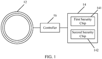
- FIG. 1 is a schematic diagram showing a wearable device according to the present disclosure.
- the wearable device of the present disclosure includes an antenna 12, a set of security chips 14 including a first security chip 141 and a second security chip 142, and a controller 16.
- the antenna 12 may be disposed on an external face of an outer case of the wearable device.
- the set of security chips 14 and the controller 16 are disposed inside the outer case of the wearable device.
- the set of security chips 14 is coupled to the antenna 12.
- the controller 16 is disposed between the set of security chips 14 and the antenna 12.
- the controller 16 is coupled between the set of security chips 14 and the antenna 12.
- the antenna 12 is configured to transmit and receive an electromagnetic signal (i.e., a short distance communication signal). Specifically, when one security chip in the set of security chips 14 is to transmit a signal to an external device (e.g., a card reader), the antenna 12 is applied with an electric current varying with time to generate the electromagnetic signal. Alternatively, when the external device is to transmit a signal to one security chip in the set of security chips 14, the antenna 12 generates an electric current varying with time due to the external electromagnetic signal such that the one security chip can receive a signal transmitted from the external device. That is to say, the antenna 12 is used to deliver the electromagnetic signal to enable communication between the wearable device and the external device.
- an electromagnetic signal i.e., a short distance communication signal
- the security chips in the set of security chips 14 are used to process private information of a user. Specifically, both of the first security chip 141 and the second security chip 142 are used to process the private information of the user.
- the first security chip 141 and the security chip 142 are security chips of different types of electronic cards, for example, the transportation card and the entrance card.
- the first security chip 141 and the second security chip 142 belong to a same type of electronic card but they are security chips of two card entities, for example, two pieces of stored-value cards.
- the controller 16 is configured to enable one of the first security chip 141 and the second security chip 142 based on a user operation, to transmit and receive the electromagnetic signal or the short distance communication signal via the antenna 12. Specifically, the controller 16 enables one security chip in the set of security chips 14 and disables all the other security chips in the set of security chips 14. In an example, assuming that the set of security chips 14 includes the first security chip 141, the second security chip 142, and a third security chip (not shown), the controller 16 may enable the first security chip 141 and disable all the other security chips including the second security chip 142 and the third security chip.
- the user when the user wants to use one electronic card (corresponding to one security chip) deployed in the wearable device, the user may have the controller 16 selecting the one security chip via the user operation to transmit and receive the short distance communication via the antenna 12 and have all the other security chips in a disabled state. In such a way, the user uses only one electronic card at a time. This avoids signal interference or other security issues.
- the controller 16 is configured to enable one of the first security chip 141 and the second security chip 142 for a predetermined period of time.
- one electronic card is activated by the user, and the one electronic card will be automatically deactivated after the predetermined period of time (e.g., 10 seconds). This can increase security, avoid skimming or eavesdropping, and reduce power consumption.
- the controller 16 may establish a path of connection between the antenna 12 and one the security chip and disconnect paths of connection between the antenna 12 and all the other security chips to enable the one security chip and disable all the other security chips. For example, the controller 16 establishes a path of connection between the first security chip 141 and the antenna 12 and disconnects a path of connection between the second security chip 142 and the antenna 12. In another aspect, the controller 16 may connect a security chip to a power source to enable the security chip and disconnect a security chip from the power source to disable the security chip.
- two or more than two short distance communication chips e.g., conforming with RFID or NFC communication standard
- the user can select one of the communication chips to carry out the short distance communication with the external device. This improves convenience for the user in using the electronic cards.
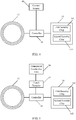
- FIG. 2 is a schematic diagram showing a wearable device according to a first embodiment of the present disclosure.
- the wearable device further includes a button or knob 20 coupled to the controller 16.
- the button or knob 20 is disposed on an external face of the wearable device.
- the controller 16 receives the user operation via the button or knob 20 to enable one of the security chips. That is to say, the user selects one of the security chips via the button or knob 20 to execute the short distance communication.
- FIG. 3 is a schematic diagram showing a wearable device according to a second embodiment of the present disclosure.
- the wearable device further includes a touch panel 30 coupled to the controller 16.
- the controller 16 receives the user operation via the touch panel 30 to enable one of the security chips. That is to say, touch operations made by the user on the touch panel 30 can select one of the security chips to execute the short distance communication.
- the touch panel 30 may combine with a display panel (not shown) to form a touch screen.
- the wearable device can be a smartwatch having the touch screen.
- FIG. 4 is a schematic diagram showing a wearable device according to a third embodiment of the present disclosure.
- the wearable device further includes a gesture sensor 40 coupled to the controller 16.
- the gesture sensor 40 may be disposed inside the outer case of the wearable device.
- the gesture sensor 40 is configured to sense a gesture, a posture, or a motion of the user to generate a sensing signal.
- the controller 16 receives the sensing signal and enables one of the security chips based on the sensing signal. That is to say, when the user wears the wearable device, a gesture identifiable by the gesture sensor 40 may be made by the user to enable one of the security chips. For example, one times of a rotational motion can enable the first security chip 141 and disable the second security chip 142, and two times of the rotational motion can disable the first security chip 141 and enable the second security chip 142.
- FIG. 5 is a schematic diagram showing a wearable device according to a fourth embodiment of the present disclosure.
- the wearable device further includes a transparent conductive film 50 and a touch detector 52.
- the transparent conductive film 50 is electrically connected to the touch detector 52.
- the touch detector 52 is coupled to the controller 16.
- the transparent conductive film 50 is disposed on the external face of the wearable device.
- the touch detector 52 is disposed inside the outer case of the wearable device.
- the transparent conductive film 50 and the touch detector 52 serve as an input device configured to receive a user input to achieve security chip switch function.
- FIG. 6 is a schematic diagram showing a transparent conductive film according to the present disclosure.
- the transparent conductive film 50 is a conductive film formed in a mesh shape.
- the mesh shape is formed by a plurality of ultra-fine metal lines.
- the transparent conductive film 50 is divided into a plurality of regions. These regions are electrically disconnected from each other.
- FIG. 6 is illustrated with two regions (i.e., a first region 511 and a second region 512). It can be understood that the transparent conductive film 50 can be divided into more than two regions that are electrically disconnected from each other.
- Each region includes a plurality of conductive wires 501 that are interlaced with each other to construct a plurality of conductive units 502.
- An integral effect of electrical signal changes (e.g., voltage or current signal changes) of all of the conductive units 502 in each region is generated by an approximal action or a touch action performed above or onto the region. For example, when a user's finger touches a region, a change of electric charges is generated in the region. By detecting electric charge changes of each region, it can be known which region is touched by the user's finger.
- the touch detector 52 is electrically connected to the regions of the transparent conductive film 50. Specifically, each region of the transparent conductive film 50 is connected to the touch detector 52 via a transmission wire. The touch detector 52 can detect changes of electric charges on the regions to determine which region is touched.
- the touch detector 52 detects an integral effect of electrical signal changes of all of the conductive units 502 in each region to output a detecting signal.
- the controller 16 receives the detecting signal transmitted from the touch detector 52 to enable one security chip and disable all the other security chips.
- the first security chip 141 corresponds to the first region 511 and the second security chip 142 corresponds to the second region 512.
- the first security chip 141 is enabled when the user clicks the first region 511
- the second security chip 142 is enabled when the user clicks the second region 512.
- the first security chip 141 is enabled and the second security chip 142 is disabled when the user's finger slides from the first region 511 to the second region 512
- the second security chip 142 is enabled and the first security chip 141 is disabled when the user's finger slides from the second region 512 to the first region 511.
- FIG. 7 is a schematic diagram showing a wristwatch according to the present disclosure.
- the wearable device of the present disclosure can be a wristwatch.
- the wristwatch includes a housing, which includes a transparent cover 71 and an external cover 72.
- the transparent cover 71 is made of a transparent material (e.g., glass). A part of the housing if formed by the transparent cover 71.
- a receiving room is defined by the transparent cover 71 and the external cover 72.
- the wristwatch further includes a dial 73, a plurality of physical scales 74, and a plurality of physical indicators 75 that are disposed in the receiving room.
- the physical scales (e.g., hour scales) 74 are formed on a face of the dial 73.
- the physical indicators e.g., a hour hand, minute hand, and second hand
- the physical indicators 75 cooperate with the physical scales 74 to show the time. Through the transparent cover 71, the user can perceive the position information (i.e., the time information) indicated by the physical indicators 75.
- the transparent conductive film 50 is attached to a face (e.g., an inner face) of the transparent cover 71, the antenna 12 is disposed at any appropriate location of the wristwatch where signals are not significantly interfered, and the receiving room of the wristwatch receives the touch detector 52, the controller 16, and the set of security chips 14 having two or more than two security chips. In this way, switch function of the short distance communication chips can be achieved in a traditional wristwatch.
- FIG. 8 is a flowchart of a short distance communication switch method according to the present disclosure. Referring to FIG. 8 with reference to the above context, the method includes the following steps.
- Step S82 the antenna 12 is provided for transmitting and receiving an electromagnetic signal to achieve short distance communication.
- the antenna 12 is disposed in the wearable device for transmit and receive a short distance communication signal conforming with RFID or NFC standard.
- Step S84 one security chip in the set of security chips 14 disposed in the wearable device is enabled to transmit and receive the electromagnetic signal via the antenna 12, and all the other security chips in the set of security chips 14 are disabled.
- the set of security chips 14 coupled to the antenna 12 and the controller 16 disposed between the antenna 12 and the set of security chips 14 are deployed in the wearable device.
- the set of security chips 14 includes two or more than two security chips (e.g., the first security chip 141 and the second security chip 142).
- the controller 16 enables one security chip in the set of security chips 14 and disables all the other security chips in the set of security chips 14.
- the enabled security chip can transmit and receive the short distance communication signal via the antenna 12.
Landscapes
- Engineering & Computer Science (AREA)
- Theoretical Computer Science (AREA)
- Physics & Mathematics (AREA)
- General Physics & Mathematics (AREA)
- Computer Networks & Wireless Communication (AREA)
- Computer Hardware Design (AREA)
- General Engineering & Computer Science (AREA)
- Business, Economics & Management (AREA)
- Computer Security & Cryptography (AREA)
- Signal Processing (AREA)
- Human Computer Interaction (AREA)
- General Business, Economics & Management (AREA)
- Strategic Management (AREA)
- Accounting & Taxation (AREA)
- Software Systems (AREA)
- Microelectronics & Electronic Packaging (AREA)
- Mathematical Physics (AREA)
- Electric Clocks (AREA)
- Lock And Its Accessories (AREA)
- User Interface Of Digital Computer (AREA)
Abstract
A wearable device includes an antenna (12) configured to transmit and receive a short distance communication signal; a set of security chips (14) coupled to the antenna (12), including a plurality of security chips (141, 142) configured to process private information of a user; and a controller (16) disposed between the antenna (12) and the set of security chips (14), configured to enable one of the security chips (141, 142) in the set of security chips (14) based on a user operation, to transmit and receive the short distance communication signal via the antenna (12). A wristwatch and a short distance communication switch method are also provided. The user can select one of communication chips to carry out short distance communication with an external device. This improves convenience in using the electronic cards.
Description
- The present disclosure relates to short distance communication technologies, and more particularly, to a wearable device, wristwatch, and a short distance communication switch method.
- Short distance communication has been widely used in various application scenarios. Radio frequency identification (RFID) and near field communication (NFC) are common short distance communication technologies. Also, physical or virtual electronic cards, such as a transportation card, an entrance card, and an electronic payment card, conforming with RFID or NFC communication standard are widely used in a human's daily life.
- Users of the electronic cards often have to carry various types of the physical cards. Even though current technologies can virtualize the cards and integrate them to smartphones, there are many physical electronic cards that still cannot be virtualized or are not in support of Virtualization. This makes the users inevitably have to carry these physical cards, and thus increases inconvenience. Accordingly, there is a need to provide a new solution to solve this problem.
- The present disclosure provides a wearable device, a wristwatch, and a short distance communication switch method, for increasing convenience for a user in using electronic cards.
- An aspect of the present disclosure provides a wearable device, including an antenna configured to transmit and receive a short distance communication signal; a set of security chips coupled to the antenna, including a plurality of security chips configured to process private information of a user; and a controller disposed between the antenna and the set of security chips , configured to enable one of the security chips in the set of security chips based on a user operation, to transmit and receive the short distance communication signal via the antenna.
- Another aspect of the present disclosure provides a wristwatch, including a housing forming a receiving room, a part of the housing formed by a transparent cover, the wristwatch further including a dial, physical scales on a face of the dial, and physical indicators disposed above the dial and cooperating with the physical scales to show the time, the wristwatch further including an antenna configured to transmit and receive a short distance communication signal; a set of security chips coupled to the antenna, including a plurality of security chips configured to process private information of a user; a transparent conductive film attached to a face of the transparent cover, the transparent conductive film divided into a plurality of regions, each of the regions including a plurality of conductive wires that are interlaced with each other to construct a plurality of conductive units; a touch detector disposed in the receiving room and electrically connecting to the regions of the transparent conductive film, configured to detect an integral effect of electrical signal changes of all of the conductive units in each region to output a detecting signal; and a controller disposed in the receiving room, coupled to the touch detector, the set of security chips, and the antenna, configured to receive the detecting signal transmitted from the touch detector to enable one of the security chips in the set of security chips, to transmit and receive the short distance communication signal via the antenna.
- Still another aspect of the present disclosure provides a short distance communication switch method, including providing an antenna for transmitting and receiving an electromagnetic signal to achieve short distance communication; and enabling one of security chips in a set of security chips disposed in a wearable device to transmit and receive the electromagnetic signal via the antenna, and disabling all the others of the security chips in the set of security chips.
- In the wearable device of the present disclosure, two or more than two short distance communication chips (e.g., conforming with RFID or NFC communication standard) are deployed. The user can select one of the communication chips to carry out the short distance communication with the external device. This improves convenience for the user in using the electronic cards.
-
-
FIG. 1 is a schematic diagram showing a wearable device according to the present disclosure. -
FIG. 2 is a schematic diagram showing a wearable device according to a first embodiment of the present disclosure. -
FIG. 3 is a schematic diagram showing a wearable device according to a second embodiment of the present disclosure. -
FIG. 4 is a schematic diagram showing a wearable device according to a third embodiment of the present disclosure. -
FIG. 5 is a schematic diagram showing a wearable device according to a fourth embodiment of the present disclosure. -
FIG. 6 is a schematic diagram showing a transparent conductive film according to the present disclosure. -
FIG. 7 is a schematic diagram showing a wristwatch according to the present disclosure. -
FIG. 8 is a flowchart of a short distance communication switch method according to the present disclosure. - To make the objectives, technical schemes, and technical effects of the present disclosure more clearly and definitely, the present disclosure will be described in details below by using embodiments in conjunction with the appending drawings. It should be understood that the specific embodiments described herein are merely for explaining the present disclosure, and as used herein, the term "embodiment" refers to an instance, an example, or an illustration but is not intended to limit the present disclosure. In addition, the articles "a" and "an" as used in the specification and the appended claims should generally be construed to mean "one or more" unless specified otherwise or clear from the context to be directed to a singular form.
- The present disclosure provides a wearable device including a plurality of security chips configured for short distance communication. The short distance communication includes radio frequency identification (RFID) communication and near field communication (NFC), but is not limited thereto. A user may switch to one of the security chips and use it based on different situation demands. For example, one of electronic cards is used for the short distance communication. Accordingly, user convenience is improved.
- In an example, a transportation card and an entrance card equipped with short distance communication function are deployed in the wearable device. The user may use a security chip of the transportation card for authentication when commuting and use the entrance card when reaching home. A card having electronic payment function may be incorporated in the wearable device. The types of the electronic cards are not limited in the present disclosure as long as they are equipped with the short distance communication function.
- The following examples are illustrated with a wearable device having two security chips. It can be understood that the wearable device may have two or more than two security chips.
-
FIG. 1 is a schematic diagram showing a wearable device according to the present disclosure. The wearable device of the present disclosure includes anantenna 12, a set ofsecurity chips 14 including afirst security chip 141 and asecond security chip 142, and acontroller 16. Theantenna 12 may be disposed on an external face of an outer case of the wearable device. The set ofsecurity chips 14 and thecontroller 16 are disposed inside the outer case of the wearable device. The set ofsecurity chips 14 is coupled to theantenna 12. Thecontroller 16 is disposed between the set ofsecurity chips 14 and theantenna 12. Preferably, thecontroller 16 is coupled between the set ofsecurity chips 14 and theantenna 12. - The
antenna 12 is configured to transmit and receive an electromagnetic signal (i.e., a short distance communication signal). Specifically, when one security chip in the set ofsecurity chips 14 is to transmit a signal to an external device (e.g., a card reader), theantenna 12 is applied with an electric current varying with time to generate the electromagnetic signal. Alternatively, when the external device is to transmit a signal to one security chip in the set ofsecurity chips 14, theantenna 12 generates an electric current varying with time due to the external electromagnetic signal such that the one security chip can receive a signal transmitted from the external device. That is to say, theantenna 12 is used to deliver the electromagnetic signal to enable communication between the wearable device and the external device. - The security chips in the set of
security chips 14 are used to process private information of a user. Specifically, both of thefirst security chip 141 and thesecond security chip 142 are used to process the private information of the user. In an embodiment, thefirst security chip 141 and thesecurity chip 142 are security chips of different types of electronic cards, for example, the transportation card and the entrance card. In an embodiment, thefirst security chip 141 and thesecond security chip 142 belong to a same type of electronic card but they are security chips of two card entities, for example, two pieces of stored-value cards. - The
controller 16 is configured to enable one of thefirst security chip 141 and thesecond security chip 142 based on a user operation, to transmit and receive the electromagnetic signal or the short distance communication signal via theantenna 12. Specifically, thecontroller 16 enables one security chip in the set ofsecurity chips 14 and disables all the other security chips in the set ofsecurity chips 14. In an example, assuming that the set ofsecurity chips 14 includes thefirst security chip 141, thesecond security chip 142, and a third security chip (not shown), thecontroller 16 may enable thefirst security chip 141 and disable all the other security chips including thesecond security chip 142 and the third security chip. - That is to say, when the user wants to use one electronic card (corresponding to one security chip) deployed in the wearable device, the user may have the
controller 16 selecting the one security chip via the user operation to transmit and receive the short distance communication via theantenna 12 and have all the other security chips in a disabled state. In such a way, the user uses only one electronic card at a time. This avoids signal interference or other security issues. - Further, the
controller 16 is configured to enable one of thefirst security chip 141 and thesecond security chip 142 for a predetermined period of time. In an example, one electronic card is activated by the user, and the one electronic card will be automatically deactivated after the predetermined period of time (e.g., 10 seconds). This can increase security, avoid skimming or eavesdropping, and reduce power consumption. - Specifically, the
controller 16 may establish a path of connection between theantenna 12 and one the security chip and disconnect paths of connection between theantenna 12 and all the other security chips to enable the one security chip and disable all the other security chips. For example, thecontroller 16 establishes a path of connection between thefirst security chip 141 and theantenna 12 and disconnects a path of connection between thesecond security chip 142 and theantenna 12. In another aspect, thecontroller 16 may connect a security chip to a power source to enable the security chip and disconnect a security chip from the power source to disable the security chip. - In the wearable device of the present disclosure, two or more than two short distance communication chips (e.g., conforming with RFID or NFC communication standard) are deployed. The user can select one of the communication chips to carry out the short distance communication with the external device. This improves convenience for the user in using the electronic cards.
-
FIG. 2 is a schematic diagram showing a wearable device according to a first embodiment of the present disclosure. In the first embodiment, the wearable device further includes a button orknob 20 coupled to thecontroller 16. The button orknob 20 is disposed on an external face of the wearable device. Thecontroller 16 receives the user operation via the button orknob 20 to enable one of the security chips. That is to say, the user selects one of the security chips via the button orknob 20 to execute the short distance communication. -
FIG. 3 is a schematic diagram showing a wearable device according to a second embodiment of the present disclosure. In the second embodiment, the wearable device further includes atouch panel 30 coupled to thecontroller 16. Thecontroller 16 receives the user operation via thetouch panel 30 to enable one of the security chips. That is to say, touch operations made by the user on thetouch panel 30 can select one of the security chips to execute the short distance communication. Thetouch panel 30 may combine with a display panel (not shown) to form a touch screen. The wearable device can be a smartwatch having the touch screen. -
FIG. 4 is a schematic diagram showing a wearable device according to a third embodiment of the present disclosure. In the third embodiment, the wearable device further includes agesture sensor 40 coupled to thecontroller 16. Thegesture sensor 40 may be disposed inside the outer case of the wearable device. Thegesture sensor 40 is configured to sense a gesture, a posture, or a motion of the user to generate a sensing signal. Thecontroller 16 receives the sensing signal and enables one of the security chips based on the sensing signal. That is to say, when the user wears the wearable device, a gesture identifiable by thegesture sensor 40 may be made by the user to enable one of the security chips. For example, one times of a rotational motion can enable thefirst security chip 141 and disable thesecond security chip 142, and two times of the rotational motion can disable thefirst security chip 141 and enable thesecond security chip 142. -
FIG. 5 is a schematic diagram showing a wearable device according to a fourth embodiment of the present disclosure. In the fourth embodiment, the wearable device further includes a transparentconductive film 50 and atouch detector 52. The transparentconductive film 50 is electrically connected to thetouch detector 52. Thetouch detector 52 is coupled to thecontroller 16. The transparentconductive film 50 is disposed on the external face of the wearable device. Thetouch detector 52 is disposed inside the outer case of the wearable device. The transparentconductive film 50 and thetouch detector 52 serve as an input device configured to receive a user input to achieve security chip switch function. -
FIG. 6 is a schematic diagram showing a transparent conductive film according to the present disclosure. As shown inFIG. 6 , the transparentconductive film 50 is a conductive film formed in a mesh shape. In practice, the mesh shape is formed by a plurality of ultra-fine metal lines. The transparentconductive film 50 is divided into a plurality of regions. These regions are electrically disconnected from each other.FIG. 6 is illustrated with two regions (i.e., afirst region 511 and a second region 512). It can be understood that the transparentconductive film 50 can be divided into more than two regions that are electrically disconnected from each other. Each region includes a plurality ofconductive wires 501 that are interlaced with each other to construct a plurality ofconductive units 502. An integral effect of electrical signal changes (e.g., voltage or current signal changes) of all of theconductive units 502 in each region is generated by an approximal action or a touch action performed above or onto the region. For example, when a user's finger touches a region, a change of electric charges is generated in the region. By detecting electric charge changes of each region, it can be known which region is touched by the user's finger. Thetouch detector 52 is electrically connected to the regions of the transparentconductive film 50. Specifically, each region of the transparentconductive film 50 is connected to thetouch detector 52 via a transmission wire. Thetouch detector 52 can detect changes of electric charges on the regions to determine which region is touched. Thetouch detector 52 detects an integral effect of electrical signal changes of all of theconductive units 502 in each region to output a detecting signal. Thecontroller 16 receives the detecting signal transmitted from thetouch detector 52 to enable one security chip and disable all the other security chips. - For example, the
first security chip 141 corresponds to thefirst region 511 and thesecond security chip 142 corresponds to thesecond region 512. In an example, thefirst security chip 141 is enabled when the user clicks thefirst region 511, thesecond security chip 142 is enabled when the user clicks thesecond region 512. In another example, thefirst security chip 141 is enabled and thesecond security chip 142 is disabled when the user's finger slides from thefirst region 511 to thesecond region 512, thesecond security chip 142 is enabled and thefirst security chip 141 is disabled when the user's finger slides from thesecond region 512 to thefirst region 511. - It can be understood by a person skilled in the art that using the transparent
conductive film 50 to detect user operations as described above is apparently different from touch operation sensing technologies used in conventional touch panels and image display technologies with pixel electrodes used in conventional display panels. -
FIG. 7 is a schematic diagram showing a wristwatch according to the present disclosure. The wearable device of the present disclosure can be a wristwatch. As shown inFIG. 7 , the wristwatch includes a housing, which includes atransparent cover 71 and anexternal cover 72. Thetransparent cover 71 is made of a transparent material (e.g., glass). A part of the housing if formed by thetransparent cover 71. A receiving room is defined by thetransparent cover 71 and theexternal cover 72. The wristwatch further includes adial 73, a plurality ofphysical scales 74, and a plurality ofphysical indicators 75 that are disposed in the receiving room. The physical scales (e.g., hour scales) 74 are formed on a face of thedial 73. The physical indicators (e.g., a hour hand, minute hand, and second hand) 75 are disposed above thedial 73. Thephysical indicators 75 cooperate with thephysical scales 74 to show the time. Through thetransparent cover 71, the user can perceive the position information (i.e., the time information) indicated by thephysical indicators 75. - In an embodiment, the transparent
conductive film 50 is attached to a face (e.g., an inner face) of thetransparent cover 71, theantenna 12 is disposed at any appropriate location of the wristwatch where signals are not significantly interfered, and the receiving room of the wristwatch receives thetouch detector 52, thecontroller 16, and the set ofsecurity chips 14 having two or more than two security chips. In this way, switch function of the short distance communication chips can be achieved in a traditional wristwatch. -
FIG. 8 is a flowchart of a short distance communication switch method according to the present disclosure. Referring toFIG. 8 with reference to the above context, the method includes the following steps. - In Step S82, the
antenna 12 is provided for transmitting and receiving an electromagnetic signal to achieve short distance communication. - As shown in
FIG. 1 , theantenna 12 is disposed in the wearable device for transmit and receive a short distance communication signal conforming with RFID or NFC standard. - In Step S84, one security chip in the set of
security chips 14 disposed in the wearable device is enabled to transmit and receive the electromagnetic signal via theantenna 12, and all the other security chips in the set ofsecurity chips 14 are disabled. - As shown in
FIG. 1 , the set ofsecurity chips 14 coupled to theantenna 12 and thecontroller 16 disposed between theantenna 12 and the set ofsecurity chips 14 are deployed in the wearable device. The set ofsecurity chips 14 includes two or more than two security chips (e.g., thefirst security chip 141 and the second security chip 142). Thecontroller 16 enables one security chip in the set ofsecurity chips 14 and disables all the other security chips in the set ofsecurity chips 14. The enabled security chip can transmit and receive the short distance communication signal via theantenna 12. - Other details of the short distance communication switch method of the present disclosure can be referred to the descriptions on the wearable device and the wristwatch in the above context, and are not repeated herein.
- While the preferred embodiments of the present disclosure have been illustrated and described in detail, various modifications and alterations can be made by persons skilled in this art. The embodiment of the present disclosure is therefore described in an illustrative but not restrictive sense. It is intended that the present disclosure should not be limited to the particular forms as illustrated, and that all modifications and alterations which maintain the realm of the present disclosure are within the scope as defined in the appended claims.
Claims (15)
- A wearable device, characterized in that the wearable device comprises:an antenna (12) configured to transmit and receive a short distance communication signal;a set of security chips (14) coupled to the antenna (12), comprising a plurality of security chips (141, 142) configured to process private information of a user; anda controller (16) disposed between the antenna (12) and the set of security chips (14), configured to enable one of the security chips (141, 142) in the set of security chips (14) based on a user operation, to transmit and receive the short distance communication signal via the antenna (12).
- The wearable device according to claim 1, characterized in that the controller (16) is configured to enable one of the security chips (141, 142) and disable all the others of the security chips (141, 142).
- The wearable device according to claim 2, characterized in that the controller (16) is configured to establish a path of connection between the antenna (12) and one of the security chips (141, 142) and disconnect paths of connection between the antenna (12) and all the others of the security chips (141, 142) to enable the one of the security chips (141, 142) and disable all the others of the security chips (141, 142).
- The wearable device according to claim 1, characterized in that the controller (16) is configured to enable one of the security chips (141, 142) for a predetermined period of time.
- The wearable device according to claim 1, characterized in that the set of security chips (14) comprises two or more than two security chips (141, 142).
- The wearable device according to claim 1, characterized in that the short distance communication signal conforms with radio frequency identification (RFID) and/or near field communication (NFC) standards.
- The wearable device according to claim 1, characterized in that the wearable device further comprises a button or knob (20) coupled to the controller (16), wherein the controller (16) receives the user operation via the button or knob (20) to enable one of the security chips (141, 142).
- The wearable device according to claim 1, characterized in that the wearable device further comprises a touch panel (30) coupled to the controller (16), wherein the controller (16) receives the user operation via the touch panel (30) to enable one of the security chips (141, 142).
- The wearable device according to claim 1, characterized in that the wearable device further comprises a gesture sensor (40) coupled to the controller (16) and configured to sense a hand gesture of a user to generate a sensing signal, wherein the controller (16) receives the sensing signal and enables one of the security chips (141, 142) based on the sensing signal.
- The wearable device according to claim 1, characterized in that the wearable device further comprises:a transparent conductive film (50) divided into a plurality of regions (511, 512), each of the regions (511, 512) comprising a plurality of conductive wires (501) that are interlaced with each other to construct a plurality of conductive units (502); anda touch detector (52) coupled to the controller (16) and electrically connected to the regions (511, 512) of the transparent conductive film (50), configured to detect an integral effect of electrical signal changes of all of the conductive units (502) in each region (511, 512) to output a detecting signal,wherein the controller (16) receives the detecting signal transmitted from the touch detector (52) to enable one of the security chips (141, 142).
- The wearable device according to claim 1, characterized in that the wearable device further comprises the wearable device is a wristwatch comprising a housing forming a receiving room, a part of the housing is formed by a transparent cover (71), the wristwatch further comprises a dial (73), physical scales (74) on a face of the dial (73), and physical indicators (75) disposed above the dial (73), and the physical indicators (75) cooperate with the physical scales (74) to show the time.
- A wristwatch, comprising a housing forming a receiving room, a part of the housing formed by a transparent cover (71), the wristwatch further comprising a dial (73), physical scales (74) on a face of the dial (73), and physical indicators (75) disposed above the dial (73) and cooperating with the physical scales (74) to show the time, characterized in that the wearable device further comprises:an antenna (12) configured to transmit and receive a short distance communication signal;a set of security chips (14) coupled to the antenna (12), comprising a plurality of security chips (141, 142) configured to process private information of a user;a transparent conductive film (50) attached to a face of the transparent cover (71), the transparent conductive film (50) divided into a plurality of regions (511, 512), each of the regions (511, 512) comprising a plurality of conductive wires (501) that are interlaced with each other to construct a plurality of conductive units (502);a touch detector (52) disposed in the receiving room and electrically connecting to the regions (511, 512) of the transparent conductive film (50), configured to detect an integral effect of electrical signal changes of all of the conductive units (502) in each region (511, 512) to output a detecting signal; anda controller (16) disposed in the receiving room, coupled to the touch detector (52), the set of security chips (14), and the antenna (12), configured to receive the detecting signal transmitted from the touch detector (52) to enable one of the security chips (141, 142) in the set of security chips (14), to transmit and receive the short distance communication signal via the antenna (12).
- The wristwatch according to claim 12, characterized in that the controller (16) is configured to enable one of the security chips (141, 142) and disable all the others of the security chips (141, 142).
- The wristwatch according to claim 12, characterized in that the controller (16) is configured to enable one of the security chips (141, 142) for a predetermined period of time.
- A short distance communication switch method, characterized in that the method comprises:providing an antenna (12) for transmitting and receiving an electromagnetic signal to achieve short distance communication; andenabling one of security chips (141, 142) in a set of security chips (14) disposed in a wearable device to transmit and receive the electromagnetic signal via the antenna (12), and disabling all the others of the security chips (141, 142) in the set of security chips (14).
Applications Claiming Priority (1)
| Application Number | Priority Date | Filing Date | Title |
|---|---|---|---|
| TW107109507A TWI679856B (en) | 2018-03-20 | 2018-03-20 | Wearable device, wristwatch, and short distance communication switch method |
Publications (1)
| Publication Number | Publication Date |
|---|---|
| EP3543935A1 true EP3543935A1 (en) | 2019-09-25 |
Family
ID=62909330
Family Applications (1)
| Application Number | Title | Priority Date | Filing Date |
|---|---|---|---|
| EP18179690.5A Withdrawn EP3543935A1 (en) | 2018-03-20 | 2018-06-25 | Wearable device, wristwatch, and short distance communication switch method |
Country Status (6)
| Country | Link |
|---|---|
| US (1) | US20190294209A1 (en) |
| EP (1) | EP3543935A1 (en) |
| JP (1) | JP2019164741A (en) |
| KR (1) | KR102196964B1 (en) |
| CN (1) | CN110308766A (en) |
| TW (1) | TWI679856B (en) |
Families Citing this family (2)
| Publication number | Priority date | Publication date | Assignee | Title |
|---|---|---|---|---|
| CN111657929B (en) * | 2020-07-21 | 2023-08-25 | 广东高驰运动科技股份有限公司 | Wearable device and method of use |
| CN117751365A (en) * | 2022-07-20 | 2024-03-22 | 京东方科技集团股份有限公司 | Driving circuit, display device and driving method |
Citations (3)
| Publication number | Priority date | Publication date | Assignee | Title |
|---|---|---|---|---|
| CN104766105A (en) * | 2014-01-06 | 2015-07-08 | 和硕联合科技股份有限公司 | Wearable device and operation method thereof |
| KR20170026007A (en) * | 2015-08-31 | 2017-03-08 | 엘지전자 주식회사 | Hybrid smart watch and operating method thereof |
| US20170199497A1 (en) * | 2016-01-12 | 2017-07-13 | Princo Corp. | Smart wristwatch structure |
Family Cites Families (14)
| Publication number | Priority date | Publication date | Assignee | Title |
|---|---|---|---|---|
| US4255802A (en) * | 1977-11-29 | 1981-03-10 | Citizen Watch Company Limited | Electronic timepiece |
| JPH0855200A (en) * | 1994-08-11 | 1996-02-27 | N T T Data Tsushin Kk | Ic card |
| KR100834845B1 (en) * | 2007-04-13 | 2008-06-03 | 주식회사 하렉스인포텍 | Contactless card |
| JP2011070321A (en) * | 2009-09-24 | 2011-04-07 | Maxell Seiki Kk | Multi-application ic card, and ic card |
| CN103197529A (en) * | 2013-02-06 | 2013-07-10 | 方科峰 | Motion sensing wrist watch and application method thereof |
| US9001082B1 (en) * | 2013-09-27 | 2015-04-07 | Sensel, Inc. | Touch sensor detector system and method |
| KR102177802B1 (en) * | 2014-05-28 | 2020-11-11 | 삼성전자주식회사 | Apparatas and method for including a multi subscriber identity module in an electronic device |
| KR102287160B1 (en) * | 2014-07-31 | 2021-08-06 | 엘지전자 주식회사 | The wearble device and control method thereof |
| CN104091188B (en) * | 2014-07-31 | 2017-06-20 | 百度在线网络技术(北京)有限公司 | Wearable and smart card system |
| US20160156603A1 (en) * | 2014-11-28 | 2016-06-02 | Craig Janik | Low Power Secure User Identity Authentication Ring |
| US10372274B2 (en) * | 2015-04-13 | 2019-08-06 | Semiconductor Energy Laboratory Co., Ltd. | Semiconductor device and touch panel |
| KR102497528B1 (en) * | 2016-01-21 | 2023-02-08 | 엘지전자 주식회사 | Watch type terminal |
| CN205656623U (en) * | 2016-04-29 | 2016-10-19 | 华美电子股份有限公司 | Wearing formula device and certification system with authentication function |
| US10270763B2 (en) * | 2016-09-14 | 2019-04-23 | David LIPOVKOV | Virtual SIM authentication |
-
2018
- 2018-03-20 TW TW107109507A patent/TWI679856B/en active
- 2018-06-04 CN CN201810561345.2A patent/CN110308766A/en active Pending
- 2018-06-06 US US16/001,353 patent/US20190294209A1/en not_active Abandoned
- 2018-06-25 EP EP18179690.5A patent/EP3543935A1/en not_active Withdrawn
- 2018-07-17 JP JP2018133882A patent/JP2019164741A/en active Pending
- 2018-12-10 KR KR1020180158482A patent/KR102196964B1/en active IP Right Grant
Patent Citations (3)
| Publication number | Priority date | Publication date | Assignee | Title |
|---|---|---|---|---|
| CN104766105A (en) * | 2014-01-06 | 2015-07-08 | 和硕联合科技股份有限公司 | Wearable device and operation method thereof |
| KR20170026007A (en) * | 2015-08-31 | 2017-03-08 | 엘지전자 주식회사 | Hybrid smart watch and operating method thereof |
| US20170199497A1 (en) * | 2016-01-12 | 2017-07-13 | Princo Corp. | Smart wristwatch structure |
Also Published As
| Publication number | Publication date |
|---|---|
| US20190294209A1 (en) | 2019-09-26 |
| JP2019164741A (en) | 2019-09-26 |
| TW201941549A (en) | 2019-10-16 |
| CN110308766A (en) | 2019-10-08 |
| TWI679856B (en) | 2019-12-11 |
| KR102196964B1 (en) | 2020-12-31 |
| KR20200068531A (en) | 2020-06-15 |
Similar Documents
| Publication | Publication Date | Title |
|---|---|---|
| CN108736586B (en) | Electronic device comprising a plurality of coils | |
| US10056933B2 (en) | Electronic device and method for controlling display on basis of information of accessory device and accessory device related thereto | |
| EP3367644B1 (en) | Electronic device including bent display and method of displaying image on bent display | |
| EP3375041B1 (en) | Antenna device and electronic device including the same | |
| KR102408870B1 (en) | Antenna and electronic device having it | |
| EP3336617A1 (en) | Cradle for wireless charging and electronic device applied to same | |
| KR102396339B1 (en) | Antenna and electronic device having it | |
| KR20160026467A (en) | Electronic device, controlling method thereof and recording medium | |
| KR20160080473A (en) | Watch type mobile terminal and method of controlling the same | |
| KR20150085650A (en) | Method and apparatus for processing input using touch screen | |
| KR102447383B1 (en) | Antenna and electronic device having it | |
| KR102144588B1 (en) | Sensor module and device therewith | |
| EP3543935A1 (en) | Wearable device, wristwatch, and short distance communication switch method | |
| KR20160100674A (en) | Method for recognizing flip cover of electronic device, electronic device, and flip cover | |
| EP3654113B1 (en) | Wristwatch and method for improving security in electronic payment for wristwatch | |
| US20140170981A1 (en) | Electronic apparatus and data transmission method | |
| EP3313054B1 (en) | System with an electronic device having auxiliary device | |
| US10425241B2 (en) | Electronic device, smart home system using electronic device, and method for controlling smart home system | |
| KR20160056578A (en) | Method for processing input and electronic device for supporting the same | |
| EP3462631B1 (en) | Wristwatch and method applicable to wristwatch for controlling magnitude of short distance communication signals | |
| EP3474089A1 (en) | Wristwatch and method applicable to wristwatch for inputting password | |
| KR102704043B1 (en) | Wireless power transmitter-receiver and method for operating thereof | |
| KR20210037377A (en) | Wireless power transmitter-receiver and method for operating thereof |
Legal Events
| Date | Code | Title | Description |
|---|---|---|---|
| PUAI | Public reference made under article 153(3) epc to a published international application that has entered the european phase |
Free format text: ORIGINAL CODE: 0009012 |
|
| STAA | Information on the status of an ep patent application or granted ep patent |
Free format text: STATUS: THE APPLICATION HAS BEEN PUBLISHED |
|
| AK | Designated contracting states |
Kind code of ref document: A1 Designated state(s): AL AT BE BG CH CY CZ DE DK EE ES FI FR GB GR HR HU IE IS IT LI LT LU LV MC MK MT NL NO PL PT RO RS SE SI SK SM TR |
|
| AX | Request for extension of the european patent |
Extension state: BA ME |
|
| STAA | Information on the status of an ep patent application or granted ep patent |
Free format text: STATUS: THE APPLICATION IS DEEMED TO BE WITHDRAWN |
|
| 18D | Application deemed to be withdrawn |
Effective date: 20200603 |