EP3540890A1 - Monitor device, ground fault protection circuit and techniques - Google Patents
Monitor device, ground fault protection circuit and techniques Download PDFInfo
- Publication number
- EP3540890A1 EP3540890A1 EP19163284.3A EP19163284A EP3540890A1 EP 3540890 A1 EP3540890 A1 EP 3540890A1 EP 19163284 A EP19163284 A EP 19163284A EP 3540890 A1 EP3540890 A1 EP 3540890A1
- Authority
- EP
- European Patent Office
- Prior art keywords
- neutral grounding
- grounding resistor
- capacitor
- injection
- resistor
- Prior art date
- Legal status (The legal status is an assumption and is not a legal conclusion. Google has not performed a legal analysis and makes no representation as to the accuracy of the status listed.)
- Granted
Links
Images




Classifications
-
- H—ELECTRICITY
- H02—GENERATION; CONVERSION OR DISTRIBUTION OF ELECTRIC POWER
- H02H—EMERGENCY PROTECTIVE CIRCUIT ARRANGEMENTS
- H02H9/00—Emergency protective circuit arrangements for limiting excess current or voltage without disconnection
- H02H9/08—Limitation or suppression of earth fault currents, e.g. Petersen coil
-
- G—PHYSICS
- G01—MEASURING; TESTING
- G01R—MEASURING ELECTRIC VARIABLES; MEASURING MAGNETIC VARIABLES
- G01R31/00—Arrangements for testing electric properties; Arrangements for locating electric faults; Arrangements for electrical testing characterised by what is being tested not provided for elsewhere
- G01R31/50—Testing of electric apparatus, lines, cables or components for short-circuits, continuity, leakage current or incorrect line connections
-
- H—ELECTRICITY
- H02—GENERATION; CONVERSION OR DISTRIBUTION OF ELECTRIC POWER
- H02H—EMERGENCY PROTECTIVE CIRCUIT ARRANGEMENTS
- H02H1/00—Details of emergency protective circuit arrangements
- H02H1/0007—Details of emergency protective circuit arrangements concerning the detecting means
- H02H1/003—Fault detection by injection of an auxiliary voltage
Definitions
- the disclosure relates to the field of protection devices, and in particular, to neutral grounding resistors.
- Ground fault resistors may be used in conjunction with resistance grounded power systems.
- a neutral grounding resistor may be deployed under conditions where a ground fault is to be limited to a predetermined current.
- Neutral grounding resistors may also be accompanied by a monitor to monitor when degradation of neutral grounding resistor may take place. In some jurisdictions, monitoring of neutral grounding resistors is required during all operation phases for changes in resistance value.
- a fault protection arrangement may include a neutral grounding resistor, the neutral grounding resistor comprising a ground end and a non-ground end.
- the arrangement may further include a sense circuit, coupled to the non-ground end of the neutral grounding resistor.
- the arrangement may include an injection signal generator, coupled to the non-ground end of the neutral grounding resistor, the injection signal generator arranged to generate a frequency of 240 Hz or greater.
- a neutral grounding resistor monitor assembly may include a sense resistor circuit, having an output, arranged to connect to a non-ground end of a neutral grounding resistor and an injection signal generator, arranged to connect to the non-ground end of the neutral grounding resistor, the injection signal generator arranged to generate an alternating current signal.
- the neutral grounding resistor monitor assembly may further include an injection capacitor, the injection capacitor comprising a first electrode coupled to receive a signal from the injection signal generator, and a second electrode, arranged to connect to the non-ground end of the neutral grounding resistor.
- a fault protection method may include connecting a power system to a fault protection arrangement.
- the fault protection arrangement may include a neutral grounding resistor, the neutral grounding resistor comprising a ground end and a non-ground end; a sense circuit, coupled to the non-ground end of the neutral grounding resistor, the sense circuit comprising a sense resistor, and an injection capacitor.
- the fault protection arrangement may include an injection signal generator, coupled to the non-ground end of the neutral grounding resistor.
- the method may also include probing a resistance of the neutral grounding resistor by sending an injection signal from the sense circuit.
- the terms “on,” “overlying,”, “disposed on” and “over” may be used in the following description and claims. “On” “overlying” ,”disposed on” and “over” may be used to indicate that two or more elements are in direct physical contact with one another. Also, the term “on”, “overlying”, “disposed on,” and “over”, may mean that two or more elements are not in direct contact with one another. For example, “over” may mean that one element is above another element while not contacting one another and may have another element or elements in between the two elements.
- FIG. 1A shows a fault protection arrangement 150 according to various embodiments of the disclosure.
- the fault protection arrangement 150 includes a neutral grounding resistor 158, coupled on a non-ground end to a neutral grounding resistor monitor assembly 152.
- the neutral grounding resistor monitor assembly 152 may include a signal generator 154 and a sense circuit 156, where variants of this arrangement are described in more detail with respect to the figures to follow.
- FIG. 1B shows another fault protection arrangement 160 according to various embodiments of the disclosure.
- the fault protection arrangement 160 includes a neutral grounding resistor 158, coupled on a non-ground end to a neutral grounding resistor monitor assembly 162.
- the neutral grounding resistor monitor assembly 162 may include a signal generator 154 and a sense circuit 156, and a capacitor 164, disposed between the sense circuit and non-grounding end of the neutral grounding resistor 158, where variants of this arrangement are described in more detail with respect to the figures to follow.
- FIG. 1C shows a further fault protection arrangement 170 according to various embodiments of the disclosure.
- the fault protection arrangement 170 includes a neutral grounding resistor 158, coupled on a non-ground end to a neutral grounding resistor monitor assembly 172.
- the neutral grounding resistor monitor assembly 172 may include an injection signal generator 154 and a sense circuit 156, capacitor 164, disposed between the injection signal generator 154 and non-grounding end of the neutral grounding resistor 158, and capacitor 176, disposed between the sense circuit 156 and neutral grounding resistor 158, where variants of this arrangement are described in more detail with respect to the figures to follow.
- FIG. ID shows a fault protection arrangement 100 according to various embodiments of the disclosure.
- the fault protection arrangement 100 involves a neutral grounding resistor 102, electrically coupled to ground and coupled to a power system 130.
- the power system 130 may include various known components including transformers and other equipment.
- the neutral grounding resistor 102 may be designed to provide a target resistance over any suitable range, such as 10 ⁇ to thousands of ⁇ . The embodiments are not limited in this context.
- the neutral grounding resistor 102 is designed to present a fixed electrical resistance, to treat a given fault energy received, for example, over a line between the neutral grounding resistor and power system 130.
- the neutral grounding resistor 102 may be coupled to the neutral of a power system to limit fault current, providing a path for grounding current to a transformer neutral. Excessive changes in the resistance value of the neutral grounding resistor 102 may cause harm to a system being protected.
- the fault protection arrangement 100 provides monitoring and control to determine the state of the neutral grounding resistor 102.
- the fault protection arrangement 100 includes a sense circuit 110 and signal generation circuit 120, acting together as a neutral grounding resistor monitor for the neutral grounding resistor 102.
- the signal generation circuit 120 may include injection signal generator 122, while the sense circuit includes capacitor 112.
- the injection signal generator 122 may operate at the kHz to GHz range in various non-limiting embodiments.
- the injection signal generator 122 may operate below approximately 1 MHz in some embodiments.
- a high frequency signal of any suitable waveform is sent by the injection signal generator 122 to the neutral grounding resistor 102 along an electrical path including the capacitor 112.
- the capacitor 112 may be sized to exhibit an appropriate capacitance and breakdown voltage according to the system to be protected.
- the capacitor 112 may exhibit a capacitance of hundreds of picoFarads, nanoFarads, to hundreds of nanoFarads.
- suitable capacitance for the capacitor 112 at an appropriate probe frequency such as 300 kHz, small changes in impedance of the neutral ground resistor 102 may be ascertained, as detailed in the embodiments to follow.
- the repetition frequency of the injection signal generator 122 may range from 240 Hz to 10 MHz, while the edge rate range from 240 Hz to 10 GHz. In particular embodiments, the repetition rate may range from 100 kHz to 5 MHz, while the edge rate ranged from 100 kHz to 1 GHz.
- the signals generated by injection signal generator 122 may be used to probe resistance of a neutral grounding resistor in open state, short circuit state, or a changing value under normal operation.
- system inductance, NGR inductance, connection inductance, system capacitance, NGR capacitance, and connection capacitance may be probed by the signals.
- the signal generation circuit may further include an alarm circuit 124, to generate an alarm signal when the resistance of the neutral grounding resistor 102 falls outside of a predetermined range.
- FIG. 2A shows a protection arrangement 200 according to additional embodiments of the disclosure.
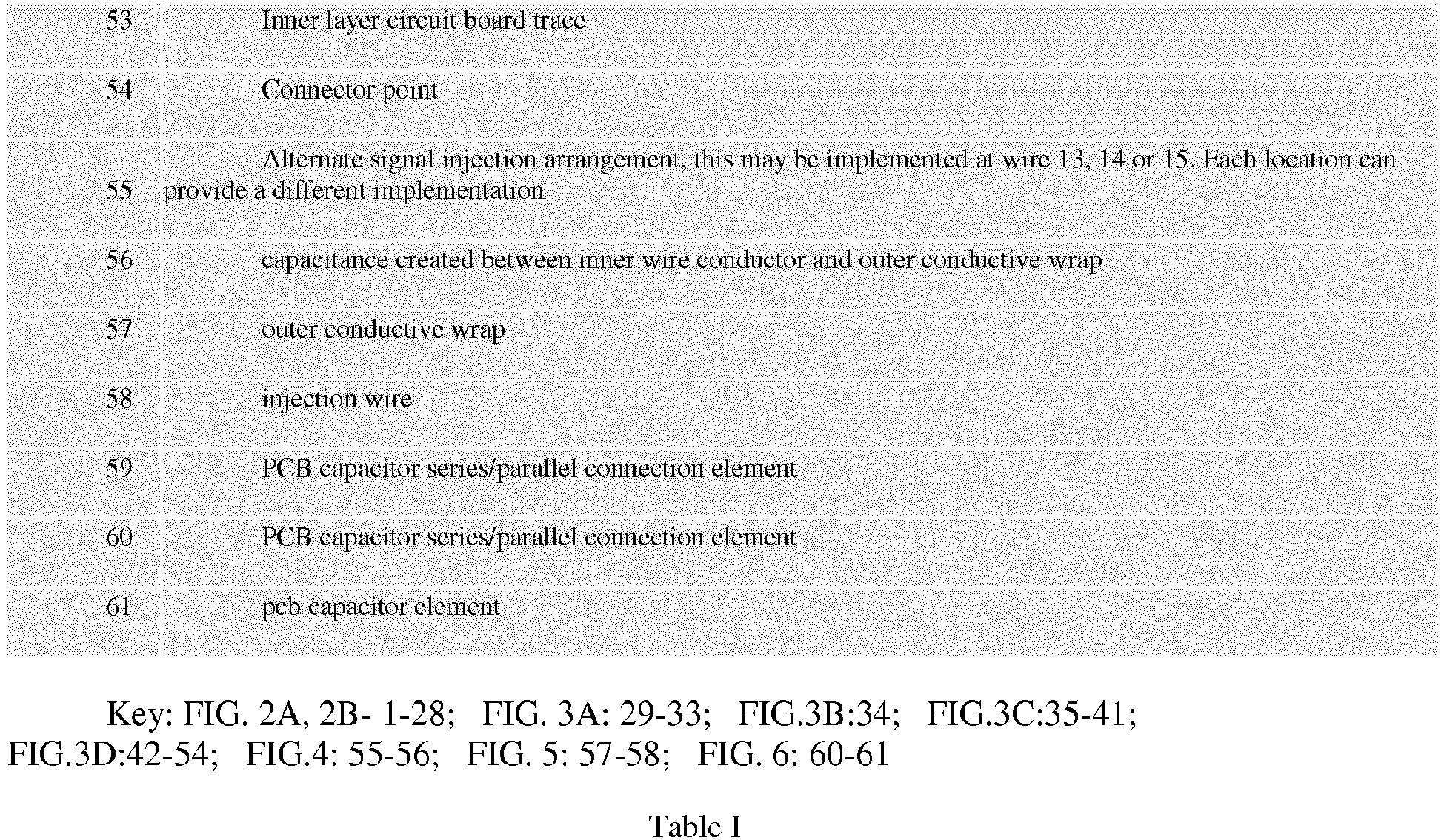
- a listing of components for certain figures to follow is provided in Table I.
- the protection arrangement 200 is shown in relation to a transformer, where the transformer secondary 18 is shown in three phases that are connected to NGR protective earth connection point 10.
- a neutral grounding resistor 8 is connected to a node 10 between wire 15 and wire 14, as may be the case in known arrangements.
- the current transformer 20 is used to sense current along the wire 14 with the aid of burden resistor measurement point 26, facilitating measurement of current at node 9 for the neutralizing ground resistor 8.
- a sense circuit is configured as a sensing resistor assembly 19, including a sensing resistor diode assembly 3, a sense resistor 2, and an injection capacitor 1, arranged in electrical series between the neutral grounding resistor 8 and an NGR monitor device 21.
- the NGR monitor device in turn, incudes a signal processing circuit 28, and injection signal generator 27, arranged to generate a high frequency signal through injection capacitor 1, such as kHz or MHz signal, or GHz signal.
- injection capacitor 1 such as kHz or MHz signal, or GHz signal.
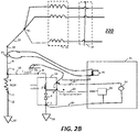
- capacitor arrangement 55 shown in the protection arrangement 220 of FIG. 2B , the injection capacitor 1, may be located to directly connect to wire 13 (as shown), wire 14, or wire 15.
- the protection arrangement 200 may probe the resistance of neutral grounding resistor 8 intermittently, regularly, or upon request, by sending an injection signal from the injection signal generator 27.
- FIGs. 7A-7E depicts exemplary waveforms for implementing embodiments of the present disclosure. Suitable waveforms include sinusoidal shape, pulse shape, triangle shape, square wave shape, or arbitrary. The present inventors have determined that small changes in resistance of a neutral grounding resistor presenting resistance in the range of tens of Ohms may readily be measured using an arrangement generally as shown in FIG. 2 , where the signal frequency is in the 100-kHz range. The embodiments are not limited in this context. FIG.
- resistor 8 presents exemplary data for a resistor coupled to an injection capacitor having capacitance of 1 nF, showing impedance as a function of frequency.
- resistance changes in the range of 1 Ohm may be readily detected during operation of a signal injector circuit in the 100 kHz to 1MHz range.
- neutral grounding resistors having a nominal resistance of 50 Ohm as an example such resistance changes fall well below certain operation specifications, where the resistance is to be maintained within a 20% of nominal value.
- an injection capacitor may be implemented in different configurations.
- FIG. 3A presents one embodiment of a capacitor 29, embodied as wire with a conductive outer wall wrapped around the exterior according to the present embodiments.
- a wire element 30 is wrapped by wire insulation 31, and a conductive outer wrap 32A.
- a signal injection wire 32B connects to the conductive outer wrap 32A, with another wire element 33 on the other side of the conductive outer wrap 32A.
- FIG. 3B presents another embodiment of a capacitor 34 according to the present embodiments.
- the capacitor 34 may be a known capacitor, such as a parallel plate capacitor or any convenient "off the shelf' capacitor arranged with the appropriate capacitance.
- FIG. 3C presents a further embodiment of a capacitor 35 according to the present embodiments.
- the capacitor 35 is a two-layer printed circuit board (PCB) capacitor, arranged with a first connection point 36 and a second connection point 41.
- the printed circuit board may have a printed circuit board body composed of a known material, such as FR4.
- a first outer layer circuit board trace 37 is arranged on one side, while a second outer layer circuit board trace is arranged on the other side of the capacitor formed by a circuit board dielectric 38.
- the effective capacitance presented by the circuit board dielectric is represented by capacitor 39.
- the area (in plan view of the capacitor 35) as well as the thickness (between outer layer circuit board traces) and dielectric permittivity of the circuit board dielectric may be adjusted independently of one another.
- FIG. 3D presents an additional embodiment of a capacitor 42, according to the present embodiments.
- the capacitor 42 is arranged as a multi-layer PCB capacitor, based upon a circuit board dielectric 45.
- An outer layer circuit board trace 43 is provided on the top of the capacitor, while an inner layer circuit board trace 44 is shown below the outer layer circuit board trace 43.
- Various additional inner layer circuit board traces and connection points are provided in the capacitor 42, as shown, and detailed in table I.
- the various traces may be formed of known metal layers, such as copper. Some of the traces may be electrically conductively connected to one another such as 43, 46, 49, while other traces are electrically conductively connected to one another, such as 54, 53, 50, using plated vias.
- the coupled traces may form a capacitor whose area exceeds the planar area of the circuit board.
- three traces that occupy the full area of the PCB may exhibit a capacitor area approximately 3 times the area of the PCB.
- the capacitor 42 provides a convenient configuration to generate high capacitance in a relatively smaller area.
- FIG. 4 presents details of a capacitor arrangement 55, where the capacitor 56 represents a capacitance created between an inner wire conductor and outer conductive wrap, as detailed at FIG. 5 .
- an injection wire 58 (coupled to a signal injector) is electrically connected to a wire wrap 57, disposed around a wire between nodes 9 and 10.
- FIG. 6 shows a further capacitor arrangement, according to embodiments of the disclosure.
- multiple capacitors may be built in each PCB, where capacitors are electrically connected to fulfill target properties, such as stand-off voltage, total capacitance, parasitic loss, reliability, and manufacturing limitations.
- FIG. 9 depicts a protection arrangement 300, according to further embodiments of the disclosure.
- the protection arrangement 300 involves capacitive coupling of an inspection signal to measure the resistance of neutral grounding resistor 8.
- the protection arrangement 300 includes a current transformer 301, capable of operating at the frequencies of interest, as well as a signal source 302, to excite a secondary end of the current transformer 301.
- the current transformer 301 may be located at different locations in the protection arrangement 300, as indicated by reference number 303.
- the location of different voltage measurements (V Ud) is also shown.
- the protection arrangement 300 also includes a capacitor 304, which capacitor generates a high frequency path to complete the electrical circuit around the neutral grounding resistor 8. This arrangement provides greater isolation to the control electronics and if coupled directly across an NGR, provides even better measurement accuracy.
- FIG. 10 depicts an exemplary process flow 1000.
- a power system is connected to a fault protection arrangement.
- the fault protection arrangement may include a neutral grounding resistor, the neutral grounding resistor comprising a ground end and a non-ground end; a sense circuit, coupled to the non-ground end of the neutral grounding resistor, the sense circuit comprising a sense resistor, and an injection capacitor; and an injection signal generator, coupled to the non-ground end of the neutral grounding resistor.
- a resistance of the neutral grounding resistor is probed by sending an injection signal from the sense circuit.
- an alarm signal is generated when the resistance of the neutral grounding resistor falls outside of a predetermined range.
- the present embodiments provide components, circuit arrangements and techniques to conveniently monitor small changes in resistance, such as in neutral grounding resistors.
- System implementations may be realized by injecting a high frequency signal through a neutralizing wire with a capacitor arranged such as in FIG. 5 .
- an injecting capacitor may be collocated with sensing resistor in a sense circuit.
- an injecting capacitor may be embodied in a PCB, including in a multilayer PCB having 4 layers, 6 layers, 8 layers, and so forth.
Landscapes
- Physics & Mathematics (AREA)
- General Physics & Mathematics (AREA)
- Testing Of Short-Circuits, Discontinuities, Leakage, Or Incorrect Line Connections (AREA)
- Measurement Of Resistance Or Impedance (AREA)
- Emergency Protection Circuit Devices (AREA)
- Monitoring And Testing Of Exchanges (AREA)
- Amplifiers (AREA)
Abstract
Description
- The disclosure relates to the field of protection devices, and in particular, to neutral grounding resistors.
- Ground fault resistors, or neutral grounding resistors, may be used in conjunction with resistance grounded power systems. A neutral grounding resistor may be deployed under conditions where a ground fault is to be limited to a predetermined current. Neutral grounding resistors may also be accompanied by a monitor to monitor when degradation of neutral grounding resistor may take place. In some jurisdictions, monitoring of neutral grounding resistors is required during all operation phases for changes in resistance value.
- In view of the above, the present embodiments are provided.
- In one embodiment, a fault protection arrangement may include a neutral grounding resistor, the neutral grounding resistor comprising a ground end and a non-ground end. The arrangement may further include a sense circuit, coupled to the non-ground end of the neutral grounding resistor. The arrangement may include an injection signal generator, coupled to the non-ground end of the neutral grounding resistor, the injection signal generator arranged to generate a frequency of 240 Hz or greater.
- In another embodiment, a neutral grounding resistor monitor assembly is provided. The neutral grounding resistor monitor assembly may include a sense resistor circuit, having an output, arranged to connect to a non-ground end of a neutral grounding resistor and an injection signal generator, arranged to connect to the non-ground end of the neutral grounding resistor, the injection signal generator arranged to generate an alternating current signal. The neutral grounding resistor monitor assembly may further include an injection capacitor, the injection capacitor comprising a first electrode coupled to receive a signal from the injection signal generator, and a second electrode, arranged to connect to the non-ground end of the neutral grounding resistor.
- In another embodiment, a fault protection method may include connecting a power system to a fault protection arrangement. The fault protection arrangement may include a neutral grounding resistor, the neutral grounding resistor comprising a ground end and a non-ground end; a sense circuit, coupled to the non-ground end of the neutral grounding resistor, the sense circuit comprising a sense resistor, and an injection capacitor. The fault protection arrangement may include an injection signal generator, coupled to the non-ground end of the neutral grounding resistor. The method may also include probing a resistance of the neutral grounding resistor by sending an injection signal from the sense circuit.
-
-
FIG. 1A shows a protection arrangement according to various embodiments of the disclosure; -
FIG. 1B shows a further protection arrangement according to various embodiments of the disclosure; -
FIG. 1C shows another protection arrangement according to various embodiments of the disclosure; -
FIG. 1D shows yet another protection arrangement according to various embodiments of the disclosure; -
FIG. 2A shows another protection arrangement in accordance to additional embodiments of the disclosure; -
FIG. 2B shows another protection arrangement in accordance to additional embodiments of the disclosure; -
FIG. 3A presents one embodiment of a capacitor according to the present embodiments; -
FIG. 3B presents another embodiment of a capacitor according to the present embodiments; -
FIG. 3C presents a further embodiment of a capacitor according to the present embodiments; -
FIG. 3D presents an additional embodiment of a capacitor according to the present embodiments; -
FIG. 4 depicts a capacitor arrangement, according to embodiments of the disclosure; and -
FIG. 5 presents a perspective view of an additional embodiment of a capacitor according to the present embodiments; -
FIG. 6 shows a further capacitor arrangement, according to embodiments of the disclosure; -
FIGs. 7A-7E depicts exemplary waveforms for implementing embodiments of the present disclosure; -
FIG. 8 depicts exemplary measurement results showing high frequency impedance measurements resulting from small changes in resistance in a grounding resistor; -
FIG. 9 depicts an exemplary protection arrangement, according to further embodiments of the disclosure; and -
FIG. 10 depicts an exemplary process flow. - The present embodiments will now be described more fully hereinafter with reference to the accompanying drawings, in which exemplary embodiments are shown. The embodiments are not to be construed as limited to the embodiments set forth herein. Rather, these embodiments are provided so that this disclosure will be thorough and complete, and will fully convey their scope to those skilled in the art. In the drawings, like numbers refer to like elements throughout.
- In the following description and/or claims, the terms "on," "overlying,", "disposed on" and "over" may be used in the following description and claims. "On" "overlying" ,"disposed on" and "over" may be used to indicate that two or more elements are in direct physical contact with one another. Also, the term "on", "overlying", "disposed on," and "over", may mean that two or more elements are not in direct contact with one another. For example, "over" may mean that one element is above another element while not contacting one another and may have another element or elements in between the two elements. Furthermore, the term "and/or" may mean "and", it may mean "or", it may mean "exclusive-or", it may mean "one", it may mean "some, but not all", it may mean "neither", and/or it may mean "both", although the scope of claimed subject matter is not limited in this respect.
- In various embodiments, systems and devices are provided for providing fault protection.
FIG. 1A shows afault protection arrangement 150 according to various embodiments of the disclosure. Thefault protection arrangement 150 includes aneutral grounding resistor 158, coupled on a non-ground end to a neutral groundingresistor monitor assembly 152. The neutral groundingresistor monitor assembly 152 may include asignal generator 154 and asense circuit 156, where variants of this arrangement are described in more detail with respect to the figures to follow.FIG. 1B shows anotherfault protection arrangement 160 according to various embodiments of the disclosure. Thefault protection arrangement 160 includes aneutral grounding resistor 158, coupled on a non-ground end to a neutral groundingresistor monitor assembly 162. The neutral groundingresistor monitor assembly 162 may include asignal generator 154 and asense circuit 156, and acapacitor 164, disposed between the sense circuit and non-grounding end of theneutral grounding resistor 158, where variants of this arrangement are described in more detail with respect to the figures to follow.FIG. 1C shows a furtherfault protection arrangement 170 according to various embodiments of the disclosure. Thefault protection arrangement 170 includes aneutral grounding resistor 158, coupled on a non-ground end to a neutral groundingresistor monitor assembly 172. The neutral groundingresistor monitor assembly 172 may include aninjection signal generator 154 and asense circuit 156,capacitor 164, disposed between theinjection signal generator 154 and non-grounding end of theneutral grounding resistor 158, andcapacitor 176, disposed between thesense circuit 156 andneutral grounding resistor 158, where variants of this arrangement are described in more detail with respect to the figures to follow. - FIG. ID shows a
fault protection arrangement 100 according to various embodiments of the disclosure. Thefault protection arrangement 100 involves aneutral grounding resistor 102, electrically coupled to ground and coupled to apower system 130. Thepower system 130 may include various known components including transformers and other equipment. Theneutral grounding resistor 102 may be designed to provide a target resistance over any suitable range, such as 10 Ω to thousands of Ω. The embodiments are not limited in this context. During operation, theneutral grounding resistor 102 is designed to present a fixed electrical resistance, to treat a given fault energy received, for example, over a line between the neutral grounding resistor andpower system 130. In particular, theneutral grounding resistor 102 may be coupled to the neutral of a power system to limit fault current, providing a path for grounding current to a transformer neutral. Excessive changes in the resistance value of theneutral grounding resistor 102 may cause harm to a system being protected. In accordance with embodiments of the disclosure, thefault protection arrangement 100 provides monitoring and control to determine the state of theneutral grounding resistor 102. - The
fault protection arrangement 100 includes asense circuit 110 andsignal generation circuit 120, acting together as a neutral grounding resistor monitor for theneutral grounding resistor 102. Thesignal generation circuit 120 may includeinjection signal generator 122, while the sense circuit includescapacitor 112. Theinjection signal generator 122 may operate at the kHz to GHz range in various non-limiting embodiments. Advantageously, theinjection signal generator 122 may operate below approximately 1 MHz in some embodiments. In operation, a high frequency signal of any suitable waveform is sent by theinjection signal generator 122 to theneutral grounding resistor 102 along an electrical path including thecapacitor 112. Thecapacitor 112 may be sized to exhibit an appropriate capacitance and breakdown voltage according to the system to be protected. Particularly, thecapacitor 112 may exhibit a capacitance of hundreds of picoFarads, nanoFarads, to hundreds of nanoFarads. By use of suitable capacitance for thecapacitor 112 at an appropriate probe frequency, such as 300 kHz, small changes in impedance of theneutral ground resistor 102 may be ascertained, as detailed in the embodiments to follow. - In some embodiments, the repetition frequency of the
injection signal generator 122 may range from 240 Hz to 10 MHz, while the edge rate range from 240 Hz to 10 GHz. In particular embodiments, the repetition rate may range from 100 kHz to 5 MHz, while the edge rate ranged from 100 kHz to 1 GHz. The signals generated byinjection signal generator 122 may be used to probe resistance of a neutral grounding resistor in open state, short circuit state, or a changing value under normal operation. In addition, system inductance, NGR inductance, connection inductance, system capacitance, NGR capacitance, and connection capacitance may be probed by the signals. - As further shown in FIG. ID, the signal generation circuit may further include an
alarm circuit 124, to generate an alarm signal when the resistance of theneutral grounding resistor 102 falls outside of a predetermined range. -
FIG. 2A shows aprotection arrangement 200 according to additional embodiments of the disclosure. A listing of components for certain figures to follow is provided in Table I.


- The
protection arrangement 200 is shown in relation to a transformer, where the transformer secondary 18 is shown in three phases that are connected to NGR protectiveearth connection point 10. Aneutral grounding resistor 8 is connected to anode 10 betweenwire 15 andwire 14, as may be the case in known arrangements. Thecurrent transformer 20 is used to sense current along thewire 14 with the aid of burdenresistor measurement point 26, facilitating measurement of current atnode 9 for the neutralizingground resistor 8. In this embodiment a sense circuit is configured as asensing resistor assembly 19, including a sensingresistor diode assembly 3, asense resistor 2, and aninjection capacitor 1, arranged in electrical series between theneutral grounding resistor 8 and anNGR monitor device 21. The NGR monitor device, in turn, incudes asignal processing circuit 28, andinjection signal generator 27, arranged to generate a high frequency signal throughinjection capacitor 1, such as kHz or MHz signal, or GHz signal. In onevariant capacitor arrangement 55, shown in theprotection arrangement 220 ofFIG. 2B , theinjection capacitor 1, may be located to directly connect to wire 13 (as shown),wire 14, orwire 15. - In operation, the
protection arrangement 200 may probe the resistance ofneutral grounding resistor 8 intermittently, regularly, or upon request, by sending an injection signal from theinjection signal generator 27.FIGs. 7A-7E depicts exemplary waveforms for implementing embodiments of the present disclosure. Suitable waveforms include sinusoidal shape, pulse shape, triangle shape, square wave shape, or arbitrary. The present inventors have determined that small changes in resistance of a neutral grounding resistor presenting resistance in the range of tens of Ohms may readily be measured using an arrangement generally as shown inFIG. 2 , where the signal frequency is in the 100-kHz range. The embodiments are not limited in this context.FIG. 8 presents exemplary data for a resistor coupled to an injection capacitor having capacitance of 1 nF, showing impedance as a function of frequency. As such, resistance changes in the range of 1 Ohm may be readily detected during operation of a signal injector circuit in the 100 kHz to 1MHz range. For neutral grounding resistors having a nominal resistance of 50 Ohm as an example, such resistance changes fall well below certain operation specifications, where the resistance is to be maintained within a 20% of nominal value. - In addition to modifying waveform shape, scanning an installation with a frequency sweep can determine optimal frequency and installation parasitic losses. Moreover, a search algorithm may be implemented to find optimal frequencies for the system installation. In accordance with various embodiments of the disclosure, an injection capacitor may be implemented in different configurations.
-
FIG. 3A presents one embodiment of acapacitor 29, embodied as wire with a conductive outer wall wrapped around the exterior according to the present embodiments. Awire element 30 is wrapped bywire insulation 31, and a conductiveouter wrap 32A. Asignal injection wire 32B connects to the conductiveouter wrap 32A, with anotherwire element 33 on the other side of the conductiveouter wrap 32A. -
FIG. 3B presents another embodiment of acapacitor 34 according to the present embodiments. Here, thecapacitor 34 may be a known capacitor, such as a parallel plate capacitor or any convenient "off the shelf' capacitor arranged with the appropriate capacitance. -
FIG. 3C presents a further embodiment of acapacitor 35 according to the present embodiments. In this embodiment, thecapacitor 35 is a two-layer printed circuit board (PCB) capacitor, arranged with afirst connection point 36 and asecond connection point 41. The printed circuit board may have a printed circuit board body composed of a known material, such as FR4. A first outer layercircuit board trace 37 is arranged on one side, while a second outer layer circuit board trace is arranged on the other side of the capacitor formed by acircuit board dielectric 38. The effective capacitance presented by the circuit board dielectric is represented bycapacitor 39. To achieve a target capacitance, the area (in plan view of the capacitor 35) as well as the thickness (between outer layer circuit board traces) and dielectric permittivity of the circuit board dielectric may be adjusted independently of one another. -
FIG. 3D presents an additional embodiment of acapacitor 42, according to the present embodiments. Here, thecapacitor 42 is arranged as a multi-layer PCB capacitor, based upon acircuit board dielectric 45. An outer layercircuit board trace 43 is provided on the top of the capacitor, while an inner layercircuit board trace 44 is shown below the outer layercircuit board trace 43. Various additional inner layer circuit board traces and connection points are provided in thecapacitor 42, as shown, and detailed in table I. The various traces may be formed of known metal layers, such as copper. Some of the traces may be electrically conductively connected to one another such as 43, 46, 49, while other traces are electrically conductively connected to one another, such as 54, 53, 50, using plated vias. As such, the coupled traces may form a capacitor whose area exceeds the planar area of the circuit board. For example, three traces that occupy the full area of the PCB may exhibit a capacitor area approximately 3 times the area of the PCB. Thus, thecapacitor 42 provides a convenient configuration to generate high capacitance in a relatively smaller area. -
FIG. 4 presents details of acapacitor arrangement 55, where thecapacitor 56 represents a capacitance created between an inner wire conductor and outer conductive wrap, as detailed atFIG. 5 . As shown, an injection wire 58 (coupled to a signal injector) is electrically connected to awire wrap 57, disposed around a wire betweennodes -
FIG. 6 shows a further capacitor arrangement, according to embodiments of the disclosure. In this arrangement, multiple capacitors may be built in each PCB, where capacitors are electrically connected to fulfill target properties, such as stand-off voltage, total capacitance, parasitic loss, reliability, and manufacturing limitations. -
FIG. 9 depicts aprotection arrangement 300, according to further embodiments of the disclosure. Theprotection arrangement 300 involves capacitive coupling of an inspection signal to measure the resistance ofneutral grounding resistor 8. Theprotection arrangement 300 includes acurrent transformer 301, capable of operating at the frequencies of interest, as well as asignal source 302, to excite a secondary end of thecurrent transformer 301. In different embodiments, thecurrent transformer 301 may be located at different locations in theprotection arrangement 300, as indicated byreference number 303. The location of different voltage measurements (V Ud) is also shown. Theprotection arrangement 300 also includes acapacitor 304, which capacitor generates a high frequency path to complete the electrical circuit around theneutral grounding resistor 8. This arrangement provides greater isolation to the control electronics and if coupled directly across an NGR, provides even better measurement accuracy. -
FIG. 10 depicts anexemplary process flow 1000. At 1002, a power system is connected to a fault protection arrangement. According to various embodiments, the fault protection arrangement may include a neutral grounding resistor, the neutral grounding resistor comprising a ground end and a non-ground end; a sense circuit, coupled to the non-ground end of the neutral grounding resistor, the sense circuit comprising a sense resistor, and an injection capacitor; and an injection signal generator, coupled to the non-ground end of the neutral grounding resistor. Atblock 1004, a resistance of the neutral grounding resistor is probed by sending an injection signal from the sense circuit. Atblock 1006, an alarm signal is generated when the resistance of the neutral grounding resistor falls outside of a predetermined range. - In sum, the present embodiments provide components, circuit arrangements and techniques to conveniently monitor small changes in resistance, such as in neutral grounding resistors. System implementations may be realized by injecting a high frequency signal through a neutralizing wire with a capacitor arranged such as in
FIG. 5 . Alternatively, an injecting capacitor may be collocated with sensing resistor in a sense circuit. In various embodiments, an injecting capacitor may be embodied in a PCB, including in a multilayer PCB having 4 layers, 6 layers, 8 layers, and so forth. - While the present embodiments have been disclosed with reference to certain embodiments, numerous modifications, alterations and changes to the described embodiments are possible while not departing from the sphere and scope of the present disclosure, as defined in the appended claims. Accordingly, the present embodiments are not to be limited to the described embodiments, and may have the full scope defined by the language of the following claims, and equivalents thereof.
Claims (15)
- A fault protection arrangement, comprising:a neutral grounding resistor, the neutral grounding resistor comprising a ground end and a non-ground end;and a neutral grounding resistance monitor assembly, comprising:a sense circuit, coupled to the non-ground end of the neutral grounding resistor; andan injection signal generator, coupled to the non-ground end of the neutral grounding resistor the injection signal generator arranged to generate a frequency of 240 Hz or greater.
- The fault protection arrangement of claim 1, further comprising:
a capacitor, having a first electrode coupled to receive a signal from the injection signal generator, and a second electrode, coupled to the non-ground end of the neutral grounding resistor. - The fault protection arrangement of claim 2, wherein the capacitor comprises:a conductive wire, coupled to the non-ground end of the neutral grounding resistor; andconductive wrap, concentrically disposed around the conductive wire, and coupled to receive a signal from the injection signal generator.
- The fault protection arrangement of claim 2 or 3, wherein the capacitor comprises:a printed circuit board body;a first conductive trace, disposed on a first surface of the printed circuit board body, and covering a majority of the first surface; anda second conductive trace, disposed one a second surface of the printed circuit board body, and covering a majority of the second surface, opposite the first surface,preferably wherein the capacitor further comprises:a third conductive trace, disposed within the printed circuit board body, and electrically conductively connected to the first conductive trace; anda fourth conductive trace, disposed within the printed circuit board body, and electrically conductively connected to the second conductive trace,wherein a capacitor area of the capacitor exceeds a planar area of the printed circuit board body.
- The fault protection arrangement of any of the preceding claims with one or more of the following:wherein the injection signal generator is arranged to generate a frequency of 1 MHz or less;wherein the neutral grounding resistor comprises a signal processing circuit,connected to the injection signal generator;wherein the sense circuit comprises a sensing resistor diode assembly, a sense resistor, and an injection capacitor.
- The fault protection arrangement of any of the preceding claims, wherein the injection signal generator is configured to generate a waveform having a shape chosen from one of: sinusoidal shape, pulse shape, triangle shape, square wave shape, or arbitrary shape.
- The fault protection arrangement of any of the preceding claims, wherein the injection signal comprises a signal frequency in a100-kHz to 900 kHz range.
- A neutral grounding resistor monitor assembly, comprising:a sense resistor circuit, having an output, arranged to connect to a non-ground end of a neutral grounding resistor;an injection signal generator, arranged to connect to the non-ground end of the neutral grounding resistor the injection signal generator arranged to generate an alternating current signal; andan injection capacitor, the injection capacitor comprising a first electrode coupled to receive a signal from the injection signal generator, and a second electrode, arranged to connect to the non-ground end of the neutral grounding resistor.
- The neutral grounding resistor monitor assembly of claim 8 with one or more of the following:wherein the injection capacitor is included in the sense resistor circuit;wherein the alternating current signal comprises a signal frequency in a 100 kHz to 900 kHz range.
- The neutral grounding resistor monitor assembly of claim 8 or 9, wherein the injection capacitor comprises:a conductive wire, coupled to the non-ground end of the neutral grounding resistor; andconductive wrap, concentrically disposed around the conductive wire, and coupled to receive a signal from the injection signal generator.
- The neutral grounding resistor monitor assembly of any of the claims 8-10, wherein the injection capacitor comprises:a printed circuit board body;a first conductive trace, disposed on a first surface of the printed circuit board body, and covering a majority of the first surface; anda second conductive trace, disposed one a second surface of the printed circuit board body, and covering a majority of the second surface, opposite the first surface.
- The neutral grounding resistor monitor assembly of claim 11, wherein the injection capacitor comprises:a third conductive trace, disposed within the printed circuit board body, and electrically conductively connected to the first conductive trace; anda fourth conductive trace, disposed within the printed circuit board body, and electrically conductively connected to the second conductive trace,wherein a capacitor area of the capacitor exceeds a planar area of the printed circuit board body.
- The neutral grounding resistor monitor assembly of any of the claims 8-12, wherein the neutral grounding resistor monitor comprises an alarm circuit, to generate an alarm signal when the resistance of the neutral grounding resistor falls outside of a predetermined range.
- A fault protection method, comprising:connecting a power system to a fault protection arrangement, the fault protection arrangement comprising:a neutral grounding resistor, the neutral grounding resistor comprising a ground end and a non-ground end; anda neutral grounding resistor monitor assembly, comprising:a sense circuit, coupled to the non-ground end of the neutral grounding resistor, the sense circuit comprising a sense resistor, and an injection capacitor; andan injection signal generator, coupled to the non-ground end of the neutral grounding resistor; andprobing a resistance of the neutral grounding resistor by sending an injection signal from the sense circuit.
- The method of claim 14, wherein a frequency of the injection signal ranges from 240 Hz to 10 MHz, and wherein an edge rate of the injection signal ranges from 240 Hz to 10 GHz, and/or wherein the injection signal comprises a waveform having a shape chosen from one of: sinusoidal shape, pulse shape, triangle shape, square wave shape, or arbitrary shape.
Applications Claiming Priority (2)
| Application Number | Priority Date | Filing Date | Title |
|---|---|---|---|
| US201862644359P | 2018-03-16 | 2018-03-16 | |
| US16/297,487 US11108222B2 (en) | 2018-03-16 | 2019-03-08 | Monitor device, ground fault protection circuit and techniques |
Publications (2)
| Publication Number | Publication Date |
|---|---|
| EP3540890A1 true EP3540890A1 (en) | 2019-09-18 |
| EP3540890B1 EP3540890B1 (en) | 2024-06-26 |
Family
ID=65818238
Family Applications (1)
| Application Number | Title | Priority Date | Filing Date |
|---|---|---|---|
| EP19163284.3A Active EP3540890B1 (en) | 2018-03-16 | 2019-03-15 | Monitor device, ground fault protection circuit and techniques |
Country Status (5)
| Country | Link |
|---|---|
| US (1) | US11108222B2 (en) |
| EP (1) | EP3540890B1 (en) |
| AU (1) | AU2019201769B2 (en) |
| CA (1) | CA3036728C (en) |
| ES (1) | ES2985402T3 (en) |
Families Citing this family (5)
| Publication number | Priority date | Publication date | Assignee | Title |
|---|---|---|---|---|
| CN112368585A (en) * | 2018-05-28 | 2021-02-12 | 以斯拉·舒库里 | Ground wire monitoring tester |
| JP7770916B2 (en) * | 2018-09-28 | 2025-11-17 | テックホールド・エルエルシー | Power grid protection via transformer neutral interruption systems and triggered phase disconnection |
| US11368014B2 (en) * | 2020-05-18 | 2022-06-21 | Littelfuse, Inc. | Ground fault protection circuit and techniques |
| CN112505431A (en) * | 2020-12-28 | 2021-03-16 | 广东电网有限责任公司 | Method and device for determining mutual inductance coupling component between grounding impedance test lines |
| CN116316428A (en) * | 2021-12-09 | 2023-06-23 | 国家电投集团黄河上游水电开发有限责任公司 | A neutral point linear grounding resistance cabinet on the low-voltage side of a transformer |
Citations (6)
| Publication number | Priority date | Publication date | Assignee | Title |
|---|---|---|---|---|
| US5508620A (en) * | 1993-09-01 | 1996-04-16 | Abb Management Ag | Method and device for determining ground faults on the conductors of an electrical machine |
| JP2002131361A (en) * | 2000-10-23 | 2002-05-09 | Koha Co Ltd | Wiring short circuit detecting device |
| US7180300B2 (en) * | 2004-12-10 | 2007-02-20 | General Electric Company | System and method of locating ground fault in electrical power distribution system |
| US8405940B2 (en) * | 2009-10-13 | 2013-03-26 | Schweitzer Engineering Laboratories Inc | Systems and methods for generator ground fault protection |
| US20140153142A1 (en) * | 2011-05-31 | 2014-06-05 | Abb Schweiz Ag | Ground fault protection |
| EP2772770A1 (en) * | 2013-02-28 | 2014-09-03 | Alstom Technology Ltd | Rotor earth fault protection for an electrical variable speed doubly fed induction machine |
Family Cites Families (22)
| Publication number | Priority date | Publication date | Assignee | Title |
|---|---|---|---|---|
| US3848159A (en) * | 1973-06-18 | 1974-11-12 | Airpax Electronics | Ground fault detector circuit with feedback to sensor |
| CH579840A5 (en) | 1974-11-14 | 1976-09-15 | Bbc Brown Boveri & Cie | |
| SE462244B (en) | 1988-09-21 | 1990-05-21 | Asea Brown Boveri | ELECTRO-LINE PROTECTION FOR EARTH ERROR DETECTION |
| FR2783926B1 (en) * | 1998-09-28 | 2001-10-19 | Socrat | METHOD AND DEVICE FOR LOCATING A CABLE ISOLATION DEFECT |
| JP4061168B2 (en) * | 2002-10-16 | 2008-03-12 | 矢崎総業株式会社 | Ground fault detection device and insulation resistance measurement device |
| JP2007198995A (en) * | 2006-01-30 | 2007-08-09 | Matsushita Electric Ind Co Ltd | Ground fault resistance measurement circuit and ground fault detection circuit |
| US7852089B2 (en) * | 2008-05-08 | 2010-12-14 | Lear Corporation | Ground-fault detection system for vehicles with a high-voltage power net |
| EP2230522B1 (en) * | 2009-03-16 | 2011-05-11 | SMA Solar Technology AG | Method and device for insulation monitoring of a network without a neutral conductor |
| US8760170B2 (en) | 2011-01-28 | 2014-06-24 | Schneider Electric Solar Inverters Usa, Inc. | Fuse continuity detection |
| FR2975498B1 (en) * | 2011-05-19 | 2014-02-14 | Renault Sa | DEVICE AND METHOD FOR ESTIMATING THE RESISTANCE OF EARTH CONNECTION OF AN ELECTRICAL APPARATUS |
| EP2837076B1 (en) * | 2012-04-12 | 2017-10-04 | Littelfuse, Inc. | Neutral grounding resistor monitor |
| CN103472404A (en) * | 2012-06-06 | 2013-12-25 | 鸿富锦精密工业(深圳)有限公司 | Grounding detection circuit |
| JP5631444B1 (en) * | 2013-05-27 | 2014-11-26 | タナシン電機株式会社 | Leakage current calculation device and leakage current calculation method |
| US10291017B2 (en) * | 2013-06-07 | 2019-05-14 | Iep2 Research Pty Limited | Electrical protection device and a method of providing electrical protection |
| US9547032B2 (en) * | 2013-08-29 | 2017-01-17 | Intermountain Electronics, Inc. | Frequency hopping ground monitor current sensing |
| US9541595B2 (en) * | 2013-08-29 | 2017-01-10 | Intermountain Electronics, Inc. | Multi-frequency ground monitor current sensing |
| US9541596B2 (en) * | 2013-08-29 | 2017-01-10 | Intermountain Electronics, Inc. | Multi-frequency ground monitor current sensing without a DC component |
| KR102066035B1 (en) * | 2013-12-12 | 2020-01-14 | 온세미컨덕터코리아 주식회사 | Sensing resistor short determination circuit, and switch control circuit and power supply comprising the same |
| US9488689B2 (en) * | 2014-08-28 | 2016-11-08 | General Electric Company | Systems and methods for identifying fault location using distributed communication |
| US10141142B2 (en) * | 2015-11-12 | 2018-11-27 | Intermountain Electronics, Inc. | Multiple frequency tone monitor |
| KR101737072B1 (en) * | 2016-07-13 | 2017-05-18 | 선광엘티아이(주) | Resistance and current observation system of the ground line |
| CN106707087B (en) * | 2017-02-04 | 2024-04-05 | 山西全安新技术开发有限公司 | Underground electrical equipment grounding monitoring method and system |
-
2019
- 2019-03-08 US US16/297,487 patent/US11108222B2/en active Active
- 2019-03-14 CA CA3036728A patent/CA3036728C/en active Active
- 2019-03-14 AU AU2019201769A patent/AU2019201769B2/en active Active
- 2019-03-15 ES ES19163284T patent/ES2985402T3/en active Active
- 2019-03-15 EP EP19163284.3A patent/EP3540890B1/en active Active
Patent Citations (6)
| Publication number | Priority date | Publication date | Assignee | Title |
|---|---|---|---|---|
| US5508620A (en) * | 1993-09-01 | 1996-04-16 | Abb Management Ag | Method and device for determining ground faults on the conductors of an electrical machine |
| JP2002131361A (en) * | 2000-10-23 | 2002-05-09 | Koha Co Ltd | Wiring short circuit detecting device |
| US7180300B2 (en) * | 2004-12-10 | 2007-02-20 | General Electric Company | System and method of locating ground fault in electrical power distribution system |
| US8405940B2 (en) * | 2009-10-13 | 2013-03-26 | Schweitzer Engineering Laboratories Inc | Systems and methods for generator ground fault protection |
| US20140153142A1 (en) * | 2011-05-31 | 2014-06-05 | Abb Schweiz Ag | Ground fault protection |
| EP2772770A1 (en) * | 2013-02-28 | 2014-09-03 | Alstom Technology Ltd | Rotor earth fault protection for an electrical variable speed doubly fed induction machine |
Also Published As
| Publication number | Publication date |
|---|---|
| US20190288499A1 (en) | 2019-09-19 |
| AU2019201769B2 (en) | 2023-09-21 |
| AU2019201769A1 (en) | 2019-10-03 |
| US11108222B2 (en) | 2021-08-31 |
| EP3540890B1 (en) | 2024-06-26 |
| ES2985402T3 (en) | 2024-11-05 |
| CA3036728A1 (en) | 2019-09-16 |
| CA3036728C (en) | 2024-03-19 |
Similar Documents
| Publication | Publication Date | Title |
|---|---|---|
| CA3036728C (en) | Monitor device, ground fault protection circuit and techniques | |
| US5323117A (en) | Method for detecting partial discharge in an insulation of an electric power apparatus | |
| EP3143416B1 (en) | A partial discharge acquisition system comprising a capacitive coupling electric field sensor | |
| US6980174B2 (en) | Process control instrument intrinsic safety barrier | |
| KR102811866B1 (en) | IC noise tolerance detection device and IC noise tolerance detection method | |
| TW200944808A (en) | Partial discharge measuring method | |
| MX2011012925A (en) | Impedance-based current sensor. | |
| KR20190024888A (en) | Radar level gauge system with feeding including electric filter | |
| US11539200B2 (en) | Monitor device, ground fault protection circuit and techniques | |
| US11668751B2 (en) | Sensor device and method for determining an alternating voltage | |
| US8717053B2 (en) | DC-AC probe card topology | |
| CN108872682B (en) | Microstrip line coupling-based voltage measurement device and method | |
| Sinai et al. | Multi-Physical sensor fusion approach for partial discharge detection on medium voltage cable connectors | |
| CN113359059A (en) | Leakage inductance element, leakage detection circuit and water heater | |
| JP2018506723A (en) | Sensor device for coupling with capacitively controlled feedthrough measurement connection | |
| KR102829760B1 (en) | Design and Fabrication Technology of a Smart High-voltage Polymer Bushing built in Insulation Diagnostics based on the Phase Resolved Partial Discharge Analysis | |
| US20250182926A1 (en) | Connection conductor, arrangement having a connection conductor and use of a connection conductor | |
| JP2002323533A (en) | Partial discharge test method for power equipment | |
| JPH0511863B2 (en) | ||
| JP2019199165A (en) | On-vehicle electronic device | |
| CN122017673A (en) | Full-band sensor and full-band detection device | |
| TWI481879B (en) | Probe card structure | |
| JP2021076544A (en) | Discharge detector |
Legal Events
| Date | Code | Title | Description |
|---|---|---|---|
| PUAI | Public reference made under article 153(3) epc to a published international application that has entered the european phase |
Free format text: ORIGINAL CODE: 0009012 |
|
| STAA | Information on the status of an ep patent application or granted ep patent |
Free format text: STATUS: THE APPLICATION HAS BEEN PUBLISHED |
|
| AK | Designated contracting states |
Kind code of ref document: A1 Designated state(s): AL AT BE BG CH CY CZ DE DK EE ES FI FR GB GR HR HU IE IS IT LI LT LU LV MC MK MT NL NO PL PT RO RS SE SI SK SM TR |
|
| AX | Request for extension of the european patent |
Extension state: BA ME |
|
| STAA | Information on the status of an ep patent application or granted ep patent |
Free format text: STATUS: REQUEST FOR EXAMINATION WAS MADE |
|
| 17P | Request for examination filed |
Effective date: 20200318 |
|
| REG | Reference to a national code |
Ref country code: DE Ref legal event code: R079 Free format text: PREVIOUS MAIN CLASS: H02H0001000000 Ipc: H02H0009080000 Ref document number: 602019054077 Country of ref document: DE |
|
| RIC1 | Information provided on ipc code assigned before grant |
Ipc: G01R 31/50 20200101ALI20211210BHEP Ipc: H02H 1/00 20060101ALI20211210BHEP Ipc: H02H 9/08 20060101AFI20211210BHEP |
|
| STAA | Information on the status of an ep patent application or granted ep patent |
Free format text: STATUS: EXAMINATION IS IN PROGRESS |
|
| 17Q | First examination report despatched |
Effective date: 20220201 |
|
| GRAP | Despatch of communication of intention to grant a patent |
Free format text: ORIGINAL CODE: EPIDOSNIGR1 |
|
| STAA | Information on the status of an ep patent application or granted ep patent |
Free format text: STATUS: GRANT OF PATENT IS INTENDED |
|
| INTG | Intention to grant announced |
Effective date: 20240112 |
|
| GRAS | Grant fee paid |
Free format text: ORIGINAL CODE: EPIDOSNIGR3 |
|
| GRAJ | Information related to disapproval of communication of intention to grant by the applicant or resumption of examination proceedings by the epo deleted |
Free format text: ORIGINAL CODE: EPIDOSDIGR1 |
|
| GRAL | Information related to payment of fee for publishing/printing deleted |
Free format text: ORIGINAL CODE: EPIDOSDIGR3 |
|
| STAA | Information on the status of an ep patent application or granted ep patent |
Free format text: STATUS: EXAMINATION IS IN PROGRESS |
|
| GRAP | Despatch of communication of intention to grant a patent |
Free format text: ORIGINAL CODE: EPIDOSNIGR1 |
|
| STAA | Information on the status of an ep patent application or granted ep patent |
Free format text: STATUS: GRANT OF PATENT IS INTENDED |
|
| INTC | Intention to grant announced (deleted) | ||
| INTG | Intention to grant announced |
Effective date: 20240419 |
|
| GRAS | Grant fee paid |
Free format text: ORIGINAL CODE: EPIDOSNIGR3 |
|
| GRAA | (expected) grant |
Free format text: ORIGINAL CODE: 0009210 |
|
| STAA | Information on the status of an ep patent application or granted ep patent |
Free format text: STATUS: THE PATENT HAS BEEN GRANTED |
|
| AK | Designated contracting states |
Kind code of ref document: B1 Designated state(s): AL AT BE BG CH CY CZ DE DK EE ES FI FR GB GR HR HU IE IS IT LI LT LU LV MC MK MT NL NO PL PT RO RS SE SI SK SM TR |
|
| REG | Reference to a national code |
Ref country code: GB Ref legal event code: FG4D |
|
| REG | Reference to a national code |
Ref country code: CH Ref legal event code: EP |
|
| REG | Reference to a national code |
Ref country code: DE Ref legal event code: R096 Ref document number: 602019054077 Country of ref document: DE |
|
| P01 | Opt-out of the competence of the unified patent court (upc) registered |
Free format text: CASE NUMBER: APP_35948/2024 Effective date: 20240617 |
|
| PG25 | Lapsed in a contracting state [announced via postgrant information from national office to epo] |
Ref country code: BG Free format text: LAPSE BECAUSE OF FAILURE TO SUBMIT A TRANSLATION OF THE DESCRIPTION OR TO PAY THE FEE WITHIN THE PRESCRIBED TIME-LIMIT Effective date: 20240626 |
|
| PG25 | Lapsed in a contracting state [announced via postgrant information from national office to epo] |
Ref country code: HR Free format text: LAPSE BECAUSE OF FAILURE TO SUBMIT A TRANSLATION OF THE DESCRIPTION OR TO PAY THE FEE WITHIN THE PRESCRIBED TIME-LIMIT Effective date: 20240626 Ref country code: FI Free format text: LAPSE BECAUSE OF FAILURE TO SUBMIT A TRANSLATION OF THE DESCRIPTION OR TO PAY THE FEE WITHIN THE PRESCRIBED TIME-LIMIT Effective date: 20240626 |
|
| REG | Reference to a national code |
Ref country code: LT Ref legal event code: MG9D |
|
| PG25 | Lapsed in a contracting state [announced via postgrant information from national office to epo] |
Ref country code: GR Free format text: LAPSE BECAUSE OF FAILURE TO SUBMIT A TRANSLATION OF THE DESCRIPTION OR TO PAY THE FEE WITHIN THE PRESCRIBED TIME-LIMIT Effective date: 20240927 |
|
| PG25 | Lapsed in a contracting state [announced via postgrant information from national office to epo] |
Ref country code: LV Free format text: LAPSE BECAUSE OF FAILURE TO SUBMIT A TRANSLATION OF THE DESCRIPTION OR TO PAY THE FEE WITHIN THE PRESCRIBED TIME-LIMIT Effective date: 20240626 |
|
| REG | Reference to a national code |
Ref country code: NL Ref legal event code: MP Effective date: 20240626 |
|
| PG25 | Lapsed in a contracting state [announced via postgrant information from national office to epo] |
Ref country code: NO Free format text: LAPSE BECAUSE OF FAILURE TO SUBMIT A TRANSLATION OF THE DESCRIPTION OR TO PAY THE FEE WITHIN THE PRESCRIBED TIME-LIMIT Effective date: 20240926 Ref country code: LV Free format text: LAPSE BECAUSE OF FAILURE TO SUBMIT A TRANSLATION OF THE DESCRIPTION OR TO PAY THE FEE WITHIN THE PRESCRIBED TIME-LIMIT Effective date: 20240626 Ref country code: HR Free format text: LAPSE BECAUSE OF FAILURE TO SUBMIT A TRANSLATION OF THE DESCRIPTION OR TO PAY THE FEE WITHIN THE PRESCRIBED TIME-LIMIT Effective date: 20240626 Ref country code: GR Free format text: LAPSE BECAUSE OF FAILURE TO SUBMIT A TRANSLATION OF THE DESCRIPTION OR TO PAY THE FEE WITHIN THE PRESCRIBED TIME-LIMIT Effective date: 20240927 Ref country code: FI Free format text: LAPSE BECAUSE OF FAILURE TO SUBMIT A TRANSLATION OF THE DESCRIPTION OR TO PAY THE FEE WITHIN THE PRESCRIBED TIME-LIMIT Effective date: 20240626 Ref country code: BG Free format text: LAPSE BECAUSE OF FAILURE TO SUBMIT A TRANSLATION OF THE DESCRIPTION OR TO PAY THE FEE WITHIN THE PRESCRIBED TIME-LIMIT Effective date: 20240626 Ref country code: RS Free format text: LAPSE BECAUSE OF FAILURE TO SUBMIT A TRANSLATION OF THE DESCRIPTION OR TO PAY THE FEE WITHIN THE PRESCRIBED TIME-LIMIT Effective date: 20240926 |
|
| REG | Reference to a national code |
Ref country code: ES Ref legal event code: FG2A Ref document number: 2985402 Country of ref document: ES Kind code of ref document: T3 Effective date: 20241105 |
|
| PG25 | Lapsed in a contracting state [announced via postgrant information from national office to epo] |
Ref country code: NL Free format text: LAPSE BECAUSE OF FAILURE TO SUBMIT A TRANSLATION OF THE DESCRIPTION OR TO PAY THE FEE WITHIN THE PRESCRIBED TIME-LIMIT Effective date: 20240626 |
|
| REG | Reference to a national code |
Ref country code: AT Ref legal event code: MK05 Ref document number: 1698509 Country of ref document: AT Kind code of ref document: T Effective date: 20240626 |
|
| PG25 | Lapsed in a contracting state [announced via postgrant information from national office to epo] |
Ref country code: NL Free format text: LAPSE BECAUSE OF FAILURE TO SUBMIT A TRANSLATION OF THE DESCRIPTION OR TO PAY THE FEE WITHIN THE PRESCRIBED TIME-LIMIT Effective date: 20240626 |
|
| PG25 | Lapsed in a contracting state [announced via postgrant information from national office to epo] |
Ref country code: PT Free format text: LAPSE BECAUSE OF FAILURE TO SUBMIT A TRANSLATION OF THE DESCRIPTION OR TO PAY THE FEE WITHIN THE PRESCRIBED TIME-LIMIT Effective date: 20241028 |
|
| PG25 | Lapsed in a contracting state [announced via postgrant information from national office to epo] |
Ref country code: PT Free format text: LAPSE BECAUSE OF FAILURE TO SUBMIT A TRANSLATION OF THE DESCRIPTION OR TO PAY THE FEE WITHIN THE PRESCRIBED TIME-LIMIT Effective date: 20241028 |
|
| PG25 | Lapsed in a contracting state [announced via postgrant information from national office to epo] |
Ref country code: PL Free format text: LAPSE BECAUSE OF FAILURE TO SUBMIT A TRANSLATION OF THE DESCRIPTION OR TO PAY THE FEE WITHIN THE PRESCRIBED TIME-LIMIT Effective date: 20240626 |
|
| PG25 | Lapsed in a contracting state [announced via postgrant information from national office to epo] |
Ref country code: EE Free format text: LAPSE BECAUSE OF FAILURE TO SUBMIT A TRANSLATION OF THE DESCRIPTION OR TO PAY THE FEE WITHIN THE PRESCRIBED TIME-LIMIT Effective date: 20240626 |
|
| PG25 | Lapsed in a contracting state [announced via postgrant information from national office to epo] |
Ref country code: IS Free format text: LAPSE BECAUSE OF FAILURE TO SUBMIT A TRANSLATION OF THE DESCRIPTION OR TO PAY THE FEE WITHIN THE PRESCRIBED TIME-LIMIT Effective date: 20241026 Ref country code: AT Free format text: LAPSE BECAUSE OF FAILURE TO SUBMIT A TRANSLATION OF THE DESCRIPTION OR TO PAY THE FEE WITHIN THE PRESCRIBED TIME-LIMIT Effective date: 20240626 |
|
| PG25 | Lapsed in a contracting state [announced via postgrant information from national office to epo] |
Ref country code: CZ Free format text: LAPSE BECAUSE OF FAILURE TO SUBMIT A TRANSLATION OF THE DESCRIPTION OR TO PAY THE FEE WITHIN THE PRESCRIBED TIME-LIMIT Effective date: 20240626 |
|
| PG25 | Lapsed in a contracting state [announced via postgrant information from national office to epo] |
Ref country code: RO Free format text: LAPSE BECAUSE OF FAILURE TO SUBMIT A TRANSLATION OF THE DESCRIPTION OR TO PAY THE FEE WITHIN THE PRESCRIBED TIME-LIMIT Effective date: 20240626 Ref country code: SK Free format text: LAPSE BECAUSE OF FAILURE TO SUBMIT A TRANSLATION OF THE DESCRIPTION OR TO PAY THE FEE WITHIN THE PRESCRIBED TIME-LIMIT Effective date: 20240626 |
|
| PG25 | Lapsed in a contracting state [announced via postgrant information from national office to epo] |
Ref country code: SM Free format text: LAPSE BECAUSE OF FAILURE TO SUBMIT A TRANSLATION OF THE DESCRIPTION OR TO PAY THE FEE WITHIN THE PRESCRIBED TIME-LIMIT Effective date: 20240626 |
|
| PG25 | Lapsed in a contracting state [announced via postgrant information from national office to epo] |
Ref country code: SM Free format text: LAPSE BECAUSE OF FAILURE TO SUBMIT A TRANSLATION OF THE DESCRIPTION OR TO PAY THE FEE WITHIN THE PRESCRIBED TIME-LIMIT Effective date: 20240626 Ref country code: SK Free format text: LAPSE BECAUSE OF FAILURE TO SUBMIT A TRANSLATION OF THE DESCRIPTION OR TO PAY THE FEE WITHIN THE PRESCRIBED TIME-LIMIT Effective date: 20240626 Ref country code: RO Free format text: LAPSE BECAUSE OF FAILURE TO SUBMIT A TRANSLATION OF THE DESCRIPTION OR TO PAY THE FEE WITHIN THE PRESCRIBED TIME-LIMIT Effective date: 20240626 Ref country code: PL Free format text: LAPSE BECAUSE OF FAILURE TO SUBMIT A TRANSLATION OF THE DESCRIPTION OR TO PAY THE FEE WITHIN THE PRESCRIBED TIME-LIMIT Effective date: 20240626 Ref country code: IS Free format text: LAPSE BECAUSE OF FAILURE TO SUBMIT A TRANSLATION OF THE DESCRIPTION OR TO PAY THE FEE WITHIN THE PRESCRIBED TIME-LIMIT Effective date: 20241026 Ref country code: EE Free format text: LAPSE BECAUSE OF FAILURE TO SUBMIT A TRANSLATION OF THE DESCRIPTION OR TO PAY THE FEE WITHIN THE PRESCRIBED TIME-LIMIT Effective date: 20240626 Ref country code: CZ Free format text: LAPSE BECAUSE OF FAILURE TO SUBMIT A TRANSLATION OF THE DESCRIPTION OR TO PAY THE FEE WITHIN THE PRESCRIBED TIME-LIMIT Effective date: 20240626 Ref country code: AT Free format text: LAPSE BECAUSE OF FAILURE TO SUBMIT A TRANSLATION OF THE DESCRIPTION OR TO PAY THE FEE WITHIN THE PRESCRIBED TIME-LIMIT Effective date: 20240626 |
|
| REG | Reference to a national code |
Ref country code: DE Ref legal event code: R097 Ref document number: 602019054077 Country of ref document: DE |
|
| PG25 | Lapsed in a contracting state [announced via postgrant information from national office to epo] |
Ref country code: DK Free format text: LAPSE BECAUSE OF FAILURE TO SUBMIT A TRANSLATION OF THE DESCRIPTION OR TO PAY THE FEE WITHIN THE PRESCRIBED TIME-LIMIT Effective date: 20240626 |
|
| PLBE | No opposition filed within time limit |
Free format text: ORIGINAL CODE: 0009261 |
|
| STAA | Information on the status of an ep patent application or granted ep patent |
Free format text: STATUS: NO OPPOSITION FILED WITHIN TIME LIMIT |
|
| 26N | No opposition filed |
Effective date: 20250327 |
|
| PGFP | Annual fee paid to national office [announced via postgrant information from national office to epo] |
Ref country code: ES Payment date: 20250414 Year of fee payment: 7 |
|
| PG25 | Lapsed in a contracting state [announced via postgrant information from national office to epo] |
Ref country code: SE Free format text: LAPSE BECAUSE OF FAILURE TO SUBMIT A TRANSLATION OF THE DESCRIPTION OR TO PAY THE FEE WITHIN THE PRESCRIBED TIME-LIMIT Effective date: 20240626 |
|
| PG25 | Lapsed in a contracting state [announced via postgrant information from national office to epo] |
Ref country code: MC Free format text: LAPSE BECAUSE OF FAILURE TO SUBMIT A TRANSLATION OF THE DESCRIPTION OR TO PAY THE FEE WITHIN THE PRESCRIBED TIME-LIMIT Effective date: 20240626 |
|
| REG | Reference to a national code |
Ref country code: CH Ref legal event code: H13 Free format text: ST27 STATUS EVENT CODE: U-0-0-H10-H13 (AS PROVIDED BY THE NATIONAL OFFICE) Effective date: 20251023 |
|
| PG25 | Lapsed in a contracting state [announced via postgrant information from national office to epo] |
Ref country code: LU Free format text: LAPSE BECAUSE OF NON-PAYMENT OF DUE FEES Effective date: 20250315 |
|
| REG | Reference to a national code |
Ref country code: BE Ref legal event code: MM Effective date: 20250331 |
|
| PGFP | Annual fee paid to national office [announced via postgrant information from national office to epo] |
Ref country code: FR Payment date: 20251231 Year of fee payment: 8 |
|
| PG25 | Lapsed in a contracting state [announced via postgrant information from national office to epo] |
Ref country code: BE Free format text: LAPSE BECAUSE OF NON-PAYMENT OF DUE FEES Effective date: 20250331 |
|
| PG25 | Lapsed in a contracting state [announced via postgrant information from national office to epo] |
Ref country code: CH Free format text: LAPSE BECAUSE OF NON-PAYMENT OF DUE FEES Effective date: 20250331 |
|
| PG25 | Lapsed in a contracting state [announced via postgrant information from national office to epo] |
Ref country code: IE Free format text: LAPSE BECAUSE OF NON-PAYMENT OF DUE FEES Effective date: 20250315 |
|
| PGFP | Annual fee paid to national office [announced via postgrant information from national office to epo] |
Ref country code: GB Payment date: 20260106 Year of fee payment: 8 |
|
| PGFP | Annual fee paid to national office [announced via postgrant information from national office to epo] |
Ref country code: DE Payment date: 20260102 Year of fee payment: 8 |
|
| PGFP | Annual fee paid to national office [announced via postgrant information from national office to epo] |
Ref country code: IT Payment date: 20260220 Year of fee payment: 8 |