EP3540769A1 - Empilement 3d de puces électroniques - Google Patents
Empilement 3d de puces électroniques Download PDFInfo
- Publication number
- EP3540769A1 EP3540769A1 EP19161512.9A EP19161512A EP3540769A1 EP 3540769 A1 EP3540769 A1 EP 3540769A1 EP 19161512 A EP19161512 A EP 19161512A EP 3540769 A1 EP3540769 A1 EP 3540769A1
- Authority
- EP
- European Patent Office
- Prior art keywords
- pads
- equal
- repetition
- interconnection
- pitch
- Prior art date
- Legal status (The legal status is an assumption and is not a legal conclusion. Google has not performed a legal analysis and makes no representation as to the accuracy of the status listed.)
- Granted
Links
Images



Classifications
-
- H—ELECTRICITY
- H10—SEMICONDUCTOR DEVICES; ELECTRIC SOLID-STATE DEVICES NOT OTHERWISE PROVIDED FOR
- H10W—GENERIC PACKAGES, INTERCONNECTIONS, CONNECTORS OR OTHER CONSTRUCTIONAL DETAILS OF DEVICES COVERED BY CLASS H10
- H10W90/00—Package configurations
-
- H—ELECTRICITY
- H10—SEMICONDUCTOR DEVICES; ELECTRIC SOLID-STATE DEVICES NOT OTHERWISE PROVIDED FOR
- H10W—GENERIC PACKAGES, INTERCONNECTIONS, CONNECTORS OR OTHER CONSTRUCTIONAL DETAILS OF DEVICES COVERED BY CLASS H10
- H10W20/00—Interconnections in chips, wafers or substrates
- H10W20/20—Interconnections within wafers or substrates, e.g. through-silicon vias [TSV]
-
- H—ELECTRICITY
- H10—SEMICONDUCTOR DEVICES; ELECTRIC SOLID-STATE DEVICES NOT OTHERWISE PROVIDED FOR
- H10W—GENERIC PACKAGES, INTERCONNECTIONS, CONNECTORS OR OTHER CONSTRUCTIONAL DETAILS OF DEVICES COVERED BY CLASS H10
- H10W20/00—Interconnections in chips, wafers or substrates
- H10W20/40—Interconnections external to wafers or substrates, e.g. back-end-of-line [BEOL] metallisations or vias connecting to gate electrodes
- H10W20/41—Interconnections external to wafers or substrates, e.g. back-end-of-line [BEOL] metallisations or vias connecting to gate electrodes characterised by their conductive parts
- H10W20/42—Vias, e.g. via plugs
-
- H—ELECTRICITY
- H10—SEMICONDUCTOR DEVICES; ELECTRIC SOLID-STATE DEVICES NOT OTHERWISE PROVIDED FOR
- H10W—GENERIC PACKAGES, INTERCONNECTIONS, CONNECTORS OR OTHER CONSTRUCTIONAL DETAILS OF DEVICES COVERED BY CLASS H10
- H10W20/00—Interconnections in chips, wafers or substrates
- H10W20/40—Interconnections external to wafers or substrates, e.g. back-end-of-line [BEOL] metallisations or vias connecting to gate electrodes
- H10W20/41—Interconnections external to wafers or substrates, e.g. back-end-of-line [BEOL] metallisations or vias connecting to gate electrodes characterised by their conductive parts
- H10W20/43—Layouts of interconnections
-
- H—ELECTRICITY
- H10—SEMICONDUCTOR DEVICES; ELECTRIC SOLID-STATE DEVICES NOT OTHERWISE PROVIDED FOR
- H10W—GENERIC PACKAGES, INTERCONNECTIONS, CONNECTORS OR OTHER CONSTRUCTIONAL DETAILS OF DEVICES COVERED BY CLASS H10
- H10W20/00—Interconnections in chips, wafers or substrates
- H10W20/40—Interconnections external to wafers or substrates, e.g. back-end-of-line [BEOL] metallisations or vias connecting to gate electrodes
- H10W20/49—Adaptable interconnections, e.g. fuses or antifuses
-
- H—ELECTRICITY
- H10—SEMICONDUCTOR DEVICES; ELECTRIC SOLID-STATE DEVICES NOT OTHERWISE PROVIDED FOR
- H10W—GENERIC PACKAGES, INTERCONNECTIONS, CONNECTORS OR OTHER CONSTRUCTIONAL DETAILS OF DEVICES COVERED BY CLASS H10
- H10W72/00—Interconnections or connectors in packages
- H10W72/90—Bond pads, in general
-
- H—ELECTRICITY
- H10—SEMICONDUCTOR DEVICES; ELECTRIC SOLID-STATE DEVICES NOT OTHERWISE PROVIDED FOR
- H10W—GENERIC PACKAGES, INTERCONNECTIONS, CONNECTORS OR OTHER CONSTRUCTIONAL DETAILS OF DEVICES COVERED BY CLASS H10
- H10W70/00—Package substrates; Interposers; Redistribution layers [RDL]
- H10W70/60—Insulating or insulated package substrates; Interposers; Redistribution layers
- H10W70/62—Insulating or insulated package substrates; Interposers; Redistribution layers characterised by their interconnections
- H10W70/65—Shapes or dispositions of interconnections
-
- H—ELECTRICITY
- H10—SEMICONDUCTOR DEVICES; ELECTRIC SOLID-STATE DEVICES NOT OTHERWISE PROVIDED FOR
- H10W—GENERIC PACKAGES, INTERCONNECTIONS, CONNECTORS OR OTHER CONSTRUCTIONAL DETAILS OF DEVICES COVERED BY CLASS H10
- H10W72/00—Interconnections or connectors in packages
- H10W72/01—Manufacture or treatment
-
- H—ELECTRICITY
- H10—SEMICONDUCTOR DEVICES; ELECTRIC SOLID-STATE DEVICES NOT OTHERWISE PROVIDED FOR
- H10W—GENERIC PACKAGES, INTERCONNECTIONS, CONNECTORS OR OTHER CONSTRUCTIONAL DETAILS OF DEVICES COVERED BY CLASS H10
- H10W72/00—Interconnections or connectors in packages
- H10W72/01—Manufacture or treatment
- H10W72/019—Manufacture or treatment of bond pads
- H10W72/01951—Changing the shapes of bond pads
- H10W72/01953—Changing the shapes of bond pads by etching
-
- H—ELECTRICITY
- H10—SEMICONDUCTOR DEVICES; ELECTRIC SOLID-STATE DEVICES NOT OTHERWISE PROVIDED FOR
- H10W—GENERIC PACKAGES, INTERCONNECTIONS, CONNECTORS OR OTHER CONSTRUCTIONAL DETAILS OF DEVICES COVERED BY CLASS H10
- H10W72/00—Interconnections or connectors in packages
- H10W72/20—Bump connectors, e.g. solder bumps or copper pillars; Dummy bumps; Thermal bumps
- H10W72/241—Dispositions, e.g. layouts
- H10W72/244—Dispositions, e.g. layouts relative to underlying supporting features, e.g. bond pads, RDLs or vias
-
- H—ELECTRICITY
- H10—SEMICONDUCTOR DEVICES; ELECTRIC SOLID-STATE DEVICES NOT OTHERWISE PROVIDED FOR
- H10W—GENERIC PACKAGES, INTERCONNECTIONS, CONNECTORS OR OTHER CONSTRUCTIONAL DETAILS OF DEVICES COVERED BY CLASS H10
- H10W72/00—Interconnections or connectors in packages
- H10W72/20—Bump connectors, e.g. solder bumps or copper pillars; Dummy bumps; Thermal bumps
- H10W72/251—Materials
- H10W72/252—Materials comprising solid metals or solid metalloids, e.g. PbSn, Ag or Cu
-
- H—ELECTRICITY
- H10—SEMICONDUCTOR DEVICES; ELECTRIC SOLID-STATE DEVICES NOT OTHERWISE PROVIDED FOR
- H10W—GENERIC PACKAGES, INTERCONNECTIONS, CONNECTORS OR OTHER CONSTRUCTIONAL DETAILS OF DEVICES COVERED BY CLASS H10
- H10W72/00—Interconnections or connectors in packages
- H10W72/90—Bond pads, in general
- H10W72/921—Structures or relative sizes of bond pads
- H10W72/923—Bond pads having multiple stacked layers
-
- H—ELECTRICITY
- H10—SEMICONDUCTOR DEVICES; ELECTRIC SOLID-STATE DEVICES NOT OTHERWISE PROVIDED FOR
- H10W—GENERIC PACKAGES, INTERCONNECTIONS, CONNECTORS OR OTHER CONSTRUCTIONAL DETAILS OF DEVICES COVERED BY CLASS H10
- H10W72/00—Interconnections or connectors in packages
- H10W72/90—Bond pads, in general
- H10W72/931—Shapes of bond pads
-
- H—ELECTRICITY
- H10—SEMICONDUCTOR DEVICES; ELECTRIC SOLID-STATE DEVICES NOT OTHERWISE PROVIDED FOR
- H10W—GENERIC PACKAGES, INTERCONNECTIONS, CONNECTORS OR OTHER CONSTRUCTIONAL DETAILS OF DEVICES COVERED BY CLASS H10
- H10W72/00—Interconnections or connectors in packages
- H10W72/90—Bond pads, in general
- H10W72/931—Shapes of bond pads
- H10W72/932—Plan-view shape, i.e. in top view
-
- H—ELECTRICITY
- H10—SEMICONDUCTOR DEVICES; ELECTRIC SOLID-STATE DEVICES NOT OTHERWISE PROVIDED FOR
- H10W—GENERIC PACKAGES, INTERCONNECTIONS, CONNECTORS OR OTHER CONSTRUCTIONAL DETAILS OF DEVICES COVERED BY CLASS H10
- H10W72/00—Interconnections or connectors in packages
- H10W72/90—Bond pads, in general
- H10W72/931—Shapes of bond pads
- H10W72/934—Cross-sectional shape, i.e. in side view
-
- H—ELECTRICITY
- H10—SEMICONDUCTOR DEVICES; ELECTRIC SOLID-STATE DEVICES NOT OTHERWISE PROVIDED FOR
- H10W—GENERIC PACKAGES, INTERCONNECTIONS, CONNECTORS OR OTHER CONSTRUCTIONAL DETAILS OF DEVICES COVERED BY CLASS H10
- H10W72/00—Interconnections or connectors in packages
- H10W72/90—Bond pads, in general
- H10W72/941—Dispositions of bond pads
- H10W72/942—Dispositions of bond pads relative to underlying supporting features, e.g. bond pads, RDLs or vias
-
- H—ELECTRICITY
- H10—SEMICONDUCTOR DEVICES; ELECTRIC SOLID-STATE DEVICES NOT OTHERWISE PROVIDED FOR
- H10W—GENERIC PACKAGES, INTERCONNECTIONS, CONNECTORS OR OTHER CONSTRUCTIONAL DETAILS OF DEVICES COVERED BY CLASS H10
- H10W72/00—Interconnections or connectors in packages
- H10W72/90—Bond pads, in general
- H10W72/941—Dispositions of bond pads
- H10W72/944—Dispositions of multiple bond pads
- H10W72/9445—Top-view layouts, e.g. mirror arrays
-
- H—ELECTRICITY
- H10—SEMICONDUCTOR DEVICES; ELECTRIC SOLID-STATE DEVICES NOT OTHERWISE PROVIDED FOR
- H10W—GENERIC PACKAGES, INTERCONNECTIONS, CONNECTORS OR OTHER CONSTRUCTIONAL DETAILS OF DEVICES COVERED BY CLASS H10
- H10W72/00—Interconnections or connectors in packages
- H10W72/90—Bond pads, in general
- H10W72/951—Materials of bond pads
- H10W72/952—Materials of bond pads comprising metals or metalloids, e.g. PbSn, Ag or Cu
-
- H—ELECTRICITY
- H10—SEMICONDUCTOR DEVICES; ELECTRIC SOLID-STATE DEVICES NOT OTHERWISE PROVIDED FOR
- H10W—GENERIC PACKAGES, INTERCONNECTIONS, CONNECTORS OR OTHER CONSTRUCTIONAL DETAILS OF DEVICES COVERED BY CLASS H10
- H10W80/00—Direct bonding of chips, wafers or substrates
- H10W80/301—Bonding techniques, e.g. hybrid bonding
-
- H—ELECTRICITY
- H10—SEMICONDUCTOR DEVICES; ELECTRIC SOLID-STATE DEVICES NOT OTHERWISE PROVIDED FOR
- H10W—GENERIC PACKAGES, INTERCONNECTIONS, CONNECTORS OR OTHER CONSTRUCTIONAL DETAILS OF DEVICES COVERED BY CLASS H10
- H10W80/00—Direct bonding of chips, wafers or substrates
- H10W80/301—Bonding techniques, e.g. hybrid bonding
- H10W80/312—Bonding techniques, e.g. hybrid bonding characterised by the direct bonding of electrically conductive pads
-
- H—ELECTRICITY
- H10—SEMICONDUCTOR DEVICES; ELECTRIC SOLID-STATE DEVICES NOT OTHERWISE PROVIDED FOR
- H10W—GENERIC PACKAGES, INTERCONNECTIONS, CONNECTORS OR OTHER CONSTRUCTIONAL DETAILS OF DEVICES COVERED BY CLASS H10
- H10W80/00—Direct bonding of chips, wafers or substrates
- H10W80/701—Direct bonding of chips, wafers or substrates characterised by the pads after the direct bonding
-
- H—ELECTRICITY
- H10—SEMICONDUCTOR DEVICES; ELECTRIC SOLID-STATE DEVICES NOT OTHERWISE PROVIDED FOR
- H10W—GENERIC PACKAGES, INTERCONNECTIONS, CONNECTORS OR OTHER CONSTRUCTIONAL DETAILS OF DEVICES COVERED BY CLASS H10
- H10W80/00—Direct bonding of chips, wafers or substrates
- H10W80/701—Direct bonding of chips, wafers or substrates characterised by the pads after the direct bonding
- H10W80/732—Direct bonding of chips, wafers or substrates characterised by the pads after the direct bonding having shape changed during the connecting
-
- H—ELECTRICITY
- H10—SEMICONDUCTOR DEVICES; ELECTRIC SOLID-STATE DEVICES NOT OTHERWISE PROVIDED FOR
- H10W—GENERIC PACKAGES, INTERCONNECTIONS, CONNECTORS OR OTHER CONSTRUCTIONAL DETAILS OF DEVICES COVERED BY CLASS H10
- H10W80/00—Direct bonding of chips, wafers or substrates
- H10W80/701—Direct bonding of chips, wafers or substrates characterised by the pads after the direct bonding
- H10W80/743—Direct bonding of chips, wafers or substrates characterised by the pads after the direct bonding having disposition changed during the connecting
-
- H—ELECTRICITY
- H10—SEMICONDUCTOR DEVICES; ELECTRIC SOLID-STATE DEVICES NOT OTHERWISE PROVIDED FOR
- H10W—GENERIC PACKAGES, INTERCONNECTIONS, CONNECTORS OR OTHER CONSTRUCTIONAL DETAILS OF DEVICES COVERED BY CLASS H10
- H10W90/00—Package configurations
- H10W90/20—Configurations of stacked chips
- H10W90/28—Configurations of stacked chips the stacked chips having different sizes, e.g. chip stacks having a pyramidal shape
-
- H—ELECTRICITY
- H10—SEMICONDUCTOR DEVICES; ELECTRIC SOLID-STATE DEVICES NOT OTHERWISE PROVIDED FOR
- H10W—GENERIC PACKAGES, INTERCONNECTIONS, CONNECTORS OR OTHER CONSTRUCTIONAL DETAILS OF DEVICES COVERED BY CLASS H10
- H10W90/00—Package configurations
- H10W90/701—Package configurations characterised by the relative positions of pads or connectors relative to package parts
- H10W90/721—Package configurations characterised by the relative positions of pads or connectors relative to package parts of bump connectors
- H10W90/722—Package configurations characterised by the relative positions of pads or connectors relative to package parts of bump connectors between stacked chips
-
- H—ELECTRICITY
- H10—SEMICONDUCTOR DEVICES; ELECTRIC SOLID-STATE DEVICES NOT OTHERWISE PROVIDED FOR
- H10W—GENERIC PACKAGES, INTERCONNECTIONS, CONNECTORS OR OTHER CONSTRUCTIONAL DETAILS OF DEVICES COVERED BY CLASS H10
- H10W90/00—Package configurations
- H10W90/701—Package configurations characterised by the relative positions of pads or connectors relative to package parts
- H10W90/721—Package configurations characterised by the relative positions of pads or connectors relative to package parts of bump connectors
- H10W90/724—Package configurations characterised by the relative positions of pads or connectors relative to package parts of bump connectors between a chip and a stacked insulating package substrate, interposer or RDL
-
- H—ELECTRICITY
- H10—SEMICONDUCTOR DEVICES; ELECTRIC SOLID-STATE DEVICES NOT OTHERWISE PROVIDED FOR
- H10W—GENERIC PACKAGES, INTERCONNECTIONS, CONNECTORS OR OTHER CONSTRUCTIONAL DETAILS OF DEVICES COVERED BY CLASS H10
- H10W90/00—Package configurations
- H10W90/701—Package configurations characterised by the relative positions of pads or connectors relative to package parts
- H10W90/791—Package configurations characterised by the relative positions of pads or connectors relative to package parts of direct-bonded pads
- H10W90/792—Package configurations characterised by the relative positions of pads or connectors relative to package parts of direct-bonded pads between multiple chips
Definitions
- the present invention relates to integrated circuits in three dimensions (3D IC) and more particularly relates to a 3D stack of electronic chips that tolerates significant misalignment between two superimposed electronic chips.
- Three-dimensional integration consists of stacking several electronic chips (also called integrated circuits) and electrically connecting them together, for example by a bonding technique. This approach makes it possible in particular to reduce the congestion of so-called "heterogeneous" systems which are composed of circuits belonging to different technologies, for example an image sensor comprising a photodiode array and an image processing CMOS circuit comprising transistors. . 3D integration also increases the density of transistors per unit area without reducing their dimensions and decreases the power consumption of a system, replacing long horizontal interconnections with short vertical interconnections.
- a 3D circuit can adopt several architectures depending in particular on the manner in which the chips are stacked, the orientation of the chips and the type of bonding.
- the stack can be made according to different approaches: from plate to plate (for "wafer-to-wafer” in English), from chip to plate (“die-to-wafer”) or from chip to chip (“die- to-die “).
- the plate-to-plate stacking technique is the fastest in number of chips glued per hour because it is a collective collage on the scale of silicon wafers. It is also the most accurate for a given gluing speed.
- unlike the other two techniques it does not offer the possibility of assembling only the so-called "Know Good Dies", selected after a series of tests and the cutting of the plates.
- the yield after The assembly obtained by the plate-plate technique is therefore lower than the efficiency of the plate-chip technique and the efficiency of the chip-chip technique. This last technique is naturally the longest to implement, because the chips are glued together by two after cutting the plates.
- the figure 1 illustrates an example of a 3D circuit integrating a first chip 100a and a second 100b in a housing (here BGA) composed of a substrate 110 and a cover 120.
- the first chip 100a called the upper chip, is stacked on the second chip 100b, called lower chip.
- Each chip comprises, from the rear face BS to the front face FS, a silicon substrate 101, a first functional block 102 (or set of technological levels) called FEOL ("Front End Of Line") which groups together the active components (ex. transistors) of the chip, and a second functional block 103 called BEOL ("Back End Of Line") which groups together the passive components (eg resistors, inductors, capacitors) and the interconnections of the chip.
- the interconnections of the block BEOL 103 are typically divided into several levels of metal.
- the chips 100a-100b are assembled face-to-face (face-to-face) by a hybrid direct bonding technique.
- Each chip has on the front face FS a bonding surface composed of interconnect pads 104 of metal and insulating portions 105, typically silicon oxide. The insulating portions 105 separate the interconnection pads 104.
- the interconnection pads 104 of the first chip 100a are in direct contact with the interconnection pads 104 of the second chip 100b, so as to electrically couple the two chips 100a. 100b.
- the interconnect pads typically made of copper, participate in bonding the two chips and carry electrical signals of a chip to another.
- the interconnection pads 104 on the front face FS of each chip are generally organized in rows and columns, in the form of a matrix or mesh.
- the set of interconnection pads 104 belonging to the two chips 100a-100b constitutes a so-called 3D interconnection structure.
- Through vias 106 denoted by the acronym TSV of the English "Through Silicon Via” extend further through the lower chip 100b, and more particularly from the first metal level of the BEOL block to the rear face BS. These through vias 106 serve to route electrical signals from the front face FS of the chip 100b to its rear face BS.
- the substrate 101 of the lower chip 100b is thinned especially to allow the realization of these vias.
- the signals are then distributed (or redistributed) on the rear face BS of the lower chip 100b, using a redistribution layer 107 called RDL ("redistribution layer").
- RDL redistribution layer
- the role of this RDL layer 107 is to electrically connect each of the TSVs 106 to a contact recovery area, from which the signals are routed to the outside of the chip protecting housing.
- a known assembly technique consists in adopting the same geometry for the interconnection pad matrix 104 of the first chip 100a and the interconnection pad matrix 104 of the second chip 100b.
- the interconnection pads 104 of the chips 100a-100b are then of the same shape, for example of square section (in the plane of the front face FS), of the same dimensions and spaced by the same distance.
- the slightest misalignment during bonding of the two chips results in a reduction of the contact surface between the interconnect pads 104.
- a reduction in the contact surface is detrimental to the quality of the connection. bonding, especially from a mechanical point of view, and for the electrical performance of the stack.
- misalignment tends to vary from one stack of chips to another (even when the chips below / higher belong to the same plate, ie chip-to-plate approach or plate plate), a dispersion related to misalignment appears in the performance of 3D circuits.
- the upper chip 100a comprises a plurality of interconnection pads 104a of square section arranged in rows and columns, with a repetition pitch ("pitch" in English) identical in both directions, for example equal to 3.6 microns.
- the interconnection pads 104a then measure 0.9 ⁇ m side, or 1 ⁇ 4 of the repetition pitch.
- the lower chip 100b includes interconnection pads 104b also arranged in a square mesh whose repeat pitch is equal to 3.6 microns.
- the interconnection pads 104b measure 2.7 .mu.m, ie 3 ⁇ 4 of the repetition pitch.
- each interconnect pad 104a of the upper chip 100a is positioned in the center of an interconnect pad 104b of the lower chip 100b.
- the contact area between the pads 104a-104b is equal to the area of the smallest pad, 104a.
- the pad 104a does not exceed the perimeter of pad 104b, that is to say as long as the misalignment between the two chips does not exceed 0.9 ⁇ m in the direction of the lines and / or in the direction of the columns this contact surface is furthermore constant.
- a constant contact resistance limits the dispersion of electrical performance within the same 3D circuit and between several 3D circuits, particularly in terms of electrical resistance.
- the patent application US2017 / 154873 describes another stack of electronic chips that tolerates significant misalignment and ensures a constant contact area within a certain tolerance range.
- the 3D interconnect pads are in this stack located on the periphery of the chips.
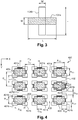
- the figure 3 is a sectional view of the stack taken at the bonding interface and limited to two 3D interconnection pads belonging to chips different.
- the interconnection pad 104a of the upper chip and the interconnection pad 104b of the lower chip have rectangular sections of the same dimensions and are oriented perpendicular to one another.
- the ratio length L over width W of the pads 104a-104b is between 2 and 4.
- the maximum misalignment tolerated, making it possible to obtain a constant contact area, is in each direction equal to ⁇ L / 2, ie a tolerance interval. of length L.
- the 3D interconnection structures described above make the performance of 3D circuits more homogeneous and improve their reliability, but complicates the manufacturing process, in particular the planarization step of the mechanical mechanical polishing bonding surfaces ("Chemical Mechanical Planarization”). , CMP). Indeed, the metal (copper) which constitutes the interconnection pads is not uniformly distributed on the surface of the chips. In the solution proposed by SW. Kim et al., The metal density, which represents the area of the pads on the total bonding surface, is only about 6% (0.9 2 / 3.6 2 ) for the lower chip. Large portions of silicon oxide thus separate the interconnection pads 104b (cf. Fig.2 ).
- the oxide portions are also very important on the chip surface of the document US2017 / 154873 due to the perpendicular orientation of the pads and their position at the periphery of the chips. Since silicon oxide is polished faster than metal, it is difficult to obtain a planar bonding surface with such structures.
- N N necessarily being greater than or equal to 4
- N N necessarily being greater than or equal to 4
- second interconnection pads regularly distributed on the surface of the second chip and interconnected electrically.
- This constant contact surface makes it possible to obtain identical electrical performances regardless of the misalignment value (in the tolerance range) and a uniform bonding energy, within the same plate or between several plates / chips. The quality of the bonding and therefore the reliability of the stack is therefore improved.
- the contact surface between the first stud and the group of second studs may extend over the entire surface of a second stud of the group or may be distributed over several (up to N) second studs of the group.
- the first dimension of the first interconnect pads is equal to the third repetition step
- the second dimension of the first interconnect pads is equal to the fourth repetition step
- the first distance is equal to at the third step of repetition
- the second distance is equal to the fourth step of repetition.
- the first dimension of the first interconnect pads is twice the third repetition step
- the second dimension of the first interconnect pads is twice the fourth repetition step
- the first distance is equal to twice the third step of repetition and the second distance is twice the fourth step of repetition.
- the stack according to the invention may also have one or more of the characteristics below, considered individually or in any technically possible combination.
- the first dimension of the first interconnect pads is further equal to the first repeat pitch divided by 2 and the second dimension of the first interconnect pads is further equal to the second repeat pitch divided by 2.
- the density of metal on the surface of the first chip is then equal to 25%. This configuration corresponds to a homogeneous distribution of the metal in each of the first and second directions.
- the first step of repetition is advantageously equal to the second step of repetition.
- the distribution of the metal surface of the first chip is then the same in the first and second directions.
- the second interconnection pads have for example a rectangular, round or octagonal section.
- the second interconnect pads have a first dimension in the first direction equal to the third repeat pitch divided by 2 and a second dimension in the second direction equal to the fourth repeat pitch divided by 2.
- Surface metal density of the second chip is then equal to 25%. This configuration corresponds to a homogeneous distribution of the metal in each of the first and second directions.
- the third repetition step is advantageously equal to the fourth repetition step.
- the distribution of the metal surface of the second chip is then the same in the first and second directions.
- the second chip comprises a layer of active components and a plurality of metal interconnection levels connecting the components. active, and at least one of the metal interconnection levels serves to interconnect the N second interconnection pads of each group.
- 3D interconnection structure is the set of interconnection pads that electrically connect two electronic chips stacked (vertically) one on the other. These interconnection pads are present on one face of each electronic chip, which may be the front face or the rear face.
- the front face of an electronic chip designates the face of a substrate, generally a semiconductor material such as silicon, on which active components are formed, for example transistors, then (if appropriate) passive components. and levels of metal interconnections.
- the rear face of the electronic chip is the face of the substrate opposite to the front face.
- the two electronic chips are glued together, preferably by a direct bonding technique (ie without introducing an intermediate compound - such as an adhesive, a wax or a low-melting point alloy - at the bonding interface ), for example of the metal-metal type or of the metal-dielectric hybrid type.
- the bonding can be done according to different approaches: front face against front side, rear face against back side or front face against back side.
- the two faces which are glued together are substantially planar, their topology generally not exceeding 15 nm. There is no space between the chips after bonding, unlike other assembly technologies (typically microbeads or micro-pillars), which have an important topology (of the order of a few ⁇ m) and require the introduction of a polymer between the chips.
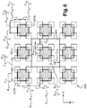
- the figure 4 is a partial sectional view of a stack of electronic chips according to a first embodiment of the invention. This view is taken at a gluing interface between two electronic chips and schematically represents a first 3D interconnect structure 400 providing the electrical connection between the two electronic chips.
- the 3D interconnect structure 400 comprises a plurality of identical first interconnection pads 401a belonging to a first electronic chip and a plurality of second identical interconnection pads 401b belonging to a second electronic chip.
- the face of the first chip, on which the first interconnection pads 401a open, is glued to the face of the second chip showing the second interconnection pads 401b.
- the first interconnection pads 401a and the second interconnection pads 401b are preferably metal, for example copper or aluminum, and participate in bonding the first and second chips.
- the second interconnection pads 401b of the second chip, as well as the first interconnection pads 401a of the first chip, are spaced apart from each other by electrically insulating portions 402, for example made of silicon oxide.
- the bonding surface of each chip is composed of metal interconnection pads surrounded by a dielectric material.
- the first interconnection pads 401a of the first chip are distinct and arranged in rows and columns, in the form of a matrix or mesh.
- the columns of first pads 401a have a first pitch P X1 in a first direction X of the cutting plane of the figure 4 .
- This first repetition step P X1 is equal to the distance separating the centers of two studs 401a belonging to the same line and to two consecutive columns.
- the lines of first pads 401a have a second pitch P Y1 in a second direction Y of the plane, perpendicular to the first direction X.
- This second pitch of repetition P Y1 is equal to the distance that separates the centers two studs 401a belonging to the same column and two consecutive lines.
- the first interconnection pads 401a are reproduced periodically on the surface of the first chip, and in both directions X and Y.
- the second interconnection pads 401b of the second chip are also distinct and arranged in rows and columns.
- the columns of second pads 401b are repeated in the first direction X in a third pitch P X2
- the lines of second pads 401b are repeated in the second direction Y in a fourth pitch P Y2 .
- the third and fourth repetition steps P X2 -P Y2 are defined in the same way as the first and second no repeat P X1 -P Y1 , compared to the centers of the second pads 401b.
- the number of rows and columns, and therefore interconnect pads on the surface of each chip depends on the desired interconnect density and the area of chip bonding surfaces. So as not to unnecessarily figure 4 only three columns and three rows of first pads 401a are shown and only six columns and six rows of second pads 401b are shown.
- the first repeat pitch P X1 (no X repeat of the first pads 401a) may be different from the second repeat pitch P Y1 (no Y repeat of the first pads 401a) and the third repeat pitch P X2 (not X repeat of the second pads 401b) may be different from the fourth repeat pitch P Y2 (no repeat Y of the second pads 401b).
- the first pads 401a and the second pads 402b are then in the form of rectangular meshes.
- the first interconnection pads 401a have a section, in the plane of the bonding face, of rectangular shape.
- the dimensions of the first pads 401a in the first direction X and in the second direction Y are respectively denoted Axi and A Y1 .
- the section of the second interconnection pads 401b (in the plane of the bonding face) may be of any shape, for example rectangular (cf. Fig.4 ), round or octagonal.
- the dimensions of the second pads 401b in the first direction X and in the second direction Y are denoted respectively A X2 and A Y2 .
- the distance separating in the X direction two consecutive second pads 401b belonging to the same line is denoted D X2 and the distance separating in the Y direction two second consecutive pads 401b belonging to the same column is denoted D Y2 .
- the Axis X dimension of the first pads 401a is equal to the third pitch P X2 and the dimension Y1 Y of the first pads 401a is equal to the fourth pitch P Y2 .
- the distance D X1 which separates in the direction X two first consecutive pads 401a of the same line, that is to say, the width of the insulating portion 402 separating two consecutive columns of first pads 401a is equal to the third pitch P X2 .
- the distance D Y1 separating in the Y direction two consecutive first pads 401a of the same column is equal at the fourth repetition step P Y2 .
- the second interconnection pads 401b are interconnected by N group, preferably by means of metal tracks 403 located in a plane parallel to the bonding face of the second chip.
- Each group of second interconnection pads 401b is electrically connected to a single first interconnection pad 401a.
- at least one second pad 401b of each group is in direct contact with the first pad 401a associated with the group.
- the number N of second pads 401b in the groups varies according to the dimensions A X1 -A Y1 of the first pads 401a and spacings D X1 -D Y1 between the first pads 401a.
- the second chip comprises several levels of metal interconnections (belonging to a functional block or set of technological levels called “Back End Of Line” or BEOL) connecting active components (belonging to a functional block called “Front End Of Line” Or FEOL), for example transistors.
- At least one of the metal interconnection levels is advantageously used to interconnect the N second interconnection pads of each group.
- the metal tracks 403 connecting the second pads 401b are added at this level of metal interconnections.
- the metal tracks 403 are added to the last two metal interconnection levels (ie those furthest away from the active components), the interconnection density of which is lower. These last two levels are usually used to realize the power delivery network of the chip and the creation of additional metal tracks 403 does not impact the performance of this grid.
- a particularity of the interconnection structure 400 is that the contact surface S between each first pad 401a and the N second pads 401b of the associated group is independent of the misalignment related to the bonding of the first and second chips, as long as this misalignment does not exceed (in X and Y) threshold values delimiting a tolerance interval (or window).
- the configuration shown on the figure 4 is that of a perfect alignment between the two chips (misalignment in X and Y).
- Each first pad 401a is centered on the group of second pads 401b to which it is connected.
- the contact surface S is distributed uniformly over the four second pads 401b of the group. It is equal to the area of a second stud 401b.
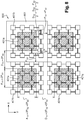
- the Figures 5A and 5B show two other configurations of the interconnection structure 400 (after chip bonding), in which the misalignment between the chips is non-zero.
- the contact surface S is always distributed on the four pads of the group, but more uniformly.
- the contact surface S is nevertheless identical to the configuration of the figure 4 because the sum of the first pad contact surfaces 401a to second pad 401b (so-called individual contact surfaces) is equal to the area of a second pad 401b.
- a constant contact surface also implies identical bonding energy between the different stacks, which is particularly beneficial in the case of plate-and-plate-plate transfer techniques because the stacks must then be cut.
- the reliability of 3D circuits from a mechanical point of view is thus globally improved.
- the figure 6 schematically represents a second 3D interconnection structure 600 belonging to a stack of chips according to a second embodiment of the invention.
- the second interconnect structure 600 represents a particular case of the first interconnect structure 400, since the first and second interconnect pads 401a-401b have a square-shaped section. Consequently, the dimension A X1 at X of the first pads 401a is equal to the dimension A Y1 at Y of the first pads 401a and the dimension A X2 at X of the second pads 401b is equal to the dimension A Y2 at Y of the second pads 401b .
- the X1 dimension at X of the first pads 401a is advantageously equal to the first pitch of repetition P X1 divided by two and the dimension A Y1 in Y of the first pads 401a is advantageously equal to the second pitch of repetition P Y1 divided by two.
- a metal density di of 25% represents an optimal solution for facilitating the preparation of the first chip, and more particularly the chemical-mechanical polishing step of its bonding face, since the metal portions (pads 401a) in X and in Y are of the same width as the dielectric portions (402).
- first repetition step P X1 is equal to the second repetition step P Y1 (the mesh of first studs 401a is therefore itself square).
- the distribution of the metal is then the same in the direction of the lines (X) and in the direction of the columns (Y).
- the dimension A X2 at X of the second pads 401b and the dimension A Y2 at Y of the second pads 401b are respectively equal to the third pitch of repetition P X2 divided by two and at the fourth pitch of repetition P Y2 divided by two.
- the manufacturing advantages described for the first chip are therefore also valid for the second chip.
- the metal density of one of the two chips (the upper chip) in the interconnection structure of the prior art is only about 6%.
- the third repetition step P X2 is equal to the fourth repetition step P Y2 (the mesh of second interconnect pads 401b is therefore also square).
- F X The maximum misalignment allowed in X, denoted hereinafter F X , in the interconnection structure 600 is equal to half the dimension A X2 of the second pads 401b plus the distance D X2 between two second pads 401b consecutive. Indeed, a first pad 401a must not come into contact with the second pads 401b of the adjacent groups.
- the tolerance window represented by area 601 on the figure 6 , thus has a length in X equal to 75% of the first pitch P X1 .
- the maximum misalignment allowed in Y (denoted by F Y ) is identical to that allowed in X (because the distances, dimensions and no repetition in Y are the same as in X), ie a window of tolerance of width in Y equal to 75% of the first repetition step P X1 .
- the interconnection structure 600 according to the invention therefore tolerates greater misalignment than the structure of FIG. interconnection of the prior art.
- the figure 7 schematically represents a third 3D interconnection structure 700 belonging to a stack of chips according to a third embodiment of the invention.
- the third interconnect structure 700 differs from the second interconnect structure 600 only in the form of the second interconnect pads 401b.
- the section of the second studs 401b is indeed not limited to a rectangular shape ( Fig.4 ) or square ( Fig.6 ).
- a constant contact area S (regardless of the misalignment in the tolerance interval) is indeed obtained even if the section of the second pads 401b is not symmetrical in X and Y. In the embodiment of FIG. figure 7 , the contact area S is still equal to the area of a second stud 401b.
- the first and second studs 401a-401b are of square section and organized according to equally square meshes.
- the first pitch P X1 is equal to the second pitch P Y1 and the third pitch P X2 is equal to the fourth pitch P Y2 .
- the dimensions A X2 (in X) and A Y2 (in Y) of the second pads 401b are equal to the third pitch P X2 divided by 2.
- the densities d 1 and d 2 of metal are therefore always equal to 25%.
- the number N of second interconnected pads in each group is equal to 16 (they are distributed according to a 4x4 matrix).
- the contact surface S is constant and equal to the area of four second pads 401b, regardless of the misalignment value in the tolerance range.
- the tolerance window represented by the 801 field on the figure 8 , thus has a length in X and a width in Y equal to 62.5% of the first pitch P X1 .
- N 4
- the interconnection structures 400, 600, 700 and 800 described below tolerate, in addition to a misalignment related to chip bonding (and represented by the Figures 5A-5B ), an offset interconnect pads within a chip.
- the contact surface S between a first pad 401a and a group of second pads 401b remains constant even if the distance between the pads 401a or 401b varies slightly within the matrix.
- This offset is variable depending on the position on the wafer (low between two neighboring studs, but may be important between two distant pads on the wafer). It is for example due to an expansion of materials or misalignments during chip manufacturing steps (especially photolithography steps).
- the electrical performance of the 3D interconnections, and in particular their electrical resistance, are therefore homogeneous within the same stack. For the same reason, the bonding energy is homogeneous within the same stack, which improves the mechanical strength and reliability of the stack.
- interconnection structures are usable regardless of the value of the repetition pitch of the first pads 401a, called no "functional" repetition because it sets the density of the 3D interconnections in the stack.
- they are particularly advantageous for a functional repeat pitch of less than 2 ⁇ m. Indeed, with such a repetition step, the 3D interconnection pads and the metal lines of the upper interconnection levels have very close dimensions. The interest of having a constant contact surface S, and therefore a homogeneous electrical resistance, is therefore very strong.
- the functional repeat pitch is of the order of 4-5 ⁇ m or more, the 3D interconnect pads are larger and the strength of the metal lines is large compared to that of the 3D interconnect pads.
- the variation of the contact surface S thus influences to a lesser extent the overall electrical performance of the interconnections that connect the active components of the two chips (3D interconnects, metallic lines of the interconnection levels and vias between the levels).
- the stack of electronic chips according to the invention comprises at least the first and second electronic chips.
- the first chip provided with the first interconnection pads 401a may be disposed on the second chip provided with the second interconnection pads 401b, or vice versa.
- a stack of more than two electronic chips comprises more than one 3D interconnection structure and at least one of the electronic chips has interconnect pads on its two faces (front face and back face).
Landscapes
- Internal Circuitry In Semiconductor Integrated Circuit Devices (AREA)
- Wire Bonding (AREA)
- Engineering & Computer Science (AREA)
- Manufacturing & Machinery (AREA)
- Physics & Mathematics (AREA)
- Geometry (AREA)
Abstract
Description
- La présente invention est relative aux circuits intégrés en trois dimensions (3D IC) et concerne plus particulièrement un empilement 3D de puces électroniques qui tolère un désalignement important entre deux puces électroniques superposées.
- L'intégration tridimensionnelle (3D) consiste à empiler plusieurs puces électroniques (aussi appelées circuits intégrés) et à les relier électriquement entre elles, par exemple par une technique de collage. Cette approche permet notamment de réduire l'encombrement des systèmes dits « hétérogènes » qui sont composés de circuits appartenant à des technologies différentes, par exemple un capteur d'image comprenant une matrice de photodiodes et un circuit CMOS de traitement d'image comprenant des transistors. L'intégration 3D permet également d'augmenter la densité de transistors par unité de surface sans réduire leurs dimensions et de diminuer la consommation électrique d'un système, en remplaçant de longues interconnexions horizontales par de courtes interconnexions verticales.
- Un circuit 3D peut adopter plusieurs architectures en fonction notamment de la manière dont sont empilées les puces, de l'orientation des puces et du type de collage.
- L'empilement peut être réalisé selon différentes approches : de plaque à plaque (pour « wafer-to-wafer » en anglais), de puce à plaque (« die-to-wafer ») ou encore de puce à puce (« die-to-die »). La technique d'empilement plaque à plaque est la plus rapide en nombre de puces collées par heure, car il s'agit d'un collage collectif à l'échelle des plaques de silicium. Elle est également la plus précise pour une vitesse de collage donnée. Par contre, à la différence des deux autres techniques, elle n'offre pas la possibilité de n'assembler que les puces fonctionnelles (dites « Know Good Dies »), sélectionnées après une série de tests et la découpe des plaques. Le rendement après assemblage obtenu par la technique plaque à plaque est donc inférieur au rendement de la technique puce à plaque et au rendement de la technique puce à puce. Cette dernière technique est naturellement la plus longue à mettre oeuvre, car les puces sont collées entre elles deux par deux après la découpe des plaques.
- Lorsque les puces (ou les plaques) sont orientées dans le même sens, la face avant d'une puce est collée à la face arrière d'une autre puce. Ce mode d'assemblage est appelé « back-to-face ». Inversement, lorsque les puces (ou les plaques) sont assemblées après retournement de l'une d'entre elles, les puces sont collées face avant contre face avant (« face-to-face ») ou face arrière contre face arrière (« back-to-back »).
- La
figure 1 illustre un exemple de circuit 3D intégrant une première puce 100a et une deuxième 100b dans un boîtier (ici BGA) composé d'un substrat 110 et d'un capot 120. La première puce 100a, dite puce supérieure, est empilée sur la deuxième puce 100b, appelée puce inférieure. Chaque puce comprend, de la face arrière BS à la face avant FS, un substrat en silicium 101, un premier bloc fonctionnel 102 (ou ensemble de niveaux technologiques) appelé FEOL (« Front End Of Line ») qui regroupe les composants actifs (ex. transistors) de la puce, et un deuxième bloc fonctionnel 103 appelé BEOL (« Back End Of Line ») qui regroupe les composants passifs (ex. résistances, inductances, capacités) et les interconnexions de la puce. Les interconnexions du bloc BEOL 103 sont typiquement réparties en plusieurs niveaux de métal. - Les puces 100a-100b sont dans cet exemple assemblées face avant contre face avant (« face-to-face ») par une technique de collage direct de type hybride. Chaque puce présente en face avant FS une surface de collage composée de plots d'interconnexion 104 en métal et de portions isolantes 105, typiquement en oxyde de silicium. Les portions isolantes 105 séparent les plots d'interconnexion 104. Les plots d'interconnexion 104 de la première puce 100a sont en contact direct avec les plots d'interconnexion 104 de la deuxième puce 100b, de façon à coupler électriquement les deux puces 100a-100b. Les plots d'interconnexion, typiquement en cuivre, participent au collage des deux puces et acheminent des signaux électriques d'une puce à l'autre. Les plots d'interconnexion 104 en face avant FS de chaque puce sont généralement organisés en lignes et en colonnes, sous la forme d'une matrice ou maille. L'ensemble des plots d'interconnexion 104 appartenant aux deux puces 100a-100b constitue une structure dite d'interconnexion 3D.
- Des vias traversants 106 désignés par l'acronyme TSV de l'anglais « Through Silicon Via » s'étendent en outre à travers la puce inférieure 100b, et plus particulièrement du premier niveau de métal du bloc BEOL jusqu'à la face arrière BS. Ces vias traversants 106 servent à acheminer les signaux électriques depuis la face avant FS de la puce 100b jusqu'à sa face arrière BS. Le substrat 101 de la puce inférieure 100b est aminci spécialement pour permettre la réalisation de ces vias.
- Les signaux sont ensuite répartis (ou redistribués) sur la face arrière BS de la puce inférieure 100b, à l'aide d'une couche de redistribution 107 dite RDL (« redistribution layer »). Le rôle de cette couche RDL 107 est de relier électriquement chacun des TSV 106 à une zone de reprise de contact, à partir de laquelle les signaux sont acheminés vers l'extérieur du boîtier protégeant les puces.
- Une technique d'assemblage connue consiste à adopter la même géométrie pour la matrice de plots d'interconnexion 104 de la première puce 100a et la matrice de plots d'interconnexion 104 de la deuxième puce 100b. Les plots d'interconnexion 104 des puces 100a-100b sont alors de même forme, par exemple de section carrée (dans le plan de la face avant FS), de mêmes dimensions et espacés de la même distance. Avec une telle structure d'interconnexion 3D, le moindre désalignement lors du collage des deux puces se traduit par une diminution de la surface de contact entre les plots d'interconnexion 104. Or une diminution de la surface de contact est préjudiciable pour la qualité de collage, notamment d'un point de vue mécanique, et pour les performances électriques de l'empilement. Comme le désalignement a tendance à varier d'un empilement de puces à l'autre (même lorsque les puces inférieures/supérieures appartiennent à une même plaque, i.e. approche puce-à-plaque ou plaque à plaque), une dispersion liée au désalignement apparaît dans les performances des circuits 3D.
- Le document [« Ultra-fine Pitch 3D Intégration Using Face-to-Face Hybrid Wafer Bonding Combined with a Via-Middle Through-Silicon-Via Process », SW. Kim et al., Electronic Components and Technology Conférence (ECTC), IEEE 66th, 2016] propose une solution pour garantir une surface de contact constante entre les plots d'interconnexion 3D de deux puces empilées l'une sur l'autre. Cette solution, illustrée par la
figure 2 , consiste à adopter des matrices de plots d'interconnexion de géométries différentes. La puce supérieure 100a comprend une pluralité de plots d'interconnexion 104a de section carrée agencés en lignes et en colonnes, avec un pas de répétition (« pitch » en anglais) identique dans les deux directions, par exemple égal à 3,6 µm. Les plots d'interconnexion 104a mesurent alors 0,9 µm de côté, soit ¼ du pas de répétition. La puce inférieure 100b comprend des plots d'interconnexion 104b agencés également selon une maille carrée dont le pas de répétition est égal à 3,6 µm. Les plots d'interconnexion 104b mesurent cependant 2,7 µm de côté, soit ¾ du pas de répétition. - Dans le cas représenté sur la
figure 2 , celui d'un alignement parfait entre les deux puces, chaque plot d'interconnexion 104a de la puce supérieure 100a est positionné au centre d'un plot d'interconnexion 104b de la puce inférieure 100b. La surface de contact entre les plots 104a-104b est égale à la superficie du plus petit plot, 104a. Tant que le plot 104a ne dépasse pas du périmètre du plot 104b, c'est-à-dire tant que le désalignement entre les deux puces n'excède pas 0,9 µm dans la direction des lignes et/ou dans la direction des colonnes, cette surface de contact est en outre constante. Comme indiqué dans le document, une résistance de contact constante limite la dispersion des performances électriques au sein d'un même circuit 3D et entre plusieurs circuits 3D, en particulier en termes de résistance électrique. - La demande de brevet
US2017/154873 décrit un autre empilement de puces électroniques qui tolère un désalignement important et garantit une surface de contact constante dans un certain intervalle de tolérance. Les plots d'interconnexion 3D sont dans cet empilement situés à la périphérie des puces. - La
figure 3 est une vue en coupe de l'empilement prise au niveau de l'interface de collage et limitée à deux plots d'interconnexion 3D appartenant à des puces différentes. Le plot d'interconnexion 104a de la puce supérieure et le plot d'interconnexion 104b de la puce inférieure ont des sections rectangulaires de mêmes dimensions et sont orientés perpendiculairement l'un par rapport à autre. Le rapport longueur L sur largeur W des plots 104a-104b est compris entre 2 et 4. Le désalignement maximum toléré, permettant d'obtenir une surface de contact constante, est dans chaque direction égal à ± L/2, soit un intervalle de tolérance de longueur L. - Les structures d'interconnexion 3D décrites ci-dessus rendent les performances des circuits 3D plus homogènes et améliorent leur fiabilité, mais complexifie la fabrication, en particulier l'étape de planarisation des surfaces de collage par polissage mécano-chimique (« Chemical Mechanical Planarization », CMP). En effet, le métal (cuivre) qui constitue les plots d'interconnexion n'est pas réparti de façon uniforme à la surface des puces. Dans la solution proposée par SW. Kim et al., la densité de métal, qui représente la surface des plots sur la surface totale de collage, n'est que de 6 % environ (0,92/3,62) pour la puce inférieure. De larges portions d'oxyde de silicium séparent donc les plots d'interconnexion 104b (cf.
Fig.2 ). Les portions d'oxyde sont également très importantes à la surface des puces du documentUS2017/154873 , du fait de l'orientation perpendiculaire des plots et de leur position à la périphérie des puces. Comme l'oxyde de silicium est poli plus rapidement que le métal, il est difficile d'obtenir une surface de collage plane avec de telles structures. - Il existe donc un besoin de prévoir un empilement de puces électroniques qui soit tolérant au désalignement, fiable, facile à réaliser et dont les performances électriques sont identiques quelle que soit la valeur du désalignement dans un intervalle de tolérance.
- Selon l'invention, on tend à satisfaire ce besoin en prévoyant un empilement 3D de puces électroniques comprenant :
- une première puce présentant sur une première face une pluralité de premiers plots d'interconnexion de section rectangulaire, agencés en lignes et en colonnes, les colonnes de premiers plots d'interconnexion présentant un premier pas de répétition dans une première direction et les lignes de premiers plots d'interconnexion présentant un deuxième pas de répétition dans une deuxième direction perpendiculaire à la première direction ;
- une deuxième puce présentant, sur une deuxième face collée à la première face de la première puce, une pluralité de deuxièmes plots d'interconnexion agencés en lignes et en colonnes, les colonnes de deuxièmes plots d'interconnexion présentant un troisième pas de répétition dans la première direction et les lignes de deuxièmes plots d'interconnexion présentant un quatrième pas de répétition dans la deuxième direction, au moins une partie des deuxièmes plots d'interconnexion étant en contact avec les premiers plots d'interconnexion pour coupler électriquement les première et deuxième puces ;
- les premiers plots d'interconnexion présentent une première dimension dans la première direction égale à m fois le troisième pas de répétition, où m est un entier naturel non nul, et une deuxième dimension dans la deuxième direction égale à n fois le quatrième pas de répétition, où n est un entier naturel non nul ;
- les premiers plots d'interconnexion appartenant à une même ligne et à deux colonnes consécutives sont séparés dans la première direction d'une première distance égale à q fois le troisième pas de répétition, où q est un entier naturel non nul ;
- les premiers plots d'interconnexion appartenant à une même colonne et à deux lignes consécutives sont séparés dans la deuxième direction d'une deuxième distance égale à r fois le quatrième pas de répétition, où r est un entier naturel non nul ;
- les deuxièmes plots d'interconnexion sont interconnectés en une pluralité de groupes, chaque groupe comprenant un nombre N de deuxièmes plots d'interconnexion interconnectés tel que :

- Pour chacun des premiers plots d'interconnexion appartenant à la première puce, il est prévu un groupe de N (N étant nécessairement supérieur ou égal à 4) deuxièmes plots d'interconnexion régulièrement répartis à la surface de la deuxième puce et interconnectés électriquement. En multipliant ainsi le nombre de deuxièmes plots associés à chaque premier plot, une meilleure densité de métal peut être obtenue à la surface de la deuxième puce. La préparation de la deuxième puce avant son collage, et notamment l'étape de planarisation de sa surface de collage, s'en trouve facilitée.
- L'agencement des premiers plots et des deuxièmes plots, sous la forme de matrices dont les dimensions sont liées entre elles (dans chaque direction, la dimension et l'espacement des premiers plots sont des multiples du pas de répétition des deuxièmes plots), garantit en outre une surface de contact entre le premier plot et le groupe de deuxièmes plots associé, tant que le désalignement entre les puces est compris dans une plage de désalignement appelée intervalle ou fenêtre de tolérance. Cette surface de contact constante permet d'obtenir des performances électriques identiques quelle que soit la valeur du désalignement (dans l'intervalle de tolérance) et une énergie de collage homogène, au sein d'une même plaque ou entre plusieurs plaques/puces. La qualité du collage et donc la fiabilité de l'empilement est par conséquent améliorée. Suivant le désalignement entre les puces, la surface de contact entre le premier plot et le groupe de deuxièmes plots peut s'étendre à toute la surface d'un deuxième plot du groupe ou peut être répartie sur plusieurs (jusqu'à N) deuxièmes plots du groupe.
- Dans un mode de réalisation préférentiel de l'invention, la première dimension des premiers plots d'interconnexion est égale au troisième pas de répétition, la deuxième dimension des premiers plots d'interconnexion est égale au quatrième pas de répétition, la première distance est égale au troisième pas de répétition et la deuxième distance est égale au quatrième pas de répétition.
- Dans une variante de réalisation, la première dimension des premiers plots d'interconnexion est égale à deux fois le troisième pas de répétition, la deuxième dimension des premiers plots d'interconnexion est égale à deux fois le quatrième pas de répétition, la première distance est égale à deux fois le troisième pas de répétition et la deuxième distance est égale à deux fois le quatrième pas de répétition.
- L'empilement selon l'invention peut également présenter une ou plusieurs des caractéristiques ci-dessous, considérées individuellement ou selon toutes les combinaisons techniquement possibles.
- De préférence, la première dimension des premiers plots d'interconnexion est en outre égale au premier pas de répétition divisé par 2 et la deuxième dimension des premiers plots d'interconnexion est en outre égale au deuxième pas de répétition divisé par 2. La densité de métal en surface de la première puce est alors égale à 25 %. Cette configuration correspond à une répartition homogène du métal dans chacune des première et deuxième directions.
- Le premier pas de répétition est avantageusement égal au deuxième pas de répétition. La répartition du métal en surface de la première puce est alors la même dans les première et deuxième directions.
- Les deuxièmes plots d'interconnexion ont par exemple une section rectangulaire, ronde ou octogonale.
- De préférence, les deuxièmes plots d'interconnexion présentent une première dimension dans la première direction égale au troisième pas de répétition divisé par 2 et une deuxième dimension dans la deuxième direction égale au quatrième pas de répétition divisé par 2. La densité de métal en surface de la deuxième puce est alors égale à 25 %. Cette configuration correspond à une répartition homogène du métal dans chacune des première et deuxième directions.
- Le troisième pas de répétition est avantageusement égal au quatrième pas de répétition. La répartition du métal en surface de la deuxième puce est alors la même dans les première et deuxième directions.
- Selon un développement, la deuxième puce comprend une couche de composants actifs et une pluralité de niveaux d'interconnexions métalliques reliant les composants actifs, et au moins un des niveaux d'interconnexions métalliques sert à interconnecter les N deuxièmes plots d'interconnexion de chaque groupe.
- D'autres caractéristiques et avantages de l'invention ressortiront clairement de la description qui en est donnée ci-dessous, à titre indicatif et nullement limitatif, en référence aux figures annexées, parmi lesquelles :
- la
figure 1 montre un circuit 3D intégrant un premier exemple d'empilement de puces électroniques selon l'art antérieur ; - la
figure 2 représente une structure d'interconnexion 3D employée dans un deuxième exemple d'empilement de puces électroniques selon l'art antérieur ; - la
figure 3 représente une structure d'interconnexion 3D employée dans un troisième exemple d'empilement de puces électroniques selon l'art antérieur ; - la
figure 4 représente une structure d'interconnexion 3D employée dans un empilement de puces électroniques selon un premier mode de réalisation de l'invention ; - les
figures 5A et 5B illustrent la structure d'interconnexion 3D de lafigure 4 dans des situations de désalignement de valeurs différentes ; - la
figure 6 représente une structure d'interconnexion 3D employée dans un empilement de puces électroniques selon un deuxième mode de réalisation de l'invention ; - la
figure 7 représente une structure d'interconnexion 3D employée dans un empilement de puces électroniques selon un troisième mode de réalisation de l'invention ; et - la
figure 8 représente une structure d'interconnexion 3D employée dans un empilement de puces électroniques selon un quatrième mode de réalisation de l'invention. - Pour plus de clarté, les éléments identiques ou similaires sont repérés par des signes de référence identiques sur l'ensemble des figures.
- Dans la description qui suit, on appelle « structure d'interconnexion 3D » l'ensemble des plots d'interconnexion qui permettent de relier électriquement deux puces électroniques empilées (verticalement) l'une sur l'autre. Ces plots d'interconnexion sont présents sur une face de chaque puce électronique, qui peut être la face avant ou la face arrière. La face avant d'une puce électronique désigne la face d'un substrat, généralement en un matériau semi-conducteur tel que le silicium, sur laquelle sont formés des composants actifs, par exemple des transistors, puis (le cas échéant) des composants passifs et des niveaux d'interconnexions métalliques. La face arrière de la puce électronique est la face du substrat opposée à la face avant.
- Les deux puces électroniques sont collées entre elles, de préférence par une technique de collage direct (i.e. sans introduire de composé intermédiaire - tel qu'un adhésif, une cire ou un alliage à faible point de fusion - au niveau de l'interface de collage), par exemple de type métal-métal ou de type hybride métal-diélectrique. Le collage peut être réalisé selon différentes approches : face avant contre face avant, face arrière contre face arrière ou face avant contre face arrière. Les deux faces qui sont collées entre elles sont sensiblement planes, leur topologie ne dépassant généralement pas 15 nm. Il n'existe alors aucun espace entre les puces après leur collage, à la différence d'autres technologies d'assemblage (typiquement par microbilles ou micro-piliers), qui présentent une topologie importante (de l'ordre de quelques µm) et nécessitent l'introduction d'un polymère entre les puces.
- La
figure 4 est une vue en coupe partielle d'un empilement de puces électroniques selon un premier mode de réalisation de l'invention. Cette vue est prise au niveau d'une interface de collage entre deux puces électroniques et représente schématiquement une première structure d'interconnexion 3D 400 assurant la connexion électrique entre les deux puces électroniques. - La structure d'interconnexion 3D 400 comprend une pluralité de premiers plots d'interconnexion 401 a identiques appartenant à une première puce électronique et une pluralité de deuxièmes plots d'interconnexion 401b identiques appartenant à une deuxième puce électronique. La face de la première puce, sur laquelle débouchent les premiers plots d'interconnexion 401a, est collée à la face de la deuxième puce faisant apparaître les deuxièmes plots d'interconnexion 401b. Les premiers plots d'interconnexion 401a et les deuxièmes plots d'interconnexion 401b sont de préférence en métal, par exemple en cuivre ou en aluminium, et participent au collage des première et deuxième puces.
- Les deuxièmes plots d'interconnexion 401b de la deuxième puce, de même que les premiers plots d'interconnexion 401a de la première puce, sont espacés les uns des autres par des portions 402 isolantes électriquement, par exemple en oxyde de silicium. La surface de collage de chaque puce est donc composée de plots d'interconnexion métalliques entourés d'un matériau diélectrique.
- Les premiers plots d'interconnexion 401 a de la première puce sont distincts et agencés en lignes et en colonnes, sous la forme d'une matrice ou maille. Les colonnes de premiers plots 401a présentent un premier pas de répétition PX1 dans une première direction X du plan de coupe de la
figure 4 . Ce premier pas de répétition PX1 est égal à la distance qui sépare les centres de deux plots 401a appartenant à une même ligne et à deux colonnes consécutives. De la même façon, les lignes de premiers plots 401a présentent un deuxième pas de répétition PY1 dans une deuxième direction Y du plan, perpendiculaire à la première direction X. Ce deuxième pas de répétition PY1 est égal à la distance qui sépare les centres de deux plots 401a appartenant à une même colonne et à deux lignes consécutives. En d'autres termes, les premiers plots d'interconnexion 401a sont reproduits de façon périodique à la surface de la première puce, et ce dans les deux directions X et Y. - Les deuxièmes plots d'interconnexion 401b de la deuxième puce sont également distincts et agencés en lignes et en colonnes. Les colonnes de deuxièmes plots 401b se répètent dans la première direction X selon un troisième pas de répétition PX2, tandis que les lignes de deuxièmes plots 401b se répètent dans la deuxième direction Y selon un quatrième pas de répétition PY2. Les troisième et quatrième pas de répétition PX2-PY2 sont définis de la même manière que les premier et deuxième pas de répétition PX1-PY1, par rapport aux centres des deuxièmes plots 401b.
- Le nombre de lignes et de colonnes, et donc de plots d'interconnexion à la surface de chaque puce, dépend de la densité d'interconnexion recherchée et de la superficie des surfaces de collage des puces. Pour ne pas alourdir inutilement la
figure 4 , seules trois colonnes et trois lignes de premiers plots 401a sont représentées et seules six colonnes et six lignes de deuxièmes plots 401b sont représentées. - Comme illustré sur la
figure 4 , le premier pas de répétition PX1 (pas de répétition en X des premiers plots 401a) peut être différent du deuxième pas de répétition PY1 (pas de répétition en Y des premiers plots 401a) et le troisième pas de répétition PX2 (pas de répétition en X des deuxièmes plots 401b) peut être différent du quatrième pas de répétition PY2 (pas de répétition en Y des deuxièmes plots 401b). Les premiers plots 401a et les deuxièmes plots 402b se présentent alors sous la forme de mailles rectangulaires. - Les premiers plots d'interconnexion 401a ont une section, dans le plan de la face de collage, de forme rectangulaire. Les dimensions des premiers plots 401a dans la première direction X et dans la deuxième direction Y sont notées respectivement Axi et AY1.
- La section des deuxièmes plots d'interconnexion 401 b (dans le plan de la face de collage) peut être de forme quelconque, par exemple rectangulaire (cf.
Fig.4 ), ronde ou octogonale. Les dimensions des deuxièmes plots 401b dans la premier direction X et dans la deuxième direction Y sont notées respectivement AX2 et AY2. La distance qui sépare dans la direction X deux deuxièmes plots 401b consécutifs appartenant à une même ligne est notée DX2 et la distance qui sépare dans la direction Y deux deuxièmes plots 401b consécutifs appartenant à une même colonne est notée DY2. - Dans ce premier mode de réalisation, la dimension Axi en X des premiers plots 401a est égale au troisième pas de répétition PX2 et la dimension AY1 en Y des premiers plots 401a est égale au quatrième pas de répétition PY2. En outre, la distance DX1 qui sépare dans la direction X deux premiers plots 401a consécutifs d'une même ligne, c'est-à-dire la largeur de la portion isolante 402 séparant deux colonnes consécutives de premiers plots 401a, est égale au troisième pas de répétition PX2. De façon similaire, la distance DY1 qui sépare dans la direction Y deux premiers plots 401a consécutifs d'une même colonne, c'est-à-dire la largeur de la portion isolante 402 séparant deux lignes consécutives de premiers plots 401a, est égale au quatrième pas de répétition PY2.
- Bien que séparés physiquement, les deuxièmes plots d'interconnexion 401b sont interconnectés par groupe de N, de préférence au moyen de pistes métalliques 403 situées dans un plan parallèle à la face de collage de la deuxième puce. Chaque groupe de deuxièmes plots d'interconnexion 401b est relié électriquement à un unique premier plot d'interconnexion 401a. Pour réaliser cette connexion électrique, au moins un deuxième plot 401b de chaque groupe est en contact direct avec le premier plot 401a associé au groupe. Le nombre N de deuxièmes plots 401b dans les groupes varie en fonction des dimensions AX1-AY1 des premiers plots 401a et des espacements DX1-DY1 entre les premiers plots 401a. À titre d'exemple, dans le mode de réalisation de la
figure 4 , chaque premier plot 401a est relié à quatre deuxièmes plots 401b interconnectés (N=4). - De préférence, la deuxième puce comprend plusieurs niveaux d'interconnexions métalliques (appartenant à un bloc fonctionnel ou ensemble de niveaux technologiques appelé « Back End Of Line » ou BEOL) reliant des composants actifs (appartenant à un bloc fonctionnel appelé « Front End Of Line » ou FEOL), par exemple des transistors. Au moins un des niveaux d'interconnexions métalliques est avantageusement utilisé pour interconnecter les N deuxièmes plots d'interconnexion de chaque groupe. Autrement dit, les pistes métalliques 403 reliant les deuxièmes plots 401b sont ajoutées à ce niveau d'interconnexions métalliques. Avantageusement, les pistes métalliques 403 sont ajoutées aux deux derniers niveaux d'interconnexions métalliques (i.e. les plus éloignés des composants actifs), dont la densité d'interconnexions est plus faible. Ces deux derniers niveaux sont habituellement utilisés pour réaliser la grille d'alimentation (« Power Delivery Network ») de la puce et la création de pistes métalliques supplémentaires 403 n'impacte pas les performances de cette grille.
- Une particularité de la structure d'interconnexion 400 est que la surface de contact S entre chaque premier plot 401a et les N deuxièmes plots 401b du groupe associé est indépendante du désalignement lié au collage des première et deuxième puces, tant que ce désalignement ne dépasse pas (en X et en Y) des valeurs seuil délimitant un intervalle (ou fenêtre) de tolérance.
- La configuration montrée sur la
figure 4 est celle d'un alignement parfait entre les deux puces (désalignement nul en X et en Y). Chaque premier plot 401a est centré sur le groupe de deuxièmes plots 401b auquel il est connecté. La surface de contact S est répartie de manière uniforme sur les quatre deuxièmes plots 401b du groupe. Elle est égale à la superficie d'un deuxième plot 401b. - Les
figures 5A et 5B montrent deux autres configurations de la structure d'interconnexion 400 (après collage des puces), dans lesquelles le désalignement entre les puces est non nul. Dans la configuration de lafigure 5A , celle d'un désalignement modéré en X et en Y, la surface de contact S est répartie toujours sur les quatre plots du groupe, mais plus de façon uniforme. Toutefois, la surface de contact S est néanmoins identique à la configuration de lafigure 4 , car la somme des surfaces de contact de premier plot 401a à deuxième plot 401b (surfaces de contact dites individuelles) est égale à la superficie d'un deuxième plot 401b. Dans la configuration de lafigure 5B , celle d'un désalignement extrême en X et en Y (en limite des intervalles de tolérance), le contact entre le premier plot 401a et le groupe de deuxièmes plots 401b ne se limite plus qu'à un seul deuxième plot 401b, sur toute sa superficie. La surface de contact S est donc toujours la même. - Cette surface de contact constante, quelle que soit la valeur du désalignement (dans l'intervalle de tolérance) entre les deux puces, permet d'homogénéiser les performances électriques d'un empilement 3D à l'autre, notamment leur résistance électrique. Ceci est valable quelle que soit la technique de report employée : puce à puce, puce à plaque ou plaque à plaque (le désalignement entre les puces peut varier d'un endroit à l'autre des plaques, notamment entre le centre et le bord des plaques).
- Une surface de contact constante implique également une énergie de collage identique entre les différents empilements, ce qui est particulièrement bénéfique dans le cas des techniques de report puce à plaque et plaque à plaque car il faut ensuite procéder au découpage des empilements. La fiabilité des circuits 3D d'un point de vue mécanique est donc globalement améliorée.
- Enfin, on constate que la répartition du métal à la surface de la deuxième puce (deuxièmes plots d'interconnexion 401b) est bien meilleure dans la structure d'interconnexion 400 que celle obtenue (pour la puce supérieure) dans la structure d'interconnexion de l'art antérieur (cf.
Fig.2 , plots d'interconnexion 104a). Ceci est dû au fait chaque premier plot 401a est associé dans la structure d'interconnexion 400 à une multitude (au moins 4) de deuxièmes plots 401b, au lieu d'un seul dans l'art antérieur. Grâce à cette meilleure répartition du métal, la fabrication de la deuxième puce (avant collage) est facilitée, en particulier l'étape d'aplanissement de sa face de collage par polissage mécano-chimique. - La
figure 6 représente schématiquement une deuxième structure d'interconnexion 3D 600 appartenant à un empilement de puces selon un deuxième mode de réalisation de l'invention. - La deuxième structure d'interconnexion 600 représente un cas particulier de la première structure d'interconnexion 400, car les premiers et deuxièmes plots d'interconnexion 401a-401b ont une section de forme carrée. Par conséquent, la dimension AX1 en X des premiers plots 401a est égale à la dimension AY1 en Y des premiers plots 401a et la dimension AX2 en X des deuxièmes plots 401b est égale à la dimension AY2 en Y des deuxièmes plots 401b.
- Comme dans la structure 400 de la
figure 4 , la dimension AX1 en X des premiers plots 401a est avantageusement égale au premier pas de répétition PX1 divisé par deux et la dimension AY1 en Y des premiers plots 401a est avantageusement égale au deuxième pas de répétition PY1 divisé par deux. La densité de métal di de la première puce, qui représente la surface des premiers plots 401a sur la surface totale de collage, est alors égale à 25 % :
- Il découle de ces considérations géométriques que le premier pas de répétition PX1 est égal au deuxième pas de répétition PY1 (la maille de premiers plots 401a est donc elle-même carrée). La répartition du métal est alors la même dans la direction des lignes (X) et dans la direction des colonnes (Y).
- De la même façon avantageuse, la dimension AX2 en X des deuxièmes plots 401b et la dimension AY2 en Y des deuxièmes plots 401b sont égales respectivement au troisième pas de répétition PX2 divisé par deux et au quatrième pas de répétition PY2 divisé par deux. La densité de métal d2 en surface de la deuxième puce est alors elle aussi égale à 25 % :

- Les avantages en termes de fabrication décrits pour la première puce sont donc également valables pour la deuxième puce. À titre de comparaison, la densité de métal de l'une des deux puces (la puce supérieure) dans la structure d'interconnexion de l'art antérieur (cf.
Fig.2 ) n'est que de 6 % environ. - De par ces choix géométriques, le troisième pas de répétition PX2 est égal au quatrième pas de répétition PY2 (la maille de deuxièmes plots d'interconnexion 401b est donc elle aussi carrée).
- Le désalignement maximum autorisé en X, noté ci-après FX, dans la structure d'interconnexion 600 est égal à la moitié de la dimension AX2 des deuxièmes plots 401b plus la distance DX2 entre deux deuxièmes plots 401b consécutifs. En effet, un premier plot 401a ne doit pas entrer en contact avec les deuxièmes plots 401b des groupes adjacents. Le désalignement maximum autorisé en X est donc ici égal à ¾ du troisième pas de répétition PX2 (car AX2 = DX2 = PX2/2) ou encore 3/8 du premier pas de répétition PX1 (car PX1 = AX1 + DX1 = 2*PX2) :

figure 6 , présente donc une longueur en X égale à 75 % du premier pas de répétition PX1. - Le désalignement maximum autorisé en Y (noté FY) est identique à celui autorisé en X (car les distances, dimensions et pas de répétition en Y sont les mêmes qu'en X), soit une fenêtre de tolérance de largeur en Y égale à 75 % du premier pas de répétition PX1.
- À titre de comparaison, dans la structure d'interconnexion de l'art antérieur (
Fig.2 ), la fenêtre de tolérance n'est que de 50 % du pas de répétition (2*0,9 µm/3,6 µm = 0,5), en X et en Y. - Pour un même (premier) pas de répétition (c'est-à-dire une même densité d'interconnexion 3D « fonctionnelles »), la structure d'interconnexion 600 selon l'invention tolère donc un désalignement plus important que la structure d'interconnexion de l'art antérieur.
- La
figure 7 représente schématiquement une troisième structure d'interconnexion 3D 700 appartenant à un empilement de puces selon un troisième mode de réalisation de l'invention. - La troisième structure d'interconnexion 700 diffère de la deuxième structure d'interconnexion 600 uniquement dans la forme des deuxièmes plots d'interconnexion 401b. La section des deuxièmes plots 401b n'est en effet pas limitée à une forme rectangulaire (
Fig.4 ) ou carrée (Fig.6 ). Une surface de contact S constante (quel que soit le désalignement dans l'intervalle de tolérance) est en effet obtenue même si la section des deuxièmes plots 401b n'est pas symétrique en X et en Y. Dans le mode de réalisation de lafigure 7 , la surface de contact S est encore égale à la superficie d'un deuxième plot 401b. - Dans une quatrième structure d'interconnexion 800 représentée par la
figure 8 , les premiers et deuxièmes plots 401a-401b sont de section carrée et organisés selon des mailles également carrées. Le premier pas de répétition PX1 est donc égal au deuxième pas de répétition PY1 et le troisième pas de répétition PX2 est égal au quatrième pas de répétition PY2. Les dimensions Axi (en X) et AY1 (en Y) des premiers plots 401a, ainsi que les distances DX1 (en X) et DY1 (en Y) qui séparent les premiers plots 401a, sont en outre égales à deux fois le troisième (ou quatrième) pas de répétition PX2 (= PY2). Les dimensions AX2 (en X) et AY2 (en Y) des deuxièmes plots 401b sont égales au troisième pas de répétition PX2 divisé par 2. Les densités d1 et d2 de métal sont par conséquent toujours égale à 25 %. Le nombre N de deuxièmes plots interconnectés dans chaque groupe est égal à 16 (ils sont répartis selon une matrice 4x4). La surface de contact S est constante et égale à la superficie de quatre deuxièmes plots 401b, quelle que soit la valeur du désalignement dans l'intervalle de tolérance. - Les désalignements maximum autorisés en X (FX) et en Y (FY) sont égaux à une fois le troisième pas de répétition PX2 plus la moitié de la distance DX2 entre deux deuxièmes plots 401b consécutifs, soit ici 5/4 du troisième pas de répétition PX2 ou encore 5/16 du premier pas de répétition PX1 (car PX1 = AX1 + DX1 = 4*PX2) :

- La fenêtre de tolérance, représentée par la zone 801 sur la
figure 8 , présente donc une longueur en X et une largeur en Y égale à 62,5 % du premier pas de répétition PX1. La fenêtre de tolérance de la quatrième structure d'interconnexion 800 est donc moins étendue que celle de la deuxième structure d'interconnexion 600 (FX = FY = 75 %) mais toujours plus étendue que la fenêtre de tolérance de la structure d'interconnexion selon l'art antérieur. - De façon plus générale, une surface de contact S constante peut être obtenue avec une structure d'interconnexion de type de la
figure 4 dès lors qu'elle remplit les critères suivants : - la dimension AX1 en X des premiers plots 401a est égale à m fois le troisième pas de répétition PX2, où m est un premier entier naturel non nul ;
- la dimension AY1 en Y des premiers plots 401a est égale à n fois le quatrième pas de répétition PY2, où n est un deuxième entier naturel non nul ;
- la distance DX1 qui sépare dans la direction X deux premiers plots 401a consécutifs (d'une même ligne) est égale à q fois le troisième pas de répétition PX2, où q est un troisième entier naturel non nul ;
- la distance DY1 qui sépare dans la direction Y deux premiers plots 401a consécutifs est égale à r fois le quatrième pas de répétition PY2, où r est un quatrième entier naturel non nul.
- Le nombre N de deuxièmes plots d'interconnexion 401 b interconnectés dans chaque groupe satisfait à l'équation suivante :

- La surface de contact S entre chaque premier plot 401a et les N deuxièmes plots 401b du groupe associé est donnée par la formule suivante :

- Dans le premier mode de réalisation (
Fig.4 ), le deuxième mode de réalisation (Fig.6 ) et le troisième mode de réalisation (Fig.7 ), les entiers naturels m, n, q et r valent tous 1 (AX1 = PX2, AY1 = PY2, DX1 = PX2 et DY1 = PY2). Comme indiqué précédent, le nombre N de deuxièmes plots 401b dans chaque groupe est égal à 4 (N = 4) et la surface de contact S est égale à la superficie Splot d'un deuxième plot d'interconnexion 401b (S = Splot). - Dans le quatrième mode de réalisation (
Fig.8 ), les entiers naturels m, n, q et r valent tous 2 (AX1 = 2*PX2, AY1 = 2*PY2, DX1 = 2*PX2 et DY1 = 2*PY2). Le nombre N de deuxièmes plots 401b dans chaque groupe est égal à 16 (N = 16), la surface de contact S est égale à la superficie de quatre deuxièmes plots 401b (S = 4*Splot). - Les structures d'interconnexion 400, 600, 700 et 800 décrites ci-dessous tolèrent, outre un désalignement lié au collage des puces (et représenté par les
figures 5A-5B ), un décalage des plots d'interconnexion au sein même d'une puce. Autrement dit, la surface de contact S entre un premier plot 401a et un groupe de deuxièmes plots 401b reste constante même si la distance entre les plots 401a ou 401b varie légèrement au sein de la matrice. Ce décalage est variable en fonction de la position sur la plaquette (faible entre deux plots voisins, mais peut être important entre deux plots éloignés sur la plaquette). Il est par exemple dû à une dilatation des matériaux ou à des désalignements lors des étapes de fabrication des puces (étapes de photolithographie notamment). Les performances électriques des interconnexions 3D, et notamment leur résistance électrique, sont donc homogènes au sein d'un même empilement. Pour la même raison, l'énergie de collage est homogène au sein d'un même empilement, ce qui améliore la résistance mécanique et la fiabilité de l'empilement. - Ces structures d'interconnexion sont utilisables quelle que soit la valeur du pas de répétition des premiers plots 401a, appelé pas de répétition « fonctionnel » car il fixe la densité des interconnexions 3D dans l'empilement. Elles s'avèrent cependant particulièrement avantageuses pour un pas de répétition fonctionnel inférieur à 2 µm. En effet, avec un tel pas de répétition, les plots d'interconnexion 3D et les lignes métalliques des niveaux d'interconnexions supérieurs ont des dimensions très proches. L'intérêt d'avoir une surface de contact S constante, et donc une résistante électrique homogène, est donc très fort. À l'inverse, lorsque le pas de répétition fonctionnel est de l'ordre de 4-5 µm ou plus, les plots d'interconnexion 3D sont plus gros et la résistance des lignes métalliques est grande devant celle des plots d'interconnexion 3D. La variation de la surface de contact S influe alors dans une moindre mesure sur les performances électriques globales des interconnexions qui relient les composants actifs des deux puces (interconnexions 3D, lignes métalliques des niveaux d'interconnexions et vias entre les niveaux).
- De nombreuses variantes et modifications de l'empilement de puces électroniques selon l'invention apparaîtront à l'homme du métier. Les caractéristiques des structures d'interconnexion 400, 600, 700 et 800, décrites au travers des
figures 4 ,6 à8 , peuvent être aisément combinées entre elles. Il est notamment possible de combiner les caractéristiques relatives à la forme des deuxièmes plots 401b, aux pas de répétition en X et en Y des plots 401a-401b et aux dimensions des plots 401a-401b par rapport aux pas de répétition, pour définir de nouvelles structures d'interconnexion 3D bénéficiant des mêmes avantages. - L'empilement de puces électroniques selon l'invention comprend au moins les première et deuxième puces électroniques. La première puce munie des premiers plots d'interconnexion 401a peut être disposée sur la deuxième puce munie des deuxièmes plots d'interconnexion 401b, ou inversement. Un empilement de plus de deux puces électroniques comprend plus d'une structure d'interconnexion 3D et au moins une des puces électroniques présente des plots d'interconnexion sur ses deux faces (face avant et face arrière).
Claims (9)
- Empilement 3D de puces électroniques comprenant :- une première puce présentant sur une première face une pluralité de premiers plots d'interconnexion (401a) de section rectangulaire, agencés en lignes et en colonnes, les colonnes de premiers plots d'interconnexion présentant un premier pas de répétition (PX1) dans une première direction (X) et les lignes de premiers plots d'interconnexion présentant un deuxième pas de répétition (PY1) dans une deuxième direction (Y) perpendiculaire à la première direction ;- une deuxième puce présentant, sur une deuxième face collée à la première face de la première puce, une pluralité de deuxièmes plots d'interconnexion (401b) agencés en lignes et en colonnes, les colonnes de deuxièmes plots d'interconnexion présentant un troisième pas de répétition (PX2) dans la première direction (X) et les lignes de deuxièmes plots d'interconnexion présentant un quatrième pas de répétition (PY2) dans la deuxième direction (Y), au moins une partie des deuxièmes plots d'interconnexion (401b) étant en contact avec les premiers plots d'interconnexion (401a) pour coupler électriquement les première et deuxième puces ;caractérisé en ce que :- les premiers plots d'interconnexion (401a) présentent une première dimension (AX1) dans la première direction (X) égale à m fois le troisième pas de répétition (PX2), où m est un entier naturel non nul, et une deuxième dimension (AY1) dans la deuxième direction (Y) égale à n fois le quatrième pas de répétition (PY2), où n est un entier naturel non nul ;- les premiers plots d'interconnexion appartenant à une même ligne et à deux colonnes consécutives sont séparés dans la première direction (X) d'une première distance (DX1) égale à q fois le troisième pas de répétition (PX2), où q est un entier naturel non nul ;- les premiers plots d'interconnexion appartenant à une même colonne et à deux lignes consécutives sont séparés dans la deuxième direction (Y) d'une deuxième distance (DY1) égale à r fois le quatrième pas de répétition (PY2), où r est un entier naturel non nul ;- les deuxièmes plots d'interconnexion (401b) sont interconnectés en une pluralité de groupes, chaque groupe comprenant un nombre N de deuxièmes plots d'interconnexion (401b) interconnectés tel que :

- Empilement selon la revendication 1, dans lequel la première dimension (AX1) des premiers plots d'interconnexion (401a) est en outre égale au premier pas de répétition (PX1) divisé par 2 et dans lequel la deuxième dimension (AY1) des premiers plots d'interconnexion est en outre égale au deuxième pas de répétition (PY1) divisé par 2.
- Empilement selon la revendication 2, dans lequel le premier pas de répétition (PX1) est égal au deuxième pas de répétition (PY1).
- Empilement selon l'une quelconque des revendications 1 à 3, dans lequel les deuxièmes plots d'interconnexion (401b) ont une section rectangulaire, ronde ou octogonale.
- Empilement selon l'une quelconque des revendications 1 à 4, dans lequel les deuxièmes plots d'interconnexion (401b) présentent une première dimension (AX2) dans la première direction (X) égale au troisième pas de répétition (PX2) divisé par 2 et une deuxième dimension (AY2) dans la deuxième direction (Y) égale au quatrième pas de répétition (PY2) divisé par 2.
- Empilement selon la revendication 5, dans lequel le troisième pas de répétition (PX2) est égal au quatrième pas de répétition (PY2).
- Empilement selon l'une quelconque des revendications 1 à 6, dans lequel :- la première dimension (AX1) des premiers plots d'interconnexion (401a) est égale au troisième pas de répétition (PX2) ;- la deuxième dimension (AY1) des premiers plots d'interconnexion est égale au quatrième pas de répétition (PY2) ;- la première distance (DX1) est égale au troisième pas de répétition (PX2) ; et- la deuxième distance (DY1) est égale au quatrième pas de répétition (PY2).
- Empilement selon l'une quelconque des revendications 1 à 6, dans lequel :- la première dimension (AX1) des premiers plots d'interconnexion (401a) est égale à deux fois le troisième pas de répétition (PX2) ;- la deuxième dimension (AY1) des premiers plots d'interconnexion est égale à deux fois le quatrième pas de répétition (PY2) ;- la première distance (DX1) est égale à deux fois le troisième pas de répétition (PX2) ; et- la deuxième distance (DY1) est égale à deux fois le quatrième pas de répétition (PY2).
- Empilement selon l'une quelconque des revendications 1 à 8, dans lequel la deuxième puce comprend une couche de composants actifs et une pluralité de niveaux d'interconnexions métalliques reliant les composants actifs, et dans lequel au moins un des niveaux d'interconnexions métalliques sert à interconnecter les N deuxièmes plots d'interconnexion (401b) de chaque groupe.
Applications Claiming Priority (1)
| Application Number | Priority Date | Filing Date | Title |
|---|---|---|---|
| FR1852110A FR3078823B1 (fr) | 2018-03-12 | 2018-03-12 | Empilement 3d de puces electroniques |
Publications (2)
| Publication Number | Publication Date |
|---|---|
| EP3540769A1 true EP3540769A1 (fr) | 2019-09-18 |
| EP3540769B1 EP3540769B1 (fr) | 2020-12-09 |
Family
ID=62528626
Family Applications (1)
| Application Number | Title | Priority Date | Filing Date |
|---|---|---|---|
| EP19161512.9A Not-in-force EP3540769B1 (fr) | 2018-03-12 | 2019-03-08 | Empilement 3d de puces électroniques |
Country Status (4)
| Country | Link |
|---|---|
| US (1) | US10818639B2 (fr) |
| EP (1) | EP3540769B1 (fr) |
| JP (1) | JP2019161228A (fr) |
| FR (1) | FR3078823B1 (fr) |
Cited By (1)
| Publication number | Priority date | Publication date | Assignee | Title |
|---|---|---|---|---|
| US12550760B2 (en) * | 2022-10-26 | 2026-02-10 | Innolux Corporation | Semiconductor device |
Families Citing this family (7)
| Publication number | Priority date | Publication date | Assignee | Title |
|---|---|---|---|---|
| KR102534734B1 (ko) | 2018-09-03 | 2023-05-19 | 삼성전자 주식회사 | 반도체 패키지 |
| CN110416078A (zh) * | 2019-08-02 | 2019-11-05 | 武汉新芯集成电路制造有限公司 | 光刻工艺的扩张补偿的确定方法、装置及器件的制造方法 |
| US11581281B2 (en) | 2020-06-26 | 2023-02-14 | Taiwan Semiconductor Manufacturing Co., Ltd. | Packaged semiconductor device and method of forming thereof |
| EP4216272A4 (fr) * | 2021-04-28 | 2024-10-16 | Changxin Memory Technologies, Inc. | Structure d'unité graphique et structure de matrice graphique |
| CN113314489B (zh) * | 2021-05-27 | 2023-03-10 | 芯盟科技有限公司 | 半导体结构及半导体结构的形成方法 |
| CN113314490B (zh) * | 2021-05-27 | 2023-04-07 | 芯盟科技有限公司 | 半导体结构及半导体结构的形成方法 |
| US12532720B2 (en) * | 2022-07-29 | 2026-01-20 | Taiwan Semiconductor Manufacturing Company, Ltd. | Forming openings through carrier substrate of IC package assembly for fault identification |
Citations (5)
| Publication number | Priority date | Publication date | Assignee | Title |
|---|---|---|---|---|
| FR2828334A1 (fr) * | 2001-08-03 | 2003-02-07 | Schlumberger Systems & Service | Procede pour rendre connectable electriquement et mecaniquement un dispositif electrique ayant une face munie de plots de contacts |
| US20080156521A1 (en) * | 2006-12-27 | 2008-07-03 | Kabushiki Kaisha Toshiba | Printed wiring board, printed circuit board, and electronic device |
| US20140252606A1 (en) * | 2011-10-17 | 2014-09-11 | Panasonic Corporation | Integrated circuit, multicore processor apparatus, and method for manufacturing integrated circuit |
| US20150008575A1 (en) * | 2013-07-03 | 2015-01-08 | Taiwan Semiconductor Manufacturing Company Ltd. | Semiconductor device and manufacturing method thereof |
| US20170154873A1 (en) | 2015-11-27 | 2017-06-01 | Samsung Electronics Co., Ltd. | Semiconductor Devices Including Stacked Semiconductor Chips |
Family Cites Families (1)
| Publication number | Priority date | Publication date | Assignee | Title |
|---|---|---|---|---|
| US9343419B2 (en) * | 2012-12-14 | 2016-05-17 | Taiwan Semiconductor Manufacturing Company, Ltd. | Bump structures for semiconductor package |
-
2018
- 2018-03-12 FR FR1852110A patent/FR3078823B1/fr not_active Expired - Fee Related
-
2019
- 2019-03-08 EP EP19161512.9A patent/EP3540769B1/fr not_active Not-in-force
- 2019-03-11 US US16/298,414 patent/US10818639B2/en active Active
- 2019-03-11 JP JP2019043574A patent/JP2019161228A/ja active Pending
Patent Citations (5)
| Publication number | Priority date | Publication date | Assignee | Title |
|---|---|---|---|---|
| FR2828334A1 (fr) * | 2001-08-03 | 2003-02-07 | Schlumberger Systems & Service | Procede pour rendre connectable electriquement et mecaniquement un dispositif electrique ayant une face munie de plots de contacts |
| US20080156521A1 (en) * | 2006-12-27 | 2008-07-03 | Kabushiki Kaisha Toshiba | Printed wiring board, printed circuit board, and electronic device |
| US20140252606A1 (en) * | 2011-10-17 | 2014-09-11 | Panasonic Corporation | Integrated circuit, multicore processor apparatus, and method for manufacturing integrated circuit |
| US20150008575A1 (en) * | 2013-07-03 | 2015-01-08 | Taiwan Semiconductor Manufacturing Company Ltd. | Semiconductor device and manufacturing method thereof |
| US20170154873A1 (en) | 2015-11-27 | 2017-06-01 | Samsung Electronics Co., Ltd. | Semiconductor Devices Including Stacked Semiconductor Chips |
Non-Patent Citations (2)
| Title |
|---|
| JANI IMED ET AL: "Innovative structures to test bonding alignment and characterize high density interconnects in 3D-IC", 2017 15TH IEEE INTERNATIONAL NEW CIRCUITS AND SYSTEMS CONFERENCE (NEWCAS), IEEE, 25 June 2017 (2017-06-25), pages 153 - 156, XP033141924, DOI: 10.1109/NEWCAS.2017.8010128 * |
| SW. KIM ET AL.: "Electronic Components and Technology Conférence (ECTC", 2016, IEEE, article "Ultra-fine Pitch 3D Intégration Using Face-to-Face Hybrid Wafer Bonding Combined with a Via-Middle Through-Silicon-Via Process" |
Cited By (1)
| Publication number | Priority date | Publication date | Assignee | Title |
|---|---|---|---|---|
| US12550760B2 (en) * | 2022-10-26 | 2026-02-10 | Innolux Corporation | Semiconductor device |
Also Published As
| Publication number | Publication date |
|---|---|
| FR3078823A1 (fr) | 2019-09-13 |
| US20190279965A1 (en) | 2019-09-12 |
| JP2019161228A (ja) | 2019-09-19 |
| FR3078823B1 (fr) | 2020-02-21 |
| US10818639B2 (en) | 2020-10-27 |
| EP3540769B1 (fr) | 2020-12-09 |
Similar Documents
| Publication | Publication Date | Title |
|---|---|---|
| EP3540769B1 (fr) | Empilement 3d de puces électroniques | |
| EP3667728B1 (fr) | Procédé de réalisation d'un dispositif à diodes photo-émettrices et/ou photo-réceptrices et avec une grille de collimation auto-alignée | |
| US7955887B2 (en) | Techniques for three-dimensional circuit integration | |
| EP2192612B1 (fr) | Procédé pour empiler et interconnecter des circuits intégrés | |
| US7897428B2 (en) | Three-dimensional integrated circuits and techniques for fabrication thereof | |
| FR3007403A1 (fr) | Procede de realisation d'un dispositif microelectronique mecaniquement autonome | |
| FR2983638A1 (fr) | Procede de formation d'un circuit integre | |
| FR3045869A1 (fr) | Routage ameliore pour structure integree tridimensionnelle | |
| FR3095719A1 (fr) | Procédé de collage moléculaire hybride et circuit électronique pour la mise en oeuvre d'un tel procédé | |
| EP3182450A1 (fr) | Dispositif d'inductance et son procédé de fabrication | |
| EP3109900B1 (fr) | Procede de fabrication d'une pluralite de dipoles en forme d'ilots ayant des electrodes auto-alignees | |
| EP0665594A1 (fr) | Dispositif tridimensionnel de détection de rayonnement et procédé de fabrication de ce dispositif | |
| EP4141915A1 (fr) | Procédé de fabrication d'une puce électronique encapsulée à l'échelle de la puce ainsi que le dispositif correspondant | |
| FR2745973A1 (fr) | Memoire de masse et procede de fabrication de memoire de masse | |
| EP4409634B1 (fr) | Circuit intégré à puces superposées et connexion capacitive | |
| EP2162908B1 (fr) | Procédé de réalisation d'un dispositif électronique reconstitué et dispositif électronique reconstitué correspondant | |
| FR3118286A1 (fr) | Empilement d’au moins trois puces électroniques | |
| EP2040291B1 (fr) | Procédé de collage de puces sur un substrat de contrainte et procédé de mise sous contrainte d'un circuit de lecture semi-conducteur | |
| EP4120332A1 (fr) | Procédé de fabrication de puces électroniques | |
| WO2018077860A1 (fr) | Systeme electronique comportant une puce electronique formant boitier et procede de fabrication | |
| FR3133705A1 (fr) | Dispositif électronique | |
| JP6844877B2 (ja) | 半導体モジュールの製造方法 | |
| FR3167037A1 (fr) | Procédé de fabrication d’interconnexion pour un dispositif électronique | |
| WO2018002368A1 (fr) | Dispositif electronique ayant une banque integree de composants passifs | |
| EP4709136A1 (fr) | Procede de fabrication d'un assemblage 3d |
Legal Events
| Date | Code | Title | Description |
|---|---|---|---|
| PUAI | Public reference made under article 153(3) epc to a published international application that has entered the european phase |
Free format text: ORIGINAL CODE: 0009012 |
|
| STAA | Information on the status of an ep patent application or granted ep patent |
Free format text: STATUS: REQUEST FOR EXAMINATION WAS MADE |
|
| 17P | Request for examination filed |
Effective date: 20190308 |
|
| AK | Designated contracting states |
Kind code of ref document: A1 Designated state(s): AL AT BE BG CH CY CZ DE DK EE ES FI FR GB GR HR HU IE IS IT LI LT LU LV MC MK MT NL NO PL PT RO RS SE SI SK SM TR |
|
| AX | Request for extension of the european patent |
Extension state: BA ME |
|
| RBV | Designated contracting states (corrected) |
Designated state(s): AL AT BE BG CH CY CZ DE DK EE ES FI FR GB GR HR HU IE IS IT LI LT LU LV MC MK MT NL NO PL PT RO RS SE SI SK SM TR |
|
| REG | Reference to a national code |
Ref country code: DE Ref legal event code: R079 Ref document number: 602019001610 Country of ref document: DE Free format text: PREVIOUS MAIN CLASS: H01L0023000000 Ipc: H01L0025065000 |
|
| RIC1 | Information provided on ipc code assigned before grant |
Ipc: H01L 23/485 20060101ALI20200508BHEP Ipc: H01L 23/525 20060101ALI20200508BHEP Ipc: H01L 25/065 20060101AFI20200508BHEP Ipc: H01L 23/528 20060101ALI20200508BHEP |
|
| GRAP | Despatch of communication of intention to grant a patent |
Free format text: ORIGINAL CODE: EPIDOSNIGR1 |
|
| STAA | Information on the status of an ep patent application or granted ep patent |
Free format text: STATUS: GRANT OF PATENT IS INTENDED |
|
| INTG | Intention to grant announced |
Effective date: 20200708 |
|
| GRAS | Grant fee paid |
Free format text: ORIGINAL CODE: EPIDOSNIGR3 |
|
| GRAA | (expected) grant |
Free format text: ORIGINAL CODE: 0009210 |
|
| STAA | Information on the status of an ep patent application or granted ep patent |
Free format text: STATUS: THE PATENT HAS BEEN GRANTED |
|
| AK | Designated contracting states |
Kind code of ref document: B1 Designated state(s): AL AT BE BG CH CY CZ DE DK EE ES FI FR GB GR HR HU IE IS IT LI LT LU LV MC MK MT NL NO PL PT RO RS SE SI SK SM TR |
|
| REG | Reference to a national code |
Ref country code: GB Ref legal event code: FG4D Free format text: NOT ENGLISH |
|
| REG | Reference to a national code |
Ref country code: CH Ref legal event code: EP Ref country code: AT Ref legal event code: REF Ref document number: 1344273 Country of ref document: AT Kind code of ref document: T Effective date: 20201215 |
|
| REG | Reference to a national code |
Ref country code: DE Ref legal event code: R096 Ref document number: 602019001610 Country of ref document: DE |
|
| REG | Reference to a national code |
Ref country code: IE Ref legal event code: FG4D Free format text: LANGUAGE OF EP DOCUMENT: FRENCH |
|
| PG25 | Lapsed in a contracting state [announced via postgrant information from national office to epo] |
Ref country code: GR Free format text: LAPSE BECAUSE OF FAILURE TO SUBMIT A TRANSLATION OF THE DESCRIPTION OR TO PAY THE FEE WITHIN THE PRESCRIBED TIME-LIMIT Effective date: 20210310 Ref country code: NO Free format text: LAPSE BECAUSE OF FAILURE TO SUBMIT A TRANSLATION OF THE DESCRIPTION OR TO PAY THE FEE WITHIN THE PRESCRIBED TIME-LIMIT Effective date: 20210309 Ref country code: RS Free format text: LAPSE BECAUSE OF FAILURE TO SUBMIT A TRANSLATION OF THE DESCRIPTION OR TO PAY THE FEE WITHIN THE PRESCRIBED TIME-LIMIT Effective date: 20201209 Ref country code: FI Free format text: LAPSE BECAUSE OF FAILURE TO SUBMIT A TRANSLATION OF THE DESCRIPTION OR TO PAY THE FEE WITHIN THE PRESCRIBED TIME-LIMIT Effective date: 20201209 |
|
| REG | Reference to a national code |
Ref country code: AT Ref legal event code: MK05 Ref document number: 1344273 Country of ref document: AT Kind code of ref document: T Effective date: 20201209 |
|
| PG25 | Lapsed in a contracting state [announced via postgrant information from national office to epo] |
Ref country code: BG Free format text: LAPSE BECAUSE OF FAILURE TO SUBMIT A TRANSLATION OF THE DESCRIPTION OR TO PAY THE FEE WITHIN THE PRESCRIBED TIME-LIMIT Effective date: 20210309 Ref country code: LV Free format text: LAPSE BECAUSE OF FAILURE TO SUBMIT A TRANSLATION OF THE DESCRIPTION OR TO PAY THE FEE WITHIN THE PRESCRIBED TIME-LIMIT Effective date: 20201209 Ref country code: SE Free format text: LAPSE BECAUSE OF FAILURE TO SUBMIT A TRANSLATION OF THE DESCRIPTION OR TO PAY THE FEE WITHIN THE PRESCRIBED TIME-LIMIT Effective date: 20201209 |
|
| REG | Reference to a national code |
Ref country code: NL Ref legal event code: MP Effective date: 20201209 |
|
| PG25 | Lapsed in a contracting state [announced via postgrant information from national office to epo] |
Ref country code: NL Free format text: LAPSE BECAUSE OF FAILURE TO SUBMIT A TRANSLATION OF THE DESCRIPTION OR TO PAY THE FEE WITHIN THE PRESCRIBED TIME-LIMIT Effective date: 20201209 Ref country code: HR Free format text: LAPSE BECAUSE OF FAILURE TO SUBMIT A TRANSLATION OF THE DESCRIPTION OR TO PAY THE FEE WITHIN THE PRESCRIBED TIME-LIMIT Effective date: 20201209 |
|
| REG | Reference to a national code |
Ref country code: LT Ref legal event code: MG9D |
|
| PG25 | Lapsed in a contracting state [announced via postgrant information from national office to epo] |
Ref country code: CZ Free format text: LAPSE BECAUSE OF FAILURE TO SUBMIT A TRANSLATION OF THE DESCRIPTION OR TO PAY THE FEE WITHIN THE PRESCRIBED TIME-LIMIT Effective date: 20201209 Ref country code: EE Free format text: LAPSE BECAUSE OF FAILURE TO SUBMIT A TRANSLATION OF THE DESCRIPTION OR TO PAY THE FEE WITHIN THE PRESCRIBED TIME-LIMIT Effective date: 20201209 Ref country code: SK Free format text: LAPSE BECAUSE OF FAILURE TO SUBMIT A TRANSLATION OF THE DESCRIPTION OR TO PAY THE FEE WITHIN THE PRESCRIBED TIME-LIMIT Effective date: 20201209 Ref country code: SM Free format text: LAPSE BECAUSE OF FAILURE TO SUBMIT A TRANSLATION OF THE DESCRIPTION OR TO PAY THE FEE WITHIN THE PRESCRIBED TIME-LIMIT Effective date: 20201209 Ref country code: LT Free format text: LAPSE BECAUSE OF FAILURE TO SUBMIT A TRANSLATION OF THE DESCRIPTION OR TO PAY THE FEE WITHIN THE PRESCRIBED TIME-LIMIT Effective date: 20201209 Ref country code: PT Free format text: LAPSE BECAUSE OF FAILURE TO SUBMIT A TRANSLATION OF THE DESCRIPTION OR TO PAY THE FEE WITHIN THE PRESCRIBED TIME-LIMIT Effective date: 20210409 Ref country code: RO Free format text: LAPSE BECAUSE OF FAILURE TO SUBMIT A TRANSLATION OF THE DESCRIPTION OR TO PAY THE FEE WITHIN THE PRESCRIBED TIME-LIMIT Effective date: 20201209 |
|
| PG25 | Lapsed in a contracting state [announced via postgrant information from national office to epo] |
Ref country code: PL Free format text: LAPSE BECAUSE OF FAILURE TO SUBMIT A TRANSLATION OF THE DESCRIPTION OR TO PAY THE FEE WITHIN THE PRESCRIBED TIME-LIMIT Effective date: 20201209 Ref country code: AT Free format text: LAPSE BECAUSE OF FAILURE TO SUBMIT A TRANSLATION OF THE DESCRIPTION OR TO PAY THE FEE WITHIN THE PRESCRIBED TIME-LIMIT Effective date: 20201209 |
|
| REG | Reference to a national code |
Ref country code: DE Ref legal event code: R097 Ref document number: 602019001610 Country of ref document: DE |
|
| PG25 | Lapsed in a contracting state [announced via postgrant information from national office to epo] |
Ref country code: IS Free format text: LAPSE BECAUSE OF FAILURE TO SUBMIT A TRANSLATION OF THE DESCRIPTION OR TO PAY THE FEE WITHIN THE PRESCRIBED TIME-LIMIT Effective date: 20210409 |
|
| PLBE | No opposition filed within time limit |
Free format text: ORIGINAL CODE: 0009261 |
|
| STAA | Information on the status of an ep patent application or granted ep patent |
Free format text: STATUS: NO OPPOSITION FILED WITHIN TIME LIMIT |
|
| PG25 | Lapsed in a contracting state [announced via postgrant information from national office to epo] |
Ref country code: AL Free format text: LAPSE BECAUSE OF FAILURE TO SUBMIT A TRANSLATION OF THE DESCRIPTION OR TO PAY THE FEE WITHIN THE PRESCRIBED TIME-LIMIT Effective date: 20201209 Ref country code: IT Free format text: LAPSE BECAUSE OF FAILURE TO SUBMIT A TRANSLATION OF THE DESCRIPTION OR TO PAY THE FEE WITHIN THE PRESCRIBED TIME-LIMIT Effective date: 20201209 Ref country code: MC Free format text: LAPSE BECAUSE OF FAILURE TO SUBMIT A TRANSLATION OF THE DESCRIPTION OR TO PAY THE FEE WITHIN THE PRESCRIBED TIME-LIMIT Effective date: 20201209 |
|
| 26N | No opposition filed |
Effective date: 20210910 |
|
| PG25 | Lapsed in a contracting state [announced via postgrant information from national office to epo] |
Ref country code: DK Free format text: LAPSE BECAUSE OF FAILURE TO SUBMIT A TRANSLATION OF THE DESCRIPTION OR TO PAY THE FEE WITHIN THE PRESCRIBED TIME-LIMIT Effective date: 20201209 Ref country code: SI Free format text: LAPSE BECAUSE OF FAILURE TO SUBMIT A TRANSLATION OF THE DESCRIPTION OR TO PAY THE FEE WITHIN THE PRESCRIBED TIME-LIMIT Effective date: 20201209 |
|
| REG | Reference to a national code |
Ref country code: BE Ref legal event code: MM Effective date: 20210331 |
|
| PG25 | Lapsed in a contracting state [announced via postgrant information from national office to epo] |
Ref country code: IE Free format text: LAPSE BECAUSE OF NON-PAYMENT OF DUE FEES Effective date: 20210308 Ref country code: LU Free format text: LAPSE BECAUSE OF NON-PAYMENT OF DUE FEES Effective date: 20210308 Ref country code: ES Free format text: LAPSE BECAUSE OF FAILURE TO SUBMIT A TRANSLATION OF THE DESCRIPTION OR TO PAY THE FEE WITHIN THE PRESCRIBED TIME-LIMIT Effective date: 20201209 |
|
| PGFP | Annual fee paid to national office [announced via postgrant information from national office to epo] |
Ref country code: DE Payment date: 20220322 Year of fee payment: 4 |
|
| PG25 | Lapsed in a contracting state [announced via postgrant information from national office to epo] |
Ref country code: IS Free format text: LAPSE BECAUSE OF FAILURE TO SUBMIT A TRANSLATION OF THE DESCRIPTION OR TO PAY THE FEE WITHIN THE PRESCRIBED TIME-LIMIT Effective date: 20210409 |
|
| PGFP | Annual fee paid to national office [announced via postgrant information from national office to epo] |
Ref country code: FR Payment date: 20220328 Year of fee payment: 4 |
|
| PG25 | Lapsed in a contracting state [announced via postgrant information from national office to epo] |
Ref country code: BE Free format text: LAPSE BECAUSE OF NON-PAYMENT OF DUE FEES Effective date: 20210331 |
|
| REG | Reference to a national code |
Ref country code: CH Ref legal event code: PL |
|
| PG25 | Lapsed in a contracting state [announced via postgrant information from national office to epo] |
Ref country code: LI Free format text: LAPSE BECAUSE OF NON-PAYMENT OF DUE FEES Effective date: 20220331 Ref country code: CH Free format text: LAPSE BECAUSE OF NON-PAYMENT OF DUE FEES Effective date: 20220331 |
|
| PG25 | Lapsed in a contracting state [announced via postgrant information from national office to epo] |
Ref country code: CY Free format text: LAPSE BECAUSE OF FAILURE TO SUBMIT A TRANSLATION OF THE DESCRIPTION OR TO PAY THE FEE WITHIN THE PRESCRIBED TIME-LIMIT Effective date: 20201209 |
|
| PG25 | Lapsed in a contracting state [announced via postgrant information from national office to epo] |
Ref country code: HU Free format text: LAPSE BECAUSE OF FAILURE TO SUBMIT A TRANSLATION OF THE DESCRIPTION OR TO PAY THE FEE WITHIN THE PRESCRIBED TIME-LIMIT; INVALID AB INITIO Effective date: 20190308 |
|
| REG | Reference to a national code |
Ref country code: DE Ref legal event code: R119 Ref document number: 602019001610 Country of ref document: DE |
|
| GBPC | Gb: european patent ceased through non-payment of renewal fee |
Effective date: 20230308 |
|
| PG25 | Lapsed in a contracting state [announced via postgrant information from national office to epo] |
Ref country code: GB Free format text: LAPSE BECAUSE OF NON-PAYMENT OF DUE FEES Effective date: 20230308 |
|
| PG25 | Lapsed in a contracting state [announced via postgrant information from national office to epo] |
Ref country code: GB Free format text: LAPSE BECAUSE OF NON-PAYMENT OF DUE FEES Effective date: 20230308 Ref country code: FR Free format text: LAPSE BECAUSE OF NON-PAYMENT OF DUE FEES Effective date: 20230331 Ref country code: DE Free format text: LAPSE BECAUSE OF NON-PAYMENT OF DUE FEES Effective date: 20231003 |
|
| PG25 | Lapsed in a contracting state [announced via postgrant information from national office to epo] |
Ref country code: MK Free format text: LAPSE BECAUSE OF FAILURE TO SUBMIT A TRANSLATION OF THE DESCRIPTION OR TO PAY THE FEE WITHIN THE PRESCRIBED TIME-LIMIT Effective date: 20201209 |
|
| PG25 | Lapsed in a contracting state [announced via postgrant information from national office to epo] |
Ref country code: TR Free format text: LAPSE BECAUSE OF FAILURE TO SUBMIT A TRANSLATION OF THE DESCRIPTION OR TO PAY THE FEE WITHIN THE PRESCRIBED TIME-LIMIT Effective date: 20201209 |
|
| PG25 | Lapsed in a contracting state [announced via postgrant information from national office to epo] |
Ref country code: MT Free format text: LAPSE BECAUSE OF FAILURE TO SUBMIT A TRANSLATION OF THE DESCRIPTION OR TO PAY THE FEE WITHIN THE PRESCRIBED TIME-LIMIT Effective date: 20201209 |