EP3540503A1 - Display screen, display device and mobile terminal - Google Patents
Display screen, display device and mobile terminal Download PDFInfo
- Publication number
- EP3540503A1 EP3540503A1 EP19168690.6A EP19168690A EP3540503A1 EP 3540503 A1 EP3540503 A1 EP 3540503A1 EP 19168690 A EP19168690 A EP 19168690A EP 3540503 A1 EP3540503 A1 EP 3540503A1
- Authority
- EP
- European Patent Office
- Prior art keywords
- light
- light shielding
- layer
- display
- fingerprint module
- Prior art date
- Legal status (The legal status is an assumption and is not a legal conclusion. Google has not performed a legal analysis and makes no representation as to the accuracy of the status listed.)
- Granted
Links
- 239000012780 transparent material Substances 0.000 claims description 23
- 239000000049 pigment Substances 0.000 claims description 11
- 239000006260 foam Substances 0.000 claims description 8
- 230000003287 optical effect Effects 0.000 claims description 7
- 239000008187 granular material Substances 0.000 claims description 4
- 230000000149 penetrating effect Effects 0.000 claims description 2
- 239000010410 layer Substances 0.000 description 126
- 238000002834 transmittance Methods 0.000 description 7
- 239000012790 adhesive layer Substances 0.000 description 6
- 230000000007 visual effect Effects 0.000 description 6
- 230000005540 biological transmission Effects 0.000 description 4
- 238000013461 design Methods 0.000 description 4
- 239000003086 colorant Substances 0.000 description 3
- 238000001514 detection method Methods 0.000 description 3
- 239000006059 cover glass Substances 0.000 description 2
- 230000003247 decreasing effect Effects 0.000 description 2
- 238000011161 development Methods 0.000 description 2
- 239000011521 glass Substances 0.000 description 2
- 230000001788 irregular Effects 0.000 description 2
- 238000004519 manufacturing process Methods 0.000 description 2
- 239000012528 membrane Substances 0.000 description 2
- 238000000034 method Methods 0.000 description 2
- 239000002245 particle Substances 0.000 description 2
- 239000000843 powder Substances 0.000 description 2
- 238000012545 processing Methods 0.000 description 2
- 239000011347 resin Substances 0.000 description 2
- 229920005989 resin Polymers 0.000 description 2
- 239000000758 substrate Substances 0.000 description 2
- 238000013459 approach Methods 0.000 description 1
- 230000015572 biosynthetic process Effects 0.000 description 1
- 239000004568 cement Substances 0.000 description 1
- 239000011248 coating agent Substances 0.000 description 1
- 238000000576 coating method Methods 0.000 description 1
- 238000013016 damping Methods 0.000 description 1
- 238000005516 engineering process Methods 0.000 description 1
- 230000002708 enhancing effect Effects 0.000 description 1
- 238000001704 evaporation Methods 0.000 description 1
- 238000007496 glass forming Methods 0.000 description 1
- 239000000203 mixture Substances 0.000 description 1
- 238000007639 printing Methods 0.000 description 1
- 230000001737 promoting effect Effects 0.000 description 1
- 239000000565 sealant Substances 0.000 description 1
- 230000035945 sensitivity Effects 0.000 description 1
- 238000004528 spin coating Methods 0.000 description 1
Images

Classifications
-
- G—PHYSICS
- G02—OPTICS
- G02F—OPTICAL DEVICES OR ARRANGEMENTS FOR THE CONTROL OF LIGHT BY MODIFICATION OF THE OPTICAL PROPERTIES OF THE MEDIA OF THE ELEMENTS INVOLVED THEREIN; NON-LINEAR OPTICS; FREQUENCY-CHANGING OF LIGHT; OPTICAL LOGIC ELEMENTS; OPTICAL ANALOGUE/DIGITAL CONVERTERS
- G02F1/00—Devices or arrangements for the control of the intensity, colour, phase, polarisation or direction of light arriving from an independent light source, e.g. switching, gating or modulating; Non-linear optics
- G02F1/01—Devices or arrangements for the control of the intensity, colour, phase, polarisation or direction of light arriving from an independent light source, e.g. switching, gating or modulating; Non-linear optics for the control of the intensity, phase, polarisation or colour
- G02F1/13—Devices or arrangements for the control of the intensity, colour, phase, polarisation or direction of light arriving from an independent light source, e.g. switching, gating or modulating; Non-linear optics for the control of the intensity, phase, polarisation or colour based on liquid crystals, e.g. single liquid crystal display cells
- G02F1/133—Constructional arrangements; Operation of liquid crystal cells; Circuit arrangements
- G02F1/1333—Constructional arrangements; Manufacturing methods
- G02F1/13338—Input devices, e.g. touch panels
-
- G—PHYSICS
- G06—COMPUTING; CALCULATING OR COUNTING
- G06F—ELECTRIC DIGITAL DATA PROCESSING
- G06F3/00—Input arrangements for transferring data to be processed into a form capable of being handled by the computer; Output arrangements for transferring data from processing unit to output unit, e.g. interface arrangements
- G06F3/01—Input arrangements or combined input and output arrangements for interaction between user and computer
- G06F3/03—Arrangements for converting the position or the displacement of a member into a coded form
- G06F3/041—Digitisers, e.g. for touch screens or touch pads, characterised by the transducing means
-
- G—PHYSICS
- G06—COMPUTING; CALCULATING OR COUNTING
- G06F—ELECTRIC DIGITAL DATA PROCESSING
- G06F1/00—Details not covered by groups G06F3/00 - G06F13/00 and G06F21/00
- G06F1/16—Constructional details or arrangements
- G06F1/1613—Constructional details or arrangements for portable computers
- G06F1/1633—Constructional details or arrangements of portable computers not specific to the type of enclosures covered by groups G06F1/1615 - G06F1/1626
- G06F1/1637—Details related to the display arrangement, including those related to the mounting of the display in the housing
-
- G—PHYSICS
- G06—COMPUTING; CALCULATING OR COUNTING
- G06F—ELECTRIC DIGITAL DATA PROCESSING
- G06F1/00—Details not covered by groups G06F3/00 - G06F13/00 and G06F21/00
- G06F1/16—Constructional details or arrangements
- G06F1/1613—Constructional details or arrangements for portable computers
- G06F1/1633—Constructional details or arrangements of portable computers not specific to the type of enclosures covered by groups G06F1/1615 - G06F1/1626
- G06F1/1684—Constructional details or arrangements related to integrated I/O peripherals not covered by groups G06F1/1635 - G06F1/1675
-
- G—PHYSICS
- G06—COMPUTING; CALCULATING OR COUNTING
- G06F—ELECTRIC DIGITAL DATA PROCESSING
- G06F3/00—Input arrangements for transferring data to be processed into a form capable of being handled by the computer; Output arrangements for transferring data from processing unit to output unit, e.g. interface arrangements
- G06F3/01—Input arrangements or combined input and output arrangements for interaction between user and computer
- G06F3/03—Arrangements for converting the position or the displacement of a member into a coded form
- G06F3/041—Digitisers, e.g. for touch screens or touch pads, characterised by the transducing means
- G06F3/0412—Digitisers structurally integrated in a display
-
- G—PHYSICS
- G06—COMPUTING; CALCULATING OR COUNTING
- G06F—ELECTRIC DIGITAL DATA PROCESSING
- G06F3/00—Input arrangements for transferring data to be processed into a form capable of being handled by the computer; Output arrangements for transferring data from processing unit to output unit, e.g. interface arrangements
- G06F3/01—Input arrangements or combined input and output arrangements for interaction between user and computer
- G06F3/03—Arrangements for converting the position or the displacement of a member into a coded form
- G06F3/041—Digitisers, e.g. for touch screens or touch pads, characterised by the transducing means
- G06F3/042—Digitisers, e.g. for touch screens or touch pads, characterised by the transducing means by opto-electronic means
- G06F3/0421—Digitisers, e.g. for touch screens or touch pads, characterised by the transducing means by opto-electronic means by interrupting or reflecting a light beam, e.g. optical touch-screen
-
- G—PHYSICS
- G06—COMPUTING; CALCULATING OR COUNTING
- G06V—IMAGE OR VIDEO RECOGNITION OR UNDERSTANDING
- G06V40/00—Recognition of biometric, human-related or animal-related patterns in image or video data
- G06V40/10—Human or animal bodies, e.g. vehicle occupants or pedestrians; Body parts, e.g. hands
- G06V40/12—Fingerprints or palmprints
- G06V40/13—Sensors therefor
- G06V40/1318—Sensors therefor using electro-optical elements or layers, e.g. electroluminescent sensing
-
- G—PHYSICS
- G06—COMPUTING; CALCULATING OR COUNTING
- G06V—IMAGE OR VIDEO RECOGNITION OR UNDERSTANDING
- G06V40/00—Recognition of biometric, human-related or animal-related patterns in image or video data
- G06V40/10—Human or animal bodies, e.g. vehicle occupants or pedestrians; Body parts, e.g. hands
- G06V40/12—Fingerprints or palmprints
- G06V40/13—Sensors therefor
- G06V40/1324—Sensors therefor by using geometrical optics, e.g. using prisms
-
- H—ELECTRICITY
- H10—SEMICONDUCTOR DEVICES; ELECTRIC SOLID-STATE DEVICES NOT OTHERWISE PROVIDED FOR
- H10K—ORGANIC ELECTRIC SOLID-STATE DEVICES
- H10K59/00—Integrated devices, or assemblies of multiple devices, comprising at least one organic light-emitting element covered by group H10K50/00
- H10K59/40—OLEDs integrated with touch screens
-
- H—ELECTRICITY
- H10—SEMICONDUCTOR DEVICES; ELECTRIC SOLID-STATE DEVICES NOT OTHERWISE PROVIDED FOR
- H10K—ORGANIC ELECTRIC SOLID-STATE DEVICES
- H10K59/00—Integrated devices, or assemblies of multiple devices, comprising at least one organic light-emitting element covered by group H10K50/00
- H10K59/60—OLEDs integrated with inorganic light-sensitive elements, e.g. with inorganic solar cells or inorganic photodiodes
- H10K59/65—OLEDs integrated with inorganic image sensors
-
- G—PHYSICS
- G02—OPTICS
- G02F—OPTICAL DEVICES OR ARRANGEMENTS FOR THE CONTROL OF LIGHT BY MODIFICATION OF THE OPTICAL PROPERTIES OF THE MEDIA OF THE ELEMENTS INVOLVED THEREIN; NON-LINEAR OPTICS; FREQUENCY-CHANGING OF LIGHT; OPTICAL LOGIC ELEMENTS; OPTICAL ANALOGUE/DIGITAL CONVERTERS
- G02F1/00—Devices or arrangements for the control of the intensity, colour, phase, polarisation or direction of light arriving from an independent light source, e.g. switching, gating or modulating; Non-linear optics
- G02F1/01—Devices or arrangements for the control of the intensity, colour, phase, polarisation or direction of light arriving from an independent light source, e.g. switching, gating or modulating; Non-linear optics for the control of the intensity, phase, polarisation or colour
- G02F1/13—Devices or arrangements for the control of the intensity, colour, phase, polarisation or direction of light arriving from an independent light source, e.g. switching, gating or modulating; Non-linear optics for the control of the intensity, phase, polarisation or colour based on liquid crystals, e.g. single liquid crystal display cells
- G02F1/133—Constructional arrangements; Operation of liquid crystal cells; Circuit arrangements
- G02F1/1333—Constructional arrangements; Manufacturing methods
- G02F1/1335—Structural association of cells with optical devices, e.g. polarisers or reflectors
- G02F1/133509—Filters, e.g. light shielding masks
- G02F1/133512—Light shielding layers, e.g. black matrix
-
- H—ELECTRICITY
- H01—ELECTRIC ELEMENTS
- H01L—SEMICONDUCTOR DEVICES NOT COVERED BY CLASS H10
- H01L27/00—Devices consisting of a plurality of semiconductor or other solid-state components formed in or on a common substrate
- H01L27/14—Devices consisting of a plurality of semiconductor or other solid-state components formed in or on a common substrate including semiconductor components sensitive to infrared radiation, light, electromagnetic radiation of shorter wavelength or corpuscular radiation and specially adapted either for the conversion of the energy of such radiation into electrical energy or for the control of electrical energy by such radiation
- H01L27/144—Devices controlled by radiation
- H01L27/146—Imager structures
- H01L27/14601—Structural or functional details thereof
- H01L27/1462—Coatings
- H01L27/14623—Optical shielding
-
- H—ELECTRICITY
- H01—ELECTRIC ELEMENTS
- H01L—SEMICONDUCTOR DEVICES NOT COVERED BY CLASS H10
- H01L27/00—Devices consisting of a plurality of semiconductor or other solid-state components formed in or on a common substrate
- H01L27/14—Devices consisting of a plurality of semiconductor or other solid-state components formed in or on a common substrate including semiconductor components sensitive to infrared radiation, light, electromagnetic radiation of shorter wavelength or corpuscular radiation and specially adapted either for the conversion of the energy of such radiation into electrical energy or for the control of electrical energy by such radiation
- H01L27/144—Devices controlled by radiation
- H01L27/146—Imager structures
- H01L27/14678—Contact-type imagers
-
- H—ELECTRICITY
- H10—SEMICONDUCTOR DEVICES; ELECTRIC SOLID-STATE DEVICES NOT OTHERWISE PROVIDED FOR
- H10K—ORGANIC ELECTRIC SOLID-STATE DEVICES
- H10K59/00—Integrated devices, or assemblies of multiple devices, comprising at least one organic light-emitting element covered by group H10K50/00
- H10K59/60—OLEDs integrated with inorganic light-sensitive elements, e.g. with inorganic solar cells or inorganic photodiodes
Definitions
- the present disclosure relates to a field of display technology, and specifically to a display screen, a display device and a mobile terminal.
- the mobile terminals are mostly provided with a fingerprint recognition module used for fingerprint recognition for a user of the mobile terminal, so as to improve the security of the mobile terminal.
- the fingerprint recognition module is disposed out of a display area of a display panel so as to be prevented from hindering the display.
- a display area-to-screen ratio (the ratio of the display area to the whole display screen) is small with such a structure design, which influences the user experience. Therefore, with such a method that the fingerprint module and the display screen are disposed in a superposition manner, the display area-to-screen ratio can be increased.
- the display screen blocks a sensing signal of the fingerprint module, which causes low fingerprint acquisition efficiency of the fingerprint module and reduces the user experience.
- EP3316093A1 discloses an electronic device that includes a cover glass forming an outer surface of the electronic device, a first guide structure disposed below the cover glass and transmitting light polarized in a specified direction, a display panel disposed below the first guide structure and including a plurality of pixels, a second guide structure disposed below the display panel and transmitting light polarized in the specified direction, and a fingerprint sensor disposed below the second guide structure.
- US20080122803 discloses a touch panel which uses at least one infrared source and an array of infrared sensors to detect objects which are in contact with, or close to, the touchable surface of the panel.
- the panel may be operated in both reflective and shadow modes, in arbirary per-pixel combinations which change over time. For example, if the level of ambient infrared is detected and if that level exceeds a threshold, shadow mode is used for detection of touch events over some or all of the display. If the threshold is not exceeded, reflective mode is used to detect touch events.
- the touch panel includes an infrared source and an array of infrared sensors.
- CN106506746A provides a panel, a sensor component and a mobile terminal.
- the panel comprises a cover plate, a first adhesive layer and a second adhesive layer which are arranged at one side of the cover plate, and a receiver through hole, wherein the receiver through hole penetrates the cover plate, the first adhesive layer and the second adhesive layer;
- the second adhesive layer comprises a first transmitting region and a second transmitting region;
- the first adhesive layer covers the first transmitting region and the second transmitting region so that the first transmitting region and the second transmitting region are hidden and invisible from the cover plate appearance;
- a detection light ray emitted from the first transmitting region is emitted from the receiver through hole, and the reflected light ray formed after the reflecting of the external object enters the second transmitting region through the receiver through hole.
- WO2017129126A1 discloses a devices and optical sensor modules for providing on-screen optical sensing of fingerprints by using an under-screen optical sensor module that captures and detects returned light that is emitted by the display screen for displaying images and that is reflected back by the top surface of the screen assembly.
- an objective of the present disclosure is to provide a display screen, a display device and a mobile terminal, so as to improve fingerprint acquisition efficiency of the fingerprint module.
- the present disclosure provides a display screen, including a display layer and a light shielding layer.
- the display layer includes an upper surface and a lower surface opposite to the upper surface, the upper surface is configured to face a user, the light shielding layer is arranged to the lower surface of the display layer, the light shielding layer has a hole to allow a sensing signal of a fingerprint module to pass through.
- the display layer includes an upper covering plate, a touch sensitive layer, an organic luminous layer, and a lower covering plate superposed in sequence.
- the present disclosure provides a display device, including the above-mentioned display screen, and further including a fingerprint module for recognizing fingerprints from a user and a frame.
- the display screen and the fingerprint module are fastened to the frame, and the fingerprint module is disposed at a side of the light shielding layer away from the display layer and located at a position corresponding to the hole.
- the fingerprint module includes a light emitter and a light inductor, and a first light signal emitted by the light emitter and a second light signal received by the light inductor can pass through the hole.
- the present disclosure further provides a mobile terminal, including the above-mentioned display device.
- the display screen provided in embodiments of the present disclosure includes the display layer and the light shielding layer, the light shielding layer is arranged to the lower surface of the display layer, and the light shielding layer has the hole, allowing the fingerprint module to emit and acquire the sensing signal through the hole and the display layer, thus improving the fingerprint acquisition efficiency of the fingerprint module.
- the display device includes the display screen and the fingerprint module disposed below the display screen.
- the display screen includes the display layer and the light shielding layer, the light shielding layer is fastened to the lower surface of the display layer, and the light shielding layer is provided with the hole.
- the fingerprint module is located at a position corresponding to the hole.
- the fingerprint module includes the light emitter and the light inductor, so as to make it convenient for the light signal emitted by the light emitter to be transmitted to the fingerprint through the hole and the display layer, and to be received by the light inductor through the display layer and the hole after being reflected by the fingerprint, thus realizing the fingerprint recognition function.
- the mobile terminal includes the display device.
- the display device includes the display screen and the fingerprint module disposed below the display screen.
- the display screen includes the display layer and the light shielding layer, the light shielding layer is fastened to the lower surface of the display layer, and the light shielding layer is provided with the hole.
- the fingerprint module is located at a position corresponding to the hole.
- the fingerprint module includes the light emitter and the light inductor, so as to make it convenient for the light signal emitted by the light emitter to be transmitted to the fingerprint through the hole and the display layer, and to be received by the light inductor through the display layer and the hole after being reflected by the fingerprint, thus realizing the fingerprint recognition function.
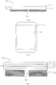
- Fig. 1 illustrates a display screen 100 provided by an embodiment of the present disclosure.
- the display screen 100 includes a display layer 110 and a light shielding layer 120.
- the display layer 110 includes an upper surface 111 and a lower surface 112 opposite to the upper surface, and the upper surface 111 of the display layer 110 is configured to face a user.
- the light shielding layer 120 is fastened to the lower surface 112 of the display layer 110.
- the light shielding layer 120 is affixed to the lower surface 112 of the display layer 110 and configured to block light from penetrating the display layer 110, so as to hide inner structures below the display layer 110 from view and display a color of the light shielding layer 120 when the display layer 110 is in a non-luminous state.
- the light shielding layer 120 has a hole 121 to allow a sensing signal of a fingerprint module to pass through.
- the fingerprint module is an optical fingerprint recognition module
- the hole 121 is configured to allow a light signal emitted and received by the fingerprint module to pass through.
- the display layer 110 mentioned in embodiment of the present application refers to a portion, configured to display an image, of the display screen 100.
- the display screen 100 can also include a non-display layer 113 disposed surrounding the display layer 110.
- the non-display layer 113 is disposed surrounding the display layer 110 and can be used to mount some electronic elements and components that are not disposed in the display layer 110, such as a camera module, an amplifier, or a telephone receiver and the like.
- the display layer 110 mentioned in embodiment of the present application is a light-transparent layer, so as to make it convenient for the fingerprint module to emit and receive the light signal through the display layer 110.
- the light shielding layer 120 is usually disposed below the display layer 110.
- the light shielding layer 120 can be a light-shieling foam layer, or a lightproof ink layer.
- the light shielding layer 120 can hide structures (such as the electronic circuits) below the display screen 100 from view and enables the display layer 110 to present the color of the light shielding layer 120 when the display screen 100 is in the non-luminous state.
- the light shielding layer 120 can be black, white or other colors.
- the display layer 110 includes an upper covering plate 114, a touch sensitive layer 115, an organic luminous layer 116, and a lower covering plate 117 superposed in sequence.
- the light shielding layer 120 can be affixed to the lower covering plate 117.
- the light shielding layer 120 is the lightproof ink layer.
- the hole 121 is disposed in the lightproof ink layer 120, that is, a patterned lightproof ink layer is disposed to the lower covering plate 117, and the patterned lightproof ink layer can be formed on the lower covering plate 117 in a printing, spin coating, coating, or evaporation method.
- the light shielding layer 120 is the foam layer, and the foam layer 120 can play a cushioning and damping role between the lower covering plate 117 and other electronic elements and components.
- the foam layer 120 can be affixed to the lower covering plate 117 by means of a sealant.
- the hole 121 can be processed and formed in the foam layer after the processing of the foam layer is finished, or during the processing of the foam layer.
- the hole 121 can be a circular hole, a square hole, an oval hole or an irregular shaped hole.
- the irregular shaped hole can be a shape adapted to a shape of a contact surface of a fingerprint face contacting with the display screen 100.
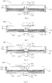
- the display screen 100 further includes a light shielding sheet 130.
- the light shielding sheet 130 is disposed between the display layer 110 and the fingerprint module in the superposition manner and covers the hole 121, so as to hide the fingerprint module and enhance a visual effect of the display screen 100.
- the light shielding sheet 130 covers the hole 121 and is permeable to the light signal, so as to enable the light signal emitted and received by the fingerprint module disposed below the hole 121 to penetrate, and reflect light to hide the fingerprint module.
- reflected light of the light shielding sheet 130 has the same color as reflected light of the light shielding layer 120, so as to make an area of the hole 121 have the same display color as other non-perforated areas of the light shielding layer 120 when the display layer 110 is in a non-display state for example a screen-off state of the mobile terminal, thus reducing visual influence of the hole 121 on the user and enhancing user experience.
- the light shielding sheet 130 includes a light shielding pigment 131 and a light-transparent material 132.
- the light shielding pigment 131 has a similar color to the light shielding layer 120. It could be understood that the color of the light shielding pigment 131 and the color of the light shielding layer 120 are the same when sensed by the user's naked eyes.
- the color of the light shielding layer 120 can be black, white or other colors, and correspondingly, the color of the light shielding pigment 131 can also be black, white or other colors.
- the color of the light shielding pigment 131 is also black, so that the color of the area of the hole 121 and the color of other non-perforated areas of the light shielding layer 120 are consistent, thus reducing the visual influence.
- the light-transparent material 132 forms a light-penetrating passage 133, the light-penetrating passage 133 is along a thickness direction of the display screen 100, and the fingerprint module emits and receives the light signal through the light-penetrating passage 133.
- the light-penetrating passage 133 can increase light transmittance of the light shielding sheet 130.
- the increase of the light transmittance of the light shielding sheet 130 increases transmittance of an incident light emitted from the fingerprint module to the fingerprint, thereby strength of the reflected light from the fingerprint is increased, and transmittance of the reflected light is increased, thus improving accuracy of fingerprint recognition.
- the light-transparent material 132 can be a transparent material such as resin particles, glass powders, or a mixture of resin particles and glass powders. These transparent materials have a certain light transmission property and allow light (arrow part in FIG. 5 ) to pass through.
- the light transmission property of the light shielding sheet 130 can be increased.
- the light-transparent material 132 is formed to be granular. If a granule of the light-transparent material 132 is too small, the light transmission cannot be achieved. If the granule of the light-transparent material 132 is too large, a color difference exists between the light shielding sheet 130 and the light shielding layer 120.
- a size of the granule of the light-transparent material 132 is 1 ⁇ 20 ⁇ m. Further, if a ratio of the light-transparent material 132 to the light shielding sheet 130 is too low, the light transmission property of the light shielding sheet 130 cannot be increased effectively. If the ratio of the light-transparent material 132 to the light shielding sheet 130 is too high, the color of the light shielding sheet 130 will be influenced. Therefore, a mass percent of the light-transparent material 132 to the light shielding sheet 130 is 1% ⁇ 20%.
- the light shielding sheet 130 can be manufactured to be a membrane or a sheet having the light-penetrating passage 133 and then be stuck onto a substrate, and an optical cement can be used for sticking.
- the light-penetrating passage 133 is processed in the membrane or the sheet of the light shielding sheet 130, and thus the display screen 100 is not influenced.
- the light shielding sheet 130 is disposed between the display layer 110 and the light shielding layer 120 in the superposition manner. Specifically, the light shielding sheet 130 can be affixed to the lower covering plate 117 of the display layer 110, or the light shielding sheet 130 can be affixed to an upper surface 122 of the light shielding layer 120.
- the light shielding sheet 130 is disposed between the display layer 110 and the light shielding layer 120, and such a structure design allows the lower covering plate 117 of the display layer 110 to serve as the substrate for affixing of the light shielding sheet 130, thus realizing formation of the light shielding sheet 130 at a lower surface of the lower covering plate 117, which can avoid destroying the structure of the display screen 100 and simplify production process and cost of the light shielding sheet 130.
- the light shielding sheet 130 is fastened to a first surface 123 of the light shielding layer 120, and the first surface 123 is disposed at a side away from the display layer 110.
- the light shielding sheet 130 is disposed at a side of the light shielding layer 120 away from the display layer 110, and with such a structure design, the light shielding layer 120 can be fastened to the display layer 110 and then be affixed to the light shielding sheet 130, that is, the affixation of the light shielding sheet 130 is performed after a position and shape of the hole 121 is determined, which can improve accuracy of covering the hole 121 by the light shielding sheet 130 and reduce technique difficulty of covering the hole 121 by the light shielding sheet 130.
- the light shielding sheet 130 is filled in the hole 121.
- the hole 121 is fully filled with the light shielding sheet 130, that is, a size and shape of the light shielding sheet 130 is consistent with a size and shape of the hole 121, and the light shielding sheet 130 and the light shielding layer 120 are in a common layer and have the same thickness.
- Such a structure design allows the light shielding sheet 130 and the light shielding layer 120 to be in the same layer, so that respective thicknesses of the light shielding sheet 130 and the light shielding layer 120 are decreased significantly and flatness of the light shielding layer 120 is increased on one aspect, hence decreasing the thickness of the display screen 100, and promoting light and thin development of the mobile terminal.
- a display device 200 which includes the display screen 100 according to any one of the above-mentioned embodiments, and further includes a fingerprint module 210 for recognizing fingerprints from a user and a frame 211.
- the display screen 100 and the fingerprint module 210 are fastened to the frame 211.
- the fingerprint module 210 is disposed at a side of the light shielding layer 120 away from the display layer 110 and located at a position corresponding to the hole 121.
- the fingerprint module 210 includes a light emitter 213 and a light inductor 212, and a first light signal emitted by the light emitter 213 and a second light signal received by the light inductor 212 pass through the hole 121.
- the fingerprint module 210 is an optical fingerprint recognition module.
- the light emitter 213 can be a light source such as an LED and the like and be configured to emit incident light to the fingerprint 214.
- the LED light source can be disposed at a position corresponding to the light-penetrating passage 133, the LED source light can also be converted into an area light source by means of a light guide plate so as to increase the transmittance of the incident light in the light shielding sheet 130.
- the light inductor 212 can be a photosensitive sensor for receiving reflected light b formed by the fingerprint 214.
- the light inductor 212 is fastened at a top of the fingerprint module 210, i.e. in a place adjacent to the hole 121.
- the incident light a is cast on the fingerprint 214 through the light inductor 212, the hole 121 and the display layer 110.
- the reflected light b is formed by the reflection of the fingerprint 214, the reflected light b is received by the light inductor 212, and a fingerprint image of fingerprint 214 is obtained after the reflected light b is processed.
- the display screen 100 further includes the light shielding sheet 130.
- the light shielding sheet 130 is disposed between the display layer 110 and the fingerprint module in the superposition manner and covers the hole 121, so as to hide the fingerprint module 210 and enhance the visual effect of the display screen 100.
- the light shielding sheet 130 includes the light shielding pigment 131 and the light-transparent material 132, the light-penetrating passage 133 is formed by the light-transparent material 132, the light-penetrating passage 133 is along the thickness direction of the display screen 100, and the fingerprint module 210 emits or receives the light signal through the light-penetrating passage 133.
- the light-penetrating passage 133 can increase the light transmittance of the light shielding sheet 130.
- the light shielding pigment 131 has a similar color to the light shielding layer 120, thus reducing the visual influence.
- the light emitted by the light emitter 213 forms the incident light a
- the incident light a is cast on the fingerprint 214 through the light inductor 212, the light shielding sheet 130, the hole 121 and the display layer 110 in sequence.
- the light-transparent material 132 can improve the transmittance of the light shielding sheet 130. Therefore, the light shielding sheet 130 has less influence on the incident light a, and the strength of the incident light a cast on the fingerprint 214 is higher.
- the strength of the reflected light b formed by the incident light a being reflected by the fingerprint 214 is also higher.
- the reflected light b formed by the reflection of the fingerprint 214 is cast on the light inductor 212 passing through the display layer 110, the hole 121, and the light shielding sheet 130 in sequence, and is received by the light inductor 212 and forms the fingerprint image.
- the light shielding sheet 130 is disposed between the display screen 100 and the fingerprint module 210 in the superposition manner. Specifically, the light shielding sheet 130 is disposed between a bottom 215 of the frame 211 and the light shielding layer 120 in the superposition manner.
- the light shielding sheet 130 is fastened between the display screen 100 and the fingerprint module 210.
- the fingerprint module 210 includes a second surface 216, the second surface 216 is adjacent to the hole 121, and the light shielding sheet 130 can be affixed to the second surface 216.
- the light shielding sheet 130 is disposed in the hole 121.
- the light shielding sheet 130 can be fully filled in the hole 121, that is, the size and shape of the light shielding sheet 130 are consistent with those of the hole 121, and the light shielding sheet 130 and the light shielding layer 120 are in the same layer and have the same thickness.
- An orthographic projection of the light shielding sheet 130 on the fingerprint module 210 covers the light inductor 212 and the light emitter 213, so as to make it convenient for the incident light emitted by the light emitter 213 to be cast on the fingerprint 214 through the hole 121 and the light shielding sheet 130, and for the light reflected by the fingerprint 214 to be cast on the light inductor 212 through the hole 121 and the light shielding sheet 130.
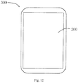
- embodiments of the present disclosure provide a mobile terminal 300, including the display device 200 in any one of the above-mentioned embodiments.
- the display device 200 includes the display screen 100 and the fingerprint module 210 disposed below the display screen 100.
- the display screen 100 includes the display layer 110 and the light shielding layer 120, the light shielding layer 120 is fastened to the lower surface 112 of the display layer 110, and the light shielding layer 120 has the hole 121.
- the fingerprint module 210 is located at the position corresponding to the hole 121.
- the fingerprint module 210 includes the light emitter 213 and the light inductor 212, the light signal emitted by the light emitter 213 is transmitted to the fingerprint 214 through the hole 121 and the display layer 110, and then is received by the light inductor 212 through the display layer 110 and the hole 121 after being reflected by the fingerprint 214, thus improving the fingerprint acquisition and recognition efficiency of the fingerprint module 210.
- the light shielding sheet 130 to cover the hole 121 so as to hide the fingerprint module 210, the visual influence of the hole 121 on the user is reduced and the user experience is enhanced.
Abstract
Description
- The present disclosure relates to a field of display technology, and specifically to a display screen, a display device and a mobile terminal.
- With the rocketing development of the information era, people pay more and more attention to information security issues. The mobile terminals are mostly provided with a fingerprint recognition module used for fingerprint recognition for a user of the mobile terminal, so as to improve the security of the mobile terminal. In the related art, the fingerprint recognition module is disposed out of a display area of a display panel so as to be prevented from hindering the display. A display area-to-screen ratio (the ratio of the display area to the whole display screen) is small with such a structure design, which influences the user experience. Therefore, with such a method that the fingerprint module and the display screen are disposed in a superposition manner, the display area-to-screen ratio can be increased. However, in such a structure, the display screen blocks a sensing signal of the fingerprint module, which causes low fingerprint acquisition efficiency of the fingerprint module and reduces the user experience.
-
EP3316093A1 discloses an electronic device that includes a cover glass forming an outer surface of the electronic device, a first guide structure disposed below the cover glass and transmitting light polarized in a specified direction, a display panel disposed below the first guide structure and including a plurality of pixels, a second guide structure disposed below the display panel and transmitting light polarized in the specified direction, and a fingerprint sensor disposed below the second guide structure. -
US20080122803 discloses a touch panel which uses at least one infrared source and an array of infrared sensors to detect objects which are in contact with, or close to, the touchable surface of the panel. The panel may be operated in both reflective and shadow modes, in arbirary per-pixel combinations which change over time. For example, if the level of ambient infrared is detected and if that level exceeds a threshold, shadow mode is used for detection of touch events over some or all of the display. If the threshold is not exceeded, reflective mode is used to detect touch events. The touch panel includes an infrared source and an array of infrared sensors. -
CN106506746A provides a panel, a sensor component and a mobile terminal. The panel comprises a cover plate, a first adhesive layer and a second adhesive layer which are arranged at one side of the cover plate, and a receiver through hole, wherein the receiver through hole penetrates the cover plate, the first adhesive layer and the second adhesive layer; the second adhesive layer comprises a first transmitting region and a second transmitting region; the first adhesive layer covers the first transmitting region and the second transmitting region so that the first transmitting region and the second transmitting region are hidden and invisible from the cover plate appearance; a detection light ray emitted from the first transmitting region is emitted from the receiver through hole, and the reflected light ray formed after the reflecting of the external object enters the second transmitting region through the receiver through hole. Through the adoption of the panel provided by the invention, the manufacturing process of the mobile terminal can be simplified. Furthermore, the detection sensitivity of an approach sensor is improved, and the condition of misjudgment or failed judgment is effectively avoided. -
WO2017129126A1 discloses a devices and optical sensor modules for providing on-screen optical sensing of fingerprints by using an under-screen optical sensor module that captures and detects returned light that is emitted by the display screen for displaying images and that is reflected back by the top surface of the screen assembly. - Aiming at the above-mentioned problems, an objective of the present disclosure is to provide a display screen, a display device and a mobile terminal, so as to improve fingerprint acquisition efficiency of the fingerprint module.
- In order to solve the existing problems mentioned in the background, the present disclosure provides a display screen, including a display layer and a light shielding layer. The display layer includes an upper surface and a lower surface opposite to the upper surface, the upper surface is configured to face a user, the light shielding layer is arranged to the lower surface of the display layer, the light shielding layer has a hole to allow a sensing signal of a fingerprint module to pass through. The display layer includes an upper covering plate, a touch sensitive layer, an organic luminous layer, and a lower covering plate superposed in sequence.
- The present disclosure provides a display device, including the above-mentioned display screen, and further including a fingerprint module for recognizing fingerprints from a user and a frame. The display screen and the fingerprint module are fastened to the frame, and the fingerprint module is disposed at a side of the light shielding layer away from the display layer and located at a position corresponding to the hole. The fingerprint module includes a light emitter and a light inductor, and a first light signal emitted by the light emitter and a second light signal received by the light inductor can pass through the hole.
- The present disclosure further provides a mobile terminal, including the above-mentioned display device.
- The display screen provided in embodiments of the present disclosure includes the display layer and the light shielding layer, the light shielding layer is arranged to the lower surface of the display layer, and the light shielding layer has the hole, allowing the fingerprint module to emit and acquire the sensing signal through the hole and the display layer, thus improving the fingerprint acquisition efficiency of the fingerprint module.
- The display device provided in embodiments of the present disclosure includes the display screen and the fingerprint module disposed below the display screen. The display screen includes the display layer and the light shielding layer, the light shielding layer is fastened to the lower surface of the display layer, and the light shielding layer is provided with the hole. The fingerprint module is located at a position corresponding to the hole. The fingerprint module includes the light emitter and the light inductor, so as to make it convenient for the light signal emitted by the light emitter to be transmitted to the fingerprint through the hole and the display layer, and to be received by the light inductor through the display layer and the hole after being reflected by the fingerprint, thus realizing the fingerprint recognition function.
- The mobile terminal provided in embodiments of the present disclosure includes the display device. The display device includes the display screen and the fingerprint module disposed below the display screen. The display screen includes the display layer and the light shielding layer, the light shielding layer is fastened to the lower surface of the display layer, and the light shielding layer is provided with the hole. The fingerprint module is located at a position corresponding to the hole. The fingerprint module includes the light emitter and the light inductor, so as to make it convenient for the light signal emitted by the light emitter to be transmitted to the fingerprint through the hole and the display layer, and to be received by the light inductor through the display layer and the hole after being reflected by the fingerprint, thus realizing the fingerprint recognition function.
- To describe the technical solutions in the embodiments of the present disclosure more clearly, the accompanying drawings required for describing the embodiments are briefly introduced in the following. Apparently, the accompanying drawings in the following description show merely some embodiments of the present disclosure, those ordinarily skilled in the art can also derive other drawings from these accompanying drawings without creative efforts.
-
Fig. 1 is a sectional schematic view of a display screen provided in an embodiment of the present disclosure. -
Fig. 2 is a top view of a display screen provided in an embodiment of the present disclosure. -
Fig. 3 is a sectional schematic view of a display screen provided in an embodiment of the present disclosure. -
Fig. 4 is a schematic view of a display screen provided in a first embodiment of the present disclosure. -
Fig. 5 is a sectional schematic view of a light shielding sheet provided in an embodiment of the present disclosure. -
Fig. 6 is a schematic view of a display screen provided in a second embodiment of the present disclosure. -
Fig. 7 is a schematic view of a display screen provided in a third embodiment of the present disclosure. -
Fig. 8 is a sectional schematic view of a display device provided in an embodiment of the present disclosure. -
Fig. 9 is a schematic view of a display device provided in a first embodiment of the present disclosure. -
Fig. 10 is a schematic view of a display device provided in a second embodiment of the present disclosure. -
Fig. 11 is a schematic view of a display device provided in a third embodiment of the present disclosure. -
Fig. 12 is a schematic view of a mobile terminal provided in an embodiment of the present disclosure. - The technical solutions of the embodiments of the present disclosure are clearly and completely described below with reference to the accompanying drawings in the embodiments of the present disclosure.
- Referring to
Fig. 1, Fig. 1 illustrates adisplay screen 100 provided by an embodiment of the present disclosure. Thedisplay screen 100 includes adisplay layer 110 and alight shielding layer 120. Thedisplay layer 110 includes anupper surface 111 and alower surface 112 opposite to the upper surface, and theupper surface 111 of thedisplay layer 110 is configured to face a user. Thelight shielding layer 120 is fastened to thelower surface 112 of thedisplay layer 110. In an embodiment, thelight shielding layer 120 is affixed to thelower surface 112 of thedisplay layer 110 and configured to block light from penetrating thedisplay layer 110, so as to hide inner structures below thedisplay layer 110 from view and display a color of thelight shielding layer 120 when thedisplay layer 110 is in a non-luminous state. Thelight shielding layer 120 has ahole 121 to allow a sensing signal of a fingerprint module to pass through. In the present embodiment, the fingerprint module is an optical fingerprint recognition module, and thehole 121 is configured to allow a light signal emitted and received by the fingerprint module to pass through. - Referring to
Fig. 2 , thedisplay layer 110 mentioned in embodiment of the present application refers to a portion, configured to display an image, of thedisplay screen 100. Thedisplay screen 100 can also include anon-display layer 113 disposed surrounding thedisplay layer 110. Thenon-display layer 113 is disposed surrounding thedisplay layer 110 and can be used to mount some electronic elements and components that are not disposed in thedisplay layer 110, such as a camera module, an amplifier, or a telephone receiver and the like. - It could be understood that the
display layer 110 mentioned in embodiment of the present application is a light-transparent layer, so as to make it convenient for the fingerprint module to emit and receive the light signal through thedisplay layer 110. As thedisplay layer 110 is the light-transparent layer, in order to prevent structures below the display screen 100 (such as the electronic circuits) from being seen, thelight shielding layer 120 is usually disposed below thedisplay layer 110. Thelight shielding layer 120 can be a light-shieling foam layer, or a lightproof ink layer. Thelight shielding layer 120 can hide structures (such as the electronic circuits) below thedisplay screen 100 from view and enables thedisplay layer 110 to present the color of thelight shielding layer 120 when thedisplay screen 100 is in the non-luminous state. Thelight shielding layer 120 can be black, white or other colors. - Referring to
Fig. 3 , thedisplay layer 110 includes anupper covering plate 114, a touchsensitive layer 115, an organicluminous layer 116, and alower covering plate 117 superposed in sequence. Thelight shielding layer 120 can be affixed to thelower covering plate 117. In an embodiment, thelight shielding layer 120 is the lightproof ink layer. Thehole 121 is disposed in thelightproof ink layer 120, that is, a patterned lightproof ink layer is disposed to thelower covering plate 117, and the patterned lightproof ink layer can be formed on thelower covering plate 117 in a printing, spin coating, coating, or evaporation method. In another embodiment, thelight shielding layer 120 is the foam layer, and thefoam layer 120 can play a cushioning and damping role between thelower covering plate 117 and other electronic elements and components. Thefoam layer 120 can be affixed to thelower covering plate 117 by means of a sealant. Thehole 121 can be processed and formed in the foam layer after the processing of the foam layer is finished, or during the processing of the foam layer. - Further, the
hole 121 can be a circular hole, a square hole, an oval hole or an irregular shaped hole. The irregular shaped hole can be a shape adapted to a shape of a contact surface of a fingerprint face contacting with thedisplay screen 100. - Further, referring to
Fig. 4 , thedisplay screen 100 further includes alight shielding sheet 130. Thelight shielding sheet 130 is disposed between thedisplay layer 110 and the fingerprint module in the superposition manner and covers thehole 121, so as to hide the fingerprint module and enhance a visual effect of thedisplay screen 100. Specifically, thelight shielding sheet 130 covers thehole 121 and is permeable to the light signal, so as to enable the light signal emitted and received by the fingerprint module disposed below thehole 121 to penetrate, and reflect light to hide the fingerprint module. Preferably, reflected light of thelight shielding sheet 130 has the same color as reflected light of thelight shielding layer 120, so as to make an area of thehole 121 have the same display color as other non-perforated areas of thelight shielding layer 120 when thedisplay layer 110 is in a non-display state for example a screen-off state of the mobile terminal, thus reducing visual influence of thehole 121 on the user and enhancing user experience. - In an embodiment, referring to
Fig. 5 , thelight shielding sheet 130 includes alight shielding pigment 131 and a light-transparent material 132. Thelight shielding pigment 131 has a similar color to thelight shielding layer 120. It could be understood that the color of thelight shielding pigment 131 and the color of thelight shielding layer 120 are the same when sensed by the user's naked eyes. The color of thelight shielding layer 120 can be black, white or other colors, and correspondingly, the color of thelight shielding pigment 131 can also be black, white or other colors. Specifically, when the color of thelight shielding layer 120 is black, the color of thelight shielding pigment 131 is also black, so that the color of the area of thehole 121 and the color of other non-perforated areas of thelight shielding layer 120 are consistent, thus reducing the visual influence. - The light-
transparent material 132 forms a light-penetratingpassage 133, the light-penetratingpassage 133 is along a thickness direction of thedisplay screen 100, and the fingerprint module emits and receives the light signal through the light-penetratingpassage 133. The light-penetratingpassage 133 can increase light transmittance of thelight shielding sheet 130. The increase of the light transmittance of thelight shielding sheet 130 increases transmittance of an incident light emitted from the fingerprint module to the fingerprint, thereby strength of the reflected light from the fingerprint is increased, and transmittance of the reflected light is increased, thus improving accuracy of fingerprint recognition. - The light-
transparent material 132 can be a transparent material such as resin particles, glass powders, or a mixture of resin particles and glass powders. These transparent materials have a certain light transmission property and allow light (arrow part inFIG. 5 ) to pass through. When thelight shielding sheet 130 is added with the light-transparent material 132, the light transmission property of thelight shielding sheet 130 can be increased. The light-transparent material 132 is formed to be granular. If a granule of the light-transparent material 132 is too small, the light transmission cannot be achieved. If the granule of the light-transparent material 132 is too large, a color difference exists between thelight shielding sheet 130 and thelight shielding layer 120. Therefore, optionally, a size of the granule of the light-transparent material 132 is 1∼20µm. Further, if a ratio of the light-transparent material 132 to thelight shielding sheet 130 is too low, the light transmission property of thelight shielding sheet 130 cannot be increased effectively. If the ratio of the light-transparent material 132 to thelight shielding sheet 130 is too high, the color of thelight shielding sheet 130 will be influenced. Therefore, a mass percent of the light-transparent material 132 to thelight shielding sheet 130 is 1%∼20%. - Further, the
light shielding sheet 130 can be manufactured to be a membrane or a sheet having the light-penetratingpassage 133 and then be stuck onto a substrate, and an optical cement can be used for sticking. The light-penetratingpassage 133 is processed in the membrane or the sheet of thelight shielding sheet 130, and thus thedisplay screen 100 is not influenced. - Referring to
Fig. 4 , thelight shielding sheet 130 is disposed between thedisplay layer 110 and thelight shielding layer 120 in the superposition manner. Specifically, thelight shielding sheet 130 can be affixed to thelower covering plate 117 of thedisplay layer 110, or thelight shielding sheet 130 can be affixed to anupper surface 122 of thelight shielding layer 120. In the present embodiment, thelight shielding sheet 130 is disposed between thedisplay layer 110 and thelight shielding layer 120, and such a structure design allows thelower covering plate 117 of thedisplay layer 110 to serve as the substrate for affixing of thelight shielding sheet 130, thus realizing formation of thelight shielding sheet 130 at a lower surface of thelower covering plate 117, which can avoid destroying the structure of thedisplay screen 100 and simplify production process and cost of thelight shielding sheet 130. - Referring to
Fig. 6 , thelight shielding sheet 130 is fastened to afirst surface 123 of thelight shielding layer 120, and thefirst surface 123 is disposed at a side away from thedisplay layer 110. In the present embodiment, thelight shielding sheet 130 is disposed at a side of thelight shielding layer 120 away from thedisplay layer 110, and with such a structure design, thelight shielding layer 120 can be fastened to thedisplay layer 110 and then be affixed to thelight shielding sheet 130, that is, the affixation of thelight shielding sheet 130 is performed after a position and shape of thehole 121 is determined, which can improve accuracy of covering thehole 121 by thelight shielding sheet 130 and reduce technique difficulty of covering thehole 121 by thelight shielding sheet 130. - Referring to
Fig. 7 , thelight shielding sheet 130 is filled in thehole 121. In an embodiment, thehole 121 is fully filled with thelight shielding sheet 130, that is, a size and shape of thelight shielding sheet 130 is consistent with a size and shape of thehole 121, and thelight shielding sheet 130 and thelight shielding layer 120 are in a common layer and have the same thickness. Such a structure design allows thelight shielding sheet 130 and thelight shielding layer 120 to be in the same layer, so that respective thicknesses of thelight shielding sheet 130 and thelight shielding layer 120 are decreased significantly and flatness of thelight shielding layer 120 is increased on one aspect, hence decreasing the thickness of thedisplay screen 100, and promoting light and thin development of the mobile terminal. - Referring to
Fig. 8 , embodiments of the present disclosure provide adisplay device 200, which includes thedisplay screen 100 according to any one of the above-mentioned embodiments, and further includes afingerprint module 210 for recognizing fingerprints from a user and aframe 211. Thedisplay screen 100 and thefingerprint module 210 are fastened to theframe 211. Thefingerprint module 210 is disposed at a side of thelight shielding layer 120 away from thedisplay layer 110 and located at a position corresponding to thehole 121. Thefingerprint module 210 includes alight emitter 213 and alight inductor 212, and a first light signal emitted by thelight emitter 213 and a second light signal received by thelight inductor 212 pass through thehole 121. It could be understood that thefingerprint module 210 is an optical fingerprint recognition module. Thelight emitter 213 can be a light source such as an LED and the like and be configured to emit incident light to thefingerprint 214. The LED light source can be disposed at a position corresponding to the light-penetratingpassage 133, the LED source light can also be converted into an area light source by means of a light guide plate so as to increase the transmittance of the incident light in thelight shielding sheet 130. Thelight inductor 212 can be a photosensitive sensor for receiving reflected light b formed by thefingerprint 214. Thelight inductor 212 is fastened at a top of thefingerprint module 210, i.e. in a place adjacent to thehole 121. - When a finger is pressed on the
display screen 100, light emitted by thelight emitter 213 forms the incident light a. The incident light a is cast on thefingerprint 214 through thelight inductor 212, thehole 121 and thedisplay layer 110. The reflected light b is formed by the reflection of thefingerprint 214, the reflected light b is received by thelight inductor 212, and a fingerprint image offingerprint 214 is obtained after the reflected light b is processed. - In an embodiment, referring to
Fig. 9 , thedisplay screen 100 further includes thelight shielding sheet 130. Thelight shielding sheet 130 is disposed between thedisplay layer 110 and the fingerprint module in the superposition manner and covers thehole 121, so as to hide thefingerprint module 210 and enhance the visual effect of thedisplay screen 100. Thelight shielding sheet 130 includes thelight shielding pigment 131 and the light-transparent material 132, the light-penetratingpassage 133 is formed by the light-transparent material 132, the light-penetratingpassage 133 is along the thickness direction of thedisplay screen 100, and thefingerprint module 210 emits or receives the light signal through the light-penetratingpassage 133. The light-penetratingpassage 133 can increase the light transmittance of thelight shielding sheet 130. Thelight shielding pigment 131 has a similar color to thelight shielding layer 120, thus reducing the visual influence. - Referring to
Fig. 9 , when the finger contacts a surface of thedisplay screen 100, the light emitted by thelight emitter 213 forms the incident light a, and the incident light a is cast on thefingerprint 214 through thelight inductor 212, thelight shielding sheet 130, thehole 121 and thedisplay layer 110 in sequence. As the light-transparent material 132 is added to thelight shielding sheet 130, the light-transparent material 132 can improve the transmittance of thelight shielding sheet 130. Therefore, thelight shielding sheet 130 has less influence on the incident light a, and the strength of the incident light a cast on thefingerprint 214 is higher. Correspondingly, the strength of the reflected light b formed by the incident light a being reflected by thefingerprint 214 is also higher. In addition, the reflected light b formed by the reflection of thefingerprint 214 is cast on thelight inductor 212 passing through thedisplay layer 110, thehole 121, and thelight shielding sheet 130 in sequence, and is received by thelight inductor 212 and forms the fingerprint image. - Referring to
Fig. 9 , thelight shielding sheet 130 is disposed between thedisplay screen 100 and thefingerprint module 210 in the superposition manner. Specifically, thelight shielding sheet 130 is disposed between a bottom 215 of theframe 211 and thelight shielding layer 120 in the superposition manner. - Referring to
Fig. 10 , thelight shielding sheet 130 is fastened between thedisplay screen 100 and thefingerprint module 210. Specifically, thefingerprint module 210 includes asecond surface 216, thesecond surface 216 is adjacent to thehole 121, and thelight shielding sheet 130 can be affixed to thesecond surface 216. - Referring to
Fig. 11 , thelight shielding sheet 130 is disposed in thehole 121. Thelight shielding sheet 130 can be fully filled in thehole 121, that is, the size and shape of thelight shielding sheet 130 are consistent with those of thehole 121, and thelight shielding sheet 130 and thelight shielding layer 120 are in the same layer and have the same thickness. An orthographic projection of thelight shielding sheet 130 on thefingerprint module 210 covers thelight inductor 212 and thelight emitter 213, so as to make it convenient for the incident light emitted by thelight emitter 213 to be cast on thefingerprint 214 through thehole 121 and thelight shielding sheet 130, and for the light reflected by thefingerprint 214 to be cast on thelight inductor 212 through thehole 121 and thelight shielding sheet 130. - Referring to
Fig. 12 , embodiments of the present disclosure provide amobile terminal 300, including thedisplay device 200 in any one of the above-mentioned embodiments. - Regarding the
display screen 100, thedisplay device 200 and themobile terminal 300 provided in embodiments of the present disclosure, thedisplay device 200 includes thedisplay screen 100 and thefingerprint module 210 disposed below thedisplay screen 100. Thedisplay screen 100 includes thedisplay layer 110 and thelight shielding layer 120, thelight shielding layer 120 is fastened to thelower surface 112 of thedisplay layer 110, and thelight shielding layer 120 has thehole 121. Thefingerprint module 210 is located at the position corresponding to thehole 121. Thefingerprint module 210 includes thelight emitter 213 and thelight inductor 212, the light signal emitted by thelight emitter 213 is transmitted to thefingerprint 214 through thehole 121 and thedisplay layer 110, and then is received by thelight inductor 212 through thedisplay layer 110 and thehole 121 after being reflected by thefingerprint 214, thus improving the fingerprint acquisition and recognition efficiency of thefingerprint module 210. In addition, by providing thelight shielding sheet 130 to cover thehole 121 so as to hide thefingerprint module 210, the visual influence of thehole 121 on the user is reduced and the user experience is enhanced. - In summary, the preferred embodiments of the present disclosure has been disclosed as above, but the preferred embodiments are not intended to limit the present disclosure, those ordinarily skilled in the art can make carious changes and retouched without departing from the scope of the present disclosure. Therefore, the protection scope of the present disclosure is defined by the claims.
Claims (15)
- A display screen (100), comprising a display layer (110) and a light shielding layer (120), the display layer (110) having an upper surface (111) and a lower surface (112) opposite to the upper surface (111), the upper surface (111) being configured to face a user, the light shielding layer (120) being arranged to the lower surface (112) of the display layer (110), the light shielding layer (120) having a hole (121) to allow a sensing signal of a fingerprint module (210) to pass through;
characterized in that the display layer (110) comprises an upper covering plate (114), a touch sensitive layer (115), an organic luminous layer (116), and a lower covering plate (117) superposed in sequence. - The display screen (100) according to claim 1, wherein the light shielding layer (120) is light shielding layer (120) configured to block light from penetrating the display layer (110), the fingerprint module (210) is an optical fingerprint module (210), and the hole (121) is configured to allow a light signal emitted and received by the fingerprint module (210) to pass through.
- The display screen (100) according to claim 1 or 2, wherein the light shielding layer (120) is selected from a group consisting of a lightproof ink layer and a foam layer.
- The display screen (100) according to claim 2 or 3, further comprising a light shielding sheet (130), wherein the light shielding sheet (130) is disposed between the display layer (110) and the fingerprint module (210) in the superposition manner and covers the hole (121); the light shielding sheet (130) comprises a light shielding pigment (131) and a light-transparent material, a light-penetrating passage (133) is formed by the light-transparent material, the fingerprint module (210) emits and receives the light signal through the light-penetrating passage (133), and the light shielding pigment (131) has a similar color to the light shielding layer (120).
- The display screen (100) according to claim 4, wherein the light shielding sheet (130) is disposed between the display layer (110) and the light shielding layer (120) in the superposition manner.
- The display screen (100) according to claim 4 or 5, wherein the light shielding layer (120) has a first surface (123) away from the display layer (110), and the light shielding sheet (130) is affixed to the first surface (123) of the light shielding layer (120).
- The display screen (100) according to one of claims 4 to 6, wherein the light shielding sheet (130) is disposed in the hole (121).
- The display screen (100) according to one of claims 4 to 7, wherein the fingerprint module (210) has a second surface (216) adjacent to the hole (121), and the light shielding sheet (130) is affixed to the second surface (216).
- A display device, comprising a display screen (100) according to claim 1, and further comprising a fingerprint module (210) for recognizing fingerprints from a user and a frame (211), the display screen (100) and the fingerprint module (210) being fastened to the frame (211), the fingerprint module (210) being disposed at a side of the light shielding layer (120) away from the display layer (110) and located at a position corresponding to the hole (121), the fingerprint module (210) comprising a light emitter (213) and a light inductor (212), and a first light signal emitted by the light emitter (213) and a second light signal received by the light inductor (212) passing through the hole (121).
- The display device according to claim 9, further comprising a light shielding sheet (130), wherein the light shielding sheet (130) is disposed between the display layer (110) and the fingerprint module (210) in a superposition manner and covers the hole (121); the light shielding sheet (130) comprises a light shielding pigment (131) and a light-transparent material, a light-penetrating passage (133) is formed by the light-transparent material, the fingerprint module (210) emits and receives the light signal through the light-penetrating passage (133), and the light shielding pigment (131) has a similar color to the light shielding layer (120).
- The display device according to claim 10, wherein a size of a granule of the light-transparent material is 1∼20µm.
- The display device according to claim 10 or 11, wherein a mass percent of the light-transparent material to the light shielding sheet (130) is 1 %∼20%.
- The display device according to one of claims 10 to 12, wherein the fingerprint module (210) has a second surface (216) adjacent to the hole (121), and the light shielding sheet (130) is affixed to the second surface (216).
- The display device according to one of claims 10 to 13, wherein the light shielding sheet (130) is disposed between the display layer (110) and the light shielding layer (120).
- A mobile terminal, comprising a display device according to any one of claims 9 to 14.
Applications Claiming Priority (2)
| Application Number | Priority Date | Filing Date | Title |
|---|---|---|---|
| CN201710289264.7A CN107193412B (en) | 2017-04-27 | 2017-04-27 | Display screen, display device and mobile terminal |
| EP17210877.1A EP3396442B1 (en) | 2017-04-27 | 2017-12-28 | Display screen, display device and mobile terminal |
Related Parent Applications (2)
| Application Number | Title | Priority Date | Filing Date |
|---|---|---|---|
| EP17210877.1A Division-Into EP3396442B1 (en) | 2017-04-27 | 2017-12-28 | Display screen, display device and mobile terminal |
| EP17210877.1A Division EP3396442B1 (en) | 2017-04-27 | 2017-12-28 | Display screen, display device and mobile terminal |
Publications (2)
| Publication Number | Publication Date |
|---|---|
| EP3540503A1 true EP3540503A1 (en) | 2019-09-18 |
| EP3540503B1 EP3540503B1 (en) | 2022-09-07 |
Family
ID=59873661
Family Applications (2)
| Application Number | Title | Priority Date | Filing Date |
|---|---|---|---|
| EP19168690.6A Active EP3540503B1 (en) | 2017-04-27 | 2017-12-28 | Display screen, display device and mobile terminal |
| EP17210877.1A Active EP3396442B1 (en) | 2017-04-27 | 2017-12-28 | Display screen, display device and mobile terminal |
Family Applications After (1)
| Application Number | Title | Priority Date | Filing Date |
|---|---|---|---|
| EP17210877.1A Active EP3396442B1 (en) | 2017-04-27 | 2017-12-28 | Display screen, display device and mobile terminal |
Country Status (9)
| Country | Link |
|---|---|
| US (1) | US10998388B2 (en) |
| EP (2) | EP3540503B1 (en) |
| JP (1) | JP6862560B2 (en) |
| CN (2) | CN107193412B (en) |
| AU (1) | AU2018259303B2 (en) |
| ES (2) | ES2929122T3 (en) |
| SG (1) | SG11201906187PA (en) |
| TW (1) | TWI640818B (en) |
| WO (1) | WO2018196441A1 (en) |
Cited By (1)
| Publication number | Priority date | Publication date | Assignee | Title |
|---|---|---|---|---|
| WO2022105481A1 (en) * | 2020-11-19 | 2022-05-27 | 京东方科技集团股份有限公司 | Heat dissipation film, display module, and electronic device |
Families Citing this family (59)
| Publication number | Priority date | Publication date | Assignee | Title |
|---|---|---|---|---|
| KR101796660B1 (en) | 2016-04-19 | 2017-11-10 | 삼성전자주식회사 | Electronic device for supporting the fingerprint verification and operating method thereof |
| CN107102693B (en) * | 2017-04-27 | 2019-12-13 | Oppo广东移动通信有限公司 | Display screen, display device and mobile terminal |
| CN107193412B (en) * | 2017-04-27 | 2020-04-14 | Oppo广东移动通信有限公司 | Display screen, display device and mobile terminal |
| CN107819983B (en) * | 2017-10-24 | 2019-10-29 | 维沃移动通信有限公司 | A kind of method and mobile terminal acquiring optical imagery |
| WO2019080096A1 (en) * | 2017-10-27 | 2019-05-02 | 华为技术有限公司 | Structural assembly, electronic device, and method for assembling fingerprint module |
| CN109008987A (en) * | 2017-11-09 | 2018-12-18 | 杭州暖芯迦电子科技有限公司 | A kind of photo-electric biosensor and its method for heating and controlling |
| CN107978260A (en) * | 2017-11-22 | 2018-05-01 | 广东欧珀移动通信有限公司 | Display screen component and electronic equipment |
| CN107977632B (en) * | 2017-12-05 | 2021-02-23 | 京东方科技集团股份有限公司 | Array substrate, display device and grain identification method thereof |
| KR20190066433A (en) * | 2017-12-05 | 2019-06-13 | 삼성전자주식회사 | Electronic device including light blocking member having micro-hall |
| WO2019119245A1 (en) * | 2017-12-18 | 2019-06-27 | 深圳市为通博科技有限责任公司 | Optical path modulator and manufacturing method, image recognition sensor and electronic device |
| CN108183982A (en) * | 2017-12-26 | 2018-06-19 | 维沃移动通信有限公司 | A kind of mobile terminal |
| JP6770082B2 (en) * | 2018-02-06 | 2020-10-14 | シェンチェン グディックス テクノロジー カンパニー,リミテッド | Underscreen biometrics authentication device, biometrics authentication unit and terminal device |
| CN108769296B (en) * | 2018-03-21 | 2020-08-07 | Oppo广东移动通信有限公司 | Electronic device and method for manufacturing electronic device |
| WO2019178793A1 (en) * | 2018-03-22 | 2019-09-26 | 深圳市汇顶科技股份有限公司 | In-display biometric identification device and electronic device |
| CN108647586B (en) * | 2018-04-19 | 2021-06-22 | 业成科技(成都)有限公司 | Display device |
| CN108734119A (en) * | 2018-05-14 | 2018-11-02 | 维沃移动通信有限公司 | A kind of display module and electronic equipment |
| CN109753177B (en) * | 2018-06-12 | 2020-05-01 | 北京字节跳动网络技术有限公司 | Middle frame module |
| EP3608829B8 (en) * | 2018-06-15 | 2023-01-25 | Shenzhen Goodix Technology Co., Ltd. | In-screen biological feature recognition apparatus and electronic device |
| CN112889105B (en) * | 2018-07-28 | 2022-06-14 | 华为技术有限公司 | Light filling module, display screen, display device and terminal |
| CN109074491B (en) * | 2018-08-02 | 2021-03-19 | 深圳市汇顶科技股份有限公司 | Under-screen biological feature recognition device and electronic equipment |
| CN108761924B (en) * | 2018-08-14 | 2023-09-29 | 厦门弘汉光电科技有限公司 | Fingerprint identification backlight module of liquid crystal display screen |
| CN109271058B (en) * | 2018-08-16 | 2022-01-25 | Oppo广东移动通信有限公司 | Display module and electronic device |
| CN109270988A (en) | 2018-08-31 | 2019-01-25 | Oppo广东移动通信有限公司 | Display screen component and electronic equipment |
| CN109061922B (en) * | 2018-08-31 | 2021-08-17 | Oppo广东移动通信有限公司 | Display screen assembly and electronic equipment |
| CN109416741B (en) * | 2018-09-28 | 2021-05-14 | 深圳阜时科技有限公司 | Electronic device |
| CN109417579A (en) * | 2018-09-28 | 2019-03-01 | 深圳阜时科技有限公司 | A kind of equipment |
| CN111045246B (en) | 2018-10-11 | 2021-02-12 | 华为技术有限公司 | Full-face screen optical assembly and electronic equipment |
| CN109002229B (en) * | 2018-10-15 | 2021-06-18 | 上海天马微电子有限公司 | Touch panel, display module and touch display device |
| CN109496311A (en) * | 2018-10-26 | 2019-03-19 | 深圳市汇顶科技股份有限公司 | Shield lower biometric devices and electronic equipment |
| CN111223886A (en) * | 2018-11-27 | 2020-06-02 | 北京小米移动软件有限公司 | Display screen and electronic equipment |
| CN111223400B (en) | 2018-11-27 | 2023-08-15 | 北京小米移动软件有限公司 | Display screen and electronic equipment |
| CN109583381B (en) * | 2018-11-30 | 2020-11-10 | 京东方科技集团股份有限公司 | Grain recognition device and self-luminous display panel |
| CN210605745U (en) | 2018-12-13 | 2020-05-22 | 深圳市汇顶科技股份有限公司 | Fingerprint identification device and electronic equipment |
| CN109862152A (en) * | 2018-12-22 | 2019-06-07 | 西安易朴通讯技术有限公司 | A kind of fingerprint module and electronic equipment |
| CN109521605B (en) * | 2018-12-24 | 2021-10-15 | 厦门天马微电子有限公司 | Backlight module and display device |
| CN111381390A (en) * | 2018-12-29 | 2020-07-07 | 南昌欧菲光科技有限公司 | Display panel |
| CN111381795B (en) * | 2018-12-29 | 2024-02-13 | 北京小米移动软件有限公司 | Display control method, display control device, electronic device and computer readable storage medium |
| CN111508993B (en) * | 2019-01-31 | 2022-10-04 | 武汉华星光电半导体显示技术有限公司 | OLED display panel and manufacturing method thereof |
| CN109948512B (en) * | 2019-03-15 | 2021-06-08 | 广州国显科技有限公司 | Fingerprint identification device and display device |
| CN109860269A (en) * | 2019-03-15 | 2019-06-07 | 云谷(固安)科技有限公司 | Display panel and display device |
| FR3094531B1 (en) * | 2019-03-29 | 2023-01-20 | Isorg | Optical sensor device |
| FR3094529B1 (en) * | 2019-03-29 | 2023-01-20 | Isorg | Optical sensor device |
| CN110196617B (en) * | 2019-04-23 | 2021-04-09 | Oppo广东移动通信有限公司 | Mobile terminal |
| CN110112193B (en) * | 2019-04-29 | 2021-10-15 | 上海天马微电子有限公司 | Organic light emitting display panel and organic light emitting display device |
| CN110262102B (en) * | 2019-04-30 | 2022-01-14 | 厦门天马微电子有限公司 | Display panel and display device |
| KR20210043277A (en) * | 2019-10-11 | 2021-04-21 | 삼성전자주식회사 | An electronic device including a point detector and a biometric information obtaining method using the same |
| US11600095B2 (en) * | 2019-10-25 | 2023-03-07 | Visera Technologies Company Limited | Optical fingerprint sensors |
| KR20210063922A (en) | 2019-11-25 | 2021-06-02 | 삼성전자주식회사 | AN ELECTRONIC DEVICE COMPRISING A finger print sensor |
| KR20210073147A (en) * | 2019-12-10 | 2021-06-18 | 엘지디스플레이 주식회사 | Display Device |
| CN110991409B (en) * | 2019-12-19 | 2024-02-27 | 京东方科技集团股份有限公司 | Liquid crystal display assembly, liquid crystal display device and fingerprint identification method |
| CN111025723A (en) * | 2019-12-24 | 2020-04-17 | 上海天马微电子有限公司 | Pen writing display panel and display device |
| CN111477105B (en) * | 2020-04-02 | 2022-06-07 | Oppo广东移动通信有限公司 | Display module and electronic equipment |
| CN111290153A (en) * | 2020-04-14 | 2020-06-16 | 昆山国显光电有限公司 | Display screen and display device |
| CN111524451B (en) * | 2020-04-30 | 2022-03-22 | 昆山国显光电有限公司 | Display panel and display device |
| CN111653590B (en) * | 2020-05-07 | 2022-08-05 | Oppo(重庆)智能科技有限公司 | Display module assembly, display screen assembly and electronic equipment |
| CN111754877A (en) * | 2020-06-28 | 2020-10-09 | 昆山国显光电有限公司 | Display module and display device |
| CN112306293B (en) * | 2020-10-28 | 2023-12-01 | 武汉华星光电半导体显示技术有限公司 | Display panel and display device |
| CN113095250A (en) * | 2021-04-19 | 2021-07-09 | 业泓科技(成都)有限公司 | Touch display module and under-screen fingerprint identification module thereof |
| CN114415859A (en) * | 2022-01-20 | 2022-04-29 | 广东江粉高科技产业园有限公司 | Novel integrative module of drilling touch-control in screen |
Citations (5)
| Publication number | Priority date | Publication date | Assignee | Title |
|---|---|---|---|---|
| US20080122803A1 (en) | 2006-11-27 | 2008-05-29 | Microsoft Corporation | Touch Sensing Using Shadow and Reflective Modes |
| US20140015772A1 (en) * | 2012-07-12 | 2014-01-16 | Hannstouch Solution Incorporated | Flexible touch-sensing display panel |
| CN106506746A (en) * | 2016-12-06 | 2017-03-15 | 广东欧珀移动通信有限公司 | A kind of panel, sensor cluster and mobile terminal |
| WO2017129126A1 (en) | 2016-01-31 | 2017-08-03 | Shenzhen GOODIX Technology Co., Ltd. | Under-screen optical sensor module for on-screen fingerprint sensing |
| EP3316093A1 (en) | 2016-10-28 | 2018-05-02 | Samsung Electronics Co., Ltd. | Apparatus for reducing noise input to fingerprint sensor |
Family Cites Families (61)
| Publication number | Priority date | Publication date | Assignee | Title |
|---|---|---|---|---|
| AU2002336341A1 (en) * | 2002-02-20 | 2003-09-09 | Planar Systems, Inc. | Light sensitive display |
| JP2007506180A (en) | 2003-09-22 | 2007-03-15 | コニンクリユケ フィリップス エレクトロニクス エヌ.ブイ. | Coordinate detection system for display monitor |
| JP4844481B2 (en) | 2007-06-25 | 2011-12-28 | 株式会社日立製作所 | Imaging apparatus and apparatus equipped with the same |
| US8605960B2 (en) | 2009-03-02 | 2013-12-10 | Avago Technologies General Ip (Singapore) Pte. Ltd. | Fingerprint sensing device |
| US9158958B2 (en) * | 2010-10-28 | 2015-10-13 | Synaptics Incorporated | Signal strength enhancement in a biometric sensor array |
| DE102011089443B4 (en) * | 2011-02-14 | 2016-12-01 | Lg Display Co., Ltd. | display device |
| TWI444904B (en) * | 2011-06-24 | 2014-07-11 | Gingy Technology Inc | Finger print identification device |
| US10043052B2 (en) * | 2011-10-27 | 2018-08-07 | Synaptics Incorporated | Electronic device packages and methods |
| US8994690B2 (en) * | 2012-04-29 | 2015-03-31 | Weidong Shi | Method and apparatuses of transparent fingerprint imager integrated with touch display device |
| US9890074B2 (en) * | 2013-02-21 | 2018-02-13 | Htc Corporation | Electronic device, glass cover and method of manufacturing glass cover |
| US9457544B1 (en) * | 2013-12-12 | 2016-10-04 | Amazon Technologies, Inc. | Display stack fabrication |
| JP6340793B2 (en) * | 2013-12-27 | 2018-06-13 | セイコーエプソン株式会社 | Optical device |
| KR102171082B1 (en) * | 2014-02-06 | 2020-10-28 | 삼성전자주식회사 | Method for processing fingerprint and an electronic device thereof |
| US9423830B1 (en) * | 2014-03-24 | 2016-08-23 | Amazon Techologies, Inc. | Display stack |
| CN104182727B (en) | 2014-05-16 | 2021-07-30 | 深圳印象认知技术有限公司 | Ultra-thin fingerprint and palm print acquisition device and fingerprint and palm print image acquisition method |
| US9836165B2 (en) * | 2014-05-16 | 2017-12-05 | Apple Inc. | Integrated silicon-OLED display and touch sensor panel |
| US9507162B1 (en) * | 2014-09-19 | 2016-11-29 | Amazon Technologies, Inc. | Display component assembly |
| US10732771B2 (en) * | 2014-11-12 | 2020-08-04 | Shenzhen GOODIX Technology Co., Ltd. | Fingerprint sensors having in-pixel optical sensors |
| US9811188B1 (en) * | 2014-12-23 | 2017-11-07 | Amazon Technologies, Inc. | Display stack |
| US9829614B2 (en) | 2015-02-02 | 2017-11-28 | Synaptics Incorporated | Optical sensor using collimator |
| US10181070B2 (en) * | 2015-02-02 | 2019-01-15 | Synaptics Incorporated | Low profile illumination in an optical fingerprint sensor |
| TWI576734B (en) * | 2015-02-03 | 2017-04-01 | 宸鴻科技(廈門)有限公司 | Touch control device |
| US20160266695A1 (en) | 2015-03-10 | 2016-09-15 | Crucialtec Co., Ltd. | Display apparatus having image scanning function |
| CN107004130B (en) * | 2015-06-18 | 2020-08-28 | 深圳市汇顶科技股份有限公司 | Optical sensor module under screen for sensing fingerprint on screen |
| US10437974B2 (en) * | 2015-06-18 | 2019-10-08 | Shenzhen GOODIX Technology Co., Ltd. | Optical sensing performance of under-screen optical sensor module for on-screen fingerprint sensing |
| CN104881196B (en) | 2015-06-23 | 2018-04-20 | 京东方科技集团股份有限公司 | Substrate and display screen |
| US10002281B2 (en) * | 2015-07-09 | 2018-06-19 | Gingy Technology Inc. | Fingerprint identification module |
| CN105094227A (en) * | 2015-07-10 | 2015-11-25 | 麦克思商务咨询(深圳)有限公司 | Electronic apparatus |
| CN106336725A (en) | 2015-07-16 | 2017-01-18 | 上海箩箕技术有限公司 | Printing ink, and imaging module and coloring method thereof |
| CN105184248B (en) | 2015-08-28 | 2019-03-12 | 京东方科技集团股份有限公司 | A kind of fingerprint identification device and fingerprint recognition system |
| US9959444B2 (en) * | 2015-09-02 | 2018-05-01 | Synaptics Incorporated | Fingerprint sensor under thin face-sheet with aperture layer |
| US10614281B2 (en) * | 2015-09-15 | 2020-04-07 | Shanghai Oxi Technology Co., Ltd | Optical fingerprint imaging system and array sensor |
| US10146258B2 (en) * | 2015-09-30 | 2018-12-04 | Synaptics Incorporated | Optical image sensor for display integration |
| US10169637B2 (en) * | 2015-10-19 | 2019-01-01 | Qualcomm Incorporated | On-screen optical fingerprint capture for user authentication |
| US9934418B2 (en) * | 2015-12-03 | 2018-04-03 | Synaptics Incorporated | Display integrated optical fingerprint sensor with angle limiting reflector |
| US10288476B2 (en) | 2015-12-21 | 2019-05-14 | Apple Inc. | Ambient light sensor window coatings for electronic devices |
| US10482305B1 (en) * | 2016-01-06 | 2019-11-19 | Apple Inc. | Electronic devices with thin-film masking layers |
| CN105550664A (en) | 2016-01-08 | 2016-05-04 | 上海箩箕技术有限公司 | Optical fingerprint sensor module |
| US10268884B2 (en) * | 2016-01-29 | 2019-04-23 | Synaptics Incorporated | Optical fingerprint sensor under a display |
| CN105872137B (en) | 2016-03-25 | 2017-10-27 | 广东欧珀移动通信有限公司 | Display screen component and the mobile terminal with it |
| CN111124048A (en) * | 2016-04-19 | 2020-05-08 | 三星电子株式会社 | Electronic device supporting fingerprint verification |
| CN205692181U (en) * | 2016-04-28 | 2016-11-16 | 深圳印象认知技术有限公司 | Concealed fingerprint capturer |
| CN107451513B (en) * | 2016-05-31 | 2023-12-29 | 宸鸿科技(厦门)有限公司 | Fingerprint identification device |
| KR102571369B1 (en) * | 2016-08-03 | 2023-08-29 | 삼성전자주식회사 | Display control method, storage medium and electronic device for controlling the display |
| WO2018023722A1 (en) * | 2016-08-05 | 2018-02-08 | 上海箩箕技术有限公司 | Display module |
| CN106096595B (en) | 2016-08-08 | 2022-08-09 | 京东方科技集团股份有限公司 | Fingerprint identification module, manufacturing method thereof and fingerprint identification display device |
| CN106295580B (en) * | 2016-08-12 | 2018-01-19 | 广东欧珀移动通信有限公司 | Fingerprint button and terminal device |
| CN106298859B (en) * | 2016-09-30 | 2018-09-04 | 京东方科技集团股份有限公司 | Touch panel and display device |
| CN106385475A (en) | 2016-12-06 | 2017-02-08 | 广东欧珀移动通信有限公司 | Sensor assembly, cover plate assembly and terminal |
| KR20180077394A (en) * | 2016-12-28 | 2018-07-09 | 삼성디스플레이 주식회사 | Touch sensor, display device including the same, and operating method the touch sensor |
| US10587738B2 (en) * | 2017-01-26 | 2020-03-10 | Guangdong Oppo Mobile Telecommunications Corp., Ltd. | Display module and electronic device |
| CN106850101B (en) * | 2017-02-14 | 2019-09-13 | Oppo广东移动通信有限公司 | Display screen condition control method and device |
| CN106886767B (en) * | 2017-02-23 | 2019-07-05 | 京东方科技集团股份有限公司 | A kind of optical fingerprint identification device and display panel |
| CN107193412B (en) | 2017-04-27 | 2020-04-14 | Oppo广东移动通信有限公司 | Display screen, display device and mobile terminal |
| CN107102693B (en) * | 2017-04-27 | 2019-12-13 | Oppo广东移动通信有限公司 | Display screen, display device and mobile terminal |
| CN107194321B (en) | 2017-04-27 | 2020-04-21 | Oppo广东移动通信有限公司 | Display screen, display device and mobile terminal |
| EP3588339B1 (en) * | 2017-04-28 | 2021-03-24 | Guangdong Oppo Mobile Telecommunications Corp., Ltd. | Unlocking control method and related product |
| CN107292235B (en) * | 2017-05-22 | 2019-12-13 | Oppo广东移动通信有限公司 | fingerprint acquisition method and related product |
| US10620665B2 (en) * | 2018-02-05 | 2020-04-14 | Guangdong Oppo Mobile Telecommunications Corp., Lt | Terminal display assembly and mobile terminal |
| US10216975B1 (en) * | 2018-02-23 | 2019-02-26 | Shenzhen GOODIX Technology Co., Ltd. | Optical imaging via imaging lens and imaging pinhole in under-screen optical sensor module for on-screen fingerprint sensing in devices having organic light emitting diode (OLED) screens or other screens |
| EP3547074B1 (en) * | 2018-03-30 | 2021-03-10 | Guangdong Oppo Mobile Telecommunications Corp., Ltd. | Display screen, terminal display screen assembly, and mobile terminal |
-
2017
- 2017-04-27 CN CN201710289264.7A patent/CN107193412B/en active Active
- 2017-04-27 CN CN202010202221.2A patent/CN111240526B/en active Active
- 2017-12-13 TW TW106143685A patent/TWI640818B/en active
- 2017-12-27 US US15/854,900 patent/US10998388B2/en active Active
- 2017-12-28 EP EP19168690.6A patent/EP3540503B1/en active Active
- 2017-12-28 ES ES19168690T patent/ES2929122T3/en active Active
- 2017-12-28 ES ES17210877T patent/ES2788678T3/en active Active
- 2017-12-28 EP EP17210877.1A patent/EP3396442B1/en active Active
-
2018
- 2018-01-04 AU AU2018259303A patent/AU2018259303B2/en active Active
- 2018-01-04 WO PCT/CN2018/071313 patent/WO2018196441A1/en active Application Filing
- 2018-01-04 SG SG11201906187PA patent/SG11201906187PA/en unknown
- 2018-01-04 JP JP2019537264A patent/JP6862560B2/en active Active
Patent Citations (5)
| Publication number | Priority date | Publication date | Assignee | Title |
|---|---|---|---|---|
| US20080122803A1 (en) | 2006-11-27 | 2008-05-29 | Microsoft Corporation | Touch Sensing Using Shadow and Reflective Modes |
| US20140015772A1 (en) * | 2012-07-12 | 2014-01-16 | Hannstouch Solution Incorporated | Flexible touch-sensing display panel |
| WO2017129126A1 (en) | 2016-01-31 | 2017-08-03 | Shenzhen GOODIX Technology Co., Ltd. | Under-screen optical sensor module for on-screen fingerprint sensing |
| EP3316093A1 (en) | 2016-10-28 | 2018-05-02 | Samsung Electronics Co., Ltd. | Apparatus for reducing noise input to fingerprint sensor |
| CN106506746A (en) * | 2016-12-06 | 2017-03-15 | 广东欧珀移动通信有限公司 | A kind of panel, sensor cluster and mobile terminal |
Cited By (1)
| Publication number | Priority date | Publication date | Assignee | Title |
|---|---|---|---|---|
| WO2022105481A1 (en) * | 2020-11-19 | 2022-05-27 | 京东方科技集团股份有限公司 | Heat dissipation film, display module, and electronic device |
Also Published As
| Publication number | Publication date |
|---|---|
| US20180315803A1 (en) | 2018-11-01 |
| CN111240526A (en) | 2020-06-05 |
| EP3396442B1 (en) | 2020-02-26 |
| ES2788678T3 (en) | 2020-10-22 |
| EP3396442A1 (en) | 2018-10-31 |
| TWI640818B (en) | 2018-11-11 |
| EP3540503B1 (en) | 2022-09-07 |
| CN107193412B (en) | 2020-04-14 |
| AU2018259303B2 (en) | 2020-07-02 |
| SG11201906187PA (en) | 2019-08-27 |
| JP2020511681A (en) | 2020-04-16 |
| WO2018196441A1 (en) | 2018-11-01 |
| CN111240526B (en) | 2023-11-24 |
| CN107193412A (en) | 2017-09-22 |
| AU2018259303A1 (en) | 2019-07-18 |
| JP6862560B2 (en) | 2021-04-21 |
| ES2929122T3 (en) | 2022-11-24 |
| US10998388B2 (en) | 2021-05-04 |
| TW201839471A (en) | 2018-11-01 |
Similar Documents
| Publication | Publication Date | Title |
|---|---|---|
| EP3396442B1 (en) | Display screen, display device and mobile terminal | |
| EP3396505B1 (en) | Display screen, display device and mobile terminal | |
| CN107767835B (en) | Display screen assembly and electronic equipment | |
| US11514709B2 (en) | Biometric identification device using a light detection apparatus with light blocking layer/diaphragm | |
| EP3373039B1 (en) | Sensor assembly and terminal | |
| CN206559423U (en) | A kind of mobile terminal | |
| CN107979663B (en) | Sensor assembly, display screen assembly and electronic equipment | |
| CN107992163B (en) | Display screen, display screen assembly and electronic equipment | |
| CN106850898A (en) | A kind of mobile terminal | |
| CN208654763U (en) | Display screen component and electronic equipment | |
| CN106453723B (en) | Sensor assembly and terminal | |
| CN106444997B (en) | Sensor assembly, cover plate assembly and mobile terminal | |
| CN108614983A (en) | Display module and its application method | |
| CN107948354B (en) | Display screen assembly and electronic equipment | |
| CN209327746U (en) | Display screen component and electronic equipment | |
| EP3920087A1 (en) | Fingerprint identification method and apparatus, and electronic device | |
| CN108537090A (en) | Fingerprint imaging module and electronic equipment | |
| CN111523440A (en) | Optical fingerprint identification device under screen | |
| CN107831834A (en) | Display screen component and electronic equipment | |
| CN106774656B (en) | Sensor assembly, cover plate, mobile terminal and terminal control method | |
| CN114625264A (en) | Display device | |
| CN107885278A (en) | Display screen component and electronic equipment | |
| CN106774653B (en) | Terminal | |
| CN107945662B (en) | Display screen, display screen assembly and electronic equipment | |
| CN206282255U (en) | Block piece, sensor cluster and mobile terminal |
Legal Events
| Date | Code | Title | Description |
|---|---|---|---|
| PUAI | Public reference made under article 153(3) epc to a published international application that has entered the european phase |
Free format text: ORIGINAL CODE: 0009012 |
|
| STAA | Information on the status of an ep patent application or granted ep patent |
Free format text: STATUS: THE APPLICATION HAS BEEN PUBLISHED |
|
| AC | Divisional application: reference to earlier application |
Ref document number: 3396442 Country of ref document: EP Kind code of ref document: P |
|
| AK | Designated contracting states |
Kind code of ref document: A1 Designated state(s): AL AT BE BG CH CY CZ DE DK EE ES FI FR GB GR HR HU IE IS IT LI LT LU LV MC MK MT NL NO PL PT RO RS SE SI SK SM TR |
|
| AX | Request for extension of the european patent |
Extension state: BA ME |
|
| STAA | Information on the status of an ep patent application or granted ep patent |
Free format text: STATUS: REQUEST FOR EXAMINATION WAS MADE |
|
| 17P | Request for examination filed |
Effective date: 20190930 |
|
| RBV | Designated contracting states (corrected) |
Designated state(s): AL AT BE BG CH CY CZ DE DK EE ES FI FR GB GR HR HU IE IS IT LI LT LU LV MC MK MT NL NO PL PT RO RS SE SI SK SM TR |
|
| RAP1 | Party data changed (applicant data changed or rights of an application transferred) |
Owner name: GUANGDONG OPPO MOBILE TELECOMMUNICATIONS CORP., LT |
|
| STAA | Information on the status of an ep patent application or granted ep patent |
Free format text: STATUS: EXAMINATION IS IN PROGRESS |
|
| 17Q | First examination report despatched |
Effective date: 20210215 |
|
| GRAP | Despatch of communication of intention to grant a patent |
Free format text: ORIGINAL CODE: EPIDOSNIGR1 |
|
| STAA | Information on the status of an ep patent application or granted ep patent |
Free format text: STATUS: GRANT OF PATENT IS INTENDED |
|
| INTG | Intention to grant announced |
Effective date: 20220330 |
|
| GRAJ | Information related to disapproval of communication of intention to grant by the applicant or resumption of examination proceedings by the epo deleted |
Free format text: ORIGINAL CODE: EPIDOSDIGR1 |
|
| STAA | Information on the status of an ep patent application or granted ep patent |
Free format text: STATUS: EXAMINATION IS IN PROGRESS |
|
| GRAP | Despatch of communication of intention to grant a patent |
Free format text: ORIGINAL CODE: EPIDOSNIGR1 |
|
| STAA | Information on the status of an ep patent application or granted ep patent |
Free format text: STATUS: GRANT OF PATENT IS INTENDED |
|
| INTC | Intention to grant announced (deleted) | ||
| INTG | Intention to grant announced |
Effective date: 20220629 |
|
| GRAS | Grant fee paid |
Free format text: ORIGINAL CODE: EPIDOSNIGR3 |
|
| GRAA | (expected) grant |
Free format text: ORIGINAL CODE: 0009210 |
|
| STAA | Information on the status of an ep patent application or granted ep patent |
Free format text: STATUS: THE PATENT HAS BEEN GRANTED |
|
| AC | Divisional application: reference to earlier application |
Ref document number: 3396442 Country of ref document: EP Kind code of ref document: P |
|
| AK | Designated contracting states |
Kind code of ref document: B1 Designated state(s): AL AT BE BG CH CY CZ DE DK EE ES FI FR GB GR HR HU IE IS IT LI LT LU LV MC MK MT NL NO PL PT RO RS SE SI SK SM TR |
|
| REG | Reference to a national code |
Ref country code: GB Ref legal event code: FG4D |
|
| REG | Reference to a national code |
Ref country code: CH Ref legal event code: EP Ref country code: AT Ref legal event code: REF Ref document number: 1517549 Country of ref document: AT Kind code of ref document: T Effective date: 20220915 |
|
| REG | Reference to a national code |
Ref country code: DE Ref legal event code: R096 Ref document number: 602017061714 Country of ref document: DE |
|
| REG | Reference to a national code |
Ref country code: IE Ref legal event code: FG4D |
|
| REG | Reference to a national code |
Ref country code: NL Ref legal event code: FP |
|
| REG | Reference to a national code |
Ref country code: ES Ref legal event code: FG2A Ref document number: 2929122 Country of ref document: ES Kind code of ref document: T3 Effective date: 20221124 |
|
| REG | Reference to a national code |
Ref country code: LT Ref legal event code: MG9D |
|
| PG25 | Lapsed in a contracting state [announced via postgrant information from national office to epo] |
Ref country code: SE Free format text: LAPSE BECAUSE OF FAILURE TO SUBMIT A TRANSLATION OF THE DESCRIPTION OR TO PAY THE FEE WITHIN THE PRESCRIBED TIME-LIMIT Effective date: 20220907 Ref country code: RS Free format text: LAPSE BECAUSE OF FAILURE TO SUBMIT A TRANSLATION OF THE DESCRIPTION OR TO PAY THE FEE WITHIN THE PRESCRIBED TIME-LIMIT Effective date: 20220907 Ref country code: NO Free format text: LAPSE BECAUSE OF FAILURE TO SUBMIT A TRANSLATION OF THE DESCRIPTION OR TO PAY THE FEE WITHIN THE PRESCRIBED TIME-LIMIT Effective date: 20221207 Ref country code: LV Free format text: LAPSE BECAUSE OF FAILURE TO SUBMIT A TRANSLATION OF THE DESCRIPTION OR TO PAY THE FEE WITHIN THE PRESCRIBED TIME-LIMIT Effective date: 20220907 Ref country code: LT Free format text: LAPSE BECAUSE OF FAILURE TO SUBMIT A TRANSLATION OF THE DESCRIPTION OR TO PAY THE FEE WITHIN THE PRESCRIBED TIME-LIMIT Effective date: 20220907 Ref country code: FI Free format text: LAPSE BECAUSE OF FAILURE TO SUBMIT A TRANSLATION OF THE DESCRIPTION OR TO PAY THE FEE WITHIN THE PRESCRIBED TIME-LIMIT Effective date: 20220907 |
|
| REG | Reference to a national code |
Ref country code: AT Ref legal event code: MK05 Ref document number: 1517549 Country of ref document: AT Kind code of ref document: T Effective date: 20220907 |
|
| PG25 | Lapsed in a contracting state [announced via postgrant information from national office to epo] |
Ref country code: HR Free format text: LAPSE BECAUSE OF FAILURE TO SUBMIT A TRANSLATION OF THE DESCRIPTION OR TO PAY THE FEE WITHIN THE PRESCRIBED TIME-LIMIT Effective date: 20220907 Ref country code: GR Free format text: LAPSE BECAUSE OF FAILURE TO SUBMIT A TRANSLATION OF THE DESCRIPTION OR TO PAY THE FEE WITHIN THE PRESCRIBED TIME-LIMIT Effective date: 20221208 |
|
| PG25 | Lapsed in a contracting state [announced via postgrant information from national office to epo] |
Ref country code: SM Free format text: LAPSE BECAUSE OF FAILURE TO SUBMIT A TRANSLATION OF THE DESCRIPTION OR TO PAY THE FEE WITHIN THE PRESCRIBED TIME-LIMIT Effective date: 20220907 Ref country code: RO Free format text: LAPSE BECAUSE OF FAILURE TO SUBMIT A TRANSLATION OF THE DESCRIPTION OR TO PAY THE FEE WITHIN THE PRESCRIBED TIME-LIMIT Effective date: 20220907 Ref country code: PT Free format text: LAPSE BECAUSE OF FAILURE TO SUBMIT A TRANSLATION OF THE DESCRIPTION OR TO PAY THE FEE WITHIN THE PRESCRIBED TIME-LIMIT Effective date: 20230109 Ref country code: CZ Free format text: LAPSE BECAUSE OF FAILURE TO SUBMIT A TRANSLATION OF THE DESCRIPTION OR TO PAY THE FEE WITHIN THE PRESCRIBED TIME-LIMIT Effective date: 20220907 Ref country code: AT Free format text: LAPSE BECAUSE OF FAILURE TO SUBMIT A TRANSLATION OF THE DESCRIPTION OR TO PAY THE FEE WITHIN THE PRESCRIBED TIME-LIMIT Effective date: 20220907 |
|
| PGFP | Annual fee paid to national office [announced via postgrant information from national office to epo] |
Ref country code: ES Payment date: 20230119 Year of fee payment: 6 |
|
| PG25 | Lapsed in a contracting state [announced via postgrant information from national office to epo] |
Ref country code: SK Free format text: LAPSE BECAUSE OF FAILURE TO SUBMIT A TRANSLATION OF THE DESCRIPTION OR TO PAY THE FEE WITHIN THE PRESCRIBED TIME-LIMIT Effective date: 20220907 Ref country code: PL Free format text: LAPSE BECAUSE OF FAILURE TO SUBMIT A TRANSLATION OF THE DESCRIPTION OR TO PAY THE FEE WITHIN THE PRESCRIBED TIME-LIMIT Effective date: 20220907 Ref country code: IS Free format text: LAPSE BECAUSE OF FAILURE TO SUBMIT A TRANSLATION OF THE DESCRIPTION OR TO PAY THE FEE WITHIN THE PRESCRIBED TIME-LIMIT Effective date: 20230107 Ref country code: EE Free format text: LAPSE BECAUSE OF FAILURE TO SUBMIT A TRANSLATION OF THE DESCRIPTION OR TO PAY THE FEE WITHIN THE PRESCRIBED TIME-LIMIT Effective date: 20220907 |
|
| PGFP | Annual fee paid to national office [announced via postgrant information from national office to epo] |
Ref country code: IT Payment date: 20221229 Year of fee payment: 6 |
|
| REG | Reference to a national code |
Ref country code: DE Ref legal event code: R097 Ref document number: 602017061714 Country of ref document: DE |
|
| P01 | Opt-out of the competence of the unified patent court (upc) registered |
Effective date: 20230412 |
|
| PG25 | Lapsed in a contracting state [announced via postgrant information from national office to epo] |
Ref country code: AL Free format text: LAPSE BECAUSE OF FAILURE TO SUBMIT A TRANSLATION OF THE DESCRIPTION OR TO PAY THE FEE WITHIN THE PRESCRIBED TIME-LIMIT Effective date: 20220907 |
|
| PLBE | No opposition filed within time limit |
Free format text: ORIGINAL CODE: 0009261 |
|
| STAA | Information on the status of an ep patent application or granted ep patent |
Free format text: STATUS: NO OPPOSITION FILED WITHIN TIME LIMIT |
|
| PG25 | Lapsed in a contracting state [announced via postgrant information from national office to epo] |
Ref country code: DK Free format text: LAPSE BECAUSE OF FAILURE TO SUBMIT A TRANSLATION OF THE DESCRIPTION OR TO PAY THE FEE WITHIN THE PRESCRIBED TIME-LIMIT Effective date: 20220907 |
|
| REG | Reference to a national code |
Ref country code: CH Ref legal event code: PL |
|
| 26N | No opposition filed |
Effective date: 20230608 |
|
| REG | Reference to a national code |
Ref country code: BE Ref legal event code: MM Effective date: 20221231 |
|
| PG25 | Lapsed in a contracting state [announced via postgrant information from national office to epo] |
Ref country code: SI Free format text: LAPSE BECAUSE OF FAILURE TO SUBMIT A TRANSLATION OF THE DESCRIPTION OR TO PAY THE FEE WITHIN THE PRESCRIBED TIME-LIMIT Effective date: 20220907 Ref country code: LU Free format text: LAPSE BECAUSE OF NON-PAYMENT OF DUE FEES Effective date: 20221228 |
|
| PG25 | Lapsed in a contracting state [announced via postgrant information from national office to epo] |
Ref country code: LI Free format text: LAPSE BECAUSE OF NON-PAYMENT OF DUE FEES Effective date: 20221231 Ref country code: IE Free format text: LAPSE BECAUSE OF NON-PAYMENT OF DUE FEES Effective date: 20221228 Ref country code: CH Free format text: LAPSE BECAUSE OF NON-PAYMENT OF DUE FEES Effective date: 20221231 |
|
| PG25 | Lapsed in a contracting state [announced via postgrant information from national office to epo] |
Ref country code: BE Free format text: LAPSE BECAUSE OF NON-PAYMENT OF DUE FEES Effective date: 20221231 |
|
| PGFP | Annual fee paid to national office [announced via postgrant information from national office to epo] |
Ref country code: GB Payment date: 20231221 Year of fee payment: 7 |
|
| PGFP | Annual fee paid to national office [announced via postgrant information from national office to epo] |
Ref country code: NL Payment date: 20231218 Year of fee payment: 7 Ref country code: FR Payment date: 20231221 Year of fee payment: 7 Ref country code: DE Payment date: 20231219 Year of fee payment: 7 |
|
| PG25 | Lapsed in a contracting state [announced via postgrant information from national office to epo] |
Ref country code: HU Free format text: LAPSE BECAUSE OF FAILURE TO SUBMIT A TRANSLATION OF THE DESCRIPTION OR TO PAY THE FEE WITHIN THE PRESCRIBED TIME-LIMIT; INVALID AB INITIO Effective date: 20171228 |
|
| PGFP | Annual fee paid to national office [announced via postgrant information from national office to epo] |
Ref country code: ES Payment date: 20240118 Year of fee payment: 7 |