EP3540478A2 - Optical device including stack of optical layers with functional treatment - Google Patents
Optical device including stack of optical layers with functional treatment Download PDFInfo
- Publication number
- EP3540478A2 EP3540478A2 EP19162293.5A EP19162293A EP3540478A2 EP 3540478 A2 EP3540478 A2 EP 3540478A2 EP 19162293 A EP19162293 A EP 19162293A EP 3540478 A2 EP3540478 A2 EP 3540478A2
- Authority
- EP
- European Patent Office
- Prior art keywords
- optical device
- optical
- layers
- metal oxides
- stack
- Prior art date
- Legal status (The legal status is an assumption and is not a legal conclusion. Google has not performed a legal analysis and makes no representation as to the accuracy of the status listed.)
- Ceased
Links
Images





Classifications
-
- G—PHYSICS
- G02—OPTICS
- G02B—OPTICAL ELEMENTS, SYSTEMS OR APPARATUS
- G02B5/00—Optical elements other than lenses
- G02B5/08—Mirrors
- G02B5/0816—Multilayer mirrors, i.e. having two or more reflecting layers
- G02B5/0825—Multilayer mirrors, i.e. having two or more reflecting layers the reflecting layers comprising dielectric materials only
-
- G—PHYSICS
- G02—OPTICS
- G02B—OPTICAL ELEMENTS, SYSTEMS OR APPARATUS
- G02B1/00—Optical elements characterised by the material of which they are made; Optical coatings for optical elements
- G02B1/10—Optical coatings produced by application to, or surface treatment of, optical elements
-
- C—CHEMISTRY; METALLURGY
- C03—GLASS; MINERAL OR SLAG WOOL
- C03C—CHEMICAL COMPOSITION OF GLASSES, GLAZES OR VITREOUS ENAMELS; SURFACE TREATMENT OF GLASS; SURFACE TREATMENT OF FIBRES OR FILAMENTS MADE FROM GLASS, MINERALS OR SLAGS; JOINING GLASS TO GLASS OR OTHER MATERIALS
- C03C17/00—Surface treatment of glass, not in the form of fibres or filaments, by coating
- C03C17/001—General methods for coating; Devices therefor
- C03C17/002—General methods for coating; Devices therefor for flat glass, e.g. float glass
-
- C—CHEMISTRY; METALLURGY
- C03—GLASS; MINERAL OR SLAG WOOL
- C03C—CHEMICAL COMPOSITION OF GLASSES, GLAZES OR VITREOUS ENAMELS; SURFACE TREATMENT OF GLASS; SURFACE TREATMENT OF FIBRES OR FILAMENTS MADE FROM GLASS, MINERALS OR SLAGS; JOINING GLASS TO GLASS OR OTHER MATERIALS
- C03C17/00—Surface treatment of glass, not in the form of fibres or filaments, by coating
- C03C17/22—Surface treatment of glass, not in the form of fibres or filaments, by coating with other inorganic material
- C03C17/23—Oxides
- C03C17/245—Oxides by deposition from the vapour phase
-
- C—CHEMISTRY; METALLURGY
- C03—GLASS; MINERAL OR SLAG WOOL
- C03C—CHEMICAL COMPOSITION OF GLASSES, GLAZES OR VITREOUS ENAMELS; SURFACE TREATMENT OF GLASS; SURFACE TREATMENT OF FIBRES OR FILAMENTS MADE FROM GLASS, MINERALS OR SLAGS; JOINING GLASS TO GLASS OR OTHER MATERIALS
- C03C17/00—Surface treatment of glass, not in the form of fibres or filaments, by coating
- C03C17/34—Surface treatment of glass, not in the form of fibres or filaments, by coating with at least two coatings having different compositions
- C03C17/3411—Surface treatment of glass, not in the form of fibres or filaments, by coating with at least two coatings having different compositions with at least two coatings of inorganic materials
- C03C17/3417—Surface treatment of glass, not in the form of fibres or filaments, by coating with at least two coatings having different compositions with at least two coatings of inorganic materials all coatings being oxide coatings
-
- C—CHEMISTRY; METALLURGY
- C03—GLASS; MINERAL OR SLAG WOOL
- C03C—CHEMICAL COMPOSITION OF GLASSES, GLAZES OR VITREOUS ENAMELS; SURFACE TREATMENT OF GLASS; SURFACE TREATMENT OF FIBRES OR FILAMENTS MADE FROM GLASS, MINERALS OR SLAGS; JOINING GLASS TO GLASS OR OTHER MATERIALS
- C03C17/00—Surface treatment of glass, not in the form of fibres or filaments, by coating
- C03C17/34—Surface treatment of glass, not in the form of fibres or filaments, by coating with at least two coatings having different compositions
- C03C17/42—Surface treatment of glass, not in the form of fibres or filaments, by coating with at least two coatings having different compositions at least one coating of an organic material and at least one non-metal coating
-
- G—PHYSICS
- G02—OPTICS
- G02B—OPTICAL ELEMENTS, SYSTEMS OR APPARATUS
- G02B1/00—Optical elements characterised by the material of which they are made; Optical coatings for optical elements
- G02B1/04—Optical elements characterised by the material of which they are made; Optical coatings for optical elements made of organic materials, e.g. plastics
-
- G—PHYSICS
- G02—OPTICS
- G02B—OPTICAL ELEMENTS, SYSTEMS OR APPARATUS
- G02B1/00—Optical elements characterised by the material of which they are made; Optical coatings for optical elements
- G02B1/10—Optical coatings produced by application to, or surface treatment of, optical elements
- G02B1/11—Anti-reflection coatings
- G02B1/113—Anti-reflection coatings using inorganic layer materials only
- G02B1/115—Multilayers
-
- G—PHYSICS
- G02—OPTICS
- G02B—OPTICAL ELEMENTS, SYSTEMS OR APPARATUS
- G02B1/00—Optical elements characterised by the material of which they are made; Optical coatings for optical elements
- G02B1/10—Optical coatings produced by application to, or surface treatment of, optical elements
- G02B1/14—Protective coatings, e.g. hard coatings
-
- G—PHYSICS
- G02—OPTICS
- G02B—OPTICAL ELEMENTS, SYSTEMS OR APPARATUS
- G02B1/00—Optical elements characterised by the material of which they are made; Optical coatings for optical elements
- G02B1/10—Optical coatings produced by application to, or surface treatment of, optical elements
- G02B1/18—Coatings for keeping optical surfaces clean, e.g. hydrophobic or photo-catalytic films
-
- G—PHYSICS
- G02—OPTICS
- G02B—OPTICAL ELEMENTS, SYSTEMS OR APPARATUS
- G02B5/00—Optical elements other than lenses
- G02B5/08—Mirrors
- G02B5/0816—Multilayer mirrors, i.e. having two or more reflecting layers
- G02B5/0825—Multilayer mirrors, i.e. having two or more reflecting layers the reflecting layers comprising dielectric materials only
- G02B5/0833—Multilayer mirrors, i.e. having two or more reflecting layers the reflecting layers comprising dielectric materials only comprising inorganic materials only
-
- G—PHYSICS
- G02—OPTICS
- G02B—OPTICAL ELEMENTS, SYSTEMS OR APPARATUS
- G02B5/00—Optical elements other than lenses
- G02B5/20—Filters
-
- G—PHYSICS
- G02—OPTICS
- G02B—OPTICAL ELEMENTS, SYSTEMS OR APPARATUS
- G02B5/00—Optical elements other than lenses
- G02B5/20—Filters
- G02B5/28—Interference filters
-
- C—CHEMISTRY; METALLURGY
- C03—GLASS; MINERAL OR SLAG WOOL
- C03C—CHEMICAL COMPOSITION OF GLASSES, GLAZES OR VITREOUS ENAMELS; SURFACE TREATMENT OF GLASS; SURFACE TREATMENT OF FIBRES OR FILAMENTS MADE FROM GLASS, MINERALS OR SLAGS; JOINING GLASS TO GLASS OR OTHER MATERIALS
- C03C2217/00—Coatings on glass
- C03C2217/20—Materials for coating a single layer on glass
- C03C2217/21—Oxides
- C03C2217/213—SiO2
-
- C—CHEMISTRY; METALLURGY
- C03—GLASS; MINERAL OR SLAG WOOL
- C03C—CHEMICAL COMPOSITION OF GLASSES, GLAZES OR VITREOUS ENAMELS; SURFACE TREATMENT OF GLASS; SURFACE TREATMENT OF FIBRES OR FILAMENTS MADE FROM GLASS, MINERALS OR SLAGS; JOINING GLASS TO GLASS OR OTHER MATERIALS
- C03C2217/00—Coatings on glass
- C03C2217/20—Materials for coating a single layer on glass
- C03C2217/21—Oxides
- C03C2217/214—Al2O3
-
- C—CHEMISTRY; METALLURGY
- C03—GLASS; MINERAL OR SLAG WOOL
- C03C—CHEMICAL COMPOSITION OF GLASSES, GLAZES OR VITREOUS ENAMELS; SURFACE TREATMENT OF GLASS; SURFACE TREATMENT OF FIBRES OR FILAMENTS MADE FROM GLASS, MINERALS OR SLAGS; JOINING GLASS TO GLASS OR OTHER MATERIALS
- C03C2217/00—Coatings on glass
- C03C2217/20—Materials for coating a single layer on glass
- C03C2217/21—Oxides
- C03C2217/22—ZrO2
-
- C—CHEMISTRY; METALLURGY
- C03—GLASS; MINERAL OR SLAG WOOL
- C03C—CHEMICAL COMPOSITION OF GLASSES, GLAZES OR VITREOUS ENAMELS; SURFACE TREATMENT OF GLASS; SURFACE TREATMENT OF FIBRES OR FILAMENTS MADE FROM GLASS, MINERALS OR SLAGS; JOINING GLASS TO GLASS OR OTHER MATERIALS
- C03C2217/00—Coatings on glass
- C03C2217/20—Materials for coating a single layer on glass
- C03C2217/21—Oxides
- C03C2217/228—Other specific oxides
-
- C—CHEMISTRY; METALLURGY
- C03—GLASS; MINERAL OR SLAG WOOL
- C03C—CHEMICAL COMPOSITION OF GLASSES, GLAZES OR VITREOUS ENAMELS; SURFACE TREATMENT OF GLASS; SURFACE TREATMENT OF FIBRES OR FILAMENTS MADE FROM GLASS, MINERALS OR SLAGS; JOINING GLASS TO GLASS OR OTHER MATERIALS
- C03C2217/00—Coatings on glass
- C03C2217/20—Materials for coating a single layer on glass
- C03C2217/21—Oxides
- C03C2217/229—Non-specific enumeration
-
- C—CHEMISTRY; METALLURGY
- C03—GLASS; MINERAL OR SLAG WOOL
- C03C—CHEMICAL COMPOSITION OF GLASSES, GLAZES OR VITREOUS ENAMELS; SURFACE TREATMENT OF GLASS; SURFACE TREATMENT OF FIBRES OR FILAMENTS MADE FROM GLASS, MINERALS OR SLAGS; JOINING GLASS TO GLASS OR OTHER MATERIALS
- C03C2217/00—Coatings on glass
- C03C2217/70—Properties of coatings
- C03C2217/78—Coatings specially designed to be durable, e.g. scratch-resistant
-
- C—CHEMISTRY; METALLURGY
- C03—GLASS; MINERAL OR SLAG WOOL
- C03C—CHEMICAL COMPOSITION OF GLASSES, GLAZES OR VITREOUS ENAMELS; SURFACE TREATMENT OF GLASS; SURFACE TREATMENT OF FIBRES OR FILAMENTS MADE FROM GLASS, MINERALS OR SLAGS; JOINING GLASS TO GLASS OR OTHER MATERIALS
- C03C2217/00—Coatings on glass
- C03C2217/90—Other aspects of coatings
- C03C2217/94—Transparent conductive oxide layers [TCO] being part of a multilayer coating
-
- C—CHEMISTRY; METALLURGY
- C03—GLASS; MINERAL OR SLAG WOOL
- C03C—CHEMICAL COMPOSITION OF GLASSES, GLAZES OR VITREOUS ENAMELS; SURFACE TREATMENT OF GLASS; SURFACE TREATMENT OF FIBRES OR FILAMENTS MADE FROM GLASS, MINERALS OR SLAGS; JOINING GLASS TO GLASS OR OTHER MATERIALS
- C03C2218/00—Methods for coating glass
- C03C2218/10—Deposition methods
- C03C2218/15—Deposition methods from the vapour phase
- C03C2218/154—Deposition methods from the vapour phase by sputtering
- C03C2218/156—Deposition methods from the vapour phase by sputtering by magnetron sputtering
-
- G—PHYSICS
- G02—OPTICS
- G02B—OPTICAL ELEMENTS, SYSTEMS OR APPARATUS
- G02B27/00—Optical systems or apparatus not provided for by any of the groups G02B1/00 - G02B26/00, G02B30/00
- G02B27/0006—Optical systems or apparatus not provided for by any of the groups G02B1/00 - G02B26/00, G02B30/00 with means to keep optical surfaces clean, e.g. by preventing or removing dirt, stains, contamination, condensation
Definitions
- the present disclosure generally relates to an optical device including a substrate; and an optical stack of layers including metal oxides.
- An optical device can also include an optical stack of layers including metal oxides; and a surface treating agent.
- An optical device can also include a substrate; an optical stack of layers including metal oxides; and a surface treating agent.
- a method of making optical devices is also disclosed.
- Optical devices are becoming increasingly important with the advent of semi-autonomous, autonomous, remotely controlled vehicles, and smart phones.
- the use of optical devices raises a concern as to whether the optical devise can withstand mechanical, optical, and environmental factors that could damage or adversely impact the function of the optical device.
- using a smartphone near an ocean environment exposes the glass of the optical device to various environmental conditions, as well as the mechanical hazards, such as dropping the phone, abrasion from sand, etc.
- Optical devices are increasingly used in areas that require additional protections for the device in order to ensure durability and functionality.
- an optical device including a substrate; and an optical stack of layers including metal oxides.
- the optical device may further comprise a surface treating agent.
- the substrate may be glass.
- the optical stack of layers may include at least one of an anti-reflective coating, a bandpass filter coating, notch filter coating, a dichroic filter coating, a mirror coating, and combinations thereof.
- the metal oxides may include titanium dioxide (TiO2), zirconium dioxide (ZrO2), niobium pentoxide (Nb2O5), tantalum pentoxide (Ta2O5), hafnium dioxide (HfO2), aluminum trioxide (Al2O3), silicon dioxide (SiO2), scandium trioxide (Sc2O3), yttrium trioxide (Y2O3), magnesium dioxide (MgO2), SiAlOx, SiOxNy, SiAlOxNy, and mixtures thereof.
- the optical stack of layers may include two layers of alternating different metal oxides.
- the optical stack of layers may include two layers of alternating different metal oxides with a top layer of aluminum trioxide.
- the optical stack of layers may include two layers of alternating different metal oxides with a bottom layer of aluminum trioxide.
- the metal oxide may be aluminum trioxide, wherein the aluminum trioxide is a mechanical and chemical barrier.
- the optical stack of layers may include two layers of alternating different metal oxides with a top layer of silicon dioxide.
- the surface treating agent may include a perfluoro(poly)ether group-containing silane compound.
- the optical device may exhibit mechanical and environmental durability for use under harsh mechanical and environmental conditions.
- the substrate may have a first surface including an optical stack and a surface treating agent, and the substrate may have a second surface including a transparent optical conductor.
- the transparent optical conductor includes indium tin oxide or indium titanium oxide.
- the optical device may further comprise on the second surface a hydrophilic layer or super-hydrophilic layer.
- the hydrophilic layer may include a material chosen from polyurethanes, siloxanes, metal oxides, polyglycols, and mixtures thereof.
- an optical device including an optical stack of layers including metal oxides; and a surface treating agent.
- the optical device further comprises a substrate.
- an optical device comprising forming an optical stack of layers including metal oxides by a long throw magnetron sputtering process; and applying a surface treating agent onto a top layer of the optical stack of layers to form the optical device.
- the method may further comprise applying the optical device onto a substrate.
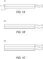
- an optical device 10 including a substrate 20; and an optical stack 30 of layers including metal oxides, as shown in FIG. 1A .
- an optical device 100 including an optical stack 30 of layers including metal oxides; and a surface treating agent 40, as shown in FIG. 1B .
- an optical device 110 including a substrate 20, an optical stack 30 of layers including metal oxides; and a surface treating agent 40, as shown in FIG. 1C .
- the optical device 10 can exhibit mechanical and environmental durability for use under harsh mechanical and environmental conditions.
- the disclosed optical devices 10, 100, 110 can have at least one of the following properties: improved mechanical durability, improved environmental durability, improved chemical durability, smudge resistance, and controlled surface roughness.
- Improved mechanical durability includes durability in view of scratches, abrasion, dents, breakage, wear, etc.
- Improved environmental durability includes durability in a variety of environmental conditions, such as high temperature, high humidity, salt, fog, UV exposure.
- the substrate 20 of the optical device 10, 110 can be any material capable of being coated.
- Non-limiting examples of a substrate 20 include plastics, synthetic sapphire, glass, synthetic diamond, optical ceramic materials, optical quality polymers, and light transmitting substrates with absorption spectra as required by the functional application of the optical device 10, 110, such as silicon.
- Optical quality polymers include polycarbonates, acrylates, and cyclic olefin polymers.
- Various types of glass can be used including chemically strengthened glass.
- the substrate 20 can have a first surface 21 and a second surface 22 opposite the first surface, as shown in FIG. 1A .
- the optical stack 30 of optical devices, 10, 100, 110 can include layers of metal oxides.
- metal oxides include oxides include titanium dioxide (TiO 2 ), zirconium dioxide (ZrO 2 ), niobium pentoxide (Nb 2 O 5 ), tantalum pentoxide (Ta 2 O 5 ), hafnium dioxide (HfO 2 ), aluminum trioxide (Al 2 O 3 ), silicon dioxide (SiO 2 ), scandium trioxide (Sc 2 O 3 ), yttrium trioxide (Y 2 O 3 ), magnesium dioxide (MgO 2 ), SiAlO x , SiO x N y , SiAlO x N y , and mixtures thereof.
- the optical stack 30 of layers can include two layers of alternating different metal oxides.
- the optical stack 30 of layers can include two layers of alternating different metal oxides with a top layer of aluminum trioxide.
- the optical stack 30 of layers can include two layers of alternating different metal oxides with a top layer of silicon dioxide.
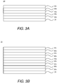
- FIGs. 2A and 2B illustrate an optical device10 including a substrate 20 of glass and an optical stack 30.
- the optical stack 30 includes alternating layers of two different metal oxides for a total of four layers ( FIG. 2A ).
- the optical stack 30 can be as follows: NbTiO x 11.28 nm (30a)/ SiO 2 34.44 nm (30b)/ NbTiO x 105.43 nm (30a)/ SiO 2 84.45 nm (30b).
- the percent reflectance for this optical device 10 can be seen in FIG. 5 .
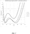
- the optical stack 30 can be as follows: NbTiO x 14.72 nm (30a)/ Al 2 O 3 25.24 nm (30b)/ NbTiO x 65.31 nm (30a)/ Al 2 O 3 71.91 nm (30b). The percent reflectance for this optical device 10 can be seen in FIG. 7 .
- the optical stack 30 can be as follows: Ta 2 O 5 13.40 nm (30a)/ Al 2 O 3 37.40 nm (30b)/ Ta 2 O 5 61.24 nm (30a)/ Al 2 O 3 75.54 nm (30b). The percent reflectance for this optical device 10 can be seen in FIG. 8 .
- the optical stack 30 includes alternating layers of two different metal oxides for a total of twelve layers ( FIG. 2B ).
- the optical stack 30 can be as follows: NbTiO x 8.66 nm (30a)/ Al 2 O 3 40.25 nm (30b)/ NbTiO x 93.32 nm (30a)/ Al 2 O 3 12.58 nm (30b) / NbTiO x 23.32 nm (30a)/ Al 2 O 3 28.76 nm (30b)/ NbTiO x 109.23 nm (30a)/ Al 2 O 3 85.50 nm (30b) / NbTiO x 9.12 nm (30a)/ Al 2 O 3 37.46 nm (30b)/ NbTiO x 54.62 nm (30a)/ Al 2 O 3 74.34 nm (30b).
- the percent reflectance for this optical device 10 can be seen in FIG. 10 .
- a surface treating agent 40 can
- FIGs. 3A and 3B illustrate an optical device 10 including a substrate 20 of glass and an optical stack 30.
- the optical stack 30 includes alternating layers of two different metal oxides with a top layer having a different metal oxide, such as either aluminum trioxide or silicon dioxide.
- FIG. 3A illustrates an optical stack 30 as follows: NbTiO x 13.78 nm (30a)/ SiO 2 33.93 nm (30b)/ NbTiO x 116.58 nm (30a)/ SiO 2 26.70 nm (30b) / Al 2 O 3 50.00 nm (30c).
- the percent reflectance for this optical device 10 can be seen in FIG. 6 .
- FIG. 6 The percent reflectance for this optical device 10 can be seen in FIG. 6 .
- 3B illustrates an optical stack 30 as follows: NbTiO x 11.47 nm (30a)/ SiO 2 35.02 nm (30b)/ NbTiO x 120.91 nm (30a)/ SiO 2 28.13 nm (30b) / NbTiO x 36.31 nm (30a)/ SiO 2 16.98 nm (30b)/ NbTiO x 62.16 nm (30a)/ SiO 2 24.08 nm (30b) / Al 2 O 3 50.00 nm (30c).
- the percent reflectance for this optical device 10 can be seen in FIG. 9 .
- a surface treating agent 40 can be applied to each of the top layers of the optical stack 30 in each of FIGs. 3A and 3B .
- the optical stack 30 of layers can include coatings with various functional properties.
- the optical stack 30 of layers can include more than one functional property.
- the optical stack 30 of layers can include at least one of an anti-reflective coating, a bandpass filter coating, notch filter coating, a dichroic filter coating, a mirror coating, and combinations thereof. It is noted that the disclosed coatings can contain more than one layer, for example, a bandpass filter coating can include multiple layers.
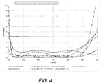
- FIG. 4 is a line graph illustrating the reflectance of the optical devices 10 illustrated in FIGS 2A-3B as compared to the substrate 20 glass without an optical stack 30.
- FIGs. 1A-3B illustrate various optical devices 10, 100, 110 contemplated herein. These are exemplary in nature. It should be appreciated that the order of the layers and the number of the layers in the optical stack 30 can vary. The layers of the optical stack 30 are described more fully below.
- a layer in the optical stack 30 can be an antireflective coating.
- the antireflective coating can be a dielectric stack and can reduce the light reflection on an interface with the substrate 20.
- Suitable dielectrics for forming the dielectric stack include metal oxides such as TiO 2 , Ta 2 O 5 , ZrO 2 , and SiO 2 , which are optically isotropic and can exhibit high transparency in the visible wavelength spectrum range (e.g., from 400nm to 700nm).
- the antireflective coating can be a stack including a first plurality of dielectric layers having a first refractive index, such as a low refractive index, for example, SiO 2 or magnesium fluoride (MgF 2 ), interleaved with at least a second plurality of dielectric layers having a second refractive index, such as a high refractive index.
- first refractive index such as a low refractive index, for example, SiO 2 or magnesium fluoride (MgF 2
- MgF 2 magnesium fluoride
- high refractive index materials include niobium oxide, tantalum oxide, aluminum oxide, titanium oxide, zirconium oxide, and their combinations.
- the antireflective coating can be formed of a stack of layers of NbTiO x , SiO 2 , or the like.
- the optical device 10, 100, 110 can include an optical stack 30 including a bandpass filter.
- the bandpass filter can be realized by a full stack of dielectric low and high refractive materials. Each layer can be deposited as a quarter-wave (QW) thickness at the wavelength of the desired filter.
- Each partial-reflector which may be comprised of only a single layer, is called a quarter-wave stack (QWS).
- QWS quarter-wave stack
- the bandwidth of the filter is a function of the reflectance of quarter-wave stacks in the structure.
- the center wavelength of the pass-band is determined by the thickness of the spacer dielectric material.
- the dielectric materials used for the quarter and/or half-wave layers have indices of refraction in the range 1.3 to beyond 4.0.
- some suitable materials are: Magnesium Fluoride (1.38), Thorium Fluoride (1.47), Cryolite (1.35), Silicon Dioxide (1.46), Aluminum Oxide (1.63), Hafnium Oxide (1.85), Tantalum Pentoxide (2.05), Niobium Oxide (2.19), Zinc Sulphide (2.27), Titanium Oxide (2.37), Silicon (3.5), Germanium (4.0), and Lead Telluride (5.0).
- Other dielectric materials would serve as well.
- the fully dielectric band pass filter can also combine anti-reflective properties.
- the bandpass filter can be a polymeric coating containing an appropriate mixture of dyes to create required absorbance or a combination of dielectric and polymeric structures.
- the bandpass filter can allow a wavelength of light at which a sensor operates pass and can eliminate all other wavelengths.
- the bandpass filter can block wavelengths in the visible and near IR spectral range, such as from about 400 to about 850 nm, and can transmit wavelengths above 850 nm. In this manner, the bandpass filter can reduce and/or eliminate unwanted radiation from reaching the optical device 10, 100, 110.
- the optical stack 30 can be applied to the substrate 20 using any deposition or coating process, including a long throw magnetron sputtering process.
- the optical stack 30 can have at least one of the following properties: high density, strong interfacial adhesion strength, lack of structural defects, etc.
- the optical stack 30 can include a top layer of either aluminum trioxide or silicon dioxide.
- the optical device 10, 100, 110 can include a layer of sputter deposited dense aluminum trioxide that can act as a layer of synthetic sapphire.
- the final optical device 10, 100, 110 can offer increased resistance to mechanical scratching, abrasion, impact.
- a top layer of aluminum trioxide in the optical stack 30 can provide additional mechanical durability and increase scratch resistance.
- a bottom layer of aluminum trioxide in the optical stack 30, such as the first layer interfacing with the substrate 20, such as glass, can act as an ion migration barrier.
- the bottom layer of aluminum trioxide can be present at a thickness ranging from about 0.5 ⁇ m to about 20 ⁇ m, for example from about 1 ⁇ m to about 15 ⁇ m, and as a further example, from about 3 ⁇ m to about 12 ⁇ m. This thickness can provide mechanical strength.
- the optical device 10, 100, 110 disclosed herein can include a surface treating agent 40.
- the surface treating agent 40 can include a perfluoro(poly)ether group-containing silane compound which can form a layer having water-repellency, oil-repellency and antifouling property as well as high friction durability.
- the perfluoro(poly)ether group-containing silane compound can have the following formula (1): wherein: Rf can be an alkyl group having 1 to 10 carbon atoms which may be substituted by one or more fluorine atoms; PFPE is (OC 4 F 8 ) a -(OC 3 F 6 ) b -(OC 2 F 4 ) c -(OCF 2 ) d -; wherein a, b, c and d can each be independently an integer of 0 to 200, the sum of a, b, c and d is 1 or more, and the occurrence order of the respective repeating units in parentheses with the subscript a, b, c or d is not limited in the formula; Q can be an oxygen atom or a divalent organic group; R 1 can be a hydrogen atom or an alkyl group having 1 to 22 carbon atoms; R 2 can each be independently a hydrogen atom or an inert monovalent organic group; X can be a
- alkyl group having 1 to 10 carbon atoms in the alkyl group having 1 to 10 carbon atoms which can be substituted by one or more fluorine atoms can be a straight or branched alkyl group having 1-10 carbon atoms, for example a straight or branched alkyl group having 1-3 carbon atoms, and as a further example a straight alkyl group having 1-3 carbon atoms.
- Rf can be an alkyl group having 1 to 10 carbon atoms which can be substituted by one or more fluorine atoms, for example a perfluoroalkyl group having 1 to 10 carbon atoms or CF 2 H-C 1-9 perfluoroalkylene group, and as a further example a perfluoroalkyl group having 1 to 10 carbon atoms.
- the perfluoroalkyl group having 1 to 10 carbon atoms can be a straight or branched perfluoroalkyl group having 1-10 carbon atoms, for example a straight or branched perfluoroalkyl group having 1-3 carbon atoms, and as a further example a straight perfluoroalkyl group having 1-3 carbon atoms, such as -CF 3 , -CF 2 CF 3 or -CF 2 CF 2 CF 3 .
- the surface treating agent 40 can be applied to the optical stack 30 using a wet coating method or a dry coating method.
- a wet coating method include dip coating, spin coating, flow coating, spray coating, roll coating, gravure coating, and a similar method.
- Non-limiting examples of a dry coating method include deposition (usually, vacuum deposition), sputtering, chemical vapor deposition (CVD) and a similar method.
- the specific examples of the deposition method (usually, vacuum deposition) include resistance heating, electron beam, high-frequency heating, ion beam, and a similar method.
- the specific examples of the CVD method include plasma-CVD, optical CVD, thermal CVD and a similar method.
- the surface treating agent 40 can have a high surface slip property and high friction durability. Furthermore, this surface treating agent 40 can have water-repellency, oil-repellency, antifouling property (for example, preventing from adhering a fouling such as fingerprints), waterproof property (preventing infiltration of water into electrical components, and the like), surface slip property (or lubricity, for example, wiping property of a fouling such as fingerprints and excellent tactile feeling in a finger) depending on a composition of the surface treating agent used, in addition to high friction durability.
- water-repellency for example, preventing from adhering a fouling such as fingerprints
- waterproof property preventing infiltration of water into electrical components, and the like
- surface slip property or lubricity, for example, wiping property of a fouling such as fingerprints and excellent tactile feeling in a finger
- the optical device 110 can include a substrate 20 having on a first surface 21 an optical stack 30, and optionally a surface treating agent 40.
- the substrate 20 can also have on a second surface 22 an optional transparent optical conductor 50.
- the transparent optical conductor 50 can include any transparent material that can conduct a charge.
- the transparent optical conductor 50 can include indium tin oxide or indium titanium oxide.
- the optical device 110 can further include a hydrophilic layer 60 on the transparent optical conductor 50.
- the hydrophilic layer 60 can be present between the substrate 20 and a sensor (not shown). In this manner, the hydrophilic layer 60 can prevent or reduce condensation or fogging.
- the hydrophilic layer 60 e.g., having a contact angle with water of less than 10 °
- can also be a super-hydrophilic layer e.g., having a contact angle with water of about 0 °.
- Non-limiting examples of materials useful in the hydrophilic layer 60 or super-hydrophilic layer include polyurethanes, siloxanes, metal oxides, polyglycols, and mixtures thereof.
- the hydrophilic layer 60 can be applied as a contiguous film having a thickness ranging from about 0.2 microns to about 20 microns, for example from about 0.5 to about 15 microns, and as a further example, from about 0.7 to about 13 microns.
- the materials used to form the hydrophilic layer can be nanoparticles applied with deposition processes to yield the disclosed thicknesses.
- Deposition processes include, but are not limited to, physical vapor deposition, such as evaporation atomic layer deposition, plasma enhanced chemical vapor deposition; and wet-chemical deposition processes, such as spraying, spin-coating, and roll coating techniques, for example, gravure, and transfer; etc.
- the optical devices 10, 100, 110 disclosed herein can also include a secondary visual feature.
- the secondary visual feature can be seen by a user.
- Non-limiting examples of a secondary visual feature include a logo, symbol, number, pattern, color, etc.
- a method of making an optical device 10 is also disclosed.
- the method of making the optical device 10 can include providing a substrate; and forming on the substrate a stack of layers including metal oxides using a long throw magnetron sputtering process.
- the method can also include applying a surface treating agent onto a top layer of the stack of layers of the optical device.
- the method of making an optical device 10 can also include forming a stack of layers including metal oxides by a long throw magnetron sputtering process; and applying a surface treating agent onto a top layer of the stack of layers to form the optical device.
- the method can also include applying the optical device onto a substrate.
- the long throw magnetron sputtering process used in the methods of making includes depositing a film in a chamber having a long throw distance between the target and the magnet array disposed adjacent the substrate.
- the long throw process may optionally include a grounded collimator and a circular magnet array.
- a long throw sputtering chamber can include a vacuum chamber enclosure wall having a gas inlet and an exhaust outlet connected to an exhaust pump.
- a substrate support pedestal can be disposed at one end of the chamber, and the sputtering target can be mounted to the other end of the chamber.
- the target can be electrically isolated from the enclosure wall by an insulator, and the enclosure wall can be grounded, so that a negative voltage may be maintained on the target with respect to the grounded enclosure wall.
- a substrate 20 can be positioned on the support pedestal at a long throw distance from the target of at least 50 mm, for example at about 80 to 175 mm.
- An optical device comprising: an optical stack of layers including metal oxides; and a surface treating agent.
- a method of making an optical device comprising: forming an optical stack of layers including metal oxides by a long throw magnetron sputtering process; and applying a surface treating agent onto a top layer of the optical stack of layers to form the optical device.
Landscapes
- Physics & Mathematics (AREA)
- General Physics & Mathematics (AREA)
- Optics & Photonics (AREA)
- Chemical & Material Sciences (AREA)
- Chemical Kinetics & Catalysis (AREA)
- Organic Chemistry (AREA)
- Life Sciences & Earth Sciences (AREA)
- Engineering & Computer Science (AREA)
- General Chemical & Material Sciences (AREA)
- Geochemistry & Mineralogy (AREA)
- Materials Engineering (AREA)
- Inorganic Chemistry (AREA)
- Surface Treatment Of Optical Elements (AREA)
- Surface Treatment Of Glass (AREA)
- Laminated Bodies (AREA)
- Optical Filters (AREA)
- Optical Integrated Circuits (AREA)
Abstract
Description
- The present application claims priority to
U.S. Provisional Application No. 62/642,473, filed on March 13, 2018 - The present disclosure generally relates to an optical device including a substrate; and an optical stack of layers including metal oxides. An optical device can also include an optical stack of layers including metal oxides; and a surface treating agent. An optical device can also include a substrate; an optical stack of layers including metal oxides; and a surface treating agent. A method of making optical devices is also disclosed.
- Optical devices are becoming increasingly important with the advent of semi-autonomous, autonomous, remotely controlled vehicles, and smart phones. However, the use of optical devices raises a concern as to whether the optical devise can withstand mechanical, optical, and environmental factors that could damage or adversely impact the function of the optical device. For example, using a smartphone near an ocean environment exposes the glass of the optical device to various environmental conditions, as well as the mechanical hazards, such as dropping the phone, abrasion from sand, etc. Optical devices are increasingly used in areas that require additional protections for the device in order to ensure durability and functionality.
- In an aspect, there is disclosed an optical device including a substrate; and an optical stack of layers including metal oxides.
- The optical device may further comprise a surface treating agent.
- The substrate may be glass.
- The optical stack of layers may include at least one of an anti-reflective coating, a bandpass filter coating, notch filter coating, a dichroic filter coating, a mirror coating, and combinations thereof.
- The metal oxides may include titanium dioxide (TiO2), zirconium dioxide (ZrO2), niobium pentoxide (Nb2O5), tantalum pentoxide (Ta2O5), hafnium dioxide (HfO2), aluminum trioxide (Al2O3), silicon dioxide (SiO2), scandium trioxide (Sc2O3), yttrium trioxide (Y2O3), magnesium dioxide (MgO2), SiAlOx, SiOxNy, SiAlOxNy, and mixtures thereof.
- The optical stack of layers may include two layers of alternating different metal oxides.
- The optical stack of layers may include two layers of alternating different metal oxides with a top layer of aluminum trioxide.
- The optical stack of layers may include two layers of alternating different metal oxides with a bottom layer of aluminum trioxide.
- Optionally, the metal oxide may be aluminum trioxide, wherein the aluminum trioxide is a mechanical and chemical barrier.
- The optical stack of layers may include two layers of alternating different metal oxides with a top layer of silicon dioxide.
- The surface treating agent may include a perfluoro(poly)ether group-containing silane compound.
- The optical device may exhibit mechanical and environmental durability for use under harsh mechanical and environmental conditions.
- The substrate may have a first surface including an optical stack and a surface treating agent, and the substrate may have a second surface including a transparent optical conductor.
- Optionally, the transparent optical conductor includes indium tin oxide or indium titanium oxide.
- The optical device may further comprise on the second surface a hydrophilic layer or super-hydrophilic layer.
- The hydrophilic layer may include a material chosen from polyurethanes, siloxanes, metal oxides, polyglycols, and mixtures thereof.
- In another aspect, there is disclosed an optical device including an optical stack of layers including metal oxides; and a surface treating agent.
- Optionally, the optical device further comprises a substrate.
- In another aspect, there is disclosed method of making an optical device, comprising forming an optical stack of layers including metal oxides by a long throw magnetron sputtering process; and applying a surface treating agent onto a top layer of the optical stack of layers to form the optical device.
- The method may further comprise applying the optical device onto a substrate.
- Additional features and advantages of various embodiments will be set forth, in part, in the description that follows, and will, in part, be apparent from the description, or may be learned by the practice of various embodiments. The objectives and other advantages of various embodiments will be realized and attained by means of the elements and combinations particularly pointed out in the description herein.
- The present disclosure in its several aspects and embodiments can be more fully understood from the detailed description and the accompanying drawings, wherein:
-
FIGs. 1A-1C illustrate a cross-section of an optical device according to various aspects of the invention; -
FIG. 2A is a cross-section of an optical device according to another aspect of the invention; -
FIG. 2B is a cross-section of an optical device according to another aspect of the invention; -
FIG. 3A is a cross-section of an optical device according to another aspect of the invention; -
FIG. 3B is a cross-section of an optical device according to another aspect of the invention; -
FIG. 4 is a line graph illustrating the reflectance percentage of the optical devices illustrated inFIGS. 2A, 2B ,3A, and 3B at an angle of incidence of 0°, according to another aspect of the invention; -
FIG. 5 is a line graph illustrating the reflectance percentage of an optical device at various angles of incident (AOI) according to an aspect of the invention; -
FIG. 6 is a line graph illustrating the reflectance percentage of an optical device at various angles of incident (AOI) according to an aspect of the invention; -
FIG. 7 is a line graph illustrating the reflectance percentage of an optical device at various angles of incident (AOI) according to an aspect of the invention; -
FIG. 8 is a line graph illustrating the reflectance percentage of an optical device at various angles of incident (AOI) according to an aspect of the invention; -
FIG. 9 is a line graph illustrating the reflectance percentage of an optical device at various angles of incident (AOI) according to an aspect of the invention; -
FIG. 10 is a line graph illustrating the reflectance percentage of an optical device at various angles of incident (AOI) according to an aspect of the invention; and -
FIGs. 11A-B are each an optical device according to another aspect of the invention. - Throughout this specification and figures like reference numbers identify like elements.
- It is to be understood that both the foregoing general description and the following detailed description are exemplary and explanatory only, and are intended to provide an explanation of various embodiments of the present teachings. The layers/components shown in each Figure may be described with regard to a particular Figure, but it is understood that the description of a particular layer/component would be applicable to the equivalent layer/component in the other Figures.
- In its broad and varied embodiments, there is disclosed an
optical device 10 including asubstrate 20; and anoptical stack 30 of layers including metal oxides, as shown inFIG. 1A . There is also disclosed anoptical device 100 including anoptical stack 30 of layers including metal oxides; and asurface treating agent 40, as shown inFIG. 1B . Further, there is disclosed anoptical device 110 including asubstrate 20, anoptical stack 30 of layers including metal oxides; and asurface treating agent 40, as shown inFIG. 1C . Theoptical device 10 can exhibit mechanical and environmental durability for use under harsh mechanical and environmental conditions. - The disclosed
optical devices - Improved mechanical durability includes durability in view of scratches, abrasion, dents, breakage, wear, etc. Improved environmental durability includes durability in a variety of environmental conditions, such as high temperature, high humidity, salt, fog, UV exposure.
- The
substrate 20 of theoptical device substrate 20 include plastics, synthetic sapphire, glass, synthetic diamond, optical ceramic materials, optical quality polymers, and light transmitting substrates with absorption spectra as required by the functional application of theoptical device substrate 20 can have afirst surface 21 and asecond surface 22 opposite the first surface, as shown inFIG. 1A . - The
optical stack 30 of optical devices, 10, 100, 110 can include layers of metal oxides. Non-limiting examples of metal oxides include oxides include titanium dioxide (TiO2), zirconium dioxide (ZrO2), niobium pentoxide (Nb2O5), tantalum pentoxide (Ta2O5), hafnium dioxide (HfO2), aluminum trioxide (Al2O3), silicon dioxide (SiO2), scandium trioxide (Sc2O3), yttrium trioxide (Y2O3), magnesium dioxide (MgO2), SiAlOx, SiOxNy, SiAlOxNy, and mixtures thereof. Theoptical stack 30 of layers can include two layers of alternating different metal oxides. Theoptical stack 30 of layers can include two layers of alternating different metal oxides with a top layer of aluminum trioxide. Theoptical stack 30 of layers can include two layers of alternating different metal oxides with a top layer of silicon dioxide. -
FIGs. 2A and 2B illustrate an optical device10 including asubstrate 20 of glass and anoptical stack 30. Theoptical stack 30 includes alternating layers of two different metal oxides for a total of four layers (FIG. 2A ). In an aspect, theoptical stack 30 can be as follows: NbTiOx 11.28 nm (30a)/ SiO2 34.44 nm (30b)/ NbTiOx 105.43 nm (30a)/ SiO2 84.45 nm (30b). The percent reflectance for thisoptical device 10 can be seen inFIG. 5 . In another aspect, theoptical stack 30 can be as follows: NbTiOx 14.72 nm (30a)/ Al2O3 25.24 nm (30b)/ NbTiOx 65.31 nm (30a)/ Al2O3 71.91 nm (30b). The percent reflectance for thisoptical device 10 can be seen inFIG. 7 . In another aspect, theoptical stack 30 can be as follows: Ta2O5 13.40 nm (30a)/ Al2O3 37.40 nm (30b)/ Ta2O5 61.24 nm (30a)/ Al2O3 75.54 nm (30b). The percent reflectance for thisoptical device 10 can be seen inFIG. 8 . Theoptical stack 30 includes alternating layers of two different metal oxides for a total of twelve layers (FIG. 2B ). In an aspect, theoptical stack 30 can be as follows: NbTiOx 8.66 nm (30a)/ Al2O3 40.25 nm (30b)/ NbTiOx 93.32 nm (30a)/ Al2O3 12.58 nm (30b) / NbTiOx 23.32 nm (30a)/ Al2O3 28.76 nm (30b)/ NbTiOx 109.23 nm (30a)/ Al2O3 85.50 nm (30b) / NbTiOx 9.12 nm (30a)/ Al2O3 37.46 nm (30b)/ NbTiOx 54.62 nm (30a)/ Al2O3 74.34 nm (30b). The percent reflectance for thisoptical device 10 can be seen inFIG. 10 . Asurface treating agent 40 can be applied to each of the top layers of theoptical stack 30 in each ofFIGs. 2A and 2B . -
FIGs. 3A and 3B illustrate anoptical device 10 including asubstrate 20 of glass and anoptical stack 30. Theoptical stack 30 includes alternating layers of two different metal oxides with a top layer having a different metal oxide, such as either aluminum trioxide or silicon dioxide.FIG. 3A illustrates anoptical stack 30 as follows: NbTiOx 13.78 nm (30a)/ SiO2 33.93 nm (30b)/ NbTiOx 116.58 nm (30a)/ SiO2 26.70 nm (30b) / Al2O3 50.00 nm (30c). The percent reflectance for thisoptical device 10 can be seen inFIG. 6 .FIG. 3B illustrates anoptical stack 30 as follows: NbTiOx 11.47 nm (30a)/ SiO2 35.02 nm (30b)/ NbTiOx 120.91 nm (30a)/ SiO2 28.13 nm (30b) / NbTiOx 36.31 nm (30a)/ SiO2 16.98 nm (30b)/ NbTiOx 62.16 nm (30a)/ SiO2 24.08 nm (30b) / Al2O3 50.00 nm (30c). The percent reflectance for thisoptical device 10 can be seen inFIG. 9 . Asurface treating agent 40 can be applied to each of the top layers of theoptical stack 30 in each ofFIGs. 3A and 3B . - The
optical stack 30 of layers can include coatings with various functional properties. In an aspect, theoptical stack 30 of layers can include more than one functional property. Theoptical stack 30 of layers can include at least one of an anti-reflective coating, a bandpass filter coating, notch filter coating, a dichroic filter coating, a mirror coating, and combinations thereof. It is noted that the disclosed coatings can contain more than one layer, for example, a bandpass filter coating can include multiple layers.FIG. 4 is a line graph illustrating the reflectance of theoptical devices 10 illustrated inFIGS 2A-3B as compared to thesubstrate 20 glass without anoptical stack 30. -
FIGs. 1A-3B illustrate variousoptical devices optical stack 30 can vary. The layers of theoptical stack 30 are described more fully below. - A layer in the
optical stack 30 can be an antireflective coating. The antireflective coating can be a dielectric stack and can reduce the light reflection on an interface with thesubstrate 20. Suitable dielectrics for forming the dielectric stack include metal oxides such as TiO2, Ta2O5, ZrO2, and SiO2, which are optically isotropic and can exhibit high transparency in the visible wavelength spectrum range (e.g., from 400nm to 700nm). The antireflective coating can be a stack including a first plurality of dielectric layers having a first refractive index, such as a low refractive index, for example, SiO2 or magnesium fluoride (MgF2), interleaved with at least a second plurality of dielectric layers having a second refractive index, such as a high refractive index. Non-limiting examples of high refractive index materials include niobium oxide, tantalum oxide, aluminum oxide, titanium oxide, zirconium oxide, and their combinations. The antireflective coating can be formed of a stack of layers of NbTiOx, SiO2, or the like. - The
optical device optical stack 30 including a bandpass filter. The bandpass filter can be realized by a full stack of dielectric low and high refractive materials. Each layer can be deposited as a quarter-wave (QW) thickness at the wavelength of the desired filter. Each partial-reflector, which may be comprised of only a single layer, is called a quarter-wave stack (QWS). The bandwidth of the filter is a function of the reflectance of quarter-wave stacks in the structure. The center wavelength of the pass-band is determined by the thickness of the spacer dielectric material. The dielectric materials used for the quarter and/or half-wave layers have indices of refraction in the range 1.3 to beyond 4.0. For example, some suitable materials are: Magnesium Fluoride (1.38), Thorium Fluoride (1.47), Cryolite (1.35), Silicon Dioxide (1.46), Aluminum Oxide (1.63), Hafnium Oxide (1.85), Tantalum Pentoxide (2.05), Niobium Oxide (2.19), Zinc Sulphide (2.27), Titanium Oxide (2.37), Silicon (3.5), Germanium (4.0), and Lead Telluride (5.0). Other dielectric materials would serve as well. Besides that, the fully dielectric band pass filter can also combine anti-reflective properties. - In an aspect, the bandpass filter can be a polymeric coating containing an appropriate mixture of dyes to create required absorbance or a combination of dielectric and polymeric structures.
- The bandpass filter can allow a wavelength of light at which a sensor operates pass and can eliminate all other wavelengths. For example, the bandpass filter can block wavelengths in the visible and near IR spectral range, such as from about 400 to about 850 nm, and can transmit wavelengths above 850 nm. In this manner, the bandpass filter can reduce and/or eliminate unwanted radiation from reaching the
optical device - The
optical stack 30 can be applied to thesubstrate 20 using any deposition or coating process, including a long throw magnetron sputtering process. Theoptical stack 30 can have at least one of the following properties: high density, strong interfacial adhesion strength, lack of structural defects, etc. Theoptical stack 30 can include a top layer of either aluminum trioxide or silicon dioxide. - An
optical stack 30 with a terminal layer of silicon dioxide can have a high surface concentration of Si=O bonds and can provide reactive sites for attachment of asurface treating agent 40. Additionally, this creates an efficient barrier for ions diffusing from asubstrate 20, such as glass. In particular, the presence of an ion diffusion barrier can reduce the possibility of potassium ions used in chemical glass strengthening from migrating to the interface between the top layer of the silicon dioxide and thesurface treating agent 40. This can have a further effect in reducing the risk of any potassium ions contributing to hydrolytic degradation of siloxanes. - In an aspect, the
optical device optical stack 30 and depending upon the thickness of the aluminum trioxide layer, the finaloptical device optical stack 30 can provide additional mechanical durability and increase scratch resistance. As another example, a bottom layer of aluminum trioxide in theoptical stack 30, such as the first layer interfacing with thesubstrate 20, such as glass, can act as an ion migration barrier. In an aspect, the bottom layer of aluminum trioxide can be present at a thickness ranging from about 0.5 µm to about 20 µm, for example from about 1 µm to about 15 µm, and as a further example, from about 3 µm to about 12 µm. This thickness can provide mechanical strength. - The
optical device surface treating agent 40. Thesurface treating agent 40 can include a perfluoro(poly)ether group-containing silane compound which can form a layer having water-repellency, oil-repellency and antifouling property as well as high friction durability. - The perfluoro(poly)ether group-containing silane compound can have the following formula (1):

Rf can be an alkyl group having 1 to 10 carbon atoms which may be substituted by one or more fluorine atoms; PFPE is (OC4F8)a-(OC3F6)b-(OC2F4)c-(OCF2)d-; wherein a, b, c and d can each be independently an integer of 0 to 200, the sum of a, b, c and d is 1 or more, and the occurrence order of the respective repeating units in parentheses with the subscript a, b, c or d is not limited in the formula; Q can be an oxygen atom or a divalent organic group; R1 can be a hydrogen atom or an alkyl group having 1 to 22 carbon atoms; R2 can each be independently a hydrogen atom or an inert monovalent organic group; X can be a hydroxyl group or a hydrolysable group; Y can be a hydrogen atom or a halogen atom; Z can be a fluorine atom or a fluoroalkyl group having 1 to 5 carbon atoms; e can be an integer from 0 to 3; f can be 0 or 1; g can be an integer from 1 to 10; h can be an integer from 0 to 3; and n can be an integer from 1 to 3, wherein 80 mol % or more of the perfluoro(poly)ether group containing silane compound contained in the surface-treating agent is a compound wherein g is 2 or more. - The "alkyl group having 1 to 10 carbon atoms" in the alkyl group having 1 to 10 carbon atoms which can be substituted by one or more fluorine atoms can be a straight or branched alkyl group having 1-10 carbon atoms, for example a straight or branched alkyl group having 1-3 carbon atoms, and as a further example a straight alkyl group having 1-3 carbon atoms.
- The above-described Rf can be an alkyl group having 1 to 10 carbon atoms which can be substituted by one or more fluorine atoms, for example a perfluoroalkyl group having 1 to 10 carbon atoms or CF2H-C1-9 perfluoroalkylene group, and as a further example a perfluoroalkyl group having 1 to 10 carbon atoms.
- The perfluoroalkyl group having 1 to 10 carbon atoms can be a straight or branched perfluoroalkyl group having 1-10 carbon atoms, for example a straight or branched perfluoroalkyl group having 1-3 carbon atoms, and as a further example a straight perfluoroalkyl group having 1-3 carbon atoms, such as -CF3, -CF2CF3 or -CF2CF2CF3.
- The
surface treating agent 40 can be applied to theoptical stack 30 using a wet coating method or a dry coating method. Non-limiting examples of a wet coating method include dip coating, spin coating, flow coating, spray coating, roll coating, gravure coating, and a similar method. Non-limiting examples of a dry coating method include deposition (usually, vacuum deposition), sputtering, chemical vapor deposition (CVD) and a similar method. The specific examples of the deposition method (usually, vacuum deposition) include resistance heating, electron beam, high-frequency heating, ion beam, and a similar method. The specific examples of the CVD method include plasma-CVD, optical CVD, thermal CVD and a similar method. - The
surface treating agent 40 can have a high surface slip property and high friction durability. Furthermore, thissurface treating agent 40 can have water-repellency, oil-repellency, antifouling property (for example, preventing from adhering a fouling such as fingerprints), waterproof property (preventing infiltration of water into electrical components, and the like), surface slip property (or lubricity, for example, wiping property of a fouling such as fingerprints and excellent tactile feeling in a finger) depending on a composition of the surface treating agent used, in addition to high friction durability. - As shown in
FIG. 11A , theoptical device 110 can include asubstrate 20 having on afirst surface 21 anoptical stack 30, and optionally asurface treating agent 40. Thesubstrate 20 can also have on asecond surface 22 an optional transparentoptical conductor 50. The transparentoptical conductor 50 can include any transparent material that can conduct a charge. For example, the transparentoptical conductor 50 can include indium tin oxide or indium titanium oxide. - As shown in
FIG. 11B , theoptical device 110 can further include ahydrophilic layer 60 on the transparentoptical conductor 50. In particular, thehydrophilic layer 60 can be present between thesubstrate 20 and a sensor (not shown). In this manner, thehydrophilic layer 60 can prevent or reduce condensation or fogging. The hydrophilic layer 60 (e.g., having a contact angle with water of less than 10 °) can also be a super-hydrophilic layer (e.g., having a contact angle with water of about 0 °). Non-limiting examples of materials useful in thehydrophilic layer 60 or super-hydrophilic layer include polyurethanes, siloxanes, metal oxides, polyglycols, and mixtures thereof. Thehydrophilic layer 60 can be applied as a contiguous film having a thickness ranging from about 0.2 microns to about 20 microns, for example from about 0.5 to about 15 microns, and as a further example, from about 0.7 to about 13 microns. The materials used to form the hydrophilic layer can be nanoparticles applied with deposition processes to yield the disclosed thicknesses. Deposition processes include, but are not limited to, physical vapor deposition, such as evaporation atomic layer deposition, plasma enhanced chemical vapor deposition; and wet-chemical deposition processes, such as spraying, spin-coating, and roll coating techniques, for example, gravure, and transfer; etc. - In another aspect, the
optical devices - A method of making an
optical device 10 is also disclosed. The method of making theoptical device 10 can include providing a substrate; and forming on the substrate a stack of layers including metal oxides using a long throw magnetron sputtering process. The method can also include applying a surface treating agent onto a top layer of the stack of layers of the optical device. - The method of making an
optical device 10 can also include forming a stack of layers including metal oxides by a long throw magnetron sputtering process; and applying a surface treating agent onto a top layer of the stack of layers to form the optical device. The method can also include applying the optical device onto a substrate. - The long throw magnetron sputtering process used in the methods of making includes depositing a film in a chamber having a long throw distance between the target and the magnet array disposed adjacent the substrate. The long throw process may optionally include a grounded collimator and a circular magnet array. A long throw sputtering chamber can include a vacuum chamber enclosure wall having a gas inlet and an exhaust outlet connected to an exhaust pump. A substrate support pedestal can be disposed at one end of the chamber, and the sputtering target can be mounted to the other end of the chamber. The target can be electrically isolated from the enclosure wall by an insulator, and the enclosure wall can be grounded, so that a negative voltage may be maintained on the target with respect to the grounded enclosure wall. In operation, a
substrate 20 can be positioned on the support pedestal at a long throw distance from the target of at least 50 mm, for example at about 80 to 175 mm. - An optical device, comprising: an optical stack of layers including metal oxides; and a surface treating agent. The optical device of claim 17, further comprising a substrate.
- A method of making an optical device, comprising: forming an optical stack of layers including metal oxides by a long throw magnetron sputtering process; and applying a surface treating agent onto a top layer of the optical stack of layers to form the optical device. The method of claim 19, further comprising applying the optical device onto a substrate.
- From the foregoing description, those skilled in the art can appreciate that the present teachings can be implemented in a variety of forms. Therefore, while these teachings have been described in connection with particular embodiments and examples thereof, the true scope of the present teachings should not be so limited. Various changes and modifications may be made without departing from the scope of the teachings herein.
- This scope disclosure is to be broadly construed. It is intended that this disclosure disclose equivalents, means, systems and methods to achieve the devices, activities and mechanical actions disclosed herein. For each device, article, method, mean, mechanical element or mechanism disclosed, it is intended that this disclosure also encompass in its disclosure and teaches equivalents, means, systems and methods for practicing the many aspects, mechanisms and devices disclosed herein. Additionally, this disclosure regards a coating and its many aspects, features and elements. Such a device can be dynamic in its use and operation, this disclosure is intended to encompass the equivalents, means, systems and methods of the use of the device and/or article of manufacture and its many aspects consistent with the description and spirit of the operations and functions disclosed herein. The claims of this application are likewise to be broadly construed.
- The description of the inventions herein in their many embodiments is merely exemplary in nature and, thus, variations that do not depart from the gist of the invention are intended to be within the scope of the invention. Such variations are not to be regarded as a departure from the spirit and scope of the invention.
Claims (15)
- An optical device, comprising:a substrate; andan optical stack of layers including metal oxides.
- The optical device of claim 1, further comprising a surface treating agent.
- The optical device of claim 1, wherein the optical stack of layers includes at least one of an anti-reflective coating, a bandpass filter coating, notch filter coating, a dichroic filter coating, a mirror coating, and combinations thereof.
- The optical device of claim 1, wherein the metal oxides include titanium dioxide (TiO2), zirconium dioxide (ZrO2), niobium pentoxide (Nb2O5), tantalum pentoxide (Ta2O5), hafnium dioxide (HfO2), aluminum trioxide (Al2O3), silicon dioxide (SiO2), scandium trioxide (Sc2O3), yttrium trioxide (Y2O3), magnesium dioxide (MgO2), SiAlOx, SiOxNy, SiAlOxNy, and mixtures thereof.
- The optical device of claim 1, wherein the optical stack of layers includes two layers of alternating different metal oxides.
- The optical device of claim 1, wherein the optical stack of layers includes two layers of alternating different metal oxides with a top layer of aluminum trioxide.
- The optical device of claim 1, wherein the optical stack of layers includes two layers of alternating different metal oxides with a bottom layer of aluminum trioxide.
- The optical device of claim 1, wherein the metal oxide is aluminum trioxide, wherein the aluminum trioxide is a mechanical and chemical barrier.
- The optical device of claim 1, wherein the optical stack of layers includes two layers of alternating different metal oxides with a top layer of silicon dioxide.
- The optical device of claim 1, wherein the surface treating agent includes a perfluoro(poly)ether group-containing silane compound.
- The optical device of claim 1, wherein the optical device exhibits mechanical and environmental durability for use under harsh mechanical and environmental conditions.
- The optical device of claim 1, wherein the substrate has a first surface including an optical stack and a surface treating agent, and the substrate has a second surface including a transparent optical conductor.
- The optical device of claim 12, wherein the transparent optical conductor includes indium tin oxide or indium titanium oxide.
- The optical device of claim 12, further comprising on the second surface a hydrophilic layer or super-hydrophilic layer.
- The optical device of claim 15, wherein the hydrophilic layer includes a material chosen from polyurethanes, siloxanes, metal oxides, polyglycols, and mixtures thereof.
Applications Claiming Priority (1)
| Application Number | Priority Date | Filing Date | Title |
|---|---|---|---|
| US201862642473P | 2018-03-13 | 2018-03-13 |
Publications (2)
| Publication Number | Publication Date |
|---|---|
| EP3540478A2 true EP3540478A2 (en) | 2019-09-18 |
| EP3540478A3 EP3540478A3 (en) | 2019-12-18 |
Family
ID=65801902
Family Applications (1)
| Application Number | Title | Priority Date | Filing Date |
|---|---|---|---|
| EP19162293.5A Ceased EP3540478A3 (en) | 2018-03-13 | 2019-03-12 | Optical device including stack of optical layers with functional treatment |
Country Status (6)
| Country | Link |
|---|---|
| US (1) | US20190285775A1 (en) |
| EP (1) | EP3540478A3 (en) |
| JP (2) | JP2019174796A (en) |
| KR (2) | KR20190108073A (en) |
| CN (1) | CN110275230A (en) |
| TW (1) | TW201940450A (en) |
Cited By (4)
| Publication number | Priority date | Publication date | Assignee | Title |
|---|---|---|---|---|
| WO2022150095A1 (en) * | 2021-01-05 | 2022-07-14 | Ppg Industries Ohio, Inc. | Coated articles demonstrating anti-reflection, contaminant build-up resistance and uv durability |
| WO2023172938A1 (en) * | 2022-03-08 | 2023-09-14 | Viavi Solutions Inc. | Optical interference filter |
| WO2024200591A1 (en) * | 2023-03-31 | 2024-10-03 | Agp Worldwide Operations Gmbh | Glazing with low emissivity coating and enhanced bendability |
| US12429640B2 (en) | 2022-03-08 | 2025-09-30 | Viavi Solutions Inc. | Optical interference filter |
Families Citing this family (9)
| Publication number | Priority date | Publication date | Assignee | Title |
|---|---|---|---|---|
| CN111190244B (en) * | 2020-01-07 | 2021-10-08 | 杭州美迪凯光电科技股份有限公司 | Low-transmittance low-reflectivity coated sheet |
| JP7612377B2 (en) * | 2020-10-28 | 2025-01-14 | キヤノン株式会社 | Optical Components and Instruments |
| CN112609158B (en) * | 2020-11-20 | 2022-03-29 | 江苏北方湖光光电有限公司 | Visible infrared window antireflection film based on magnetron sputtering and preparation method |
| CN112578576B (en) * | 2020-12-02 | 2023-12-05 | 明月镜片股份有限公司 | Resin lens with high-hardness film structure and preparation method thereof |
| DE102021100093B4 (en) * | 2021-01-06 | 2025-10-23 | HELLA GmbH & Co. KGaA | Reflector element for a motor vehicle lighting device and method for its production |
| CN112764148A (en) * | 2021-02-05 | 2021-05-07 | 广州睿芯微电子有限公司 | Filtering unit and filtering chip applied to color imaging |
| EP4299542A4 (en) * | 2021-02-26 | 2025-03-05 | Agc Inc. | Transparent substrate with multilayer film and image display device |
| KR102561457B1 (en) * | 2021-08-11 | 2023-07-31 | 한국광기술원 | Structure for optical coating UV absorption and near-infrared transmission of optical module and coating method thereof, Appratus for optical coating UV absorption and near-infrared transmission of optical module |
| TWI920429B (en) * | 2022-06-03 | 2026-04-01 | 日商佳能股份有限公司 | Optical components and optical devices |
Citations (6)
| Publication number | Priority date | Publication date | Assignee | Title |
|---|---|---|---|---|
| EP1380857A1 (en) * | 2001-04-17 | 2004-01-14 | Sony Corporation | Antireflection film and antireflection layer-affixed plastic substrate |
| WO2013151984A2 (en) * | 2012-04-02 | 2013-10-10 | Guardian Industries Corp. | Heatable lens for luminaires, and/or methods of making the same |
| EP2033019B1 (en) * | 2006-06-28 | 2016-08-10 | ESSILOR INTERNATIONAL (Compagnie Générale d'Optique) | Optical article having a temperature-resistant anti-reflection coating with optimized thickness ratio of low index and high index layers |
| WO2016129699A1 (en) * | 2015-02-13 | 2016-08-18 | 日本板硝子株式会社 | Windshield |
| JP2016186539A (en) * | 2015-03-27 | 2016-10-27 | 株式会社豊田中央研究所 | Optical filter and optical measuring device |
| WO2018038114A1 (en) * | 2016-08-22 | 2018-03-01 | ホヤ レンズ タイランド リミテッド | Spectacle lens and spectacles |
Family Cites Families (25)
| Publication number | Priority date | Publication date | Assignee | Title |
|---|---|---|---|---|
| JP2993870B2 (en) * | 1995-08-10 | 1999-12-27 | 旭テクノグラス株式会社 | Multilayer interference film |
| US6800378B2 (en) * | 1998-02-19 | 2004-10-05 | 3M Innovative Properties Company | Antireflection films for use with displays |
| JP2001356201A (en) * | 2000-06-16 | 2001-12-26 | Canon Inc | Antifogging coating, optical component using the same, and method of forming antifogging coating |
| JP4577602B2 (en) * | 2001-07-31 | 2010-11-10 | 岩崎電気株式会社 | UV irradiation equipment |
| JP2003131206A (en) * | 2001-10-29 | 2003-05-08 | Nippon Electric Glass Co Ltd | Liquid crystal panel and counter substrate for liquid crystal panel |
| FR2841894B1 (en) * | 2002-07-03 | 2006-03-10 | Saint Gobain | TRANSPARENT SUBSTRATE HAVING ANTIREFLECTION COATING |
| CN101421641A (en) * | 2004-02-12 | 2009-04-29 | Api毫微制造及研究公司 | Films for optical use and methods of making such films |
| US7405880B2 (en) * | 2004-02-12 | 2008-07-29 | Api Nanofabrication And Research Corporation | Multilayer optical filter |
| JP2006124417A (en) * | 2004-10-26 | 2006-05-18 | Asahi Glass Co Ltd | Antifouling layer forming composition and antireflection laminate |
| US7838134B2 (en) * | 2004-11-23 | 2010-11-23 | Lawrence Livermore National Security, Llc | Durable silver mirror with ultra-violet thru far infra-red reflection |
| JP2007250342A (en) * | 2006-03-16 | 2007-09-27 | Matsushita Electric Works Ltd | Reflector for lighting equipment and lighting equipment |
| KR20090045648A (en) * | 2007-11-02 | 2009-05-08 | 이노베이션 앤드 인피니티 글로벌 코포레이션 | Ultra-low-resistance optical attenuated coating structure and manufacturing method |
| JP5358793B2 (en) * | 2008-08-20 | 2013-12-04 | 東海光学株式会社 | Optical article for infrared communication, manufacturing method thereof, and light receiving part for infrared communication |
| JP5489604B2 (en) * | 2009-01-14 | 2014-05-14 | ホーヤ レンズ マニュファクチャリング フィリピン インク | Method for manufacturing optical article |
| FR2954832A1 (en) * | 2009-12-31 | 2011-07-01 | Essilor Int | OPTICAL ARTICLE COMPRISING A TEMPORARY ANTIBUID COATING WITH IMPROVED DURABILITY |
| JP2013156523A (en) * | 2012-01-31 | 2013-08-15 | Topcon Corp | Substrate |
| JP2014065887A (en) * | 2012-09-10 | 2014-04-17 | Toyobo Co Ltd | Easily adhesive polyester film for optical use |
| US20150309216A1 (en) * | 2012-12-04 | 2015-10-29 | Essilor International (Compagnie Generale D'optique) | Method for coating an optical article with a topcoat using vacuum air plasma treatment |
| KR101910950B1 (en) * | 2013-07-05 | 2018-10-24 | 에씰로 앙터나시오날 | Optical article comprising an antireflective coating with a very low reflection in the visible region |
| JP2016179548A (en) * | 2015-03-23 | 2016-10-13 | 日本電気硝子株式会社 | Glass resin transparent laminate for window |
| CN114578461A (en) * | 2015-05-12 | 2022-06-03 | Agc株式会社 | Substrate with low reflection film |
| US11054556B2 (en) * | 2016-01-21 | 2021-07-06 | 3M Innovative Properties Company | Optical camouflage filters |
| US10170509B2 (en) * | 2016-02-12 | 2019-01-01 | Viavi Solutions Inc. | Optical filter array |
| JP6864170B2 (en) * | 2016-02-23 | 2021-04-28 | 東海光学株式会社 | ND filter and ND filter for camera |
| CA3027712A1 (en) * | 2016-06-13 | 2017-12-21 | Viavi Solutions Inc. | Protected item including a protective coating |
-
2019
- 2019-03-12 EP EP19162293.5A patent/EP3540478A3/en not_active Ceased
- 2019-03-12 KR KR1020190028383A patent/KR20190108073A/en not_active Ceased
- 2019-03-12 US US16/299,754 patent/US20190285775A1/en not_active Abandoned
- 2019-03-12 JP JP2019044521A patent/JP2019174796A/en active Pending
- 2019-03-13 CN CN201910190741.3A patent/CN110275230A/en active Pending
- 2019-03-13 TW TW108108249A patent/TW201940450A/en unknown
-
2021
- 2021-02-26 JP JP2021029413A patent/JP2021103305A/en active Pending
- 2021-08-26 KR KR1020210113454A patent/KR20210107605A/en not_active Ceased
Patent Citations (7)
| Publication number | Priority date | Publication date | Assignee | Title |
|---|---|---|---|---|
| EP1380857A1 (en) * | 2001-04-17 | 2004-01-14 | Sony Corporation | Antireflection film and antireflection layer-affixed plastic substrate |
| EP2033019B1 (en) * | 2006-06-28 | 2016-08-10 | ESSILOR INTERNATIONAL (Compagnie Générale d'Optique) | Optical article having a temperature-resistant anti-reflection coating with optimized thickness ratio of low index and high index layers |
| WO2013151984A2 (en) * | 2012-04-02 | 2013-10-10 | Guardian Industries Corp. | Heatable lens for luminaires, and/or methods of making the same |
| WO2016129699A1 (en) * | 2015-02-13 | 2016-08-18 | 日本板硝子株式会社 | Windshield |
| JP2016186539A (en) * | 2015-03-27 | 2016-10-27 | 株式会社豊田中央研究所 | Optical filter and optical measuring device |
| WO2018038114A1 (en) * | 2016-08-22 | 2018-03-01 | ホヤ レンズ タイランド リミテッド | Spectacle lens and spectacles |
| US20180299700A1 (en) * | 2016-08-22 | 2018-10-18 | Hoya Lens Thailand Ltd. | Spectacle lens and spectacles |
Cited By (5)
| Publication number | Priority date | Publication date | Assignee | Title |
|---|---|---|---|---|
| WO2022150095A1 (en) * | 2021-01-05 | 2022-07-14 | Ppg Industries Ohio, Inc. | Coated articles demonstrating anti-reflection, contaminant build-up resistance and uv durability |
| US12638615B2 (en) | 2021-01-05 | 2026-05-26 | Ppg Industries Ohio, Inc. | Coated articles demonstrating anti-reflection, contaminant build-up resistance and UV durability |
| WO2023172938A1 (en) * | 2022-03-08 | 2023-09-14 | Viavi Solutions Inc. | Optical interference filter |
| US12429640B2 (en) | 2022-03-08 | 2025-09-30 | Viavi Solutions Inc. | Optical interference filter |
| WO2024200591A1 (en) * | 2023-03-31 | 2024-10-03 | Agp Worldwide Operations Gmbh | Glazing with low emissivity coating and enhanced bendability |
Also Published As
| Publication number | Publication date |
|---|---|
| US20190285775A1 (en) | 2019-09-19 |
| TW201940450A (en) | 2019-10-16 |
| JP2021103305A (en) | 2021-07-15 |
| KR20210107605A (en) | 2021-09-01 |
| KR20190108073A (en) | 2019-09-23 |
| JP2019174796A (en) | 2019-10-10 |
| EP3540478A3 (en) | 2019-12-18 |
| CN110275230A (en) | 2019-09-24 |
Similar Documents
| Publication | Publication Date | Title |
|---|---|---|
| US20190285775A1 (en) | Optical device including stack of optical layers with functional treatment | |
| AU2002301541B2 (en) | Optical element having antireflection film | |
| CN107918167B (en) | Substrate with antiglare film, liquid composition for forming antiglare film, and method for producing substrate with antiglare film | |
| US20250123425A1 (en) | Optical device having optical and mechanical properties | |
| US20150138638A1 (en) | Optical element | |
| CN111246997A (en) | Transparent substrate laminate and method for producing same | |
| JP6954754B2 (en) | Lens with water-repellent anti-reflective coating and its manufacturing method | |
| CN107422402B (en) | Scratch-resistant transparent film and preparation method thereof | |
| CN205670198U (en) | A kind of damage resistant hyaline membrane | |
| CN115175806A (en) | Method for manufacturing optical laminate | |
| CN108368382A (en) | Composition for forming hard coat layer and optical part | |
| JP2003248102A (en) | Multi-layer anti-reflection coating | |
| JP2006124417A (en) | Antifouling layer forming composition and antireflection laminate | |
| HK40006362A (en) | Optical device including stack of optical layers with functional treatment | |
| JP7563019B2 (en) | Coverslips | |
| WO2024080298A1 (en) | Optical multilayer body and article | |
| HK40011468A (en) | Optical device including stack of optical layers with functional treatment | |
| US12578519B2 (en) | Optical coating for organic surface treatments | |
| JP5992185B2 (en) | Anti-reflective sheet | |
| HK40010054A (en) | Optical device having optical and mechanical properties | |
| KR20240134524A (en) | Water-repellent coating lens for camera and manufacturing method thereof | |
| HK1237420B (en) | Temperature- and corrosion-stable surface reflector |
Legal Events
| Date | Code | Title | Description |
|---|---|---|---|
| PUAI | Public reference made under article 153(3) epc to a published international application that has entered the european phase |
Free format text: ORIGINAL CODE: 0009012 |
|
| STAA | Information on the status of an ep patent application or granted ep patent |
Free format text: STATUS: THE APPLICATION HAS BEEN PUBLISHED |
|
| AK | Designated contracting states |
Kind code of ref document: A2 Designated state(s): AL AT BE BG CH CY CZ DE DK EE ES FI FR GB GR HR HU IE IS IT LI LT LU LV MC MK MT NL NO PL PT RO RS SE SI SK SM TR |
|
| AX | Request for extension of the european patent |
Extension state: BA ME |
|
| PUAL | Search report despatched |
Free format text: ORIGINAL CODE: 0009013 |
|
| AK | Designated contracting states |
Kind code of ref document: A3 Designated state(s): AL AT BE BG CH CY CZ DE DK EE ES FI FR GB GR HR HU IE IS IT LI LT LU LV MC MK MT NL NO PL PT RO RS SE SI SK SM TR |
|
| AX | Request for extension of the european patent |
Extension state: BA ME |
|
| RIC1 | Information provided on ipc code assigned before grant |
Ipc: G02B 5/08 20060101ALI20191112BHEP Ipc: G02B 27/00 20060101ALI20191112BHEP Ipc: G02B 1/115 20150101AFI20191112BHEP Ipc: G02B 5/28 20060101ALI20191112BHEP Ipc: G02B 1/18 20150101ALI20191112BHEP |
|
| REG | Reference to a national code |
Ref country code: HK Ref legal event code: DE Ref document number: 40006362 Country of ref document: HK |
|
| STAA | Information on the status of an ep patent application or granted ep patent |
Free format text: STATUS: REQUEST FOR EXAMINATION WAS MADE |
|
| 17P | Request for examination filed |
Effective date: 20200618 |
|
| RBV | Designated contracting states (corrected) |
Designated state(s): AL AT BE BG CH CY CZ DE DK EE ES FI FR GB GR HR HU IE IS IT LI LT LU LV MC MK MT NL NO PL PT RO RS SE SI SK SM TR |
|
| STAA | Information on the status of an ep patent application or granted ep patent |
Free format text: STATUS: EXAMINATION IS IN PROGRESS |
|
| 17Q | First examination report despatched |
Effective date: 20200928 |
|
| RAP3 | Party data changed (applicant data changed or rights of an application transferred) |
Owner name: VIAVI SOLUTIONS INC. |
|
| STAA | Information on the status of an ep patent application or granted ep patent |
Free format text: STATUS: THE APPLICATION HAS BEEN REFUSED |
|
| 18R | Application refused |
Effective date: 20230508 |