JP5358793B2 - Optical article for infrared communication, manufacturing method thereof, and light receiving part for infrared communication - Google Patents
Optical article for infrared communication, manufacturing method thereof, and light receiving part for infrared communication Download PDFInfo
- Publication number
- JP5358793B2 JP5358793B2 JP2009065568A JP2009065568A JP5358793B2 JP 5358793 B2 JP5358793 B2 JP 5358793B2 JP 2009065568 A JP2009065568 A JP 2009065568A JP 2009065568 A JP2009065568 A JP 2009065568A JP 5358793 B2 JP5358793 B2 JP 5358793B2
- Authority
- JP
- Japan
- Prior art keywords
- infrared communication
- light
- infrared
- optical article
- visible light
- Prior art date
- Legal status (The legal status is an assumption and is not a legal conclusion. Google has not performed a legal analysis and makes no representation as to the accuracy of the status listed.)
- Expired - Fee Related
Links
- 238000004891 communication Methods 0.000 title claims abstract description 136
- 230000003287 optical effect Effects 0.000 title claims abstract description 103
- 238000004519 manufacturing process Methods 0.000 title claims description 9
- 239000000758 substrate Substances 0.000 claims abstract description 65
- 239000010419 fine particle Substances 0.000 claims abstract description 60
- 239000011347 resin Substances 0.000 claims abstract description 55
- 229920005989 resin Polymers 0.000 claims abstract description 55
- 239000002245 particle Substances 0.000 claims abstract description 43
- 239000011230 binding agent Substances 0.000 claims abstract description 32
- 238000002834 transmittance Methods 0.000 claims abstract description 30
- 239000010410 layer Substances 0.000 claims description 184
- 239000000463 material Substances 0.000 claims description 59
- 230000005540 biological transmission Effects 0.000 claims description 30
- 238000000034 method Methods 0.000 claims description 10
- 239000012780 transparent material Substances 0.000 claims description 8
- 238000004040 coloring Methods 0.000 claims description 7
- 239000006097 ultraviolet radiation absorber Substances 0.000 claims description 6
- 239000011241 protective layer Substances 0.000 claims description 4
- 239000010408 film Substances 0.000 description 41
- YXFVVABEGXRONW-UHFFFAOYSA-N Toluene Chemical compound CC1=CC=CC=C1 YXFVVABEGXRONW-UHFFFAOYSA-N 0.000 description 27
- 230000031700 light absorption Effects 0.000 description 18
- VTYYLEPIZMXCLO-UHFFFAOYSA-L Calcium carbonate Chemical compound [Ca+2].[O-]C([O-])=O VTYYLEPIZMXCLO-UHFFFAOYSA-L 0.000 description 14
- 230000003595 spectral effect Effects 0.000 description 13
- 238000004528 spin coating Methods 0.000 description 10
- NIXOWILDQLNWCW-UHFFFAOYSA-N acrylic acid group Chemical group C(C=C)(=O)O NIXOWILDQLNWCW-UHFFFAOYSA-N 0.000 description 9
- 238000013461 design Methods 0.000 description 9
- 230000001788 irregular Effects 0.000 description 9
- 230000035699 permeability Effects 0.000 description 9
- 239000007787 solid Substances 0.000 description 9
- VYPSYNLAJGMNEJ-UHFFFAOYSA-N Silicium dioxide Chemical compound O=[Si]=O VYPSYNLAJGMNEJ-UHFFFAOYSA-N 0.000 description 8
- 239000011248 coating agent Substances 0.000 description 8
- 229910004298 SiO 2 Inorganic materials 0.000 description 7
- 229910010413 TiO 2 Inorganic materials 0.000 description 7
- 229910000019 calcium carbonate Inorganic materials 0.000 description 7
- 238000000576 coating method Methods 0.000 description 7
- CSCPPACGZOOCGX-UHFFFAOYSA-N Acetone Chemical compound CC(C)=O CSCPPACGZOOCGX-UHFFFAOYSA-N 0.000 description 6
- XLOMVQKBTHCTTD-UHFFFAOYSA-N Zinc monoxide Chemical compound [Zn]=O XLOMVQKBTHCTTD-UHFFFAOYSA-N 0.000 description 6
- 238000001771 vacuum deposition Methods 0.000 description 6
- 229920000178 Acrylic resin Polymers 0.000 description 5
- 239000004925 Acrylic resin Substances 0.000 description 5
- GWEVSGVZZGPLCZ-UHFFFAOYSA-N Titan oxide Chemical compound O=[Ti]=O GWEVSGVZZGPLCZ-UHFFFAOYSA-N 0.000 description 5
- 239000003795 chemical substances by application Substances 0.000 description 5
- -1 ethylene, propylene, isoprene Chemical class 0.000 description 5
- 239000000049 pigment Substances 0.000 description 5
- 229920003023 plastic Polymers 0.000 description 5
- 239000010409 thin film Substances 0.000 description 5
- BAPJBEWLBFYGME-UHFFFAOYSA-N Methyl acrylate Chemical compound COC(=O)C=C BAPJBEWLBFYGME-UHFFFAOYSA-N 0.000 description 4
- 239000003086 colorant Substances 0.000 description 4
- 230000000052 comparative effect Effects 0.000 description 4
- 230000006866 deterioration Effects 0.000 description 4
- 230000007257 malfunction Effects 0.000 description 4
- 229910052751 metal Inorganic materials 0.000 description 4
- 239000002184 metal Substances 0.000 description 4
- 239000004033 plastic Substances 0.000 description 4
- 238000005488 sandblasting Methods 0.000 description 4
- XLYOFNOQVPJJNP-UHFFFAOYSA-N water Substances O XLYOFNOQVPJJNP-UHFFFAOYSA-N 0.000 description 4
- 239000000853 adhesive Substances 0.000 description 3
- 230000001070 adhesive effect Effects 0.000 description 3
- 230000000694 effects Effects 0.000 description 3
- 239000011521 glass Substances 0.000 description 3
- 229910044991 metal oxide Inorganic materials 0.000 description 3
- 150000004706 metal oxides Chemical class 0.000 description 3
- 239000000178 monomer Substances 0.000 description 3
- 239000003973 paint Substances 0.000 description 3
- 239000000377 silicon dioxide Substances 0.000 description 3
- 239000011787 zinc oxide Substances 0.000 description 3
- SOGAXMICEFXMKE-UHFFFAOYSA-N Butylmethacrylate Chemical compound CCCCOC(=O)C(C)=C SOGAXMICEFXMKE-UHFFFAOYSA-N 0.000 description 2
- YCKRFDGAMUMZLT-UHFFFAOYSA-N Fluorine atom Chemical compound [F] YCKRFDGAMUMZLT-UHFFFAOYSA-N 0.000 description 2
- 229910052581 Si3N4 Inorganic materials 0.000 description 2
- 230000003373 anti-fouling effect Effects 0.000 description 2
- 230000002238 attenuated effect Effects 0.000 description 2
- 230000015572 biosynthetic process Effects 0.000 description 2
- 239000003245 coal Substances 0.000 description 2
- 238000011161 development Methods 0.000 description 2
- 238000007598 dipping method Methods 0.000 description 2
- 239000005357 flat glass Substances 0.000 description 2
- 239000011737 fluorine Substances 0.000 description 2
- 229910052731 fluorine Inorganic materials 0.000 description 2
- 239000012466 permeate Substances 0.000 description 2
- 239000004417 polycarbonate Substances 0.000 description 2
- 230000008569 process Effects 0.000 description 2
- 239000005871 repellent Substances 0.000 description 2
- 230000002940 repellent Effects 0.000 description 2
- 210000002374 sebum Anatomy 0.000 description 2
- HQVNEWCFYHHQES-UHFFFAOYSA-N silicon nitride Chemical compound N12[Si]34N5[Si]62N3[Si]51N64 HQVNEWCFYHHQES-UHFFFAOYSA-N 0.000 description 2
- 239000000126 substance Substances 0.000 description 2
- 239000004094 surface-active agent Substances 0.000 description 2
- 229920002803 thermoplastic polyurethane Polymers 0.000 description 2
- 239000004408 titanium dioxide Substances 0.000 description 2
- OEPOKWHJYJXUGD-UHFFFAOYSA-N 2-(3-phenylmethoxyphenyl)-1,3-thiazole-4-carbaldehyde Chemical compound O=CC1=CSC(C=2C=C(OCC=3C=CC=CC=3)C=CC=2)=N1 OEPOKWHJYJXUGD-UHFFFAOYSA-N 0.000 description 1
- GOXQRTZXKQZDDN-UHFFFAOYSA-N 2-Ethylhexyl acrylate Chemical compound CCCCC(CC)COC(=O)C=C GOXQRTZXKQZDDN-UHFFFAOYSA-N 0.000 description 1
- 229910018072 Al 2 O 3 Inorganic materials 0.000 description 1
- 229910004261 CaF 2 Inorganic materials 0.000 description 1
- 235000008733 Citrus aurantifolia Nutrition 0.000 description 1
- VGGSQFUCUMXWEO-UHFFFAOYSA-N Ethene Chemical compound C=C VGGSQFUCUMXWEO-UHFFFAOYSA-N 0.000 description 1
- JIGUQPWFLRLWPJ-UHFFFAOYSA-N Ethyl acrylate Chemical compound CCOC(=O)C=C JIGUQPWFLRLWPJ-UHFFFAOYSA-N 0.000 description 1
- 239000005977 Ethylene Substances 0.000 description 1
- CERQOIWHTDAKMF-UHFFFAOYSA-N Methacrylic acid Chemical compound CC(=C)C(O)=O CERQOIWHTDAKMF-UHFFFAOYSA-N 0.000 description 1
- VVQNEPGJFQJSBK-UHFFFAOYSA-N Methyl methacrylate Chemical compound COC(=O)C(C)=C VVQNEPGJFQJSBK-UHFFFAOYSA-N 0.000 description 1
- 235000011941 Tilia x europaea Nutrition 0.000 description 1
- ATJFFYVFTNAWJD-UHFFFAOYSA-N Tin Chemical compound [Sn] ATJFFYVFTNAWJD-UHFFFAOYSA-N 0.000 description 1
- RTAQQCXQSZGOHL-UHFFFAOYSA-N Titanium Chemical compound [Ti] RTAQQCXQSZGOHL-UHFFFAOYSA-N 0.000 description 1
- XTXRWKRVRITETP-UHFFFAOYSA-N Vinyl acetate Chemical compound CC(=O)OC=C XTXRWKRVRITETP-UHFFFAOYSA-N 0.000 description 1
- BZHJMEDXRYGGRV-UHFFFAOYSA-N Vinyl chloride Chemical compound ClC=C BZHJMEDXRYGGRV-UHFFFAOYSA-N 0.000 description 1
- QYKIQEUNHZKYBP-UHFFFAOYSA-N Vinyl ether Chemical class C=COC=C QYKIQEUNHZKYBP-UHFFFAOYSA-N 0.000 description 1
- QCWXUUIWCKQGHC-UHFFFAOYSA-N Zirconium Chemical compound [Zr] QCWXUUIWCKQGHC-UHFFFAOYSA-N 0.000 description 1
- 239000006096 absorbing agent Substances 0.000 description 1
- 239000002253 acid Substances 0.000 description 1
- 150000007513 acids Chemical class 0.000 description 1
- 150000003926 acrylamides Chemical class 0.000 description 1
- 150000008360 acrylonitriles Chemical class 0.000 description 1
- 230000009471 action Effects 0.000 description 1
- 150000001336 alkenes Chemical class 0.000 description 1
- 229910052782 aluminium Inorganic materials 0.000 description 1
- XAGFODPZIPBFFR-UHFFFAOYSA-N aluminium Chemical compound [Al] XAGFODPZIPBFFR-UHFFFAOYSA-N 0.000 description 1
- PNEYBMLMFCGWSK-UHFFFAOYSA-N aluminium oxide Inorganic materials [O-2].[O-2].[O-2].[Al+3].[Al+3] PNEYBMLMFCGWSK-UHFFFAOYSA-N 0.000 description 1
- 230000008901 benefit Effects 0.000 description 1
- 238000005422 blasting Methods 0.000 description 1
- WUKWITHWXAAZEY-UHFFFAOYSA-L calcium difluoride Chemical compound [F-].[F-].[Ca+2] WUKWITHWXAAZEY-UHFFFAOYSA-L 0.000 description 1
- 229910001634 calcium fluoride Inorganic materials 0.000 description 1
- 230000008859 change Effects 0.000 description 1
- 239000002131 composite material Substances 0.000 description 1
- 239000000470 constituent Substances 0.000 description 1
- 229920001577 copolymer Polymers 0.000 description 1
- 238000010586 diagram Methods 0.000 description 1
- 239000003989 dielectric material Substances 0.000 description 1
- 150000002148 esters Chemical class 0.000 description 1
- WGXGKXTZIQFQFO-CMDGGOBGSA-N ethenyl (e)-3-phenylprop-2-enoate Chemical compound C=COC(=O)\C=C\C1=CC=CC=C1 WGXGKXTZIQFQFO-CMDGGOBGSA-N 0.000 description 1
- UIWXSTHGICQLQT-UHFFFAOYSA-N ethenyl propanoate Chemical compound CCC(=O)OC=C UIWXSTHGICQLQT-UHFFFAOYSA-N 0.000 description 1
- SUPCQIBBMFXVTL-UHFFFAOYSA-N ethyl 2-methylprop-2-enoate Chemical compound CCOC(=O)C(C)=C SUPCQIBBMFXVTL-UHFFFAOYSA-N 0.000 description 1
- STVZJERGLQHEKB-UHFFFAOYSA-N ethylene glycol dimethacrylate Chemical compound CC(=C)C(=O)OCCOC(=O)C(C)=C STVZJERGLQHEKB-UHFFFAOYSA-N 0.000 description 1
- 238000011156 evaluation Methods 0.000 description 1
- 238000002474 experimental method Methods 0.000 description 1
- 239000004744 fabric Substances 0.000 description 1
- IVJISJACKSSFGE-UHFFFAOYSA-N formaldehyde;1,3,5-triazine-2,4,6-triamine Chemical compound O=C.NC1=NC(N)=NC(N)=N1 IVJISJACKSSFGE-UHFFFAOYSA-N 0.000 description 1
- 239000005338 frosted glass Substances 0.000 description 1
- 229910000449 hafnium oxide Inorganic materials 0.000 description 1
- WIHZLLGSGQNAGK-UHFFFAOYSA-N hafnium(4+);oxygen(2-) Chemical compound [O-2].[O-2].[Hf+4] WIHZLLGSGQNAGK-UHFFFAOYSA-N 0.000 description 1
- 229910052738 indium Inorganic materials 0.000 description 1
- APFVFJFRJDLVQX-UHFFFAOYSA-N indium atom Chemical compound [In] APFVFJFRJDLVQX-UHFFFAOYSA-N 0.000 description 1
- 150000002484 inorganic compounds Chemical class 0.000 description 1
- 229910010272 inorganic material Inorganic materials 0.000 description 1
- 239000004571 lime Substances 0.000 description 1
- ORUIBWPALBXDOA-UHFFFAOYSA-L magnesium fluoride Chemical compound [F-].[F-].[Mg+2] ORUIBWPALBXDOA-UHFFFAOYSA-L 0.000 description 1
- 229910001635 magnesium fluoride Inorganic materials 0.000 description 1
- 229910001512 metal fluoride Inorganic materials 0.000 description 1
- 150000002739 metals Chemical class 0.000 description 1
- 125000005395 methacrylic acid group Chemical group 0.000 description 1
- 239000000113 methacrylic resin Substances 0.000 description 1
- XJRBAMWJDBPFIM-UHFFFAOYSA-N methyl vinyl ether Chemical compound COC=C XJRBAMWJDBPFIM-UHFFFAOYSA-N 0.000 description 1
- 238000002156 mixing Methods 0.000 description 1
- 239000000203 mixture Substances 0.000 description 1
- PMJFVKWBSWWAKT-UHFFFAOYSA-N n-cyclohexylprop-2-enamide Chemical compound C=CC(=O)NC1CCCCC1 PMJFVKWBSWWAKT-UHFFFAOYSA-N 0.000 description 1
- XFHJDMUEHUHAJW-UHFFFAOYSA-N n-tert-butylprop-2-enamide Chemical compound CC(C)(C)NC(=O)C=C XFHJDMUEHUHAJW-UHFFFAOYSA-N 0.000 description 1
- ZKATWMILCYLAPD-UHFFFAOYSA-N niobium pentoxide Inorganic materials O=[Nb](=O)O[Nb](=O)=O ZKATWMILCYLAPD-UHFFFAOYSA-N 0.000 description 1
- URLJKFSTXLNXLG-UHFFFAOYSA-N niobium(5+);oxygen(2-) Chemical compound [O-2].[O-2].[O-2].[O-2].[O-2].[Nb+5].[Nb+5] URLJKFSTXLNXLG-UHFFFAOYSA-N 0.000 description 1
- 150000004767 nitrides Chemical class 0.000 description 1
- 239000011022 opal Substances 0.000 description 1
- 150000002894 organic compounds Chemical class 0.000 description 1
- 230000003647 oxidation Effects 0.000 description 1
- 238000007254 oxidation reaction Methods 0.000 description 1
- TWNQGVIAIRXVLR-UHFFFAOYSA-N oxo(oxoalumanyloxy)alumane Chemical compound O=[Al]O[Al]=O TWNQGVIAIRXVLR-UHFFFAOYSA-N 0.000 description 1
- BPUBBGLMJRNUCC-UHFFFAOYSA-N oxygen(2-);tantalum(5+) Chemical compound [O-2].[O-2].[O-2].[O-2].[O-2].[Ta+5].[Ta+5] BPUBBGLMJRNUCC-UHFFFAOYSA-N 0.000 description 1
- 238000010422 painting Methods 0.000 description 1
- PNJWIWWMYCMZRO-UHFFFAOYSA-N pent‐4‐en‐2‐one Natural products CC(=O)CC=C PNJWIWWMYCMZRO-UHFFFAOYSA-N 0.000 description 1
- 229920003217 poly(methylsilsesquioxane) Polymers 0.000 description 1
- 229920000515 polycarbonate Polymers 0.000 description 1
- 229920005668 polycarbonate resin Polymers 0.000 description 1
- 239000004431 polycarbonate resin Substances 0.000 description 1
- 229920000728 polyester Polymers 0.000 description 1
- 238000002360 preparation method Methods 0.000 description 1
- 239000000047 product Substances 0.000 description 1
- 230000009467 reduction Effects 0.000 description 1
- 239000011435 rock Substances 0.000 description 1
- 238000007788 roughening Methods 0.000 description 1
- 229910052814 silicon oxide Inorganic materials 0.000 description 1
- 229920002050 silicone resin Polymers 0.000 description 1
- 239000007921 spray Substances 0.000 description 1
- 238000005507 spraying Methods 0.000 description 1
- 238000004544 sputter deposition Methods 0.000 description 1
- 150000005846 sugar alcohols Polymers 0.000 description 1
- 238000004381 surface treatment Methods 0.000 description 1
- 229910052715 tantalum Inorganic materials 0.000 description 1
- GUVRBAGPIYLISA-UHFFFAOYSA-N tantalum atom Chemical compound [Ta] GUVRBAGPIYLISA-UHFFFAOYSA-N 0.000 description 1
- PBCFLUZVCVVTBY-UHFFFAOYSA-N tantalum pentoxide Inorganic materials O=[Ta](=O)O[Ta](=O)=O PBCFLUZVCVVTBY-UHFFFAOYSA-N 0.000 description 1
- 229910052718 tin Inorganic materials 0.000 description 1
- 229910052719 titanium Inorganic materials 0.000 description 1
- 239000010936 titanium Substances 0.000 description 1
- OGIDPMRJRNCKJF-UHFFFAOYSA-N titanium oxide Inorganic materials [Ti]=O OGIDPMRJRNCKJF-UHFFFAOYSA-N 0.000 description 1
- 229920001567 vinyl ester resin Polymers 0.000 description 1
- 125000000391 vinyl group Chemical group [H]C([*])=C([H])[H] 0.000 description 1
- 239000012463 white pigment Substances 0.000 description 1
- 238000004383 yellowing Methods 0.000 description 1
- 229910052845 zircon Inorganic materials 0.000 description 1
- 229910052726 zirconium Inorganic materials 0.000 description 1
- GFQYVLUOOAAOGM-UHFFFAOYSA-N zirconium(iv) silicate Chemical compound [Zr+4].[O-][Si]([O-])([O-])[O-] GFQYVLUOOAAOGM-UHFFFAOYSA-N 0.000 description 1
Images


Landscapes
- Light Receiving Elements (AREA)
- Optical Filters (AREA)
Abstract
Description
本発明は各種電子機器の赤外線通信及び制御用ポートに用いられる赤外線通信用光学物品及び同光学物品の製造方法並びに同光学物品を使用した赤外線通信用受光部に関するものである。 The present invention relates to an optical article for infrared communication used for infrared communication and control ports of various electronic devices, a method for manufacturing the optical article , and a light receiving part for infrared communication using the optical article .
赤外線を使った赤外線通信方式は、パソコン、PDA(Personal Digital
Assistant)や電子手帳等の携帯型情報端末、デジタルカメラ、携帯電話等の各種の電子機器において一般的に使用されている。赤外線通信方式可能な機器は所定の(例えばIrDA規格等)赤外線通信ポートが搭載されている。このような赤外線通信ポートの窓部には可視光線にも感度を有する受光素子の外乱光による誤動作を防止する目的と、機器内部が見えないようにするために赤外線通信用受光部として赤外線のみが透過する暗色のプラスチックプレートが配設されるようになっている。
しかし、このようなプレートを用いた赤外線通信用受光部では、外観の色が黒いために、電子機器の意匠上、機器全体と或いは組み合せる部品とそぐわない場合があり、意匠設計上の制約になるという問題があった。赤外線通信用受光部の外観を任意の色に彩色することは、基体である透明プラスチックへの着色剤の添加や塗装などによって原理的には可能であるが、赤外域の透過性を保持しつつ、外観色を多種の色調に調整するのは極めて困難である。
そのため、出願人は特許文献1に開示するような基体上に赤外線を透過させる誘電体多層膜を有する赤外線通信用受光部を開発した。このような赤外線通信用受光部では赤外線の透過性を維持しながら誘電体多層膜を使用して様々な外観色を設計することができるため、意匠設計上の自由度を拡大した電子機器を提供することができるようになった。
Infrared communication method using infrared is PC, PDA (Personal Digital)
It is generally used in various electronic devices such as portable information terminals such as assistants and electronic notebooks, digital cameras, and mobile phones. A device capable of infrared communication is equipped with a predetermined (for example, IrDA standard) infrared communication port. In order to prevent malfunctions due to disturbance light of the light receiving element that is sensitive to visible light in the window part of such an infrared communication port, only infrared is used as a light receiving part for infrared communication in order to prevent the inside of the device from being seen. A transparent dark plastic plate is arranged.
However, the infrared communication light receiving unit using such a plate has a black appearance color, and therefore may not match the entire device or a component to be combined due to the design of the electronic device. There was a problem. Although it is possible in principle to color the appearance of the infrared communication light-receiving part in any color by adding a colorant to the transparent plastic substrate or painting, it is possible to maintain transparency in the infrared region. It is extremely difficult to adjust the appearance color to various colors.
Therefore, the applicant has developed a light receiving part for infrared communication having a dielectric multilayer film that transmits infrared light on a substrate as disclosed in
特許文献1のような誘電体多層膜を使用した赤外線通信用受光部では暗色のプラスチックプレートを使用していた従来に較べれば格段に意匠設計上の自由度がアップしたものの、誘電体多層膜で発色させる場合にはどうしても金属色が伴うこととなるため、例えば、機器の筐体の色として比較的多い白色系(もちろん、必ずしも白色系に限るものではないが)には必ずしもこの特許文献1のような受光部でもデザインとしてそぐわない場合があった。そのため、特に白色の赤外線通信用受光部が更なるデザイン上の自由度の要請から求められていた。
しかし、白色とは要は外光が乱反射している状態であるため、例えば白色の顔料を基体に塗布しても、単に可視光域〜赤外線の通信帯の波長域がほぼ全域にわたって散乱されてしまうこととなって必要とされる赤外線の通信帯の波長域のみを透過させることはできなかった。また、赤外線の通信帯の波長域を透過させられる程度の曇りガラスのような薄目の着色を施しても今度は可視光域が受光されて外乱光によって機器の誤動作のおそれがある。また、白色の着色が十分ではない場合には機器内部が透けて見えてしまうデザイン上好ましくない状態が生じる可能性もある。
本発明は、上記各課題を解消するためになされたものであり、その目的は、赤外線の通信帯の波長域のみを特異的に多く透過させることができ、なおかつ目視において可視光域の光を散乱反射させて白色を呈する赤外線通信用光学物品及びその製造方法並びに赤外線通信用受光部を提供することにある。
Although the light receiving part for infrared communication using the dielectric multilayer film as in
However, white means that external light is diffusely reflected, so even if a white pigment is applied to the substrate, for example, the wavelength range of the visible light range to the infrared communication band is scattered almost over the entire area. Therefore, it was not possible to transmit only the wavelength band of the infrared communication band required. Further, even if a thin color such as frosted glass that allows transmission through the wavelength band of the infrared communication band is applied, the visible light range is received and there is a risk of malfunction of the device due to ambient light. In addition, when the white coloring is not sufficient, there is a possibility that an unfavorable state may occur in terms of design in which the inside of the device can be seen through.
The present invention has been made in order to solve the above-described problems, and the object thereof is to allow only a large amount of light to pass through only the wavelength band of the infrared communication band, and to visually observe light in the visible light range. An object of the present invention is to provide an optical article for infrared communication that exhibits a white color by being scattered and reflected, a manufacturing method thereof , and a light receiving part for infrared communication.
上記目的を達成するために請求項1に記載の発明では、少なくとも赤外線波長領域において透明なバインダー樹脂に同バインダー樹脂とは屈折率の異なる微粒子を均一に分散させて成形される赤外線通信用光学物品であって、前記微粒子の平均粒径Dを下記式のように設定することで赤外線波長域〜可視光域にかけての光をレイリー散乱させて波長が長くなるほど光の透過率が高くなるような波長依存性を発揮させるとともに、可視光域の光を散乱反射によって白色に発色させ、赤外線通信が可能な赤外線波長域における透過率を12%以上に設定するようにしたことをその要旨とする。 To achieve the above object, according to the first aspect of the present invention, an optical article for infrared communication formed by uniformly dispersing fine particles having a refractive index different from that of the binder resin in a transparent binder resin at least in the infrared wavelength region. The wavelength at which the light transmittance increases as the wavelength becomes longer by Rayleigh scattering of the light from the infrared wavelength region to the visible light region by setting the average particle diameter D of the fine particles as in the following formula: Rutotomoni be exhibited dependencies, and developed to white by diffused reflection light in the visible light region, and its gist that it has to set the transmittance in the infrared wavelength region capable of infrared communication to more than 12%.

請求項2に記載の発明では請求項1に記載の発明において、前記バインダー樹脂あるいは前記透明基材中に、可視域の一部を吸収する色材を1種類以上含有させたことをその要旨とする。請求項3に記載の発明では請求項1又は2に記載の発明において、前記バインダー樹脂あるいは前記透明基材中に、赤外線を透過し、かつ可視域の一部を吸収する染料を含有させたことをその要旨とする。請求項4に記載の発明では請求項1〜3のいずれかに記載の発明において、前記バインダー樹脂あるいは前記透明基材中に、紫外線吸収剤を含有させたことをその要旨とする。
The invention according to
このような構成では、赤外線通信用光学物品は均一に分散された微粒子あるいは粗面処理によって微細凹凸形状によって形成された散乱層による可視光域の光の散乱反射によって白色の外観を呈するようにすることが可能となる。尚、「白色」という場合には可視光の波長が散乱して曇化した状態をいうが、バインダー樹脂に微粒子が分散している場合では極めて微粒子化した場合の波長依存性によってすべての可視光が均一に散乱するわけではなく、若干の彩度を有する場合もある。ここに、分散される微粒子は長波長側の光の透過率が高くなるような波長依存性を有するように微粒子の平均粒径を設定する必要がある。赤外線の通信帯の波長域における透過率は12%以上である。これによって、赤外線の透過性能が高く、可視光の透過性能が低いという赤外線通信用に好適な光学物品を提供することができる。
ここに「赤外線通信用光学物品」とは透明なバインダー樹脂に微粒子が均一に分散されている、あるいは透明基材の表面に粗面処理によって微細凹凸形状を形成し白色の散乱層を基板表面に形成させた赤外線通信ポート位置に使用される少なくとも赤外線の通信帯の波長域の光を透過させるために成形加工された物品を広くいうものであって、可撓性の有無、厚さ、形状、素材は問われるものではない。
In such a configuration, the optical article for infrared communication has a white appearance due to scattering and reflection of light in the visible light range by the scattering layer formed by finely concavo-convex shapes by uniformly dispersed fine particles or rough surface treatment. It becomes possible. The term “white” refers to the state where the wavelength of visible light is scattered and clouded, but in the case where fine particles are dispersed in the binder resin, all visible light depends on the wavelength dependency when the fine particles are formed. Does not scatter uniformly and may have some saturation. Here, it is necessary to set the average particle size of the fine particles so that the fine particles to be dispersed have a wavelength dependency that increases the light transmittance on the long wavelength side. The transmittance in the wavelength band of the infrared communication band is 12% or more. Accordingly, it is possible to provide an optical article suitable for infrared communication having high infrared transmission performance and low visible light transmission performance.
Here, "infrared communication optical article" means that fine particles are uniformly dispersed in a transparent binder resin, or a fine uneven shape is formed on the surface of a transparent base material by roughening the surface to form a white scattering layer on the substrate surface. An article that is molded to transmit light in the wavelength band of at least the infrared communication band used at the position of the formed infrared communication port, and broadly refers to the presence or absence of flexibility, thickness, shape, The material is not a question .
また、長波長側の光の透過率が高くなるような微粒子の波長依存性は上記数1の式にあてはまる粒径において格段に高くなる。これは数1の式にあてはまる粒径はレイリー散乱となっているためであり、このような粒径の微粒子は特に赤外線通信用光学物品おける微粒子の粒径として好適である。
散乱における波長と粒子径の関係は一般に以下の数式で示すことができる。
In addition, the wavelength dependency of the fine particles, which increases the light transmittance on the long wavelength side, is remarkably increased in the particle diameters that satisfy the equation ( 1) . This is because the particle size corresponding to the
The relationship between wavelength and particle diameter in scattering can be generally expressed by the following mathematical formula.
この数式において、a<0.4であればレイリー散乱の適用される領域となり、0.4<a<3はミー散乱、a>3は回析散乱の適用される領域となる。レイリー散乱では散乱量が粒子の大きさと波長によって決定されることとなる。レイリー散乱の散乱係数Ksは以下の数式で示される。レイリー散乱では波長によって透過率に違いがあり、相対的に長波長域での透過率は高くなる傾向にある。
一方、ミー散乱や回析散乱のような大きな粒子サイズの散乱では波長に関わらず前方への指向性が強くなってしまい波長による散乱特異性は小さくなるため、透過率を調整することは困難である。
In this equation, if a <0.4, the region to which Rayleigh scattering is applied is used, 0.4 <a <3 is the region to which Mie scattering is applied, and a> 3 is the region to which diffraction scattering is applied. In Rayleigh scattering, the amount of scattering is determined by the size and wavelength of the particles. The scattering coefficient Ks of Rayleigh scattering is expressed by the following formula. In Rayleigh scattering, the transmittance varies depending on the wavelength, and the transmittance in a relatively long wavelength region tends to be relatively high.
On the other hand, in large particle size scattering such as Mie scattering and diffraction scattering, the directivity to the front is increased regardless of the wavelength, and the scattering specificity due to the wavelength is reduced, so it is difficult to adjust the transmittance. is there.
従って、異なる粒子径の配合割合や粒子の種類と適宜変更することで少なくとも赤外線の通信帯の波長をレイリー散乱させることでこの波長域に所定の透過性を与え、可視光域の波長を相対的に大きく散乱させるようにすることが容易となり、赤外線通信用光学物品を白色を呈するようにすることが可能となる。
ここに、上記式1での粒径がちょうど赤外線の通信帯の波長においてレイリー散乱とミー散乱との境界付近のしきい値(赤外線の通信帯の波長を800〜900nmとして100nm前後)となる粒子は可視光域ではミー散乱となる粒子である。この粒子径を徐々に小さくしていけばレイリー散乱に移行する可視光波長帯が増えることとなる。また、粒子径が50nmより小さくなれば可視光〜赤外線の通信帯の波長はすべてレイリー散乱することとなる。このような散乱作用の違いを利用して赤外線の通信帯の波長における最適な透過率と赤外線通信用光学物品の色を調整することが好ましい。
尚、以下の粒子の粒径について例えば「粒子径100nm」という場合において粒子は完全な球形というものではないので、粒子径には各粒子における例えば3軸平均径等の計算で求めた平均的かつ統計的な値を意味している。同様に粒子群全体として100nm以下の径及び100nm以上の径をまったく含んでいないという意味ではなく、統計的に100nmを主体として構成されている粒径群という意味である。
Therefore, by changing the blending ratio of different particle diameters and particle types as appropriate, at least the wavelength of the infrared communication band is Rayleigh scattered to give a predetermined transparency to this wavelength region, and the wavelength of the visible light region is relatively It becomes easy to make it scatter greatly, and it becomes possible to make the optical article for infrared communication exhibit a white color.
Here, particles whose particle size in the
In the case of the following particle size, for example, when “particle size is 100 nm”, the particle is not a perfect sphere, so the particle size is the average and the average obtained by calculation of, for example, the triaxial average diameter of each particle. Means a statistical value. Similarly, it does not mean that the particle group as a whole does not include a diameter of 100 nm or less and a diameter of 100 nm or more, but means that the particle group is statistically composed mainly of 100 nm.
上記バインダー樹脂としては、少なくとも赤外線波長域において実質的に透明であって、粒子の屈折率と異なるものであれば特に限定されるものではない。例えばポリエステル、ポリカーボネート、ウレタン系樹脂、アクリル系樹脂、メタクリル系樹脂、有機ケイ素系樹脂、フッ素系樹脂が挙げられる。より具体的には例えば、例えば多価アルコールと(メタ)アクリル酸とのエステルやフッ素系モノマーと他のモノマーとの共重合体(他のモノマーとは、例えばオレフィン類(エチレン、プロピレン、イソプレン、塩化ビニル、塩化ビニリデン等)、アクリル酸エステル類(アクリル酸メチル、アクリル酸メチル、アクリル酸エチル、アクリル酸2−エチルヘキシル)、メタクリル酸エステル類(メタクリル酸メチル、メタクリル酸エチル、メタクリル酸ブチル、エチレングリコールジメタクリレート等)、ビニルエーテル類(メチルビニルエーテル等)、ビニルエステル類(酢酸ビニル、プロピオン酸ビニル、桂皮酸ビニル等)、アクリルアミド類(N−tert−ブチルアクリルアミド、N−シクロヘキシルアクリルアミド等)、メタクリルアミド類、アクリロ二トリル誘導体等を挙げることができる。また、透明基材としてはガラス、プラスチックのどちらも使用可能である。 The binder resin is not particularly limited as long as it is substantially transparent at least in the infrared wavelength region and is different from the refractive index of the particles. Examples thereof include polyester, polycarbonate, urethane resin, acrylic resin, methacrylic resin, organosilicon resin, and fluorine resin. More specifically, for example, an ester of polyhydric alcohol and (meth) acrylic acid or a copolymer of a fluorine-based monomer and another monomer (other monomers include, for example, olefins (ethylene, propylene, isoprene, Vinyl chloride, vinylidene chloride, etc.), acrylic esters (methyl acrylate, methyl acrylate, ethyl acrylate, 2-ethylhexyl acrylate), methacrylic esters (methyl methacrylate, ethyl methacrylate, butyl methacrylate, ethylene) Glycol dimethacrylate), vinyl ethers (methyl vinyl ether, etc.), vinyl esters (vinyl acetate, vinyl propionate, vinyl cinnamate etc.), acrylamides (N-tert-butylacrylamide, N-cyclohexylacrylamide, etc.), Ruamido acids, can be mentioned acrylonitrile derivatives. Further, the transparent substrate can be used glass, either plastic.
また、上記粒子としては、金属、金属酸化物、樹脂あるいは気泡等を広く使用することが可能である。これらは1種類のみを単独で使用しても複数種類を混在させても構わない。金属としては例えば、ジルコニウム、アルミニウム、タンタル、チタン、錫、インジウム等が挙げられ、金属酸化物としてはそれらの酸化物が一例として挙げられる。樹脂としては例えばシリカ・アクリル複合化合物、メタクリル化合物、メラミン・ホルムアルデヒド縮合物、
シリコーン樹脂等が挙げられる。
バインダー樹脂あるいは表面にサンドブラストによる白色の散乱層が形成される透明基材は顔料、染料あるいは蛍光剤等の可視域の一部を吸収する色材を含有させることで透過特性を変更することができる。つまり散乱光が色材によって着色されたり可視光が透過する際に吸収され着色された光を散乱させることができる。
バインダー樹脂あるいは表面にサンドブラストによる白色の散乱層が形成される透明基材に、赤外線を透過し、かつ可視域の一部を吸収する染料を含有させることで透過特性を変更することができる。
バインダー樹脂あるいは表面にサンドブラストによる白色の散乱層が形成される透明基材に紫外線吸収剤を含有させることで透過特性を変更することができる。バインダー樹脂や透明基材の材質によっては紫外線によって劣化して黄ばむ等の劣化減少が生じることがあるため、それを防止し材質の耐久性を上げることを目的とするものである。紫外線吸収剤として例えば有機化合物としてパラメトキシケイ皮酸2エチルヘキシル、パラジメチルアミノ安息香酸2エチルヘキシル等が挙げられ、無機化合物として酸化チタンや酸化亜鉛の微粒子が挙げられる。
In addition, as the particles, metals, metal oxides, resins, bubbles, or the like can be widely used. These may be used alone or in combination. Examples of the metal include zirconium, aluminum, tantalum, titanium, tin, indium, and the like, and examples of the metal oxide include those oxides. Examples of the resin include silica / acrylic compound, methacrylic compound, melamine / formaldehyde condensate,
A silicone resin etc. are mentioned.
The transparent base material on which a white scattering layer is formed by sandblasting on the binder resin or the surface can change the transmission characteristics by containing a coloring material that absorbs a part of the visible range such as a pigment, a dye or a fluorescent agent. . That is, the scattered light can be scattered when the scattered light is colored by the coloring material or visible light is transmitted.
The transmission characteristics can be changed by incorporating a dye that transmits infrared rays and absorbs part of the visible range into a binder resin or a transparent substrate on which a white scattering layer is formed by sandblasting.
The transmission characteristics can be changed by adding an ultraviolet absorber to a binder resin or a transparent substrate on which a white scattering layer is formed by sandblasting. Depending on the material of the binder resin and the transparent base material, deterioration due to ultraviolet rays may cause a reduction in deterioration such as yellowing. Therefore, the object is to prevent this and increase the durability of the material. Examples of the UV absorber include 2-methoxyhexyl paramethoxycinnamate and 2-ethylhexyl paradimethylaminobenzoate as organic compounds, and fine particles of titanium oxide and zinc oxide as inorganic compounds.
請求項5に記載の発明では請求項1〜4のいずれかに記載の発明において、少なくとも赤外線を透過する基体の外面又は内面に請求項1の赤外線通信用光学物品を配置してなることをその要旨とする。
このような構成では、請求項1〜4のいずれか同様に赤外線通信用光学物品は白色の外観を呈するとともに、赤外線通信方式で必要とされる赤外線の通信帯の波長域での12%以上の透過率が確保されることとなる。ここに、「基体の外面」とは赤外線通信用受光部が装着される機器の筐体外側を向いた面を意味し、「内面」とは筐体の内側を向いた面を意味するものである。
「基体」とは例えば赤外線通信用光学物品が薄膜状であったり可撓性がある場合に密着状に同光学物品を形成させるものであり、その形状や厚みは問わない。具体的には例えば、ガラスやポリカーボネート、アクリル系樹脂等の樹脂材料からなる透明かつ硬質の板状体等が想定される。
The invention according to
In such a configuration, similarly to any one of
The “substrate” is, for example, an optical article for infrared communication that is formed into a close contact when the optical article is thin or flexible, and the shape and thickness thereof are not limited. Specifically, for example, a transparent and hard plate-like body made of a resin material such as glass, polycarbonate, or acrylic resin is assumed.
請求項6に記載の発明では請求項5に記載の発明において、前記基体は赤外線を透過するととともに可視光の透過が阻止されており、前記赤外線通信用光学物品は同基体の外面に配置されていることをその要旨とする。
請求項7に記載の発明では請求項5に記載の発明において、前記基体は透明な素材から構成されており、同基体の内面に前記赤外線通信用光学物品を配置するとともに、同光学物品の機器内面側に赤外線を透過し、かつ可視光の透過を阻止する可視光吸収層を配置したことをその要旨とする。
請求項8に記載の発明では請求項5に記載の発明において、前記基体は透明な素材から構成されており、同基体の外面に前記赤外線通信用光学物品を配置するとともに、同基体と同光学物品の間あるいは同基体の機器内面側に赤外線を透過し、かつ可視光の透過を阻止する可視光吸収層を配置したことをその要旨とする。
これらのように赤外線通信用光学物品の内面側に可視光の透過が阻止される構成を採用することによって、赤外線通信用光学物品を透過した可視光によって可視光吸収層が暗色化することとなるため、赤外線通信用光学物品において曇価(一般にヘイズ量として評価される)が小さい白色であっても、外部から赤外線ポート内部が目視されることを防止することができる。
ここに「可視光吸収層」とは例えば可視光を吸収して暗色(黒色)を呈するとともに、赤外線を透過させる可視光吸収色素を均一にバインダ樹脂に分散させたような層構造体が挙げられる。また、誘電体多層膜によって構成することも可能である。「可視光吸収層」とは必ずしも膜体のような薄い形態でのみ存在する必要はなく、十分な厚みを有する場合も含む。
According to a sixth aspect of the present invention, in the fifth aspect of the present invention, the substrate transmits infrared rays and is prevented from transmitting visible light, and the optical article for infrared communication is disposed on the outer surface of the substrate. The gist of this is.
According to a seventh aspect of the present invention, in the fifth aspect of the present invention, the substrate is made of a transparent material, and the infrared communication optical article is disposed on the inner surface of the substrate, and the optical article apparatus is provided. The gist of the invention is that a visible light absorbing layer that transmits infrared light and blocks visible light transmission is disposed on the inner surface side.
The invention according to
By adopting the configuration in which visible light transmission is blocked on the inner surface side of the infrared communication optical article as described above, the visible light absorbing layer is darkened by the visible light transmitted through the infrared communication optical article. Therefore, even if the cloudiness value (generally evaluated as a haze amount) is white in the optical article for infrared communication, the inside of the infrared port can be prevented from being visually observed from the outside.
Here, the “visible light absorbing layer” includes, for example, a layer structure in which visible light is absorbed to exhibit a dark color (black) and a visible light absorbing dye that transmits infrared rays is uniformly dispersed in a binder resin. . It is also possible to configure with a dielectric multilayer film. The “visible light absorbing layer” does not necessarily need to exist only in a thin form such as a film body, and includes a case where it has a sufficient thickness.
請求項9に記載の発明では請求項5に記載の発明において、前記基体は透明な素材から構成されており、同基体の内面に前記赤外線通信用光学物品を配置するとともに、同光学物品の機器内面側に赤外線を透過し、かつ可視光の一部又は全部を反射する反射層を配置したことをその要旨とする。
請求項10に記載の発明では請求項5に記載の発明において、前記基体は透明な素材から構成されており、同基体の外面に前記赤外線通信用光学物品を配置するとともに、同基体と同光学物品の間あるいは同基体の機器内面側に赤外線を透過し、かつ可視光の一部又は全部を前記赤外線通信用光学物品方向に反射する反射層を配置したことをその要旨とする。
これらのように反射層を赤外線通信用光学物品の内面側に配置したため、赤外線通信用光学物品を透過した可視光が反射層で反射されて再び赤外線通信用光学物品内の粒子に衝突して乱反射をすることとなり、その結果赤外線通信用光学物品の曇価が大きくなる。つまり白さがより向上することとなる。「反射層」とは必ずしも膜体のような薄い形態でのみ存在する必要はなく、十分な厚みを有する場合も含む。
The invention according to
In the invention of
Since the reflective layer is disposed on the inner surface side of the optical article for infrared communication as described above, visible light transmitted through the optical article for infrared communication is reflected by the reflective layer and again collides with particles in the optical article for infrared communication to cause irregular reflection. As a result, the haze value of the optical article for infrared communication increases. That is, whiteness is further improved. The “reflective layer” does not necessarily need to exist only in a thin form such as a film body, and includes a case where it has a sufficient thickness.
反射層としては誘電体多層膜を使用することがこの目的から最も好ましい。誘電体多層膜を用いれば反射層自身が散乱反射することなく反射率を高く設定してすべての可視光を赤外線通信用光学物品方向に再度反射させることが可能となるからである。誘電体多層膜とは所定の波長域の光を選択的に透過させ、また反射させる膜であって、多層膜としては一般にはそれ自体が多層膜構造を取ることとなる。誘電体多層膜の膜数、膜素材、膜厚を設計することによって透過光(つまり反射光)を自由に制御することが可能である。多層膜の各構成膜層は金属酸化物、金属窒化物もしくは金属フッ化物等からなる誘電体であって、例えばTiO2(二酸化チタン)、Ta2O5(五酸化タンタル)、ZrO2(酸化ジルコン)、Al2O3(酸化アルミニウム)、Nb2O5(五酸化ニオブ)、SiO2(酸化ケイ素)、MgF2(フッ化マグネシウム)、ZnO2(酸化亜鉛)HfO2(酸化ハフニュウム)、CaF2 (フッ化カルシュウム)、SiN(窒化シリコン)らが挙げられる。誘電体多層膜は少なくとも2種の誘電体を光の透過する方向に低屈折率材料と高屈折率材料を交互に積層した交互層から構成されることが好ましい。 For this purpose, it is most preferable to use a dielectric multilayer film as the reflective layer. This is because if the dielectric multilayer film is used, the reflection layer itself can be set to a high reflectance without being scattered and reflected, and all visible light can be reflected again toward the optical article for infrared communication. A dielectric multilayer film is a film that selectively transmits and reflects light in a predetermined wavelength range. Generally, a multilayer film itself has a multilayer film structure. It is possible to freely control the transmitted light (that is, reflected light) by designing the number of dielectric multilayer films, the film material, and the film thickness. Each constituent film layer of the multilayer film is a dielectric made of a metal oxide, metal nitride, metal fluoride, or the like. For example, TiO 2 (titanium dioxide), Ta 2 O 5 (tantalum pentoxide), ZrO 2 (oxidation) Zircon), Al 2 O 3 (aluminum oxide), Nb 2 O 5 (niobium pentoxide), SiO 2 (silicon oxide), MgF 2 (magnesium fluoride), ZnO 2 (zinc oxide) HfO 2 (hafnium oxide), Examples thereof include CaF 2 (calcium fluoride) and SiN (silicon nitride). The dielectric multilayer film is preferably composed of alternating layers in which a low refractive index material and a high refractive index material are alternately laminated in a light transmitting direction through at least two kinds of dielectrics.
請求項11に記載の発明では、請求項1〜4のいずれかの赤外線通信用光学物品の機器内面側に赤外線を透過し、かつ可視光の透過を阻止する可視光吸収層を配置したことをその要旨とする。
これによって上記と同様、赤外線通信用光学物品において曇価が小さい色であっても、外部から赤外線ポート内部が目視されることを防止することができる。請求項8は赤外線通信用光学物品自体が十分な剛性を備えており上記のような基体が不要なケースを想定している。「可視光吸収層」の定義は上記と同様である。
請求項12に記載の発明では、請求項1〜4のいずれかの赤外線通信用光学物品の機器内面側に赤外線を透過し、かつ可視光の一部又は全部を前記赤外線通信用光学物品方向に反射する反射層を配置したことをその要旨とする。
これによって上記と同様、赤外線通信用光学物品を透過した可視光が反射層で反射されて再び赤外線通信用光学物品内の粒子に衝突して散乱反射をすることとなり、その結果赤外線通信用光学物品の曇価が大きくなる。つまり白さがより向上することとなる。
In the invention according to
As a result, the inside of the infrared port can be prevented from being visually observed from the outside even when the color of the optical article for infrared communication is a low cloudiness value.
In the invention according to
As described above, the visible light transmitted through the infrared communication optical article is reflected by the reflective layer and collides with particles in the infrared communication optical article to be scattered and reflected. As a result, the infrared communication optical article The haze value increases. That is, whiteness is further improved.
請求項13に記載の発明では請求項5〜12のいずれかに記載の発明において、最外層位置に保護層を配置したことをその要旨とする。
これによって、機器の使用に伴う擦傷、皮脂等の汚れによる劣化を防止することができる。
保護層は、ハードコートなどによる硬質化のほか、撥水コートなどのように防汚性と滑り性を合わせ持つものをスプレー法、浸漬法、スパッタ法、真空蒸着法などで成膜することができる。特に、真空蒸着法により、有機珪素系撥水剤処理を行なった場合、滑り性、防汚性に優れるほか、浸漬法、スプレー法による細部でのコート剤の溜まりが発生しない利点がある。
また、真空蒸着法では膜厚を薄く(例えば、10nm以下に)構成することができるために、干渉色の発生や誘電体多層膜の分光特性への影響を極めて小さくできる。
また、請求項14に記載の発明では、少なくとも赤外線波長領域において透明なバインダー樹脂に同バインダー樹脂とは屈折率の異なる微粒子を均一に分散させて成形され、可視光域の光による散乱反射によって白色に発色する赤外線通信用光学物品の製造方法であって、平均粒径Dが上記数1の式となる前記微粒子を使用して赤外線波長域〜可視光域にかけての光をレイリー散乱させて波長が長くなるほど光の透過率が高くなるような波長依存性を発揮させるとともに、赤外線通信が可能な赤外線波長域における透過率を12%以上に設定するようにしたことをその要旨とする。
請求項15に記載の発明では請求項14に記載の発明において、前記バインダー樹脂あるいは前記透明基材中に、可視域の一部を吸収する色材を1種類以上含有させるようにしたことをその要旨とする。
請求項16に記載の発明では請求項14又は15に記載の発明において、前記バインダー樹脂あるいは前記透明基材中に、赤外線を透過し、かつ可視域の一部を吸収する染料を含有させるようにしたことをその要旨とする。
請求項17に記載の発明では請求項14〜16のいずれかに記載の発明において、前記バインダー樹脂あるいは前記透明基材中に、紫外線吸収剤を含有させるようにしたことをその要旨とする。
In the invention according to
Thereby, it is possible to prevent deterioration due to dirt such as scratches and sebum accompanying use of the device.
The protective layer can be hardened with a hard coat, etc., and can be formed by spraying, dipping, sputtering, vacuum deposition, etc. with a combination of antifouling properties and slipperiness such as a water repellent coat. it can. In particular, when an organosilicon-based water repellent treatment is performed by a vacuum deposition method, there is an advantage that the coating agent does not accumulate in detail by the dipping method or the spray method in addition to excellent slipperiness and antifouling properties.
In addition, since the film thickness can be reduced (for example, 10 nm or less) in the vacuum deposition method, the influence on the generation of interference colors and the spectral characteristics of the dielectric multilayer film can be extremely reduced.
Further, in the invention described in
The invention according to
In the invention of
The gist of the invention according to
上記各請求項に記載の発明によれば、赤外線の通信帯の波長域のみを特異的に多く透過させることができるとともに、目視において白色を呈する赤外線通信用光学物品及び赤外線通信用受光部を提供することができるため赤外線ポートを備えた機器の意匠設計上の自由度が拡大することとなる。 According to the inventions described in the above claims, there are provided an optical article for infrared communication and a light receiving section for infrared communication that can transmit only a large number of wavelengths in the infrared communication band, and that are visually observable white. As a result, the degree of freedom in designing the design of a device equipped with an infrared port is expanded.
図1に示すように、携帯型情報端末のケース本体12には赤外線通信及び赤外線制御用のポート13が設けられている。ケース本体12内部にはポート13に面して発光素子や受光素子等からなる受光ユニット14が配設されている。ポート13には以下の実施の形態1〜実施の形態4の赤外線通信用受光部(以下、単に受光部とする)15〜18,30〜33が装着されるものとする。尚、以下の実施の形態において同一の構成については同じ部材番号を付して説明を省略する。また、本発明と直接関係のない集光光学系や投受光を1つの素子で行う複合素子等については記述を省略する。
(実施の形態1)
まず、図2に基づいて実施の形態1の受光部15について説明する。受光部15は赤外線を透過させる基体としての透明アクリル製の基板21と、基板21の外面に形成された赤外線通信用光学物品としての散乱反射層23を備えている。本実施の形態1では基板21は数mmの厚さとされている。散乱反射層23はアクリル樹脂からなるバインダー樹脂に微粒子を均一に分散させて成形させた薄膜である。微粒子はその一部あるいは全部の粒径が上記数1の式を満たし、可視光によって白色を呈するものとする。
このような受光部15では外光に対して次のような光学的な作用が生じる。
まず、外光のうち可視光は散乱反射層23の微粒子よって散乱反射するため受光ユニット14の受光素子に誤作動等の影響のない程度まで可視光の透過量は減衰される。微粒子によって散乱反射した可視光によって散乱反射層23は白色を呈することとなる。
一方、赤外線は一部が散乱反射層23で散乱反射される可能性があるものの所定の透過量が確保されるため散乱反射層23を透過し、更に基板21を透過して受光ユニット14に達することとなる。従って、受光部15における赤外線によるデータ通信が可能である。
As shown in FIG. 1, the
(Embodiment 1)
First, the
In such a
First, visible light of the external light is scattered and reflected by the fine particles of the
On the other hand, although some infrared rays may be scattered and reflected by the
(実施の形態2)
次に図3に基づいて実施の形態2の受光部16について説明する。受光部16は赤外線を透過させる基体としての透明アクリル製の基板21と、基板21の外面に形成された散乱反射層23と、基板21の内面に形成された可視光吸収層26とを備えている。可視光吸収層26は薄膜である。
このような受光部16では外光に対して次のような光学的な作用が生じる。
まず、外光のうち可視光は散乱反射層23の微粒子よって散乱反射し、散乱反射層23は白色を呈することとなる。
ここで可視光の一部が散乱反射されあるいは微粒子と衝突することなく可視光吸収層26に達すると、可視光は吸収されて可視光吸収層26は暗色化する。そのため、散乱反射層23での曇価が小さくても可視光吸収層26による目隠し効果によって基板21の内部が目視されることはない。また、可視光が受光ユニット14に達するのを防止することができる。一方、赤外線は一部が散乱反射層23で散乱反射されるものの所定の透過量で散乱反射層23を透過し、更に可視光吸収層26及び基板21を透過して受光ユニット14に達することとなる。従って、受光部15における赤外線によるデータ通信が可能である。本実施の形態2で使用する可視光吸収層26の反射率特性の一例を図6に示す。
(Embodiment 2)
Next, the
In such a
First, visible light of the external light is scattered and reflected by the fine particles of the
Here, when a part of the visible light is scattered and reflected or reaches the visible
(実施の形態3)
次に図4に基づいて実施の形態3の受光部17について説明する。受光部17は赤外線を透過させる基体としての透明アクリル製の基板21と、基板21の外面に形成された散乱反射層23と、基板21の内面に形成された誘電体多層薄膜からなる反射層27とを備えている。
このような受光部17では外光に対して次のような光学的な作用が生じる。
まず、外光のうち可視光は散乱反射層23の微粒子よって散乱反射し、散乱反射層23は白色を呈することとなる。
ここで可視光の一部が散乱反射されあるいは微粒子と衝突することなく反射層27に達すると、可視光は反射されてその一部は散乱反射層23の微粒子によって散乱反射をする。従って、実施の形態3では散乱反射層23の曇価は上記実施の形態よりも大きくなる。また、本実施例では反射層27に青色の波長帯を主として反射するような特性としたため、散乱反射層23は青白く発色することとなる。反射層27の設計例を下記表1に示す。反射層27の反射率特性は図6に示す。
(Embodiment 3)
Next, the
In such a
First, visible light of the external light is scattered and reflected by the fine particles of the
Here, when a part of the visible light is scattered and reflected or reaches the
(実施の形態4)
次に図5に基づいて実施の形態4の受光部18について説明する。受光部18は赤外線を透過させる基体としての透明アクリル製の基板21と、基板21の内面に形成された散乱反射層23と、基板21の外面に形成された保護層としてのハードコート層28を備えている。尚、このようなアクリル製の基板21の外面にハードコート処理を行った場合には下地処理層が必要となるが、図4ではその下地処理層の図示を省略してある。このような構成では基板21の擦傷、皮脂等による劣化をハードコート層28により防ぐことができる。
(Embodiment 4)
Next, the
(実施の形態5)
次に図7に基づいて実施の形態5の受光部30について説明する。実施の形態5の受光部30は基体を有さず散乱反射層23が薄膜状ではなく上記基板21と同程度の厚みを有する構成とした。散乱反射層23の内面には誘電体多層膜からなる反射層27が成膜されている。反射層27の反射率特性は上記と同様である。
このような受光部30では外光に対して次のような光学的な作用が生じる。
まず、外光のうち可視光は散乱反射層23の微粒子よって散乱反射し、散乱反射層23は白色を呈することとなる。
ここで可視光の一部が散乱反射されあるいは微粒子と衝突することなく反射層27に達すると、可視光は反射されてその一部は散乱反射層23の微粒子によって散乱反射をする。従って、実施の形態5でも上記実施の形態3と同様に散乱反射層23の曇価は大きくなる。
(Embodiment 5)
Next, the
In such a
First, visible light of the external light is scattered and reflected by the fine particles of the
Here, when a part of the visible light is scattered and reflected or reaches the
(実施の形態6)
次に図8に基づいて実施の形態6の受光部31について説明する。受光部31は赤外線を透過させる基体としての透明アクリル製の基板21と、基板21の外面に形成された反射層27と、反射層27の外面、つまり最外面に形成された散乱反射層23と、基板21の内面に形成された可視光吸収層26とを備えている。つまり、最外層から順に散乱反射層23、反射層27、基板21及び可視光吸収層26という層順となっている。可視光吸収層26及び反射層27の反射率特性は上記と同様である。
このような受光部31では外光に対して次のような光学的な作用が生じる。
まず、外光のうち可視光は散乱反射層23の微粒子よって散乱反射し、散乱反射層23は白色を呈することとなる。
ここで可視光の一部が散乱反射されあるいは微粒子と衝突することなく反射層27に達すると、可視光は反射されてその一部は散乱反射層23の微粒子によって散乱反射をする。これによって、実施の形態6でも上記実施の形態3と同様に散乱反射層23の曇価は大きくなる。
また、反射層27を透過した可視光が可視光吸収層26に達すると、可視光は吸収されて可視光吸収層26は暗色化する。そのため、散乱反射層23での曇価が小さくても可視光吸収層26による目隠し効果によって基板21の内部が目視されることはない。また、可視光が受光ユニット14に達するのを防止することができる。一方、赤外線は一部が散乱反射層23で散乱反射されるものの所定の透過量で散乱反射層23を透過し、更に可視光吸収層26及び基板21を透過して受光ユニット14に達することとなる。従って、受光部31における赤外線によるデータ通信が可能である。
(Embodiment 6)
Next, the
In such a
First, visible light of the external light is scattered and reflected by the fine particles of the
Here, when a part of the visible light is scattered and reflected or reaches the
Further, when the visible light transmitted through the
(実施の形態7)
次に図9に基づいて実施の形態7の受光部32について説明する。実施の形態7の受光部32は基体を有さず可視光吸収層26が薄膜状ではなく上記基板21と同程度の厚みを有する構成とした。可視光吸収層26の外面には誘電体多層膜からなる反射層27が成膜され、反射層27の外面、つまり最外面には散乱反射層23が成膜されている。可視光吸収層26及び反射層27の反射率特性は上記と同様である。
このような受光部32では外光に対して次のような光学的な作用が生じる。
まず、外光のうち可視光は散乱反射層23の微粒子よって散乱反射し、散乱反射層23は白色を呈することとなる。
ここで可視光の一部が散乱反射されあるいは微粒子と衝突することなく反射層27に達すると、可視光は反射されてその一部は散乱反射層23の微粒子によって散乱反射をする。従って、実施の形態7でも上記実施の形態3と同様に散乱反射層23の曇価は大きくなる。
また、反射層27を更に透過した可視光が可視光吸収層26に達すると、可視光は吸収されて可視光吸収層26は暗色化する。そのため、散乱反射層23での曇価が小さくても可視光吸収層26による目隠し効果によって受光部32の内部が目視されることはない。また、可視光が受光ユニット14に達するのを防止することができる。一方、赤外線は一部が散乱反射層23で散乱反射されるものの所定の透過量で散乱反射層23を透過し、更に反射層27及び可視光吸収層26を透過して受光ユニット14に達することとなる。従って、受光部32における赤外線によるデータ通信が可能である。
(実施の形態8)
次に図10に基づいて実施の形態8の受光部33について説明する。実施の形態8の受光部33は基体を有さず散乱反射層23が薄膜状ではなく上記基板21と同程度の厚みを有する構成とした。つまり、実施の形態7において反射層27のないより基本的な構成の受光部33である。
このような受光部33では外光に対して次のような光学的な作用が生じる。
まず、外光のうち可視光は散乱反射層23の微粒子よって散乱反射するため受光ユニット14の受光素子に誤作動等の影響のない程度まで可視光の透過量は減衰される。微粒子によって散乱反射した可視光によって散乱反射層23は白色を呈することとなる。一方、赤外線は一部が散乱反射層23で散乱反射されるものの所定の透過量で散乱反射層23を透過し受光ユニット14に達することとなる。従って、受光部33における赤外線によるデータ通信が可能である。
(Embodiment 7)
Next, the
In such a
First, visible light of the external light is scattered and reflected by the fine particles of the
Here, when a part of the visible light is scattered and reflected or reaches the
Further, when the visible light further transmitted through the
(Embodiment 8)
Next, the
In such a
First, visible light of the external light is scattered and reflected by the fine particles of the
(その他の実施の形態)
・上記実施の形態では赤外線通信用光学物品として散乱反射層23を使用する例を挙げたが、例えば透明アクリル製の透明基材の外面にサンドブラスト処理をした散乱反射層を形成した赤外線通信用光学物品を散乱反射層23の代わりに使用してもよい。上記実施の形態1〜7においてそのような構成に置換することが可能である。
・実施の形態5において反射層27の代わりに可視光吸収層26を同じ位置に成膜させるようにしてもよい。また反射層27の外側に可視光吸収層26を配置するようにしてもよい。
・実施の形態5において反射層27の内面に可視光吸収層26を成膜させるようにしてもよい。つまり実施の形態5の散乱反射層23と可視光吸収層26とによって反射層27を間に挟むような配置構成としてもよい。
・実施の形態6において基板21の内面の可視光吸収層26がないような構成としても構わない。
・実施の形態7において反射層27を成膜させない、つまり可視光吸収層26に直接散乱反射層23を膜させるように構成してもよい。
・実施の形態4のハードコート層28を他の実施の形態2に応用するようにしてもよい。
・実施の形態3では反射層27を散 乱反射層23よりも内面(機器側)に配置していたが、散乱反射層23の外側に配置することも可能である。この場合には反射層27は赤外線だけではなく可視光の透過性能も備えることが必要である。
・基板21の素材として上記では透明アクリル樹脂を使用したが、もちろん他のプラスチックであっても構わない。
(Other embodiments)
-Although the example which uses the
In the fifth embodiment, the visible
In the fifth embodiment, the visible
In the sixth embodiment, the visible
In the seventh embodiment, the
-You may make it apply the hard-
In Embodiment 3, the
In the above description, the transparent acrylic resin is used as the material for the
以下、実施例により本発明を具体的に説明するが、本発明はこれら実施例に限定されるものではない。
<実施例1>
実施の形態は実施の形態1〜4に使用可能な受光部である。以下、実施例2〜9も同様である。
(乱反射層用の溶液の調整)
層を構成するバインダー+微粒子としてアクリルウレタン樹脂塗料(ロックペイント株式会社製、製品名:088-0201 オパールホワイト)を用いた。本塗料は、二酸化チタン微粒子(粒径約20nm)が10〜15重量%分散されたものである。本塗料に固形分5〜7.5重量%となるようトルエンにて濃度希釈し調整した。
(乱反射層の成膜)
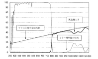
厚さ2mm、屈折率1.54の板状のガラス基体の表面にスピンコート法によって以下の条件で成膜させた。スピンコート条件としては、回転数1500rpm、回転時間90秒とし、成膜後常温常圧下で自然乾燥させた。その結果、塗膜としてのヘイズが22の実施例1の受光部を得た。この実施例1の光学特性を図11に示す。図11は縦軸を透過率、横軸を波長とした分光透過率特性のグラフである。以下図12〜図20(図14は除く)も同様である。
EXAMPLES Hereinafter, although an Example demonstrates this invention concretely, this invention is not limited to these Examples.
<Example 1>
The embodiment is a light receiving section that can be used in the first to fourth embodiments. The same applies to Examples 2 to 9 below.
(Preparation of solution for diffuse reflection layer)
An acrylic urethane resin paint (manufactured by Rock Paint Co., Ltd., product name: 088-0201 opal white) was used as the binder and fine particles constituting the layer. In the present paint, 10 to 15% by weight of titanium dioxide fine particles (particle size: about 20 nm) are dispersed. This paint was diluted with toluene to adjust the solid content to 5 to 7.5% by weight.
(Formation of diffuse reflection layer)
A film was formed on the surface of a plate-like glass substrate having a thickness of 2 mm and a refractive index of 1.54 by the spin coating method under the following conditions. As spin coating conditions, the rotation speed was 1500 rpm and the rotation time was 90 seconds. After film formation, the film was naturally dried at room temperature and normal pressure. As a result, the light-receiving part of Example 1 having a haze of 22 was obtained. The optical characteristics of Example 1 are shown in FIG. FIG. 11 is a graph of spectral transmittance characteristics with the vertical axis representing transmittance and the horizontal axis representing wavelength. The same applies to FIGS. 12 to 20 (except for FIG. 14).
<実施例2>
実施例1と同様に乱反射層用の溶液を調整し、固形分6.7〜10%となるようトルエンにて濃度希釈し調整した。得られた溶液によって上記と同様の条件のスピンコート法によって塗膜としてのヘイズが42の実施例2の受光部を得た。この実施例2の光学特性を図11に示す。
<実施例3>
実施例1と同様に乱反射層用の溶液を調整し、固形分6.7〜10%となるようトルエンにて濃度希釈し調整した。得られた溶液によって実施例2よりも若干多めの量を同様の条件のスピンコート法によって塗膜としてのヘイズが43の実施例3の受光部を得た。この実施例3の光学特性を図11に示す。
<実施例4>
実施例1と同様に乱反射層用の溶液を調整し、固形分8〜12%となるようトルエンにて濃度希釈し調整した。得られた溶液によって実施例1と同様の条件のスピンコート法によって塗膜としてのヘイズが63の実施例4の受光部を得た。この実施例4の光学特性を図11に示す。
<実施例5>
実施例1と同様に乱反射層用の溶液を調整し、固形分8〜13%となるようトルエンにて濃度希釈し調整した。得られた溶液によって実施例2よりも若干多めの量を同様の条件のスピンコート法によって塗膜としてのヘイズが65の実施例5の受光部を得た。この実施例5の光学特性を図11に示す。
<実施例6>
実施例1と同様に乱反射層用の溶液を調整し、固形分6.7〜10%となるようトルエンにて濃度希釈し調整した。得られた溶液によって実施例5よりも若干多めの量を同様の条件のスピンコート法によって塗膜としてのヘイズが82の実施例6の受光部を得た。この実施例6の光学特性を図11に示す。
<実施例7>
実施例1と同様に乱反射層用の溶液を調整し、固形分6.7〜10%となるようトルエンにて濃度希釈し調整した。得られた溶液によって実施例6よりも若干多めの量を同様の条件のスピンコート法によって塗膜としてのヘイズが95以上の実施例7の受光部を得た。この実施例7の光学特性を図11に示す。
<比較例1>
実施例1と同様に乱反射層用の溶液を調整し、固形分6.7〜10%となるようトルエンにて濃度希釈し調整した。得られた溶液によって実施例6よりも若干多めの量を同様の条件のスピンコート法によって塗膜としてのヘイズが95以上の実施例8の受光部を得た。この比較例1の光学特性を図11に示す。
<Example 2>
The solution for the irregular reflection layer was prepared in the same manner as in Example 1, and the solution was diluted with toluene so as to have a solid content of 6.7 to 10%. With the obtained solution, the light receiving part of Example 2 having a haze of 42 was obtained by spin coating under the same conditions as described above. The optical characteristics of Example 2 are shown in FIG.
<Example 3>
The solution for the irregular reflection layer was prepared in the same manner as in Example 1, and the solution was diluted with toluene so as to have a solid content of 6.7 to 10%. With the obtained solution, a light receiving part of Example 3 having a haze as a coating film of 43 was obtained by spin coating under the same conditions with a slightly larger amount than Example 2. The optical characteristics of Example 3 are shown in FIG.
<Example 4>
In the same manner as in Example 1, a solution for the irregular reflection layer was prepared, and the solution was diluted with toluene so as to have a solid content of 8 to 12%. Using the obtained solution, the light receiving part of Example 4 having a haze of 63 as a coating film was obtained by the spin coating method under the same conditions as in Example 1. The optical characteristics of Example 4 are shown in FIG.
<Example 5>
In the same manner as in Example 1, a solution for the irregular reflection layer was prepared, and the solution was diluted with toluene so as to have a solid content of 8 to 13%. With the obtained solution, a light receiving part of Example 5 having a haze of 65 as a coating film was obtained by spin coating under the same conditions with a slightly larger amount than Example 2. The optical characteristics of Example 5 are shown in FIG.
<Example 6>
The solution for the irregular reflection layer was prepared in the same manner as in Example 1, and the solution was diluted with toluene so as to have a solid content of 6.7 to 10%. With the obtained solution, a light receiving part of Example 6 having a haze of 82 as a coating film was obtained by spin coating under the same conditions with a slightly larger amount than Example 5. The optical characteristics of Example 6 are shown in FIG.
<Example 7>
The solution for the irregular reflection layer was prepared in the same manner as in Example 1, and the solution was diluted with toluene so as to have a solid content of 6.7 to 10%. Using the obtained solution, a light receiving portion of Example 7 having a haze as a coating film of 95 or more was obtained by spin coating under the same conditions with a slightly larger amount than Example 6. The optical characteristics of Example 7 are shown in FIG.
<Comparative Example 1>
The solution for the irregular reflection layer was prepared in the same manner as in Example 1, and the solution was diluted with toluene so as to have a solid content of 6.7 to 10%. With the obtained solution, a light receiving part of Example 8 having a haze as a coating film of 95 or more was obtained by spin coating under the same conditions with a slightly larger amount than Example 6. The optical characteristics of Comparative Example 1 are shown in FIG.
<実施例8>
実施例1と同様に乱反射層用の溶液を調整し、固形分6.7〜10%となるようトルエンにて濃度希釈し調整した。得られた溶液によって実施例6よりも若干多めの量を同様の条件のスピンコート法によって塗膜としてのヘイズが60の実施例8の受光部を得た。この実施例8の光学特性を図12に示す。
<実施例9>
実施例8によって成膜した白色の赤外線通信用光学物品の内面に、可視光吸収層26としての黒色の赤外線通信用光学物品(いわゆるIRブラック)を重ね合わせた。このときの光学特性を図12に示す。
<Example 8>
The solution for the irregular reflection layer was prepared in the same manner as in Example 1, and the solution was diluted with toluene so as to have a solid content of 6.7 to 10%. With the obtained solution, a light receiving part of Example 8 having a haze as a coating film of 60 was obtained by spin coating under the same conditions with a slightly larger amount than Example 6. The optical characteristics of Example 8 are shown in FIG.
<Example 9>
On the inner surface of the white infrared communication optical article formed in Example 8, a black infrared communication optical article (so-called IR black) as the visible
実施例10〜13は実施の形態3のような受光部16を想定した実施例である。
<実施例10>
1)100nmの粒径の炭酸カルシウム微粒子(白石工業社製 vigot−10)を眼鏡用に調整した眼鏡用樹脂(素材屈折率:1.6)基材中に上記微粒子を1.5重量%分散させ、紫外線吸収剤(株式会社
大和化成研究所製ダインソーブT−53)1重量%を混ぜ、板厚0.69の平板状に成型した(以下、樹脂材Aとする)。樹脂材Aの段階のヘイズは18.5であった。
2)透明板ガラスの片面にコールドミラー膜として、SiO2/TiO2 45層、逆面にAR膜としてSiO2/TiO25層をそれぞれ真空蒸着法によって成膜した(以下、ミラー材Aとする)。
3)ミラー材Aのコールドミラー膜45層側に樹脂材Aを接着剤(東レ・ダウコーニング製SYLGARD(R) 184)で貼り合せた。この実施例10の光学特性を図13に示す。
Examples 10 to 13 are examples assuming the
<Example 10>
1) Calcium carbonate fine particles having a particle diameter of 100 nm (vigot-10, manufactured by Shiroishi Kogyo Co., Ltd.) for eyeglasses (material refractive index: 1.6) 1.5% by weight of the fine particles dispersed in a base material Then, 1 wt% of an ultraviolet absorber (Dynesorb T-53 manufactured by Daiwa Kasei Laboratory Co., Ltd.) was mixed and molded into a flat plate having a thickness of 0.69 (hereinafter referred to as “resin material A”). The haze at the stage of the resin material A was 18.5.
2) A SiO 2 / TiO 2 45 layer was formed as a cold mirror film on one side of a transparent plate glass, and a SiO 2 /
3) The resin material A was bonded to the cold mirror film 45 layer side of the mirror material A with an adhesive (SYLGARD® 184 manufactured by Dow Corning Toray). The optical characteristics of Example 10 are shown in FIG.
<実施例11>
100nmの粒径の炭酸カルシウム微粒子(白石工業社製 vigot−10)を眼鏡用に調整した眼鏡用樹脂(素材屈折率:1.6)基材中に上記微粒子を1.5重量%分散させ、蛍光顔料(株式会社エポック社製:蛍光顔料ブルーl-02-001B)を0.5重量%分散させ、板厚2mmの平板状に成型した。実施例11のヘイズは81.7であった。実施例11は図14の反射特性に示すように青色付近の波長域の反射率が他の可視光に比較して大きく肉眼では青白色を呈するものである。この実施例11の光学特性を図15に示す。
<実施例12>
100nmの粒径の炭酸カルシウム微粒子(白石工業社製 vigot−10)を眼鏡用に調整した眼鏡用樹脂(素材屈折率:1.6)基材中に上記微粒子を3重量%分散させ、蛍光顔料(株式会社エポック社製:ライムl-02-001LI)を0.5重量%分散させ、板厚2mmの平板状に成型した。実施例12のヘイズは96.7であった。実施例12は図14の反射特性に示すように青色と黄色付近の波長域の反射率が他の可視光に比較して大きく肉眼では緑白色を呈するものである。この実施例12の光学特性を図15に示す。
<実施例13>
100nmの粒径の炭酸カルシウム微粒子(白石工業社製 vigot−10)を眼鏡用に調整した眼鏡用樹脂(素材屈折率:1.6)基材中に上記微粒子を3重量%分散させ、蛍光顔料(株式会社エポック社製:レッドl-02-001R)を0.5重量%分散させ、板厚2mmの平板状に成型した。実施例13のヘイズは88.2であった。実施例13は図14の反射特性に示すように青色と赤色付近の波長域の反射率が他の可視光に比較して大きく肉眼ではピンク白色を呈するものである。この実施例13の光学特性を図15に示す。
<Example 11>
Disperse the fine particles 1.5% by weight in a resin for spectacles (material refractive index: 1.6) prepared by adjusting calcium carbonate fine particles (vigot-10 manufactured by Shiraishi Kogyo Co., Ltd.) having a particle size of 100 nm for spectacles, A fluorescent pigment (manufactured by Epoch Co., Ltd .: fluorescent pigment blue I-02-001B) was dispersed by 0.5% by weight and molded into a flat plate having a thickness of 2 mm. The haze of Example 11 was 81.7. In Example 11, as shown in the reflection characteristics of FIG. 14, the reflectance in the wavelength region near blue is larger than that of other visible light, and bluish white is exhibited to the naked eye. The optical characteristics of Example 11 are shown in FIG.
<Example 12>
3% by weight of the above fine particles are dispersed in a base material for a spectacle resin (material refractive index: 1.6) in which calcium carbonate fine particles (vigot-10 manufactured by Shiraishi Kogyo Co., Ltd.) having a particle diameter of 100 nm are prepared for spectacles, and fluorescent pigment (Epoch Co., Ltd .: Lime l-02-001LI) was dispersed in an amount of 0.5% by weight and molded into a flat plate having a thickness of 2 mm. The haze of Example 12 was 96.7. In Example 12, as shown in the reflection characteristics of FIG. 14, the reflectance in the wavelength range near blue and yellow is larger than that of other visible light, and greenish white is exhibited to the naked eye. The optical characteristics of Example 12 are shown in FIG.
<Example 13>
3% by weight of the above fine particles are dispersed in a base material for a spectacle resin (material refractive index: 1.6) in which calcium carbonate fine particles (vigot-10 manufactured by Shiraishi Kogyo Co., Ltd.) having a particle diameter of 100 nm are prepared for spectacles, and fluorescent pigment 0.5% by weight (manufactured by Epoch Co., Ltd .: Red l-02-001R) was dispersed and molded into a flat plate having a thickness of 2 mm. The haze of Example 13 was 88.2. In Example 13, as shown in the reflection characteristics of FIG. 14, the reflectance in the wavelength region near blue and red is larger than that of other visible light, and pinkish white is exhibited to the naked eye. The optical characteristics of Example 13 are shown in FIG.
実施例14〜16は実施の形態10のような受光部33を想定した実施例であり、赤外線帯域として850nmの波長で12%の透過率を維持し、一方可視域の透過率を平均で5%以下に制御した例である。
<実施例14>
150nmの粒径の炭酸カルシウム微粒子(白石工業社製 vigot−15)を眼鏡用に調整した眼鏡用樹脂(素材屈折率:1.6)基材中に上記微粒子を3重量%分散させ、板厚4.4mmの平板状に成型した。ヘイズは90以上であった。この実施例14の光学特性を図16に示す。
<実施例15>
2.2μmの粒径のシリカ (トクヤマ社製 ファインシール)を眼鏡用に調整した眼鏡用樹脂(素材屈折率:1.6)基材中に上記微粒子を0.5重量%分散させ、板厚6mmの平板状に成型した。ヘイズは90以上であった。この実施例15の光学特性を図16に示す。
<実施例16>
10μmの粒径のシリカ (トクヤマ社製 トクシールU)を眼鏡用に調整した眼鏡用樹脂(素材屈折率:1.6)基材中に上記微粒子を0.7重量%分散させ、板厚3.3mmの平板状に成型した。ヘイズは90以上であった。この実施例16の光学特性を図16に示す。
尚、実施例14〜16の光学特性の比較として実施例7の樹脂材Aの特性を図16上に図示する。
Examples 14 to 16 are examples in which the
<Example 14>
3% by weight of the above-mentioned fine particles are dispersed in a base material for a spectacle resin (material refractive index: 1.6) in which calcium carbonate fine particles having a particle diameter of 150 nm (vigot-15 manufactured by Shiraishi Kogyo Co., Ltd.) are prepared for spectacles. It was molded into a 4.4 mm flat plate. The haze was 90 or more. The optical characteristics of Example 14 are shown in FIG.
<Example 15>
The above fine particles are dispersed in an amount of 0.5% by weight in a resin for spectacles (refractive index of material: 1.6) prepared by using silica having a particle size of 2.2 μm (Fine Seal manufactured by Tokuyama Co., Ltd.) for the spectacles. Molded into a 6 mm flat plate. The haze was 90 or more. The optical characteristics of Example 15 are shown in FIG.
<Example 16>
2. Disperse 0.7% by weight of the fine particles in a spectacle resin (material refractive index: 1.6) base material prepared by using silica (Tokuyama U made by Tokuyama Corporation) having a particle size of 10 μm for spectacles; Molded into a 3 mm flat plate. The haze was 90 or more. The optical characteristics of Example 16 are shown in FIG.
In addition, the characteristic of the resin material A of Example 7 is illustrated on FIG. 16 as a comparison of the optical characteristics of Examples 14-16.
<実施例17>
100nmの粒径の炭酸カルシウム微粒子(白石工業社製 vigot−10)を眼鏡用に調整した眼鏡用樹脂(素材屈折率:1.6)基材中に上記微粒子を3重量%分散させ、紫外線吸収剤(株式会社大和化成研究所製ダインソーブT−53)1重量%を混ぜ板厚1.3mmの平板状に成型した。この段階のヘイズは53.45であった。この板材を染料(日本化薬社製: Kayalon Polyster Yellow 5R−SE200)を3g/リットルの水に界面活性剤(日本乳化剤株式会社製 ニューコール210)とキャリア剤(大和化学工業社製:ダイキャリアDK−CN)を添加し、90℃に加温した中に30分浸漬して実施例17を得た。実施例17は肉眼ではオレンジ白色を呈するものである。また、比較として上記眼鏡用樹脂に実施例17と同じ条件での染料だけを分散させたもの(樹脂材Bとする)を作成した。また、比較のため実施例17において染料のみ入れていない条件で調整したものを作成した。図17に樹脂材Bの透過特性を示す。実施例17の光学特性を図18に示す。
<実施例18>
100nmの粒径の炭酸カルシウム微粒子(白石工業社製 vigot−10)を眼鏡用に調整した眼鏡用樹脂(素材屈折率:1.6)基材中に上記微粒子を3重量%分散させ、紫外線吸収剤(株式会社大和化成研究所製ダインソーブT−53)1重量%を混ぜ板厚1.3mmの平板状に成型した。この段階のヘイズは53.45であった。この板材を染料(双葉産業製 FSP BLUE AUL-S)を3g/リットルの水に界面活性剤(日本乳化剤株式会社製 ニューコール210)とキャリア剤(大和化学工業社製:ダイキャリアDK−CN)を添加し、90℃に加温した中に30分浸漬して実施例18を得た。実施例18は肉眼では青白色を呈するものである。また、比較として上記眼鏡用樹脂に実施例18と同じ条件で染料だけを分散させたものを作成した(樹脂材Cとする)。図17に樹脂材Cの透過特性を示す。実施例18の光学特性を図18に示す。
<Example 17>
3% by weight of the above-mentioned fine particles are dispersed in a base material for a spectacle resin (material refractive index: 1.6) in which calcium carbonate fine particles (Vigot-10 manufactured by Shiraishi Kogyo Co., Ltd.) having a particle diameter of 100 nm are prepared for spectacles, and absorbs ultraviolet rays. 1% by weight of an agent (Dynesorb T-53, manufactured by Daiwa Kasei Laboratories, Inc.) was mixed and molded into a flat plate shape having a thickness of 1.3 mm. The haze at this stage was 53.45. This plate material was dye (Nippon Kayaku Co., Ltd .: Kayalon Polyster Yellow 5R-SE200) in 3 g / liter of water with a surfactant (Nippon Emulsifier Co., Ltd. New Coal 210) and a carrier agent (Daiwa Chemical Industry Co., Ltd .: Die Carrier). DK-CN) was added, and the mixture was immersed in 90 ° C. for 30 minutes to obtain Example 17. Example 17 exhibits orange white color with the naked eye. For comparison, a resin (resin material B) in which only the dye under the same conditions as in Example 17 was dispersed in the above spectacle resin was prepared. Moreover, what was adjusted on the conditions which did not put only the dye in Example 17 was created for the comparison. FIG. 17 shows the transmission characteristics of the resin material B. The optical characteristics of Example 17 are shown in FIG.
<Example 18>
3% by weight of the above-mentioned fine particles are dispersed in a base material for a spectacle resin (material refractive index: 1.6) in which calcium carbonate fine particles (Vigot-10 manufactured by Shiraishi Kogyo Co., Ltd.) having a particle diameter of 100 nm are prepared for spectacles, and absorbs ultraviolet rays. 1% by weight of an agent (Dynesorb T-53, manufactured by Daiwa Kasei Laboratories, Inc.) was mixed and molded into a flat plate shape having a thickness of 1.3 mm. The haze at this stage was 53.45. Dye (FSP BLUE AUL-S made by Futaba Sangyo Co., Ltd.) was added to 3g / liter of water with a surfactant (Nippon Emulsifier Co., Ltd. New Coal 210) and a carrier agent (Daiwa Chemical Industry Co., Ltd .: Die Carrier DK-CN) Was added and immersed in 30 ° C. for 30 minutes to obtain Example 18. Example 18 is bluish white with the naked eye. For comparison, a resin in which only a dye was dispersed under the same conditions as in Example 18 was prepared (referred to as resin material C). FIG. 17 shows the transmission characteristics of the resin material C. The optical characteristics of Example 18 are shown in FIG.
<実施例19>
1)石英ガラスの片側表面をサンドブラスト用研磨剤ホワイトアランダムWA#100を用いて、圧力0.2〜0.3MPaで数十秒程度ブラスト処理した(以下、ブラスト材Aとする)。ブラスト材Aの段階のヘイズは79であった。
2)透明板ガラスの片面にコールドミラー膜として、SiO2/TiO2 49層、逆面にAR膜としてSiO2/TiO25層をそれぞれ真空蒸着法によって成膜した(以下、ミラー材Bとする)。
3)ミラー材Bのコールドミラー膜49層側に、ブラスト材をブラスト側を接着剤使用しないで重ね合わせた。この実施例19の光学特性を図19に示す。
<Example 19>
1) One side surface of quartz glass was blasted for about several tens of seconds at a pressure of 0.2 to 0.3 MPa using a sand blasting abrasive white alundum WA # 100 (hereinafter referred to as blasting material A). The haze at the stage of the blast material A was 79.
2) A SiO 2 / TiO 2 49 layer was formed as a cold mirror film on one side of the transparent plate glass, and an SiO 2 /
3) The blast material was superposed on the cold mirror film 49 layer side of the mirror material B without using an adhesive on the blast side. The optical characteristics of Example 19 are shown in FIG.
<実施例20>
1)板厚1mmのアクリル樹脂基板を100%アセトンを含ませた布で表面を軽くこすって、その後30分風乾させた(以下、アセトン処理材Aとする)。ヘイズは87であった。
2)透明板ガラスの片面にコールドミラー膜として、SiO2/TiO2 49層、逆面にSiO2/TiO25層をそれぞれ真空蒸着法によって成膜した(以下、ミラー材Cとする)。
3)ミラー材Cのコールドミラー膜49層側に、アセトン処理材Aを非処理面側を接着剤使用しないで重ね合わせた。この実施例20の光学特性を図20に示す。
<Example 20>
1) The surface of a 1 mm thick acrylic resin substrate was lightly rubbed with a cloth containing 100% acetone, and then air-dried for 30 minutes (hereinafter referred to as acetone-treated material A). The haze was 87.
2) as a cold mirror film on one side of the glazing, SiO 2 / TiO 2 49 layers was formed by a respective vacuum deposition SiO 2 /
3) The acetone-treated material A was superposed on the cold mirror film 49 layer side of the mirror material C without using an adhesive on the non-treated surface side. The optical characteristics of Example 20 are shown in FIG.
(通信性能の評価について)
市販のIrDA規格の赤外線通信方式の携帯電話を2台用意し、それぞれの赤外線ポートに同じ実施例の受光部を装着し、20cm離間させて通信可能かどうかの実験を行った。その結果、実施例1〜20については通信可能であったが、比較例1では通信できなかった。
(白色発色の評価について)
上記各実施例についてのヘイズをヘイズメーターを用いて測定し、上記のような値を得た。目視においてはいずれも十分な白濁が得られていた。
(About communication performance evaluation)
Two commercially available IrDA standard infrared communication type mobile phones were prepared, and a light receiving unit of the same example was attached to each infrared port, and an experiment was conducted to determine whether communication was possible with a distance of 20 cm. As a result, communication was possible for Examples 1 to 20, but communication was not possible in Comparative Example 1.
(About white color development)
The haze about each said Example was measured using the haze meter, and the above values were obtained. In all cases, sufficient cloudiness was obtained.
15〜18,30〜33…赤外線通信用受光部、23…赤外線通信用光学物品としての散乱反射層。
15-18, 30-33 ... Light-receiving part for infrared communication, 23 ... Scattering reflection layer as an optical article for infrared communication.
Claims (17)
2. The optical article for infrared communication according to claim 1, wherein the binder resin or the transparent base material contains one or more coloring materials that absorb a part of the visible region .
The binder resin or in the transparent substrate, and transmits infrared rays, and an optical article for infrared communication according to claim 1 or 2, characterized in that it contained a dye which absorbs part of the visible range.
The optical article for infrared communication according to any one of claims 1 to 3 , wherein an ultraviolet absorber is contained in the binder resin or the transparent substrate .
In the binder resin or in the transparent substrate, method for manufacturing an infrared communication optical article according to claim 1 4, characterized in that so as to contain a coloring material which absorbs part of the visible region one or more .
16. The optical article for infrared communication according to claim 14 or 15 , wherein the binder resin or the transparent base material contains a dye that transmits infrared rays and absorbs part of the visible range. Manufacturing method .
Priority Applications (1)
| Application Number | Priority Date | Filing Date | Title |
|---|---|---|---|
| JP2009065568A JP5358793B2 (en) | 2008-08-20 | 2009-03-18 | Optical article for infrared communication, manufacturing method thereof, and light receiving part for infrared communication |
Applications Claiming Priority (3)
| Application Number | Priority Date | Filing Date | Title |
|---|---|---|---|
| JP2008211305 | 2008-08-20 | ||
| JP2008211305 | 2008-08-20 | ||
| JP2009065568A JP5358793B2 (en) | 2008-08-20 | 2009-03-18 | Optical article for infrared communication, manufacturing method thereof, and light receiving part for infrared communication |
Related Child Applications (1)
| Application Number | Title | Priority Date | Filing Date |
|---|---|---|---|
| JP2012287035A Division JP5756962B2 (en) | 2008-08-20 | 2012-12-28 | Optical article for infrared communication and light receiving part for infrared communication |
Publications (3)
| Publication Number | Publication Date |
|---|---|
| JP2010072616A JP2010072616A (en) | 2010-04-02 |
| JP2010072616A5 JP2010072616A5 (en) | 2011-11-24 |
| JP5358793B2 true JP5358793B2 (en) | 2013-12-04 |
Family
ID=42204405
Family Applications (2)
| Application Number | Title | Priority Date | Filing Date |
|---|---|---|---|
| JP2009065568A Expired - Fee Related JP5358793B2 (en) | 2008-08-20 | 2009-03-18 | Optical article for infrared communication, manufacturing method thereof, and light receiving part for infrared communication |
| JP2012287035A Active JP5756962B2 (en) | 2008-08-20 | 2012-12-28 | Optical article for infrared communication and light receiving part for infrared communication |
Family Applications After (1)
| Application Number | Title | Priority Date | Filing Date |
|---|---|---|---|
| JP2012287035A Active JP5756962B2 (en) | 2008-08-20 | 2012-12-28 | Optical article for infrared communication and light receiving part for infrared communication |
Country Status (1)
| Country | Link |
|---|---|
| JP (2) | JP5358793B2 (en) |
Cited By (1)
| Publication number | Priority date | Publication date | Assignee | Title |
|---|---|---|---|---|
| US11814495B2 (en) | 2019-09-30 | 2023-11-14 | Toyoda Gosei Co., Ltd. | Infrared transmissive product |
Families Citing this family (36)
| Publication number | Priority date | Publication date | Assignee | Title |
|---|---|---|---|---|
| JP5286624B2 (en) * | 2009-09-04 | 2013-09-11 | 東海光学株式会社 | Method for manufacturing optical plastic article for infrared communication |
| JP2012089593A (en) * | 2010-10-18 | 2012-05-10 | Tokai Kogaku Kk | Optical article for infrared-ray communication, and light receiving unit for infrared-ray communication |
| CN107815713B (en) | 2012-06-22 | 2020-11-17 | 苹果公司 | White appearance anodized film and forming method thereof |
| JP2014071295A (en) * | 2012-09-28 | 2014-04-21 | Tokai Kogaku Kk | Optical article for infrared-ray reception/emission and infrared ray receiving/emitting part |
| JP6298605B2 (en) * | 2013-09-06 | 2018-03-20 | 旭化成株式会社 | Hard-coated polyolefin resin sheet |
| US9181629B2 (en) | 2013-10-30 | 2015-11-10 | Apple Inc. | Methods for producing white appearing metal oxide films by positioning reflective particles prior to or during anodizing processes |
| US9839974B2 (en) | 2013-11-13 | 2017-12-12 | Apple Inc. | Forming white metal oxide films by oxide structure modification or subsurface cracking |
| CN103792599A (en) * | 2014-02-28 | 2014-05-14 | 伯恩光学(惠州)有限公司 | Lens |
| CN107209304B (en) * | 2015-01-19 | 2020-06-16 | Agc株式会社 | Optical device and optical member |
| US9726791B2 (en) * | 2015-04-14 | 2017-08-08 | Face International Corporation | Systems and methods for producing objects incorporating selectably active electromagnetic energy filtering layers and coatings |
| EP3170860B1 (en) | 2015-11-19 | 2020-07-29 | 3M Innovative Properties Company | Structural adhesive with improved corrosion resistance |
| JP2019032351A (en) * | 2015-12-25 | 2019-02-28 | Agc株式会社 | Optical filter and optical device |
| WO2017124664A1 (en) | 2016-01-21 | 2017-07-27 | 3M Innovative Properties Company | Optical camouflage filters |
| JP2019507899A (en) * | 2016-01-21 | 2019-03-22 | スリーエム イノベイティブ プロパティズ カンパニー | Optical camouflage filter |
| JP2018044991A (en) * | 2016-09-12 | 2018-03-22 | 大日本印刷株式会社 | Infrared transmitting device and optical unit |
| CN109863434B (en) | 2016-10-20 | 2022-04-26 | 3M创新有限公司 | Device for optical window masking |
| JP2020507129A (en) * | 2017-01-04 | 2020-03-05 | スリーエム イノベイティブ プロパティズ カンパニー | Color compensating optical filter |
| JP7456927B2 (en) * | 2017-07-26 | 2024-03-27 | スリーエム イノベイティブ プロパティズ カンパニー | optical camouflage filter |
| JP7057487B2 (en) * | 2017-09-20 | 2022-04-20 | Agc株式会社 | Optical equipment and components |
| US10948640B2 (en) | 2018-03-13 | 2021-03-16 | Viavi Solutions Inc. | Sensor window with a set of layers configured to a particular color and associated with a threshold opacity in a visible spectral range wherein the color is a color-matched to a surface adjacent to the sensor window |
| US11009636B2 (en) * | 2018-03-13 | 2021-05-18 | Viavi Solutions Inc. | Sensor window to provide different opacity and transmissivity at different spectral ranges |
| KR20190108073A (en) * | 2018-03-13 | 2019-09-23 | 비아비 솔루션즈 아이엔씨. | Optical device including stack of optical layers with functional treatment |
| US10845508B2 (en) * | 2018-05-31 | 2020-11-24 | Microsoft Technology Licensing, Llc | Optical stack including embedded diffuse surface |
| KR102131995B1 (en) | 2018-06-29 | 2020-07-08 | 주식회사 엘지화학 | Uv-cut film |
| JP7242261B2 (en) * | 2018-11-14 | 2023-03-20 | 豊田合成株式会社 | Infrared transmission cover |
| JP2020197595A (en) * | 2019-05-31 | 2020-12-10 | リンテック株式会社 | Light diffusion control film |
| JP7044952B2 (en) * | 2020-03-16 | 2022-03-30 | 日東電工株式会社 | Optical filter, its manufacturing method and optical module |
| KR20220154705A (en) | 2020-03-16 | 2022-11-22 | 닛토덴코 가부시키가이샤 | Optical filter, its manufacturing method and optical module |
| US11914177B2 (en) | 2020-03-16 | 2024-02-27 | Nitto Denko Corporation | Optical filter, method for manufacturing same, and optical module |
| WO2021187434A1 (en) | 2020-03-16 | 2021-09-23 | 日東電工株式会社 | Optical filter, method for manufacturing same, and optical module |
| US20230228919A1 (en) * | 2020-05-08 | 2023-07-20 | 3M Innovative Properties Company | Optical Films and Stacks Including Optically Diffusive Layer |
| KR20230127202A (en) * | 2020-09-22 | 2023-08-31 | 오티아이 루미오닉스 인크. | A device that includes an IR signal transmission area |
| JPWO2023008087A1 (en) | 2021-07-30 | 2023-02-02 | ||
| WO2023074626A1 (en) * | 2021-10-28 | 2023-05-04 | 日東電工株式会社 | Optical laminate, infrared information acquisition system, and meeting support system |
| JPWO2023080016A1 (en) | 2021-11-04 | 2023-05-11 | ||
| JP7448605B1 (en) | 2022-10-05 | 2024-03-12 | 株式会社コゾフィルタース | Filter lenses and filter lenses for digital cameras |
Family Cites Families (9)
| Publication number | Priority date | Publication date | Assignee | Title |
|---|---|---|---|---|
| JPS62284303A (en) * | 1986-06-02 | 1987-12-10 | Sumitomo Chem Co Ltd | Composition for far infrared selective permeable filter |
| JPS6373203A (en) * | 1986-09-17 | 1988-04-02 | Sumitomo Bakelite Co Ltd | Particle dispersion type composite infrared band pass filter |
| JPH0443303A (en) * | 1990-06-11 | 1992-02-13 | Matsushita Electric Ind Co Ltd | Infrared optical parts |
| JPH04315927A (en) * | 1991-04-15 | 1992-11-06 | Horiba Ltd | Infrared ray detector |
| JPH0921701A (en) * | 1995-07-04 | 1997-01-21 | Sumitomo Electric Ind Ltd | Optical window material |
| JP3568493B2 (en) * | 2001-06-18 | 2004-09-22 | 日本写真印刷株式会社 | Infrared transmission cover panel, decorative sheet for infrared transmission cover panel |
| JP3900957B2 (en) * | 2002-02-15 | 2007-04-04 | 三菱電機株式会社 | Infrared camera |
| JP4122010B2 (en) * | 2004-11-12 | 2008-07-23 | 東海光学株式会社 | Infrared light emitter / receiver |
| JP2006327882A (en) * | 2005-05-27 | 2006-12-07 | Nippon Electric Glass Co Ltd | Crystallized glass, crystallized glass building material, and manufacture method of crystallized glass article |
-
2009
- 2009-03-18 JP JP2009065568A patent/JP5358793B2/en not_active Expired - Fee Related
-
2012
- 2012-12-28 JP JP2012287035A patent/JP5756962B2/en active Active
Cited By (2)
| Publication number | Priority date | Publication date | Assignee | Title |
|---|---|---|---|---|
| US11814495B2 (en) | 2019-09-30 | 2023-11-14 | Toyoda Gosei Co., Ltd. | Infrared transmissive product |
| US12071528B2 (en) | 2019-09-30 | 2024-08-27 | Toyoda Gosei Co., Ltd. | Infrared transmissive product |
Also Published As
| Publication number | Publication date |
|---|---|
| JP5756962B2 (en) | 2015-07-29 |
| JP2013065052A (en) | 2013-04-11 |
| JP2010072616A (en) | 2010-04-02 |
Similar Documents
| Publication | Publication Date | Title |
|---|---|---|
| JP5358793B2 (en) | Optical article for infrared communication, manufacturing method thereof, and light receiving part for infrared communication | |
| EP3118658B1 (en) | Mirror-coated lens | |
| JP4122010B2 (en) | Infrared light emitter / receiver | |
| JP6756743B2 (en) | Transparent heat shield and heat insulating member with transparent screen function | |
| CN106249322B (en) | It is included in the optical goods of the anti-reflection coating with low reflection in ultra-violet (UV) band and visible region | |
| KR102232170B1 (en) | Optical product, glasses lens and glasses | |
| KR101147416B1 (en) | Display device | |
| JP4970465B2 (en) | Optical diffuser with UV blocking film | |
| CN107111000B (en) | Including the optical article in ultraviolet region interference coatings with high reflectivity | |
| JP2008160115A (en) | Infrared light receiving/emitting member | |
| CN101551474A (en) | Antidazzle hard coating film, polarizing film using the film and image display apparatus | |
| EP3658517B1 (en) | Multi-layer antireflective coated articles | |
| CN102033252A (en) | Hard-coated antiglare film, polarizing plate and image display including the same | |
| JP2005316415A (en) | Antireflective laminate | |
| KR100676405B1 (en) | Reflection-reducing film | |
| KR102350314B1 (en) | Anti-reflective coated article and method of making same | |
| KR100858049B1 (en) | Low-reflection films with neutral reflective colors and high anti-scratch properties | |
| KR20190132231A (en) | Anti-reflective film, polarizing plate, and display apparatus | |
| JP6081753B2 (en) | Optical element | |
| US8778489B2 (en) | Optical layered product | |
| JP2016206682A (en) | Optical element | |
| KR102056339B1 (en) | Optical product and plastic eyeglass lens | |
| JP2000177381A (en) | Low reflecting windshield for vehicle | |
| JP2003255106A (en) | Antireflection film | |
| JP2012089593A (en) | Optical article for infrared-ray communication, and light receiving unit for infrared-ray communication |
Legal Events
| Date | Code | Title | Description |
|---|---|---|---|
| A521 | Request for written amendment filed |
Free format text: JAPANESE INTERMEDIATE CODE: A523 Effective date: 20111007 |
|
| A621 | Written request for application examination |
Free format text: JAPANESE INTERMEDIATE CODE: A621 Effective date: 20111007 |
|
| A977 | Report on retrieval |
Free format text: JAPANESE INTERMEDIATE CODE: A971007 Effective date: 20121010 |
|
| A131 | Notification of reasons for refusal |
Free format text: JAPANESE INTERMEDIATE CODE: A131 Effective date: 20121102 |
|
| A521 | Request for written amendment filed |
Free format text: JAPANESE INTERMEDIATE CODE: A523 Effective date: 20121228 |
|
| TRDD | Decision of grant or rejection written | ||
| A01 | Written decision to grant a patent or to grant a registration (utility model) |
Free format text: JAPANESE INTERMEDIATE CODE: A01 Effective date: 20130802 |
|
| A61 | First payment of annual fees (during grant procedure) |
Free format text: JAPANESE INTERMEDIATE CODE: A61 Effective date: 20130807 |
|
| R150 | Certificate of patent or registration of utility model |
Ref document number: 5358793 Country of ref document: JP Free format text: JAPANESE INTERMEDIATE CODE: R150 Free format text: JAPANESE INTERMEDIATE CODE: R150 |
|
| R250 | Receipt of annual fees |
Free format text: JAPANESE INTERMEDIATE CODE: R250 |
|
| LAPS | Cancellation because of no payment of annual fees |