EP3537184A1 - Radiographic image detection device - Google Patents
Radiographic image detection device Download PDFInfo
- Publication number
- EP3537184A1 EP3537184A1 EP19159932.3A EP19159932A EP3537184A1 EP 3537184 A1 EP3537184 A1 EP 3537184A1 EP 19159932 A EP19159932 A EP 19159932A EP 3537184 A1 EP3537184 A1 EP 3537184A1
- Authority
- EP
- European Patent Office
- Prior art keywords
- base
- rear surface
- radiographic image
- detection device
- circuit
- Prior art date
- Legal status (The legal status is an assumption and is not a legal conclusion. Google has not performed a legal analysis and makes no representation as to the accuracy of the status listed.)
- Granted
Links
Images






Classifications
-
- G—PHYSICS
- G01—MEASURING; TESTING
- G01T—MEASUREMENT OF NUCLEAR OR X-RADIATION
- G01T7/00—Details of radiation-measuring instruments
-
- G—PHYSICS
- G01—MEASURING; TESTING
- G01T—MEASUREMENT OF NUCLEAR OR X-RADIATION
- G01T1/00—Measuring X-radiation, gamma radiation, corpuscular radiation, or cosmic radiation
- G01T1/16—Measuring radiation intensity
- G01T1/24—Measuring radiation intensity with semiconductor detectors
- G01T1/247—Detector read-out circuitry
-
- A—HUMAN NECESSITIES
- A61—MEDICAL OR VETERINARY SCIENCE; HYGIENE
- A61B—DIAGNOSIS; SURGERY; IDENTIFICATION
- A61B6/00—Apparatus or devices for radiation diagnosis; Apparatus or devices for radiation diagnosis combined with radiation therapy equipment
- A61B6/42—Arrangements for detecting radiation specially adapted for radiation diagnosis
- A61B6/4208—Arrangements for detecting radiation specially adapted for radiation diagnosis characterised by using a particular type of detector
-
- A—HUMAN NECESSITIES
- A61—MEDICAL OR VETERINARY SCIENCE; HYGIENE
- A61B—DIAGNOSIS; SURGERY; IDENTIFICATION
- A61B6/00—Apparatus or devices for radiation diagnosis; Apparatus or devices for radiation diagnosis combined with radiation therapy equipment
- A61B6/42—Arrangements for detecting radiation specially adapted for radiation diagnosis
- A61B6/4208—Arrangements for detecting radiation specially adapted for radiation diagnosis characterised by using a particular type of detector
- A61B6/4233—Arrangements for detecting radiation specially adapted for radiation diagnosis characterised by using a particular type of detector using matrix detectors
-
- A—HUMAN NECESSITIES
- A61—MEDICAL OR VETERINARY SCIENCE; HYGIENE
- A61B—DIAGNOSIS; SURGERY; IDENTIFICATION
- A61B6/00—Apparatus or devices for radiation diagnosis; Apparatus or devices for radiation diagnosis combined with radiation therapy equipment
- A61B6/42—Arrangements for detecting radiation specially adapted for radiation diagnosis
- A61B6/4283—Arrangements for detecting radiation specially adapted for radiation diagnosis characterised by a detector unit being housed in a cassette
-
- A—HUMAN NECESSITIES
- A61—MEDICAL OR VETERINARY SCIENCE; HYGIENE
- A61B—DIAGNOSIS; SURGERY; IDENTIFICATION
- A61B6/00—Apparatus or devices for radiation diagnosis; Apparatus or devices for radiation diagnosis combined with radiation therapy equipment
- A61B6/50—Apparatus or devices for radiation diagnosis; Apparatus or devices for radiation diagnosis combined with radiation therapy equipment specially adapted for specific body parts; specially adapted for specific clinical applications
- A61B6/505—Apparatus or devices for radiation diagnosis; Apparatus or devices for radiation diagnosis combined with radiation therapy equipment specially adapted for specific body parts; specially adapted for specific clinical applications for diagnosis of bone
-
- G—PHYSICS
- G01—MEASURING; TESTING
- G01T—MEASUREMENT OF NUCLEAR OR X-RADIATION
- G01T1/00—Measuring X-radiation, gamma radiation, corpuscular radiation, or cosmic radiation
- G01T1/16—Measuring radiation intensity
- G01T1/161—Applications in the field of nuclear medicine, e.g. in vivo counting
-
- G—PHYSICS
- G01—MEASURING; TESTING
- G01T—MEASUREMENT OF NUCLEAR OR X-RADIATION
- G01T1/00—Measuring X-radiation, gamma radiation, corpuscular radiation, or cosmic radiation
- G01T1/16—Measuring radiation intensity
- G01T1/20—Measuring radiation intensity with scintillation detectors
- G01T1/202—Measuring radiation intensity with scintillation detectors the detector being a crystal
-
- G—PHYSICS
- G01—MEASURING; TESTING
- G01T—MEASUREMENT OF NUCLEAR OR X-RADIATION
- G01T1/00—Measuring X-radiation, gamma radiation, corpuscular radiation, or cosmic radiation
- G01T1/16—Measuring radiation intensity
- G01T1/24—Measuring radiation intensity with semiconductor detectors
- G01T1/244—Auxiliary details, e.g. casings, cooling, damping or insulation against damage by, e.g. heat, pressure or the like
-
- G—PHYSICS
- G03—PHOTOGRAPHY; CINEMATOGRAPHY; ANALOGOUS TECHNIQUES USING WAVES OTHER THAN OPTICAL WAVES; ELECTROGRAPHY; HOLOGRAPHY
- G03B—APPARATUS OR ARRANGEMENTS FOR TAKING PHOTOGRAPHS OR FOR PROJECTING OR VIEWING THEM; APPARATUS OR ARRANGEMENTS EMPLOYING ANALOGOUS TECHNIQUES USING WAVES OTHER THAN OPTICAL WAVES; ACCESSORIES THEREFOR
- G03B42/00—Obtaining records using waves other than optical waves; Visualisation of such records by using optical means
- G03B42/02—Obtaining records using waves other than optical waves; Visualisation of such records by using optical means using X-rays
Definitions
- the present invention relates to a radiographic image detection device.
- the radiographic image detection device comprises a sensor panel, a circuit unit, and a base.
- the sensor panel a plurality of pixels that accumulate charge in response to radiation which has been emitted from a radiation source and then transmitted through a subject (patient) are two-dimensionally arranged.
- the radiographic image detection device comprising the sensor panel is also called a flat panel detector (FPD).
- the circuit unit converts the charge accumulated in the pixels of the sensor panel into a digital signal and outputs the digital signal as a radiographic image.
- the circuit unit includes a plurality of circuit substrates on which various circuits are mounted.
- the base has a front surface to which the sensor panel is attached and a rear surface on which the circuit substrates are mounted.
- JP2013-200188A discloses a radiographic image detection device in which a base having a front surface to which a sensor panel is attached and a rear surface on which a circuit substrate is mounted is used as a heat insulating structure, which makes it difficult for the driving heat of the circuit substrate to be transferred to the sensor panel through the base.
- the base includes two plates and an internal portion interposed between the two plates.
- the internal portion has a honeycomb structure in which columnar spaces formed by cell walls of regular hexagonal columns are arranged without a gap therebetween.
- a thermal conduction path in the honeycomb structure is narrower than that in a solid structure. Therefore, it is possible to significantly reduce the amount of driving heat transferred to the sensor panel.
- circuit substrates generate a relatively large amount of driving heat and others generate a relatively small amount of driving heat.
- circuit substrates having different sizes or shapes and there are various layouts of the circuit substrates on the rear surface of the base. Therefore, a temperature distribution in the rear surface of the base is not uniform and the rear surface of the base has a portion that is locally heated and another portion that is not locally heated. In a case in which heat with a non-uniform temperature distribution is transferred to the sensor panel through the base and the sensor panel is locally heated, local density unevenness occurs in a radiographic image and the quality of the radiographic image is degraded.
- the base is used as the heat insulating structure and driving heat unlikely to be transferred in the thickness direction.
- the base is used as the heat insulating structure and driving heat unlikely to be transferred in the thickness direction.
- An object of the invention is to provide a radiographic image detection device that can reduce the possibility that a sensor panel will be locally heated by the driving heat of a circuit substrate and can suppress the degradation of the quality of a radiographic image.
- a radiographic image detection device comprising: a sensor panel in which pixels that accumulate charge in response to radiation, which has been emitted from a radiation source and transmitted through a subject, are two-dimensionally arranged; a circuit unit that converts the charge into a digital signal, outputs the digital signal as a radiographic image, and includes a plurality of circuit substrates on which various circuits are mounted; and a base that has a front surface to which the sensor panel is attached and a rear surface on which the circuit substrates are mounted and has anisotropic thermal conductivity in at least the rear surface.
- At least one of the plurality of circuit substrates has a rectangular shape in a plan view and is provided such that a long side direction is perpendicular to a direction in which thermal conductivity is high in the rear surface.
- a length of a long side of the circuit substrate is equal to or greater than a quarter of a length of a side of the base along the long side direction.
- the rear surface is divided into two equal regions, that is, a high-density region in which mounting density of the circuit substrates is relatively high and a low-density region in which the mounting density of the circuit substrates is relatively low and the circuit substrates are provided in the high-density region and the low-density region.
- thermal conductivity in a direction from the high-density region to the low-density region is high.
- the rear surface is divided into two equal regions, that is, a high-temperature region in which an amount of heat generated from the circuit substrates is relatively large and a low-temperature region in which the amount of heat generated from the circuit substrates is relatively small and the circuit substrates are provided in the high-temperature region and the low-temperature region.
- thermal conductivity in a direction from the high-temperature region to the low-temperature region is high.
- the base includes a pitch-based carbon fiber reinforced resin obtained by impregnating a pitch-based carbon fiber with a matrix resin.
- a pitch-based carbon fiber reinforced resin obtained by impregnating a pitch-based carbon fiber with a matrix resin.
- at least the rear surface of the base is made of the pitch-based carbon fiber reinforced resin.
- a sheet that is made of a pitch-based carbon fiber reinforced resin obtained by impregnating a pitch-based carbon fiber with a matrix resin is attached to the rear surface of the base. In these cases, preferably, fiber directions of the pitch-based carbon fibers are aligned with one direction.
- a heat insulating member is attached to the front surface of the base and the sensor panel is attached to the front surface through the heat insulating member.
- two pairs each including the sensor panel and the circuit unit are provided and the two sensor panels are sequentially arranged in a thickness direction.
- two radiographic images output from the two circuit units are used to calculate an index value related to bones.
- the base having the front surface to which the sensor panel is attached and the rear surface on which the circuit substrates of various circuits are mounted has anisotropic thermal conductivity in at least the rear surface. Therefore, it is possible to provide a radiographic image detection device that can reduce the possibility that a sensor panel is locally heated by the driving heat of a circuit substrate and can suppress the degradation of the quality of a radiographic image.
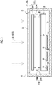
- an electronic cassette 10 corresponding to a radiographic image detection device has a first sensor panel 11A and a second sensor panel 11B which are accommodated in a housing 12.
- the first and second sensor panels 11A and 11B are thin plates having a rectangular shape in a plan view and are sequentially arranged in a thickness direction TD.
- the housing 12 is a portable box having a rectangular parallelepiped shape and has a size which is based on the International Organization for Standardization (ISO) 4090:2001 and is substantially equal to the size of, for example, a film cassette, an imaging plate (IP) cassette, or a computed radiography (CR) cassette.
- the housing 12 is made of a conductive material, such as a resin mixed with carbon fibers, a resin mixed with an aluminum or nickel filler, an aluminum alloy, or a magnesium alloy.
- the electronic cassette 10 is set in a holder 14 of an imaging table 13 on which a subject H lies supine. Then, the electronic cassette 10 receives X-rays (represented by a one-dot chain line) corresponding to radiation which has been emitted from an X-ray source 15 corresponding to a radiation source and then transmitted through the subject H and detects an X-ray image corresponding to a radiographic image.
- X-rays represented by a one-dot chain line
- the electronic cassette 10 is connected to a console 16 and communicates with the console 16 to transmit and receive various kinds of information.
- Various kinds of information include, for example, the X-ray images detected by the electronic cassette 10 and an imaging menu input by an operator through the console 16.
- the imaging menu is, for example, a set of an imaging part, such as the head or the chest, a posture, such as an upright position, a lying position, or a sitting position, and the orientation of the subject H with respect to X-rays, such as the front, the side, or the back.
- the console 16 is configured by installing a control program, such as an operating system, and various application programs in a computer such as a notebook personal computer.
- the console 16 includes a display 17 and an input device 18 such as a touch pad or a keyboard.
- the X-ray image transmitted from the electronic cassette 10 is displayed on the display 17.
- a rectangular opening is formed in a front surface of the housing 12 on which X-rays are incident and a transmission plate 25 that transmits X-rays is attached to the opening.
- the first sensor panel 11A and the second sensor panel 11B are provided immediately below the transmission plate 25.
- the thickness direction TD in which the first and second sensor panels 11A and 11B are sequentially arranged is a direction that is parallel to a line normal to the front surface of the housing 12 and a rear surface of the housing 12 opposite to the front surface.
- the first sensor panel 11A includes a first light detection substrate 26A and a first scintillator 27A.
- the first light detection substrate 26A and the first scintillator 27A are arranged in the order of the first light detection substrate 26A and the first scintillator 27A as viewed from the front surface of the housing 12 on which X-rays are incident.
- the second sensor panel 11B includes a second light detection substrate 26B and a second scintillator 27B which are arranged in the order of the second light detection substrate 26B and the second scintillator 27B as viewed from the front surface of the housing 12.
- a sensor panel in which a scintillator 27 and a light detection substrate 26 are sequentially arranged as viewed from the front surface of the housing 12 may be used.
- a direct-conversion-type sensor panel that directly converts X-rays into charge with a photoconductive film made of, for example, amorphous selenium may be used.
- the first scintillator 27A has a phosphor, such as CsI:Tl (thallium-activated cesium iodide), and the second scintillator 27B has a phosphor, such as GOS (Gd 2 O 2 S:Tb, terbium-activated gadolinium oxysulfide).
- Each of the first and second scintillators 27A and 27B converts incident X-rays into visible light and emits the visible light.
- the first and second light detection substrates 26A and 26B detect the visible light emitted from the first and second scintillators 27A and 27B and convert the visible light into charge.
- the housing 12 accommodates a base 28 in addition to the first and second sensor panels 11A and 11B.
- a heat insulating member 30 having a sheet shape is attached to a front surface (a surface on which X-rays are incident) 29 of the base 28.
- the first and second sensor panels 11A and 11B are attached to the front surface 29 of the base 28 through the heat insulating member 30.
- the heat insulating member 30 is, for example, a sponge sheet.
- three circuit substrates 32, 33, and 34 provided with various circuits are mounted and fixed to a rear surface (a surface opposite the front surface 29) 31 of the base 28 through spacers 35 that are made of metal.
- the base 28 is fixed to the inner surface of the housing 12 by, for example, a resin adhesive.
- the housing 12 accommodates a cable connector (not illustrated) that performs wired communication with the console 16 and receives power from a commercial power supply in addition to these components.
- the housing 12 may accommodate an antenna for wireless communication with the console 16 and a battery for wirelessly driving the electronic cassette 10.
- Fig. 3 which is a plan view of the base 28 as viewed from the rear surface of the housing 12, the circuit substrates 32 to 34 are arranged such that they are close to each other and are biased to one side (the upper side in Fig. 3 ) of the rear surface 31 of the base 28. All of the circuit substrates 32 to 34 have a rectangular shape in a plan view and are arranged such that the long side directions LD thereof are aligned with each other and the short side directions SD thereof are aligned with each other.
- the base 28 is made of a pitch-based carbon fiber reinforced resin 42 obtained by impregnating a pitch-based carbon fiber 40 with a matrix resin 41, as illustrated in a dashed circle.
- the pitch-based carbon fiber 40 is obtained by carbonizing a pitch precursor such as coal tar or heavy petroleum.
- the fiber directions FD of the pitch-based carbon fibers 40 are aligned with one direction. Since the pitch-based carbon fiber 40 has a higher thermal conductivity than the matrix resin 41, heat is likely to be transferred in the fiber direction FD. Therefore, in a case in which the fiber directions FD of the pitch-based carbon fibers 40 are aligned with one direction, the pitch-based carbon fiber reinforced resin 42 has a high thermal conductivity in the fiber direction FD. Since the base 28 is made of the pitch-based carbon fiber reinforced resin 42, the base 28 has anisotropic thermal conductivity. Specifically, the base 28 has high thermal conductivity in a direction DTC parallel to the fiber direction FD.
- the circuit substrates 32 to 34 are arranged such that the long side direction LD is perpendicular to the direction DTC (the short side direction SD is parallel to the direction DTC).
- the lengths L1, L2, and L3 of the long sides of the circuit substrates 32 to 34 are equal to or greater than a quarter of the length L4 of a side of the base 28 along the long side direction LD (L1, L2, and L3 ⁇ (1/4) ⁇ L4).
- the circuit substrates 32 to 34 are arranged so as to be biased to one side of the rear surface 31. Therefore, the rear surface 31 is divided into two equal regions, that is, a high-density region 45 in which the mounting density of the circuit substrates is relatively high and a low-density region 46 in which the mounting density of the circuit substrates is relatively low by a center line CL represented by a one-dot chain line. Specifically, the circuit substrates 32 and 33 and half of the circuit substrate 34 are provided in the high-density region 45 and only the other half of the circuit substrate 34 is provided in the low-density region 46.
- the high-density region 45 corresponds to a high-temperature region in which the amount of heat generated from the circuit substrates is relatively large and the low-density region 46 corresponds to a low-temperature region in which the amount of heat generated from the circuit substrates is relatively small.
- the direction DTC of the rear surface 31 in which thermal conductivity is high is a direction from the high-density and high-temperature region 45 to the low-density and low-temperature region 46. Therefore, the rear surface 31 has high thermal conductivity in the direction from the high-density region to the low-density region and has high thermal conductivity in the direction from the high-temperature region to the low-temperature region.
- the mounting density of the circuit substrates literally means the percentage of the area of the circuit substrates in each of the two equally divided regions of the rear surface 31.
- the amount of heat generated from the circuit substrates specifically means the maximum temperature of the driving heat of the circuit substrate.
- the relatively large or small amount of heat generated from the circuit substrate is the comparison result of the sum of the amounts of heat generated from the provided circuit substrates. That is, in a case in which the sum of the amounts of heat generated from the circuit substrates provided in one of the two equally divided regions of the rear surface 31 is larger than the sum of the amounts of heat generated from the circuit substrates provided in the other region, the one region is the high-temperature region and the other region is the low-temperature region.
- the one region is the high-temperature region and the other region is the low-temperature region. That is, the distinction between the high-temperature region and the low-temperature region does not depend on the number of circuit substrates provided and is determined by the sum of the amounts of heat generated from the circuit substrates provided.
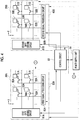
- the first light detection substrate 26A is configured by providing first pixels 50A which are arranged in a two-dimensional matrix of N rows and M columns, N first gate lines 51A, and M first signal lines 52A on a glass substrate (not illustrated).
- the first gate lines 51A extend in the X direction along a row direction of the first pixels 50A and are arranged at a predetermined pitch in the Y direction along a column direction of the first pixels 50A.
- the first signal lines 52A extend in the Y direction and are arranged at a predetermined pitch in the X direction.
- the first gate lines 51A and the first signal lines 52A are orthogonal to each other and the first pixels 50A are provided so as to correspond to the intersection points between the first gate lines 51A and the first signal lines 52A.
- N and M are integers that are equal to or greater than 2.
- N is 2880 and M is 2304.
- the array of the first pixels 50A may be a square array as illustrated in Fig. 4 .
- the first pixels 50A may be inclined at 45° and may be arranged in zigzag.
- the first pixel 50A comprises a first photoelectric conversion unit 53A on which visible light is incident and which generates charge (electron-hole pair) and accumulates the charge and a first thin film transistor (TFT) 54A.
- the first photoelectric conversion unit 53A has a structure in which an upper electrode and a lower electrode are provided on the upper and lower sides of a semiconductor layer that generates charge.
- the semiconductor layer is, for example, a p-intrinsic-n (PIN) type and includes an N-type layer provided on the upper electrode side and a P-type layer provided on the lower electrode side.
- the first TFT 54A has a gate electrode connected to the first gate line 51A, a source electrode connected to the first signal line 52A, and a drain electrode connected to the lower electrode of the first photoelectric conversion unit 53A.
- a light detection substrate that is not a TFT type, but is a complementary metal oxide semiconductor (CMOS) type may be used.
- CMOS complementary metal oxide semiconductor
- a bias line (not illustrated) is connected to the upper electrode of the first photoelectric conversion unit 53A.
- a positive bias voltage is applied to the upper electrode through the bias line.
- the positive bias voltage is applied to generate an electric field in the semiconductor layer. Therefore, in the electron-hole pair generated in the semiconductor layer by photoelectric conversion, the electron is moved to the upper electrode and is absorbed by the bias line and the hole is moved to the lower electrode and is collected as charge.
- the second light detection substrate 26B has the same configuration as the first light detection substrate 26A. Therefore, alphabet "B" is added next to numbers for components of the second light detection substrate 26B to distinguish the components from the components of the first light detection substrate 26A and the description of the components will not be repeated.
- first circuit unit 60A is for the first sensor panel 11A.
- second circuit unit 60B is for the second sensor panel 11B. That is, there are two pairs of the sensor panels and the circuit units, that is, a pair of the first sensor panel 11A and the first circuit unit 60A and a pair of the second sensor panel 11B and the second circuit unit 60B.
- the first circuit unit 60A includes a first gate driving circuit 61A, a first signal processing circuit 62A, and a control circuit 63.
- the second circuit unit 60B includes a second gate driving circuit 61B, a second signal processing circuit 62B, and the control circuit 63. That is, the control circuit 63 is shared by the first and second circuit units 60A and 60B.
- the first gate driving circuit 61A is connected to the ends of the first gate lines 51A and generates a gate pulse for driving the first TFTs 54A.
- the control circuit 63 drives the first TFTs 54A through the first gate driving circuit 61A and controls the driving of the first signal processing circuit 62A to control the operation of the first sensor panel 11A.
- control circuit 63 directs the first sensor panel 11A to perform a pixel reset operation which reads dark charge from the first pixel 50A and resets (removes) the dark charge, a pixel charge accumulation operation which accumulates charge corresponding to the amount of X-rays reaching the first pixel 50A in the first pixel 50A, and an image reading operation which reads the charge accumulated in the first pixel 50A to the first signal processing circuit 62A through the first signal line 52A.
- a pixel reset operation which reads dark charge from the first pixel 50A and resets (removes) the dark charge
- a pixel charge accumulation operation which accumulates charge corresponding to the amount of X-rays reaching the first pixel 50A in the first pixel 50A
- an image reading operation which reads the charge accumulated in the first pixel 50A to the first signal processing circuit 62A through the first signal line 52A.
- the first signal processing circuit 62A converts the accumulated charge read from the first pixel 50A by the image reading operation into an analog voltage signal. Then, the first signal processing circuit 62A performs a known correlated double sampling process for the analog voltage signal to remove a noise component from the analog voltage signal. Then, the first signal processing circuit 62A converts the analog voltage signal into a digital signal corresponding to the voltage value of the analog voltage signal (analog/digital conversion) and outputs the digital signal to the control circuit 63.
- the control circuit 63 stores the digital signal output from the first signal processing circuit 62A as an X-ray image (a first X-ray image, see Fig. 5 ) in an embedded memory (not illustrated).
- the second circuit unit 60B has the same configuration as the first circuit unit 60A. Therefore, as in the case of the second light detection substrate 26B, the description of the second circuit unit 60B is omitted.
- a power supply unit 64 supplies power to the first and second sensor panels 11A and 11B and the first and second circuit units 60A and 60B under the control of the control circuit 63.
- the power supply unit 64 is provided with a switching power supply.
- the switching power supply converts a voltage based on power from a battery or a commercial power supply into a voltage suitable for the first and second sensor panels 11A and 11B and the first and second circuit units 60A and 60B using a pulse modulation method, for example, a pulse width modulation (PWM) method, and outputs the voltage.
- PWM pulse width modulation
- the console 16 receives a first X-ray image from the first sensor panel 11A and receives a second X-ray image from the second sensor panel 11B.
- the first X-ray image and the second X-ray image are based on the charge accumulated in the first and second pixels 50A and 50B in response to the X-rays which have been emitted from the X-ray source 15 and then transmitted through the subject H, respectively, and indicate the internal structure of the body of the subject H.
- An offset correction process which removes artifacts caused by fixed pattern noise which is an example of noise caused by the usage environment of the electronic cassette 10, such as environmental temperature, is performed for the first X-ray image and the second X-ray image and then the first X-ray image and the second X-ray image are input to an ES image generation unit 70.
- the ES image generation unit 70 generates an ES image from the first X-ray image and the second X-ray image. Specifically, the ES image generation unit 70 subtracts an image obtained by multiplying the first X-ray image by a predetermined coefficient from an image obtained by multiplying the second X-ray image by a predetermined coefficient in units of pixels.
- the ES image generated by the subtraction process is, for example, an image in which soft tissues have been removed and bone tissues have been highlighted.
- a bone density calculation unit 71 calculates bone density in an imaging part of the subject H as an index value related to bones. Specifically, first, the bone density calculation unit 71 analyzes the ES image from the ES image generation unit 70 to extract a bone tissue region of the ES image. Then, for example, the bone density calculation unit 71 multiplies a representative value (for example, the mean, maximum value, or mode) of the pixel values of the bone tissue region by a conversion coefficient for converting the pixel values into a bone mass to calculate the bone mass. The bone density calculation unit 71 divides the calculated bone mass by the area of the bone tissue region to calculate bone density.
- a representative value for example, the mean, maximum value, or mode
- the console 16 displays, for example, the bone density calculated by the bone density calculation unit 71 and the ES image generated by the ES image generation unit 70 on the display 17.
- the X-ray images output from the first and second sensor panels 11A and 11B are used to calculate the index value related to bones.
- the bone mass may be displayed on the display 17.
- an application program related to X-ray imaging is executed to construct the ES image generation unit 70 and the bone density calculation unit 71 in a central processing unit (CPU) of the console 16.
- CPU central processing unit
- Some or all of the above-mentioned units may be constructed in the CPU of the electronic cassette 10 and the electronic cassette 10 may perform the generation of the ES image or the calculation of bone density.
- the operator turns on the electronic cassette 10 and sets the electronic cassette 10 in the holder 14 of the imaging table 13. Then, the operator adjusts the positional relationship among the electronic cassette 10, the X-ray source 15, and the subject H and then operates the X-ray source 15 to emit X-rays.
- the X-rays which have been emitted from the X-ray source 15 and then transmitted through the subject H are incident on the first sensor panel 11A and the second sensor panel 11B through the transmission plate 25.
- Each of the first and second sensor panels 11A and 11B receives the emitted X-rays and sequentially performs the pixel reset operation and the pixel charge accumulation operation.
- the charge corresponding to the amount of X-rays reaching each of the first and second pixels 50A and 50B is accumulated in each of the first and second pixels 50A and 50B.
- the image reading operation is performed in each of the first and second sensor panels 11A and 11B. Then, the first X-ray image and the second X-ray image are output from the first sensor panel 11A and the second sensor panel 11B, respectively.
- the circuit substrates 32 to 34 included in the first and second circuit units 60A and 60B generate heat.
- the driving heat of the circuit substrates 32 to 34 is transferred to the rear surface 31 of the base 28 on which the circuit substrates 32 to 34 are mounted through the spacers 35.
- the base 28 is made of the pitch-based carbon fiber reinforced resin 42 obtained by impregnating the pitch-based carbon fiber 40 with the matrix resin 41, the fiber directions FD of the pitch-based carbon fibers 40 are aligned with one direction, and thermal conductivity in the direction DTC parallel to the fiber direction FD is high. Therefore, the driving heat of the circuit substrates 32 to 34 transferred to the rear surface 31 of the base 28 is rapidly diffused to the entire rear surface 31 along the direction DTC and the rear surface 31 of the base 28 immediately changes to a thermal equilibrium state.
- circuit substrates 32 to 34 having a rectangular shape in a plan view are arranged such that the long side directions LD thereof are perpendicular to the direction DTC. Therefore, a large amount of driving heat of the circuit substrates 32 to 34 can be diffused not from a narrow short side but from a wide long side and it is possible to increase the speed at which the rear surface 31 of the base 28 changes to the thermal equilibrium state.
- the lengths L1, L2, and L3 of the long sides of the circuit substrates 32 to 34 are equal to or greater than a quarter of the length L4 of the side of the base 28 along the long side direction LD. Therefore, it is possible to diffuse the driving heat of the circuit substrates 32 to 34 to a wider region and to effectively prevent each of the first and second sensor panels 11A and 11B from being locally heated.
- the lengths L1, L2, and L3 of the long sides of the circuit substrates 32 to 34 are less than a quarter of the length L4 of the side of the base 28 along the long side direction LD
- the effect of diffusing the driving heat of the circuit substrates 32 to 34 is limited by anisotropy imparted to the thermal conductivity of the rear surface 31.
- the lengths of the long sides of the circuit substrates are equal to or greater than half of the side of the base 28 along the long side direction LD.
- the rear surface 31 is divided into two equal regions, that is, the high-density and high-temperature region 45 in which the amount of heat generated from the circuit substrates is relatively large and the mounting density of the circuit substrates is relatively high and the low-density and low-temperature region 46 in which the amount of heat generated from the circuit substrates is relatively small and the mounting density of the circuit substrates is relatively low.
- thermal conductivity in the direction from the high-density and high-temperature region 45 to the low-density and low-temperature region 46 is high. Therefore, it is possible to effectively diffuse driving heat from the high-density and high-temperature region 45 to the low-density and low-temperature region 46 and to further increase the speed at which the rear surface 31 of the base 28 changes to the thermal equilibrium state.
- the heat insulating member 30 is attached to the front surface 29 of the base 28 and the first and second sensor panels 11A and 11B are attached to the front surface 29 of the base 28 through the heat insulating member 30. Therefore, it is possible to effectively prevent the driving heat of the circuit substrates 32 to 34 transferred to the rear surface 31 of the base 28 from being transferred to each of the first and second sensor panels 11A and 11B.
- the first and second light detection substrates 26A and 26B and the first and second scintillators 27A and 27B are arranged in this order, respectively, as viewed from the front surface of the housing 12 on which X-rays are incident. Therefore, the driving heat of the circuit substrates 32 to 34 is less likely to be transferred to the first and second light detection substrates 26A and 26B than that in a case in which the first and second scintillators 27A and 27B and the first and second light detection substrates 26A and 26B are arranged in this order.
- Each X-ray image is transmitted from the electronic cassette 10 to the console 16.
- the ES image generation unit 70 generates an ES image and the bone density calculation unit 71 calculates bone density on the basis of the ES image.
- the bone density is displayed on the display 17 together with, for example, the ES image.
- the quality of the X-ray image which is the origin of the calculation of the index value related to bones, such as bone density is not guaranteed, there is a concern that the reliability of the index value will be significantly reduced.
- the quality of the X-ray image is guaranteed at a relatively high level, it is possible to improve the reliability of the index value.
- the amount of radiation reaching the second sensor panel 11B is reduced to 10% to 20% of the amount of radiation reaching the first sensor panel 11A. Therefore, the signal-noise (SN) ratio of the second X-ray image is reduced.
- the second sensor panel 11B is locally heated by the driving heat of the circuit substrates 32 to 34 and local density unevenness occurs in the second X-ray image, the influence of the driving heat is relatively large. Therefore, the invention is effective in the configuration in which the first and second sensor panels 11A and 11B are sequentially arranged in the thickness direction.
- the entire base 28 is not necessarily made of the pitch-based carbon fiber reinforced resin 42.
- the base 28 may include the pitch-based carbon fiber reinforced resin 42.
- at least the rear surface 31 of the base 28 may be made of the pitch-based carbon fiber reinforced resin 42.
- An electronic cassette 80 according to a second embodiment illustrated in Fig. 6 is the same as the electronic cassette 10 according to the first embodiment illustrated in Fig. 2 in, for example, the configuration of the first and second sensor panels 11A and 11B and the structure in which the first and second sensor panels 11A and 11B are attached to a front surface 82 of a base 81 through the heat insulating member 30.
- the electronic cassette 80 differs from the electronic cassette 10 in that a sheet 84 is attached to a rear surface 83 of the base 81.
- the base 81 is not made of the same pitch-based carbon fiber reinforced resin as that forming the base 28 according to the first embodiment and is made of, for example, stainless steel.
- the sheet 84 is made of a pitch-based carbon fiber reinforced resin obtained by impregnating a pitch-based carbon fiber with a matrix resin, similarly to the base 28 according to the first embodiment.
- the fiber directions FD of the pitch-based carbon fibers in the sheet 84 are aligned with one direction, which is not illustrated in the drawings.
- the circuit substrates 32 to 34 are arranged such that the long side directions LD thereof are perpendicular to the direction DTC which is parallel to the fiber direction FD and in which thermal conductivity is high. Further, thermal conductivity increases in a direction from a high-density region to a low-density region or from a high-temperature region to a low-temperature region.
- the base may not be made of the pitch-based carbon fiber reinforced resin and the sheet made of the pitch-based carbon fiber reinforced resin may be attached to the rear surface of the base to impart anisotropy to thermal conductivity in at least the rear surface of the base as in the base 81 according to this embodiment.
- the fiber directions FD of the pitch-based carbon fibers are aligned with each other to impart anisotropy to the thermal conductivity of the base.
- Anisotropy may be imparted to the thermal conductivity of the base by the following methods illustrated in, for example, Figs. 7 to 10 .
- a plurality of grooves 92 are formed in a stripe shape in a rear surface 91. Since the grooves 92 cut off a thermal conduction path in a direction perpendicular to the direction in which the grooves 92 extend, heat is unlikely to be transferred. In contrast, since a portion 93 between adjacent grooves 92 functions as the thermal conduction path in the direction DTC parallel to the direction in which the grooves 92 extend, heat is likely to be transferred. That is, in the base 90, thermal conductivity in the direction DTC is increased by the grooves 92 and anisotropy is imparted to thermal conductivity.
- a base 100 illustrated in Fig. 8 has a one-dimensional lattice shape in which a plurality of slits 103 that have the same width and pass through the base 100 from a front surface 101 to a rear surface 102 are formed at equal intervals.
- the slits 103 cut off a thermal conduction path in a direction perpendicular to the direction in which the slits 103 extend, heat is unlikely to be transferred.
- a joint portion 104 between adjacent slits 103 functions as the thermal conduction path in the direction DTC parallel to the direction in which the slits 103 extend, heat is likely to be transferred. That is, in the base 100, thermal conductivity in the direction DTC is increased by the slits 103 and anisotropy is imparted to thermal conductivity.
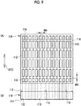
- a base 110 illustrated in Fig. 9 has a two-dimensional lattice shape (mesh shape), as compared to the base 100 having the one-dimensional lattice shape illustrated in Fig. 8 .
- Slits 113 are the same as the slits 103 illustrated in Fig. 8 in that they pass through the base 100 from a front surface 111 to a rear surface 112, have the same width, and are formed at equal intervals.
- the slit 113 is cut in the direction DTC by a joint portion 114 along a direction perpendicular to the direction DTC parallel to the direction in which the slits 113 extend.
- the slit 113 is divided into six equal parts in the direction DTC by five joint portions 114.
- the number of joint portions 114 is smaller than 14 which is the number of joint portions 115 between adjacent slits 113 counted along a direction perpendicular to the direction DTC.
- the widths WV and WH of the joint portions 114 and 115 are equal to each other.
- thermal conductivity in the direction DTC is high and anisotropy is imparted to thermal conductivity.
- the mechanical strength of the base 110 is higher than that of the base 100 illustrated in Fig. 8 .
- the width WH of the joint portion 115 may be greater than the width WV of the joint portion 114.
- a joint portion 122 between adjacent slits 121 along the direction DTC may be made of a material having a higher thermal conductivity than materials forming other portions.
- the joint portion 122 is made of copper and the other portions are made of stainless steel. In this case, it is possible to further increase thermal conductivity in the direction DTC.
- the circuit substrates are provided such that the long side directions LD thereof are perpendicular to the direction DTC, which is not illustrated in the drawings.
- thermal conductivity increases in the direction from a high-density region to a low-density region or from a high-temperature region to a low-temperature region.
- the direction DTC in which thermal conductivity is high may be changed in each region of the rear surface of the base.
- the direction DTC in which thermal conductivity is high may be inclined with respect to the side of the base.
- the base 130 is formed by bonding three blocks 130A, 130B, and 130C having a triangular shape in a plan view.
- the block 130A is provided in a central portion of the base 130 and the blocks 130B and 130C are symmetrically provided on the left and right sides of the block 130A.
- Circuit substrates 131, 132, and 133 are provided such that they are biased to one side (the upper side in Fig. 11 ) of a rear surface 134 and are close to each other.
- the circuit substrate 131 is provided over the blocks 130A to 130C.
- the circuit substrate 132 is provided in the block 130B and the circuit substrate 133 is provided in the block 130C.
- the rear surface 134 of the base 130 is divided into two equal regions, that is, a high-density and high-temperature region 135 and a low-density and low-temperature region 136 by a center line CL represented by a one-dot chain line as in the first embodiment.
- a direction DTCA in which thermal conductivity is high is parallel to the side of the base 130.
- directions DTCB and DTCC in which thermal conductivity is high are inclined with respect to the side of the base 130.
- the directions DTCB and DTCC are directions from the high-density and high-temperature region 135 to the low-density and low-temperature region 136 and are inclined outward.
- the fiber directions FDA, FDB, and FDC of pitch-based carbon fibers 40 are changed as illustrated in dashed circles such that the directions DTCA, DTCB, and DTCC in which thermal conductivity is high are different from each other.
- the direction DTC in which thermal conductivity is high may be changed in each region of the rear surface of the base or may be inclined with respect to the side of the base.
- the directions DTCB and DTCC in which thermal conductivity is high in the blocks 130B and 130C are inclined with respect to the side of the substrate and there is no difference in the direction from the high-density and high-temperature region 135 to the low-density and low-temperature region 136. Therefore, in the rear surface 134, thermal conductivity is high in the direction from the high-density region to the low-density region and is high in the direction from the high-temperature region to the low-temperature region.
- the direction DTC in which thermal conductivity is high may be changed in each region of the rear surface of the base or the direction DTC in which thermal conductivity is high may be inclined with respect to the side of the base by, for example, changing the attachment direction of the sheet 84 made of the pitch-based carbon fiber reinforced resin, by changing the extension direction of the grooves 92 illustrated in Fig. 7 , or by changing the extension direction of the slits 103, 113, and 121 illustrated in Figs. 8 to 10 in the second embodiment.
- a rear surface 141 may be divided into a plurality of regions 142, 143, and 144 and thermal conductivity in each of the regions 142 to 144 may be changed.
- the density of the pitch-based carbon fibers 40 in each of the regions 142 to 144 is changed to change thermal conductivity in each of the regions 142 to 144.
- the density of the pitch-based carbon fibers 40 in the center region 142 is higher than that in the left and right regions 143 and 144. Therefore, the thermal conductivity of the region 142 is higher than the thermal conductivity of the regions 143 and 144.
- circuit substrate 145 that generates a relatively large amount of heat is provided in the region 142 with high thermal conductivity and circuit substrates 146 and 147 that generate a relatively small amount of heat are provided in the regions 143 and 144 with low thermal conductivity. Therefore, it is possible to more actively diffuse the driving heat of the circuit substrate 145 that generates a relatively large amount of heat.
- Fig. 12 illustrates an example in which the base 140 is made of the pitch-based carbon fiber reinforced resin 42.
- the invention may be applied to the sheet 84 made of a pitch-based carbon fiber reinforced resin in the second embodiment.
- the invention may be applied to the grooves 92 illustrated in Fig. 7 .
- the number of grooves 92 in a region in which thermal conductivity is desired to increase is less than that in a region in which thermal conductivity is desired to decrease.
- the width of the portion 93 between adjacent grooves 92 in the region in which thermal conductivity is desired to increase is greater than that in the region in which thermal conductivity is desired to decrease.
- the invention may be applied to the slits 103, 113, and 121 illustrated in Figs. 8 to 10 .
- the number of joint portions 104, 115, and 122 in the region in which thermal conductivity is desired to increase is greater than that in the region in which thermal conductivity is desired to decrease.
- the width of adjacent joint portions 104, 115, and 122 in the region in which thermal conductivity is desired to increase is greater than that in the region in which thermal conductivity is desired to decrease.
- All of the circuit substrates may not be provided such that the long side directions LD thereof are perpendicular to the direction DTC.
- the circuit substrate that is provided such that the long side direction LD thereof is perpendicular to the direction DTC may be, for example, only a circuit substrate having a long side whose length is equal to or greater than a quarter of the side of the base along the long side direction or only a circuit substrate that at least generates the largest amount of heat among all of the circuit substrates.
- the center line demarcating the high-density region and the low-density region is aligned with the center line demarcating the high-temperature region and the low-temperature region.
- the center line demarcating the high-density region and the low-density region is perpendicular to the center line demarcating the high-temperature region and the low-temperature region, depending on the layout of the circuit substrates.
- the direction DTC in which thermal conductivity is high is the direction from the high-temperature region to the low-temperature region.
- the circuit substrate mounted on the rear surface of the base is not limited to a rectangular shape in a plan view.
- the circuit substrate may have a square shape in a plan view or may have a polygonal shape, a circular shape, or an elliptical shape in a plan view.
- the terms “rectangular shape” “square shape”, “polygonal shape”, “circular shape”, and “elliptic shape”, indicate that the overall contour of the circuit substrate follows the shapes. Therefore, the shapes include a case in which a circuit substrate is partially removed, such as a case in which four corners of a circuit substrate having a rectangular outline as a whole are chamfered or a case in which a central portion of a circular circuit substrate is hollowed out.
- the state in which "two sensor panels are sequentially arranged in the thickness direction” is not limited to the state in which two sensor panels are closely arranged as in each of the above-described embodiments.
- the state in which "two sensor panels are sequentially arranged in the thickness direction” also includes a state in which two sensor panels are not closely arranged and are separated from each other with a gap therebetween and a state in which an insert, such as an X-ray filter for restricting the incidence of soft ray components of X-rays, is interposed between two sensor panels.
- the electronic cassette in which two sensor panels 11A and 11B are sequentially arranged in the thickness direction TD is given as an example.
- the invention is not limited thereto.
- the invention can also be applied to an electronic cassette including one sensor panel.
- the electronic cassette is given as an example of the radiographic image detection device.
- the invention is not limited thereto.
- the invention can also be applied to a stationary radiographic image detection device that is fixed to the imaging table.
- the invention is not limited to X-rays and can also be applied to a case in which other types of radiation, such as ⁇ -rays, are used.
Landscapes
- Health & Medical Sciences (AREA)
- Life Sciences & Earth Sciences (AREA)
- Physics & Mathematics (AREA)
- Molecular Biology (AREA)
- High Energy & Nuclear Physics (AREA)
- Engineering & Computer Science (AREA)
- Medical Informatics (AREA)
- General Physics & Mathematics (AREA)
- Spectroscopy & Molecular Physics (AREA)
- Biomedical Technology (AREA)
- Optics & Photonics (AREA)
- Nuclear Medicine, Radiotherapy & Molecular Imaging (AREA)
- General Health & Medical Sciences (AREA)
- Public Health (AREA)
- Animal Behavior & Ethology (AREA)
- Biophysics (AREA)
- Pathology (AREA)
- Radiology & Medical Imaging (AREA)
- Heart & Thoracic Surgery (AREA)
- Surgery (AREA)
- Veterinary Medicine (AREA)
- Orthopedic Medicine & Surgery (AREA)
- Dentistry (AREA)
- Oral & Maxillofacial Surgery (AREA)
- Mathematical Physics (AREA)
- Chemical & Material Sciences (AREA)
- Crystallography & Structural Chemistry (AREA)
- Measurement Of Radiation (AREA)
- Apparatus For Radiation Diagnosis (AREA)
Abstract
Description
- The present invention relates to a radiographic image detection device.
- In a medical field, a diagnosis is made on the basis of a radiographic image detected by a radiographic image detection device. The radiographic image detection device comprises a sensor panel, a circuit unit, and a base. In the sensor panel, a plurality of pixels that accumulate charge in response to radiation which has been emitted from a radiation source and then transmitted through a subject (patient) are two-dimensionally arranged. The radiographic image detection device comprising the sensor panel is also called a flat panel detector (FPD). The circuit unit converts the charge accumulated in the pixels of the sensor panel into a digital signal and outputs the digital signal as a radiographic image. The circuit unit includes a plurality of circuit substrates on which various circuits are mounted. The base has a front surface to which the sensor panel is attached and a rear surface on which the circuit substrates are mounted.
- Heat is generated from a circuit substrate by the driving of various circuits.
JP2013-200188A - Some circuit substrates generate a relatively large amount of driving heat and others generate a relatively small amount of driving heat. In addition, there are various circuit substrates having different sizes or shapes and there are various layouts of the circuit substrates on the rear surface of the base. Therefore, a temperature distribution in the rear surface of the base is not uniform and the rear surface of the base has a portion that is locally heated and another portion that is not locally heated. In a case in which heat with a non-uniform temperature distribution is transferred to the sensor panel through the base and the sensor panel is locally heated, local density unevenness occurs in a radiographic image and the quality of the radiographic image is degraded.
- In
JP2013-200188A - An object of the invention is to provide a radiographic image detection device that can reduce the possibility that a sensor panel will be locally heated by the driving heat of a circuit substrate and can suppress the degradation of the quality of a radiographic image.
- In order to solve the problems, according to the invention, there is provided a radiographic image detection device comprising: a sensor panel in which pixels that accumulate charge in response to radiation, which has been emitted from a radiation source and transmitted through a subject, are two-dimensionally arranged; a circuit unit that converts the charge into a digital signal, outputs the digital signal as a radiographic image, and includes a plurality of circuit substrates on which various circuits are mounted; and a base that has a front surface to which the sensor panel is attached and a rear surface on which the circuit substrates are mounted and has anisotropic thermal conductivity in at least the rear surface.
- Preferably, at least one of the plurality of circuit substrates has a rectangular shape in a plan view and is provided such that a long side direction is perpendicular to a direction in which thermal conductivity is high in the rear surface. In this case, preferably, a length of a long side of the circuit substrate is equal to or greater than a quarter of a length of a side of the base along the long side direction.
- Preferably, the rear surface is divided into two equal regions, that is, a high-density region in which mounting density of the circuit substrates is relatively high and a low-density region in which the mounting density of the circuit substrates is relatively low and the circuit substrates are provided in the high-density region and the low-density region. Preferably, in the rear surface, thermal conductivity in a direction from the high-density region to the low-density region is high.
- Preferably, the rear surface is divided into two equal regions, that is, a high-temperature region in which an amount of heat generated from the circuit substrates is relatively large and a low-temperature region in which the amount of heat generated from the circuit substrates is relatively small and the circuit substrates are provided in the high-temperature region and the low-temperature region. Preferably, in the rear surface, thermal conductivity in a direction from the high-temperature region to the low-temperature region is high.
- Preferably, the base includes a pitch-based carbon fiber reinforced resin obtained by impregnating a pitch-based carbon fiber with a matrix resin. Preferably, at least the rear surface of the base is made of the pitch-based carbon fiber reinforced resin. Alternatively, preferably, a sheet that is made of a pitch-based carbon fiber reinforced resin obtained by impregnating a pitch-based carbon fiber with a matrix resin is attached to the rear surface of the base. In these cases, preferably, fiber directions of the pitch-based carbon fibers are aligned with one direction.
- Preferably, a heat insulating member is attached to the front surface of the base and the sensor panel is attached to the front surface through the heat insulating member.
- Preferably, two pairs each including the sensor panel and the circuit unit are provided and the two sensor panels are sequentially arranged in a thickness direction. In this case, preferably, two radiographic images output from the two circuit units are used to calculate an index value related to bones.
- According to the invention, the base having the front surface to which the sensor panel is attached and the rear surface on which the circuit substrates of various circuits are mounted has anisotropic thermal conductivity in at least the rear surface. Therefore, it is possible to provide a radiographic image detection device that can reduce the possibility that a sensor panel is locally heated by the driving heat of a circuit substrate and can suppress the degradation of the quality of a radiographic image.
-
-
Fig. 1 is a diagram illustrating an aspect of X-ray imaging. -
Fig. 2 is a diagram illustrating the internal structure of an electronic cassette. -
Fig. 3 is a plan view illustrating a base as viewed from a rear surface of a housing. -
Fig. 4 is a block diagram illustrating the electrical configuration of the electronic cassette. -
Fig. 5 is a block diagram illustrating the configuration of a console related to the calculation of bone density. -
Fig. 6 is a diagram illustrating the internal structure of an electronic cassette according to a second embodiment. -
Fig. 7 is a diagram illustrating an example in which grooves are formed in a rear surface of a base and anisotropy is imparted to the thermal conductivity of the base. (A) ofFig. 7 is a plan view illustrating the rear surface of the base and (B) ofFig. 7 is a side view illustrating the base. -
Fig. 8 is a diagram illustrating an example in which slits are formed in a base and anisotropy is imparted to the thermal conductivity of the base. (A) ofFig. 8 is a plan view illustrating the rear surface of the base and (B) ofFig. 8 is a side view illustrating the base. -
Fig. 9 is a diagram illustrating another example in which slits are formed in a base and anisotropy is imparted to the thermal conductivity of the base. (A) ofFig. 9 is a plan view illustrating the rear surface of the base and (B) ofFig. 9 is a side view illustrating the base. -
Fig. 10 is a diagram illustrating still another example in which slits are formed in a base and anisotropy is imparted to the thermal conductivity of the base. (A) ofFig. 10 is a plan view illustrating the rear surface of the base and (B) ofFig. 10 is a side view illustrating the base. -
Fig. 11 is a diagram illustrating an example in which a direction in which thermal conductivity is high is changed in each region of the rear surface and is inclined with respect to the side of the base. -
Fig. 12 is a diagram illustrating an example in which thermal conductivity is changed in each region of the rear surface of the base. - In
Fig. 1 , anelectronic cassette 10 corresponding to a radiographic image detection device according to the invention has afirst sensor panel 11A and asecond sensor panel 11B which are accommodated in ahousing 12. The first andsecond sensor panels - The
housing 12 is a portable box having a rectangular parallelepiped shape and has a size which is based on the International Organization for Standardization (ISO) 4090:2001 and is substantially equal to the size of, for example, a film cassette, an imaging plate (IP) cassette, or a computed radiography (CR) cassette. Thehousing 12 is made of a conductive material, such as a resin mixed with carbon fibers, a resin mixed with an aluminum or nickel filler, an aluminum alloy, or a magnesium alloy. - The
electronic cassette 10 is set in aholder 14 of an imaging table 13 on which a subject H lies supine. Then, theelectronic cassette 10 receives X-rays (represented by a one-dot chain line) corresponding to radiation which has been emitted from anX-ray source 15 corresponding to a radiation source and then transmitted through the subject H and detects an X-ray image corresponding to a radiographic image. - The
electronic cassette 10 is connected to aconsole 16 and communicates with theconsole 16 to transmit and receive various kinds of information. Various kinds of information include, for example, the X-ray images detected by theelectronic cassette 10 and an imaging menu input by an operator through theconsole 16. The imaging menu is, for example, a set of an imaging part, such as the head or the chest, a posture, such as an upright position, a lying position, or a sitting position, and the orientation of the subject H with respect to X-rays, such as the front, the side, or the back. - For example, the
console 16 is configured by installing a control program, such as an operating system, and various application programs in a computer such as a notebook personal computer. Theconsole 16 includes adisplay 17 and aninput device 18 such as a touch pad or a keyboard. For example, the X-ray image transmitted from theelectronic cassette 10 is displayed on thedisplay 17. - In
Fig. 2 , a rectangular opening is formed in a front surface of thehousing 12 on which X-rays are incident and atransmission plate 25 that transmits X-rays is attached to the opening. Thefirst sensor panel 11A and thesecond sensor panel 11B are provided immediately below thetransmission plate 25. Here, the thickness direction TD in which the first andsecond sensor panels housing 12 and a rear surface of thehousing 12 opposite to the front surface. Thefirst sensor panel 11A includes a firstlight detection substrate 26A and afirst scintillator 27A. The firstlight detection substrate 26A and thefirst scintillator 27A are arranged in the order of the firstlight detection substrate 26A and thefirst scintillator 27A as viewed from the front surface of thehousing 12 on which X-rays are incident. Similarly, thesecond sensor panel 11B includes a secondlight detection substrate 26B and asecond scintillator 27B which are arranged in the order of the secondlight detection substrate 26B and thesecond scintillator 27B as viewed from the front surface of thehousing 12. In addition, a sensor panel in which a scintillator 27 and a light detection substrate 26 are sequentially arranged as viewed from the front surface of thehousing 12 may be used. Further, a direct-conversion-type sensor panel that directly converts X-rays into charge with a photoconductive film made of, for example, amorphous selenium may be used. - The
first scintillator 27A has a phosphor, such as CsI:Tl (thallium-activated cesium iodide), and thesecond scintillator 27B has a phosphor, such as GOS (Gd2O2S:Tb, terbium-activated gadolinium oxysulfide). Each of the first andsecond scintillators light detection substrates second scintillators - The
housing 12 accommodates a base 28 in addition to the first andsecond sensor panels heat insulating member 30 having a sheet shape is attached to a front surface (a surface on which X-rays are incident) 29 of thebase 28. The first andsecond sensor panels front surface 29 of the base 28 through theheat insulating member 30. Theheat insulating member 30 is, for example, a sponge sheet. In contrast, threecircuit substrates spacers 35 that are made of metal. - The
base 28 is fixed to the inner surface of thehousing 12 by, for example, a resin adhesive. Thehousing 12 accommodates a cable connector (not illustrated) that performs wired communication with theconsole 16 and receives power from a commercial power supply in addition to these components. Thehousing 12 may accommodate an antenna for wireless communication with theconsole 16 and a battery for wirelessly driving theelectronic cassette 10. - In
Fig. 3 which is a plan view of the base 28 as viewed from the rear surface of thehousing 12, thecircuit substrates 32 to 34 are arranged such that they are close to each other and are biased to one side (the upper side inFig. 3 ) of therear surface 31 of thebase 28. All of thecircuit substrates 32 to 34 have a rectangular shape in a plan view and are arranged such that the long side directions LD thereof are aligned with each other and the short side directions SD thereof are aligned with each other. - The
base 28 is made of a pitch-based carbon fiber reinforcedresin 42 obtained by impregnating a pitch-basedcarbon fiber 40 with amatrix resin 41, as illustrated in a dashed circle. As is well known, the pitch-basedcarbon fiber 40 is obtained by carbonizing a pitch precursor such as coal tar or heavy petroleum. - The fiber directions FD of the pitch-based
carbon fibers 40 are aligned with one direction. Since the pitch-basedcarbon fiber 40 has a higher thermal conductivity than thematrix resin 41, heat is likely to be transferred in the fiber direction FD. Therefore, in a case in which the fiber directions FD of the pitch-basedcarbon fibers 40 are aligned with one direction, the pitch-based carbon fiber reinforcedresin 42 has a high thermal conductivity in the fiber direction FD. Since thebase 28 is made of the pitch-based carbon fiber reinforcedresin 42, thebase 28 has anisotropic thermal conductivity. Specifically, thebase 28 has high thermal conductivity in a direction DTC parallel to the fiber direction FD. - The circuit substrates 32 to 34 are arranged such that the long side direction LD is perpendicular to the direction DTC (the short side direction SD is parallel to the direction DTC). In addition, the lengths L1, L2, and L3 of the long sides of the
circuit substrates 32 to 34 are equal to or greater than a quarter of the length L4 of a side of thebase 28 along the long side direction LD (L1, L2, and L3 ≥ (1/4)×L4). - As described above, the
circuit substrates 32 to 34 are arranged so as to be biased to one side of therear surface 31. Therefore, therear surface 31 is divided into two equal regions, that is, a high-density region 45 in which the mounting density of the circuit substrates is relatively high and a low-density region 46 in which the mounting density of the circuit substrates is relatively low by a center line CL represented by a one-dot chain line. Specifically, thecircuit substrates circuit substrate 34 are provided in the high-density region 45 and only the other half of thecircuit substrate 34 is provided in the low-density region 46. - Most of the
circuit substrates 32 to 34 are provided in the high-density region 45 and only half of thecircuit substrate 34 is provided in the low-density region 46. Therefore, the high-density region 45 corresponds to a high-temperature region in which the amount of heat generated from the circuit substrates is relatively large and the low-density region 46 corresponds to a low-temperature region in which the amount of heat generated from the circuit substrates is relatively small. - The direction DTC of the
rear surface 31 in which thermal conductivity is high is a direction from the high-density and high-temperature region 45 to the low-density and low-temperature region 46. Therefore, therear surface 31 has high thermal conductivity in the direction from the high-density region to the low-density region and has high thermal conductivity in the direction from the high-temperature region to the low-temperature region. - The mounting density of the circuit substrates literally means the percentage of the area of the circuit substrates in each of the two equally divided regions of the
rear surface 31. The amount of heat generated from the circuit substrates specifically means the maximum temperature of the driving heat of the circuit substrate. - The relatively large or small amount of heat generated from the circuit substrate is the comparison result of the sum of the amounts of heat generated from the provided circuit substrates. That is, in a case in which the sum of the amounts of heat generated from the circuit substrates provided in one of the two equally divided regions of the
rear surface 31 is larger than the sum of the amounts of heat generated from the circuit substrates provided in the other region, the one region is the high-temperature region and the other region is the low-temperature region. Therefore, in a case in which one circuit substrate is provided in the one region, four circuit substrates are provided in the other region, and the amount of heat generated from the one circuit substrate provided in the one region is larger than the sum of the amounts of heat generated from the four circuit substrates provided in the other regions, the one region is the high-temperature region and the other region is the low-temperature region. That is, the distinction between the high-temperature region and the low-temperature region does not depend on the number of circuit substrates provided and is determined by the sum of the amounts of heat generated from the circuit substrates provided. - In
Fig. 4 , the firstlight detection substrate 26A is configured by providingfirst pixels 50A which are arranged in a two-dimensional matrix of N rows and M columns, Nfirst gate lines 51A, and Mfirst signal lines 52A on a glass substrate (not illustrated). Thefirst gate lines 51A extend in the X direction along a row direction of thefirst pixels 50A and are arranged at a predetermined pitch in the Y direction along a column direction of thefirst pixels 50A. Thefirst signal lines 52A extend in the Y direction and are arranged at a predetermined pitch in the X direction. Thefirst gate lines 51A and thefirst signal lines 52A are orthogonal to each other and thefirst pixels 50A are provided so as to correspond to the intersection points between thefirst gate lines 51A and thefirst signal lines 52A. - N and M are integers that are equal to or greater than 2. For example, N is 2880 and M is 2304. In addition, the array of the
first pixels 50A may be a square array as illustrated inFig. 4 . Thefirst pixels 50A may be inclined at 45° and may be arranged in zigzag. - As is well known, the
first pixel 50A comprises a firstphotoelectric conversion unit 53A on which visible light is incident and which generates charge (electron-hole pair) and accumulates the charge and a first thin film transistor (TFT) 54A. The firstphotoelectric conversion unit 53A has a structure in which an upper electrode and a lower electrode are provided on the upper and lower sides of a semiconductor layer that generates charge. The semiconductor layer is, for example, a p-intrinsic-n (PIN) type and includes an N-type layer provided on the upper electrode side and a P-type layer provided on the lower electrode side. Thefirst TFT 54A has a gate electrode connected to thefirst gate line 51A, a source electrode connected to thefirst signal line 52A, and a drain electrode connected to the lower electrode of the firstphotoelectric conversion unit 53A. In addition, a light detection substrate that is not a TFT type, but is a complementary metal oxide semiconductor (CMOS) type may be used. - A bias line (not illustrated) is connected to the upper electrode of the first
photoelectric conversion unit 53A. A positive bias voltage is applied to the upper electrode through the bias line. The positive bias voltage is applied to generate an electric field in the semiconductor layer. Therefore, in the electron-hole pair generated in the semiconductor layer by photoelectric conversion, the electron is moved to the upper electrode and is absorbed by the bias line and the hole is moved to the lower electrode and is collected as charge. - The second
light detection substrate 26B has the same configuration as the firstlight detection substrate 26A. Therefore, alphabet "B" is added next to numbers for components of the secondlight detection substrate 26B to distinguish the components from the components of the firstlight detection substrate 26A and the description of the components will not be repeated. - Various circuits mounted on the
circuit substrates 32 to 34 belong to afirst circuit unit 60A or asecond circuit unit 60B. Thefirst circuit unit 60A is for thefirst sensor panel 11A. In addition, thesecond circuit unit 60B is for thesecond sensor panel 11B. That is, there are two pairs of the sensor panels and the circuit units, that is, a pair of thefirst sensor panel 11A and thefirst circuit unit 60A and a pair of thesecond sensor panel 11B and thesecond circuit unit 60B. - The
first circuit unit 60A includes a firstgate driving circuit 61A, a firstsignal processing circuit 62A, and acontrol circuit 63. Thesecond circuit unit 60B includes a secondgate driving circuit 61B, a secondsignal processing circuit 62B, and thecontrol circuit 63. That is, thecontrol circuit 63 is shared by the first andsecond circuit units - The first
gate driving circuit 61A is connected to the ends of thefirst gate lines 51A and generates a gate pulse for driving thefirst TFTs 54A. Thecontrol circuit 63 drives thefirst TFTs 54A through the firstgate driving circuit 61A and controls the driving of the firstsignal processing circuit 62A to control the operation of thefirst sensor panel 11A. Specifically, thecontrol circuit 63 directs thefirst sensor panel 11A to perform a pixel reset operation which reads dark charge from thefirst pixel 50A and resets (removes) the dark charge, a pixel charge accumulation operation which accumulates charge corresponding to the amount of X-rays reaching thefirst pixel 50A in thefirst pixel 50A, and an image reading operation which reads the charge accumulated in thefirst pixel 50A to the firstsignal processing circuit 62A through thefirst signal line 52A. - The first
signal processing circuit 62A converts the accumulated charge read from thefirst pixel 50A by the image reading operation into an analog voltage signal. Then, the firstsignal processing circuit 62A performs a known correlated double sampling process for the analog voltage signal to remove a noise component from the analog voltage signal. Then, the firstsignal processing circuit 62A converts the analog voltage signal into a digital signal corresponding to the voltage value of the analog voltage signal (analog/digital conversion) and outputs the digital signal to thecontrol circuit 63. Thecontrol circuit 63 stores the digital signal output from the firstsignal processing circuit 62A as an X-ray image (a first X-ray image, seeFig. 5 ) in an embedded memory (not illustrated). In addition, thesecond circuit unit 60B has the same configuration as thefirst circuit unit 60A. Therefore, as in the case of the secondlight detection substrate 26B, the description of thesecond circuit unit 60B is omitted. - A
power supply unit 64 supplies power to the first andsecond sensor panels second circuit units control circuit 63. Thepower supply unit 64 is provided with a switching power supply. The switching power supply converts a voltage based on power from a battery or a commercial power supply into a voltage suitable for the first andsecond sensor panels second circuit units - In
Fig. 5 , theconsole 16 receives a first X-ray image from thefirst sensor panel 11A and receives a second X-ray image from thesecond sensor panel 11B. The first X-ray image and the second X-ray image are based on the charge accumulated in the first andsecond pixels X-ray source 15 and then transmitted through the subject H, respectively, and indicate the internal structure of the body of the subject H. - An offset correction process which removes artifacts caused by fixed pattern noise which is an example of noise caused by the usage environment of the
electronic cassette 10, such as environmental temperature, is performed for the first X-ray image and the second X-ray image and then the first X-ray image and the second X-ray image are input to an ESimage generation unit 70. The ESimage generation unit 70 generates an ES image from the first X-ray image and the second X-ray image. Specifically, the ESimage generation unit 70 subtracts an image obtained by multiplying the first X-ray image by a predetermined coefficient from an image obtained by multiplying the second X-ray image by a predetermined coefficient in units of pixels. The ES image generated by the subtraction process is, for example, an image in which soft tissues have been removed and bone tissues have been highlighted. - A bone
density calculation unit 71 calculates bone density in an imaging part of the subject H as an index value related to bones. Specifically, first, the bonedensity calculation unit 71 analyzes the ES image from the ESimage generation unit 70 to extract a bone tissue region of the ES image. Then, for example, the bonedensity calculation unit 71 multiplies a representative value (for example, the mean, maximum value, or mode) of the pixel values of the bone tissue region by a conversion coefficient for converting the pixel values into a bone mass to calculate the bone mass. The bonedensity calculation unit 71 divides the calculated bone mass by the area of the bone tissue region to calculate bone density. - The
console 16 displays, for example, the bone density calculated by the bonedensity calculation unit 71 and the ES image generated by the ESimage generation unit 70 on thedisplay 17. As such, the X-ray images output from the first andsecond sensor panels display 17. - For example, an application program related to X-ray imaging is executed to construct the ES
image generation unit 70 and the bonedensity calculation unit 71 in a central processing unit (CPU) of theconsole 16. Some or all of the above-mentioned units may be constructed in the CPU of theelectronic cassette 10 and theelectronic cassette 10 may perform the generation of the ES image or the calculation of bone density. - Next, the operation of the above-mentioned configuration will be described. In a case in which X-ray imaging is performed for the subject H using the
electronic cassette 10, the operator turns on theelectronic cassette 10 and sets theelectronic cassette 10 in theholder 14 of the imaging table 13. Then, the operator adjusts the positional relationship among theelectronic cassette 10, theX-ray source 15, and the subject H and then operates theX-ray source 15 to emit X-rays. - The X-rays which have been emitted from the
X-ray source 15 and then transmitted through the subject H are incident on thefirst sensor panel 11A and thesecond sensor panel 11B through thetransmission plate 25. Each of the first andsecond sensor panels second pixels second pixels - After the emission of the X-rays ends, the image reading operation is performed in each of the first and
second sensor panels first sensor panel 11A and thesecond sensor panel 11B, respectively. - In a case in which the first and
second sensor panels circuit substrates 32 to 34 included in the first andsecond circuit units circuit substrates 32 to 34 is transferred to therear surface 31 of the base 28 on which thecircuit substrates 32 to 34 are mounted through thespacers 35. - As illustrated in
Fig. 3 , thebase 28 is made of the pitch-based carbon fiber reinforcedresin 42 obtained by impregnating the pitch-basedcarbon fiber 40 with thematrix resin 41, the fiber directions FD of the pitch-basedcarbon fibers 40 are aligned with one direction, and thermal conductivity in the direction DTC parallel to the fiber direction FD is high. Therefore, the driving heat of thecircuit substrates 32 to 34 transferred to therear surface 31 of thebase 28 is rapidly diffused to the entirerear surface 31 along the direction DTC and therear surface 31 of the base 28 immediately changes to a thermal equilibrium state. Therefore, it is possible to reduce the possibility that therear surface 31 of thebase 28 and the first andsecond sensor panels front surface 29 of the base 28 will be locally heated by the driving heat of thecircuit substrates 32 to 34. Therefore, it is possible to solve the problem that local density unevenness occurs in each X-ray image and the quality of each X-ray image is degraded. - In addition, the
circuit substrates 32 to 34 having a rectangular shape in a plan view are arranged such that the long side directions LD thereof are perpendicular to the direction DTC. Therefore, a large amount of driving heat of thecircuit substrates 32 to 34 can be diffused not from a narrow short side but from a wide long side and it is possible to increase the speed at which therear surface 31 of the base 28 changes to the thermal equilibrium state. - The lengths L1, L2, and L3 of the long sides of the
circuit substrates 32 to 34 are equal to or greater than a quarter of the length L4 of the side of thebase 28 along the long side direction LD. Therefore, it is possible to diffuse the driving heat of thecircuit substrates 32 to 34 to a wider region and to effectively prevent each of the first andsecond sensor panels circuit substrates 32 to 34 are less than a quarter of the length L4 of the side of thebase 28 along the long side direction LD, the effect of diffusing the driving heat of thecircuit substrates 32 to 34 is limited by anisotropy imparted to the thermal conductivity of therear surface 31. In addition, it is preferable that the lengths of the long sides of the circuit substrates are equal to or greater than half of the side of thebase 28 along the long side direction LD. - The
rear surface 31 is divided into two equal regions, that is, the high-density and high-temperature region 45 in which the amount of heat generated from the circuit substrates is relatively large and the mounting density of the circuit substrates is relatively high and the low-density and low-temperature region 46 in which the amount of heat generated from the circuit substrates is relatively small and the mounting density of the circuit substrates is relatively low. In addition, thermal conductivity in the direction from the high-density and high-temperature region 45 to the low-density and low-temperature region 46 is high. Therefore, it is possible to effectively diffuse driving heat from the high-density and high-temperature region 45 to the low-density and low-temperature region 46 and to further increase the speed at which therear surface 31 of the base 28 changes to the thermal equilibrium state. - The
heat insulating member 30 is attached to thefront surface 29 of thebase 28 and the first andsecond sensor panels front surface 29 of the base 28 through theheat insulating member 30. Therefore, it is possible to effectively prevent the driving heat of thecircuit substrates 32 to 34 transferred to therear surface 31 of the base 28 from being transferred to each of the first andsecond sensor panels - In the first and
second sensor panels light detection substrates second scintillators housing 12 on which X-rays are incident. Therefore, the driving heat of thecircuit substrates 32 to 34 is less likely to be transferred to the first and secondlight detection substrates second scintillators light detection substrates - Each X-ray image is transmitted from the
electronic cassette 10 to theconsole 16. In theconsole 16, as illustrated inFig. 5 , the ESimage generation unit 70 generates an ES image and the bonedensity calculation unit 71 calculates bone density on the basis of the ES image. The bone density is displayed on thedisplay 17 together with, for example, the ES image. - In a case in which the quality of the X-ray image which is the origin of the calculation of the index value related to bones, such as bone density, is not guaranteed, there is a concern that the reliability of the index value will be significantly reduced. However, in the invention, since the quality of the X-ray image is guaranteed at a relatively high level, it is possible to improve the reliability of the index value.
- In the configuration in which the first and
second sensor panels second sensor panel 11B is reduced to 10% to 20% of the amount of radiation reaching thefirst sensor panel 11A. Therefore, the signal-noise (SN) ratio of the second X-ray image is reduced. In a case in which thesecond sensor panel 11B is locally heated by the driving heat of thecircuit substrates 32 to 34 and local density unevenness occurs in the second X-ray image, the influence of the driving heat is relatively large. Therefore, the invention is effective in the configuration in which the first andsecond sensor panels - In addition, the
entire base 28 is not necessarily made of the pitch-based carbon fiber reinforcedresin 42. The base 28 may include the pitch-based carbon fiber reinforcedresin 42. Specifically, at least therear surface 31 of the base 28 may be made of the pitch-based carbon fiber reinforcedresin 42. - An
electronic cassette 80 according to a second embodiment illustrated inFig. 6 is the same as theelectronic cassette 10 according to the first embodiment illustrated inFig. 2 in, for example, the configuration of the first andsecond sensor panels second sensor panels front surface 82 of a base 81 through theheat insulating member 30. Theelectronic cassette 80 differs from theelectronic cassette 10 in that asheet 84 is attached to arear surface 83 of thebase 81. - The
base 81 is not made of the same pitch-based carbon fiber reinforced resin as that forming the base 28 according to the first embodiment and is made of, for example, stainless steel. Instead, thesheet 84 is made of a pitch-based carbon fiber reinforced resin obtained by impregnating a pitch-based carbon fiber with a matrix resin, similarly to the base 28 according to the first embodiment. The fiber directions FD of the pitch-based carbon fibers in thesheet 84 are aligned with one direction, which is not illustrated in the drawings. In addition, thecircuit substrates 32 to 34 are arranged such that the long side directions LD thereof are perpendicular to the direction DTC which is parallel to the fiber direction FD and in which thermal conductivity is high. Further, thermal conductivity increases in a direction from a high-density region to a low-density region or from a high-temperature region to a low-temperature region. - As such, unlike the base 28 according to the first embodiment, the base may not be made of the pitch-based carbon fiber reinforced resin and the sheet made of the pitch-based carbon fiber reinforced resin may be attached to the rear surface of the base to impart anisotropy to thermal conductivity in at least the rear surface of the base as in the base 81 according to this embodiment.
- In each of the above-described embodiments, the fiber directions FD of the pitch-based carbon fibers are aligned with each other to impart anisotropy to the thermal conductivity of the base. However, the invention is not limited thereto. Anisotropy may be imparted to the thermal conductivity of the base by the following methods illustrated in, for example,
Figs. 7 to 10 . - In a base 90 illustrated in
Fig. 7 , a plurality ofgrooves 92 are formed in a stripe shape in arear surface 91. Since thegrooves 92 cut off a thermal conduction path in a direction perpendicular to the direction in which thegrooves 92 extend, heat is unlikely to be transferred. In contrast, since aportion 93 betweenadjacent grooves 92 functions as the thermal conduction path in the direction DTC parallel to the direction in which thegrooves 92 extend, heat is likely to be transferred. That is, in thebase 90, thermal conductivity in the direction DTC is increased by thegrooves 92 and anisotropy is imparted to thermal conductivity. - A base 100 illustrated in
Fig. 8 has a one-dimensional lattice shape in which a plurality ofslits 103 that have the same width and pass through the base 100 from afront surface 101 to arear surface 102 are formed at equal intervals. Similarly to thegrooves 92 illustrated inFig. 7 , since theslits 103 cut off a thermal conduction path in a direction perpendicular to the direction in which theslits 103 extend, heat is unlikely to be transferred. In contrast, since ajoint portion 104 betweenadjacent slits 103 functions as the thermal conduction path in the direction DTC parallel to the direction in which theslits 103 extend, heat is likely to be transferred. That is, in thebase 100, thermal conductivity in the direction DTC is increased by theslits 103 and anisotropy is imparted to thermal conductivity. - A base 110 illustrated in
Fig. 9 has a two-dimensional lattice shape (mesh shape), as compared to the base 100 having the one-dimensional lattice shape illustrated inFig. 8 .Slits 113 are the same as theslits 103 illustrated inFig. 8 in that they pass through the base 100 from afront surface 111 to arear surface 112, have the same width, and are formed at equal intervals. - However, the
slit 113 is cut in the direction DTC by ajoint portion 114 along a direction perpendicular to the direction DTC parallel to the direction in which theslits 113 extend. Specifically, theslit 113 is divided into six equal parts in the direction DTC by fivejoint portions 114. The number ofjoint portions 114 is smaller than 14 which is the number ofjoint portions 115 betweenadjacent slits 113 counted along a direction perpendicular to the direction DTC. The widths WV and WH of thejoint portions joint portion 115 than through a thermal conduction path along a direction perpendicular to the direction DTC which is formed by thejoint portion 114. Therefore, in thebase 110, thermal conductivity in the direction DTC is high and anisotropy is imparted to thermal conductivity. In addition, since thejoint portion 114 is provided, the mechanical strength of thebase 110 is higher than that of the base 100 illustrated inFig. 8 . - In the base 110 illustrated in
Fig. 9 , in addition to or instead of the configuration in which the number ofjoint portions 114 is less than the number ofjoint portions 115, the width WH of thejoint portion 115 may be greater than the width WV of thejoint portion 114. - Furthermore, as in a base 120 illustrated in
Fig. 10 , ajoint portion 122 betweenadjacent slits 121 along the direction DTC may be made of a material having a higher thermal conductivity than materials forming other portions. For example, thejoint portion 122 is made of copper and the other portions are made of stainless steel. In this case, it is possible to further increase thermal conductivity in the direction DTC. - As such, various methods can be used to impart anisotropy to the thermal conductivity of the base. In the cases illustrated in
Figs. 7 to 10 , the circuit substrates are provided such that the long side directions LD thereof are perpendicular to the direction DTC, which is not illustrated in the drawings. In addition, thermal conductivity increases in the direction from a high-density region to a low-density region or from a high-temperature region to a low-temperature region. - As in a base 130 illustrated in
Fig. 11 , the direction DTC in which thermal conductivity is high may be changed in each region of the rear surface of the base. In addition, the direction DTC in which thermal conductivity is high may be inclined with respect to the side of the base. - In
Fig. 11 , thebase 130 is formed by bonding threeblocks block 130A is provided in a central portion of thebase 130 and theblocks block 130A. -
Circuit substrates Fig. 11 ) of arear surface 134 and are close to each other. Thecircuit substrate 131 is provided over theblocks 130A to 130C. Thecircuit substrate 132 is provided in theblock 130B and thecircuit substrate 133 is provided in theblock 130C. - The
rear surface 134 of thebase 130 is divided into two equal regions, that is, a high-density and high-temperature region 135 and a low-density and low-temperature region 136 by a center line CL represented by a one-dot chain line as in the first embodiment. - In the
block 130A, a direction DTCA in which thermal conductivity is high is parallel to the side of thebase 130. In contrast, in theblocks base 130. Specifically, the directions DTCB and DTCC are directions from the high-density and high-temperature region 135 to the low-density and low-temperature region 136 and are inclined outward. In theblocks 130A to 130C, the fiber directions FDA, FDB, and FDC of pitch-basedcarbon fibers 40 are changed as illustrated in dashed circles such that the directions DTCA, DTCB, and DTCC in which thermal conductivity is high are different from each other. - As such, the direction DTC in which thermal conductivity is high may be changed in each region of the rear surface of the base or may be inclined with respect to the side of the base. In addition, not only the direction DTCA in which thermal conductivity is high in the
block 130A, but also the directions DTCB and DTCC in which thermal conductivity is high in theblocks temperature region 135 to the low-density and low-temperature region 136. Therefore, in therear surface 134, thermal conductivity is high in the direction from the high-density region to the low-density region and is high in the direction from the high-temperature region to the low-temperature region. - The direction DTC in which thermal conductivity is high may be changed in each region of the rear surface of the base or the direction DTC in which thermal conductivity is high may be inclined with respect to the side of the base by, for example, changing the attachment direction of the
sheet 84 made of the pitch-based carbon fiber reinforced resin, by changing the extension direction of thegrooves 92 illustrated inFig. 7 , or by changing the extension direction of theslits Figs. 8 to 10 in the second embodiment. - As in a base 140 illustrated in
Fig. 12 , arear surface 141 may be divided into a plurality ofregions regions 142 to 144 may be changed. - In the
base 140, the density of the pitch-basedcarbon fibers 40 in each of theregions 142 to 144 is changed to change thermal conductivity in each of theregions 142 to 144. Specifically, the density of the pitch-basedcarbon fibers 40 in thecenter region 142 is higher than that in the left andright regions region 142 is higher than the thermal conductivity of theregions - In this case, a
circuit substrate 145 that generates a relatively large amount of heat is provided in theregion 142 with high thermal conductivity andcircuit substrates regions circuit substrate 145 that generates a relatively large amount of heat. -
Fig. 12 illustrates an example in which thebase 140 is made of the pitch-based carbon fiber reinforcedresin 42. However, the invention may be applied to thesheet 84 made of a pitch-based carbon fiber reinforced resin in the second embodiment. - In addition, the invention may be applied to the
grooves 92 illustrated inFig. 7 . In this case, the number ofgrooves 92 in a region in which thermal conductivity is desired to increase is less than that in a region in which thermal conductivity is desired to decrease. Alternatively, the width of theportion 93 betweenadjacent grooves 92 in the region in which thermal conductivity is desired to increase is greater than that in the region in which thermal conductivity is desired to decrease. In addition, the invention may be applied to theslits Figs. 8 to 10 . In this case, the number ofjoint portions joint portions - All of the circuit substrates may not be provided such that the long side directions LD thereof are perpendicular to the direction DTC. The circuit substrate that is provided such that the long side direction LD thereof is perpendicular to the direction DTC may be, for example, only a circuit substrate having a long side whose length is equal to or greater than a quarter of the side of the base along the long side direction or only a circuit substrate that at least generates the largest amount of heat among all of the circuit substrates.
- The case in which the center line demarcating the high-density region and the low-density region is aligned with the center line demarcating the high-temperature region and the low-temperature region has been described. However, it is also considered that the center line demarcating the high-density region and the low-density region is perpendicular to the center line demarcating the high-temperature region and the low-temperature region, depending on the layout of the circuit substrates. In this case, the direction DTC in which thermal conductivity is high is the direction from the high-temperature region to the low-temperature region.
- The circuit substrate mounted on the rear surface of the base is not limited to a rectangular shape in a plan view. For example, the circuit substrate may have a square shape in a plan view or may have a polygonal shape, a circular shape, or an elliptical shape in a plan view.
- Here, the terms "rectangular shape" "square shape", "polygonal shape", "circular shape", and "elliptic shape", indicate that the overall contour of the circuit substrate follows the shapes. Therefore, the shapes include a case in which a circuit substrate is partially removed, such as a case in which four corners of a circuit substrate having a rectangular outline as a whole are chamfered or a case in which a central portion of a circular circuit substrate is hollowed out.
- The state in which "two sensor panels are sequentially arranged in the thickness direction" is not limited to the state in which two sensor panels are closely arranged as in each of the above-described embodiments. The state in which "two sensor panels are sequentially arranged in the thickness direction" also includes a state in which two sensor panels are not closely arranged and are separated from each other with a gap therebetween and a state in which an insert, such as an X-ray filter for restricting the incidence of soft ray components of X-rays, is interposed between two sensor panels.
- In each of the above-described embodiments, the electronic cassette in which two
sensor panels - In each of the above-described embodiments, the electronic cassette is given as an example of the radiographic image detection device. However, the invention is not limited thereto. The invention can also be applied to a stationary radiographic image detection device that is fixed to the imaging table. In addition, the invention is not limited to X-rays and can also be applied to a case in which other types of radiation, such as γ-rays, are used.
- The conjunction "or" described in the specification is not an expression intended to be a limited interpretation of any one of a plurality of options connected by the conjunction depending on the context, but is an expression including combinations of the plurality of options. For example, a sentence "an option A or an option B is performed" needs to be interpreted as having the following three meanings, depending on the context: "an option A is performed"; "an option B is performed"; and "an option A and an option B are performed".
- The invention is not limited to each of the above-described embodiments and various configurations may be used as long as they do not depart from the scope and spirit of the invention.
-
- 10, 80: electronic cassette (radiographic image detection device)
- 11A: first sensor panel
- 11B: second sensor panel
- 12: housing
- 13: imaging table
- 14: holder
- 15: X-ray source (radiation source)
- 16: console
- 17: display
- 18: input device
- 25: transmission plate
- 26A, 26B: first, second light detection substrate
- 27A, 27B: first, second scintillator
- 28, 81, 90, 100, 110, 120, 130, 140: base
- 29, 82, 101, 111: front surface of base
- 30: heat insulating member
- 31, 83, 91, 102, 112, 134, 141: rear surface of base
- 32 to 34, 131 to 133, 145 to 147: circuit substrate
- 35: spacer
- 40: pitch-based carbon fiber
- 41: matrix resin
- 42: pitch-based carbon fiber reinforced resin
- 45, 135: high-density and high-temperature region
- 46, 136: low-density and low-temperature region
- 50A, 50B: first and second pixels
- 51A, 51B: first and second gate lines
- 52A, 52B: first and second signal lines
- 53A, 53B: first and second photoelectric conversion units
- 54A, 54B: first and second TFTs
- 60A, 60B: first and second circuit units
- 61A, 61B: first and second gate driving circuits
- 62A, 62B: first and second signal processing circuits
- 63: control circuit
- 64: power supply unit
- 70: ES image generation unit
- 71: bone density calculation unit
- 84: sheet made of pitch-based carbon fiber reinforced resin
- 92: groove
- 93: portion between adjacent grooves
- 103, 113, 121: slit
- 104, 115, 122: joint portion along direction in which slit extends
- 114: joint portion along direction perpendicular to direction parallel to direction in which slit extends
- 130A to 130C: block
- 142 to 144: region
- H: subject
- TD: thickness direction
- LD: long side direction of circuit substrate
- SD: short side direction of circuit substrate
- L1 to L3: length of long side of circuit substrate
- L4: length of side of base along long side direction of circuit substrate
- FD, FDA to FDC: fiber direction of pitch-based carbon fiber
- DTC, DTCA to DTCC: direction in which thermal conductivity is high
- X: row direction of pixel
- Y: column direction of pixel
- WV: width of joint portion along direction perpendicular to direction parallel to direction in which slit extends
- WH: width of joint portion along direction in which slit extends
Claims (12)
- A radiographic image detection device comprising:a sensor panel in which pixels that accumulate charge in response to radiation, which has been emitted from a radiation source and transmitted through a subject, are two-dimensionally arranged;a circuit unit that converts the charge into a digital signal, outputs the digital signal as a radiographic image, and includes a plurality of circuit substrates on which various circuits are mounted; anda base that has a front surface to which the sensor panel is attached and a rear surface on which the circuit substrates are mounted and has anisotropic thermal conductivity in at least the rear surface.
- The radiographic image detection device according to claim 1,
wherein at least one of the plurality of circuit substrates has a rectangular shape in a plan view and is provided such that a long side direction is perpendicular to a direction in which thermal conductivity is high in the rear surface. - The radiographic image detection device according to claim 2,
wherein a length of a long side of the circuit substrate is equal to or greater than a quarter of a length of a side of the base along the long side direction. - The radiographic image detection device according to any one of claims 1 to 3,wherein the rear surface is divided into two equal regions, that is, a high-density region in which mounting density of the circuit substrates is relatively high and a low-density region in which the mounting density of the circuit substrates is relatively low,the circuit substrates are provided in the high-density region and the low-density region, andin the rear surface, thermal conductivity in a direction from the high-density region to the low-density region is high.
- The radiographic image detection device according to any one of claims 1 to 4,wherein the rear surface is divided into two equal regions, that is, a high-temperature region in which an amount of heat generated from the circuit substrates is relatively large and a low-temperature region in which the amount of heat generated from the circuit substrates is relatively small,the circuit substrates are provided in the high-temperature region and the low-temperature region, andin the rear surface, thermal conductivity in a direction from the high-temperature region to the low-temperature region is high.
- The radiographic image detection device according to any one of claims 1 to 5,
wherein the base includes a pitch-based carbon fiber reinforced resin obtained by impregnating a pitch-based carbon fiber with a matrix resin. - The radiographic image detection device according to claim 6,
wherein at least the rear surface of the base is made of the pitch-based carbon fiber reinforced resin. - The radiographic image detection device according to any one of claims 1 to 5,
wherein a sheet that is made of a pitch-based carbon fiber reinforced resin obtained by impregnating a pitch-based carbon fiber with a matrix resin is attached to the rear surface of the base. - The radiographic image detection device according to any one of claims 6 to 8,
wherein fiber directions of the pitch-based carbon fibers are aligned with one direction. - The radiographic image detection device according to any one of claims 1 to 9,wherein a heat insulating member is attached to the front surface of the base, andthe sensor panel is attached to the front surface through the heat insulating member.
- The radiographic image detection device according to any one of claims 1 to 10,wherein two pairs each including the sensor panel and the circuit unit are provided, andthe two sensor panels are sequentially arranged in a thickness direction.
- The radiographic image detection device according to claim 11,
wherein two radiographic images output from the two circuit units are used to calculate an index value related to bones.
Applications Claiming Priority (1)
| Application Number | Priority Date | Filing Date | Title |
|---|---|---|---|
| JP2018039376A JP6932095B2 (en) | 2018-03-06 | 2018-03-06 | Radiation image detector |
Publications (2)
| Publication Number | Publication Date |
|---|---|
| EP3537184A1 true EP3537184A1 (en) | 2019-09-11 |
| EP3537184B1 EP3537184B1 (en) | 2026-01-07 |
Family
ID=65635522
Family Applications (1)
| Application Number | Title | Priority Date | Filing Date |
|---|---|---|---|
| EP19159932.3A Active EP3537184B1 (en) | 2018-03-06 | 2019-02-28 | Radiographic image detection device |
Country Status (4)
| Country | Link |
|---|---|
| US (1) | US10768317B2 (en) |
| EP (1) | EP3537184B1 (en) |
| JP (1) | JP6932095B2 (en) |
| CN (1) | CN110231648B (en) |
Families Citing this family (2)
| Publication number | Priority date | Publication date | Assignee | Title |
|---|---|---|---|---|
| KR102774286B1 (en) * | 2019-12-05 | 2025-02-26 | 엘지디스플레이 주식회사 | Thin film transistor array substrate for digital x-ray detector, the digital x-ray detector and manufacturing method thereof |
| EP3835829A1 (en) * | 2019-12-09 | 2021-06-16 | Koninklijke Philips N.V. | X-ray detector |
Citations (5)
| Publication number | Priority date | Publication date | Assignee | Title |
|---|---|---|---|---|
| US20110215250A1 (en) * | 2010-03-03 | 2011-09-08 | Fujifilm Corporation | Radiographic image capturing device |
| JP2011227447A (en) * | 2010-03-29 | 2011-11-10 | Fujifilm Corp | Radiation imaging device |
| JP2012141242A (en) * | 2011-01-05 | 2012-07-26 | Fujifilm Corp | Electronic cassette for radiograph |
| JP2013200188A (en) | 2012-03-23 | 2013-10-03 | Toshiba Corp | Radiation detecting device |
| WO2017145443A1 (en) * | 2016-02-22 | 2017-08-31 | コニカミノルタ株式会社 | Portable radiography device |
Family Cites Families (9)
| Publication number | Priority date | Publication date | Assignee | Title |
|---|---|---|---|---|
| JP2008304349A (en) * | 2007-06-08 | 2008-12-18 | Ge Medical Systems Global Technology Co Llc | Scintillator member and x-ray ct system |
| JP5376897B2 (en) * | 2008-10-24 | 2013-12-25 | 富士フイルム株式会社 | Radiation imaging equipment |
| JP2011200630A (en) * | 2010-03-03 | 2011-10-13 | Fujifilm Corp | Radiation photographic apparatus |
| JP2011247826A (en) * | 2010-05-28 | 2011-12-08 | Fujifilm Corp | Radiation detection panel and method for manufacturing the same |
| JP2012211866A (en) * | 2011-03-31 | 2012-11-01 | Fujifilm Corp | Radiation detection device |
| JP5702220B2 (en) * | 2011-04-28 | 2015-04-15 | 富士フイルム株式会社 | Radiography equipment |
| DE102013214684B4 (en) * | 2013-07-26 | 2016-12-22 | Siemens Healthcare Gmbh | Direct converting X-ray detector |
| US9223033B2 (en) * | 2014-02-26 | 2015-12-29 | Saint-Gobain Ceramics & Plastics, Inc. | Scintillator array and methods of forming a scintillator array and a radiation detector |
| KR101740248B1 (en) * | 2015-11-16 | 2017-05-29 | 주식회사 디알텍 | Radiation detector, apparatus for radiography using the same |
-
2018
- 2018-03-06 JP JP2018039376A patent/JP6932095B2/en active Active
-
2019
- 2019-02-28 EP EP19159932.3A patent/EP3537184B1/en active Active
- 2019-03-05 US US16/292,718 patent/US10768317B2/en active Active
- 2019-03-06 CN CN201910167026.8A patent/CN110231648B/en active Active
Patent Citations (5)
| Publication number | Priority date | Publication date | Assignee | Title |
|---|---|---|---|---|
| US20110215250A1 (en) * | 2010-03-03 | 2011-09-08 | Fujifilm Corporation | Radiographic image capturing device |
| JP2011227447A (en) * | 2010-03-29 | 2011-11-10 | Fujifilm Corp | Radiation imaging device |
| JP2012141242A (en) * | 2011-01-05 | 2012-07-26 | Fujifilm Corp | Electronic cassette for radiograph |
| JP2013200188A (en) | 2012-03-23 | 2013-10-03 | Toshiba Corp | Radiation detecting device |
| WO2017145443A1 (en) * | 2016-02-22 | 2017-08-31 | コニカミノルタ株式会社 | Portable radiography device |
Also Published As
| Publication number | Publication date |
|---|---|
| JP6932095B2 (en) | 2021-09-08 |
| JP2019152597A (en) | 2019-09-12 |
| CN110231648A (en) | 2019-09-13 |
| CN110231648B (en) | 2024-05-14 |
| EP3537184B1 (en) | 2026-01-07 |
| US20190277982A1 (en) | 2019-09-12 |
| US10768317B2 (en) | 2020-09-08 |
Similar Documents
| Publication | Publication Date | Title |
|---|---|---|
| US10754047B2 (en) | Radiographic image detection device | |
| CN104042226B (en) | electronic cassette | |
| US7916831B2 (en) | X-ray detector and X-ray CT apparatus | |
| CN104244829B (en) | Radiological image detection device and radiographic system | |
| US20120168632A1 (en) | Electronic cassette for radiation imaging | |
| US8785871B2 (en) | Radiographic-image capturing device and radiographic-image capturing system | |
| US10881366B2 (en) | Radiographic image detection device | |
| WO2013157475A1 (en) | Radiology detector device and radiography system | |
| JP2011137804A (en) | Radiation imaging device | |
| JPWO2013180076A1 (en) | Radiation image capturing apparatus, radiation image capturing system, method for controlling radiation image capturing apparatus, and control program for radiation image capturing apparatus | |
| EP3537184B1 (en) | Radiographic image detection device | |
| JP6340329B2 (en) | Image processing apparatus, radiographic image capturing system, image processing method, and image processing program. | |
| JP2012247401A (en) | Radiographic apparatus | |
| EP2854178B1 (en) | X-ray detector and x-ray imaging apparatus including the same | |
| US10838079B2 (en) | Radiographic image detection device | |
| EP3578103A1 (en) | Image processing apparatus, radiography system and image processing method | |
| WO2013065680A1 (en) | Radiological imaging device, radiological image processing device, radiological imaging system, radiological imaging method, and radiological imaging program | |
| JP2012247402A (en) | Radiographic apparatus | |
| WO2013180078A1 (en) | Radiographic imaging equipment, radiographic imaging system, radiographic imaging method, and radiographic imaging program | |
| RU125058U1 (en) | X-RAY DETECTOR | |
| JP2021032744A (en) | Radiographic imaging device | |
| JP5617847B2 (en) | Radiographic imaging system and radiographic imaging device | |
| JP2025152775A (en) | Radiography equipment | |
| WO2013180075A1 (en) | Radiographic imaging equipment, radiographic imaging system, control method for radiographic imaging equipment, and control program for radiographic imaging equipment | |
| Barnes | Digital Radiography of the Chest: Clinical Experience with a Prototype |
Legal Events
| Date | Code | Title | Description |
|---|---|---|---|
| PUAI | Public reference made under article 153(3) epc to a published international application that has entered the european phase |
Free format text: ORIGINAL CODE: 0009012 |
|
| STAA | Information on the status of an ep patent application or granted ep patent |
Free format text: STATUS: THE APPLICATION HAS BEEN PUBLISHED |
|
| AK | Designated contracting states |
Kind code of ref document: A1 Designated state(s): AL AT BE BG CH CY CZ DE DK EE ES FI FR GB GR HR HU IE IS IT LI LT LU LV MC MK MT NL NO PL PT RO RS SE SI SK SM TR |
|
| AX | Request for extension of the european patent |
Extension state: BA ME |
|
| STAA | Information on the status of an ep patent application or granted ep patent |
Free format text: STATUS: REQUEST FOR EXAMINATION WAS MADE |
|
| 17P | Request for examination filed |
Effective date: 20200310 |
|
| RBV | Designated contracting states (corrected) |
Designated state(s): AL AT BE BG CH CY CZ DE DK EE ES FI FR GB GR HR HU IE IS IT LI LT LU LV MC MK MT NL NO PL PT RO RS SE SI SK SM TR |
|
| RAP3 | Party data changed (applicant data changed or rights of an application transferred) |
Owner name: FUJIFILM CORPORATION |
|
| STAA | Information on the status of an ep patent application or granted ep patent |
Free format text: STATUS: EXAMINATION IS IN PROGRESS |
|
| 17Q | First examination report despatched |
Effective date: 20211112 |
|
| GRAP | Despatch of communication of intention to grant a patent |
Free format text: ORIGINAL CODE: EPIDOSNIGR1 |
|
| STAA | Information on the status of an ep patent application or granted ep patent |
Free format text: STATUS: GRANT OF PATENT IS INTENDED |
|
| INTG | Intention to grant announced |
Effective date: 20250915 |
|
| GRAS | Grant fee paid |
Free format text: ORIGINAL CODE: EPIDOSNIGR3 |
|
| GRAA | (expected) grant |
Free format text: ORIGINAL CODE: 0009210 |
|
| STAA | Information on the status of an ep patent application or granted ep patent |
Free format text: STATUS: THE PATENT HAS BEEN GRANTED |
|
| AK | Designated contracting states |
Kind code of ref document: B1 Designated state(s): AL AT BE BG CH CY CZ DE DK EE ES FI FR GB GR HR HU IE IS IT LI LT LU LV MC MK MT NL NO PL PT RO RS SE SI SK SM TR |
|
| REG | Reference to a national code |
Ref country code: CH Ref legal event code: F10 Free format text: ST27 STATUS EVENT CODE: U-0-0-F10-F00 (AS PROVIDED BY THE NATIONAL OFFICE) Effective date: 20260107 Ref country code: GB Ref legal event code: FG4D |
|
| REG | Reference to a national code |
Ref country code: DE Ref legal event code: R096 Ref document number: 602019080046 Country of ref document: DE |
|
| P01 | Opt-out of the competence of the unified patent court (upc) registered |
Free format text: CASE NUMBER: UPC_APP_0017528_3537184/2025 Effective date: 20251212 |
|
| REG | Reference to a national code |
Ref country code: IE Ref legal event code: FG4D |
|
| PGFP | Annual fee paid to national office [announced via postgrant information from national office to epo] |
Ref country code: DE Payment date: 20260218 Year of fee payment: 8 |
|
| PGFP | Annual fee paid to national office [announced via postgrant information from national office to epo] |
Ref country code: FR Payment date: 20260223 Year of fee payment: 8 |