EP3534407B1 - Field effect transistor and manufacturing method therefor - Google Patents
Field effect transistor and manufacturing method therefor Download PDFInfo
- Publication number
- EP3534407B1 EP3534407B1 EP17872453.0A EP17872453A EP3534407B1 EP 3534407 B1 EP3534407 B1 EP 3534407B1 EP 17872453 A EP17872453 A EP 17872453A EP 3534407 B1 EP3534407 B1 EP 3534407B1
- Authority
- EP
- European Patent Office
- Prior art keywords
- semiconductor material
- layer
- material layer
- gate
- support structure
- Prior art date
- Legal status (The legal status is an assumption and is not a legal conclusion. Google has not performed a legal analysis and makes no representation as to the accuracy of the status listed.)
- Active
Links
Images




Classifications
-
- B—PERFORMING OPERATIONS; TRANSPORTING
- B82—NANOTECHNOLOGY
- B82Y—SPECIFIC USES OR APPLICATIONS OF NANOSTRUCTURES; MEASUREMENT OR ANALYSIS OF NANOSTRUCTURES; MANUFACTURE OR TREATMENT OF NANOSTRUCTURES
- B82Y10/00—Nanotechnology for information processing, storage or transmission, e.g. quantum computing or single electron logic
-
- H—ELECTRICITY
- H10—SEMICONDUCTOR DEVICES; ELECTRIC SOLID-STATE DEVICES NOT OTHERWISE PROVIDED FOR
- H10D—INORGANIC ELECTRIC SEMICONDUCTOR DEVICES
- H10D30/00—Field-effect transistors [FET]
- H10D30/01—Manufacture or treatment
- H10D30/014—Manufacture or treatment of FETs having zero-dimensional [0D] or one-dimensional [1D] channels, e.g. quantum wire FETs, single-electron transistors [SET] or Coulomb blockade transistors
-
- H—ELECTRICITY
- H10—SEMICONDUCTOR DEVICES; ELECTRIC SOLID-STATE DEVICES NOT OTHERWISE PROVIDED FOR
- H10D—INORGANIC ELECTRIC SEMICONDUCTOR DEVICES
- H10D30/00—Field-effect transistors [FET]
- H10D30/01—Manufacture or treatment
- H10D30/021—Manufacture or treatment of FETs having insulated gates [IGFET]
- H10D30/026—Manufacture or treatment of FETs having insulated gates [IGFET] having laterally-coplanar source and drain regions, a gate at the sides of the bulk channel, and both horizontal and vertical current flow
-
- H—ELECTRICITY
- H10—SEMICONDUCTOR DEVICES; ELECTRIC SOLID-STATE DEVICES NOT OTHERWISE PROVIDED FOR
- H10D—INORGANIC ELECTRIC SEMICONDUCTOR DEVICES
- H10D30/00—Field-effect transistors [FET]
- H10D30/01—Manufacture or treatment
- H10D30/021—Manufacture or treatment of FETs having insulated gates [IGFET]
- H10D30/031—Manufacture or treatment of FETs having insulated gates [IGFET] of thin-film transistors [TFT]
-
- H—ELECTRICITY
- H10—SEMICONDUCTOR DEVICES; ELECTRIC SOLID-STATE DEVICES NOT OTHERWISE PROVIDED FOR
- H10D—INORGANIC ELECTRIC SEMICONDUCTOR DEVICES
- H10D30/00—Field-effect transistors [FET]
- H10D30/40—FETs having zero-dimensional [0D], one-dimensional [1D] or two-dimensional [2D] charge carrier gas channels
- H10D30/402—Single electron transistors; Coulomb blockade transistors
-
- H—ELECTRICITY
- H10—SEMICONDUCTOR DEVICES; ELECTRIC SOLID-STATE DEVICES NOT OTHERWISE PROVIDED FOR
- H10D—INORGANIC ELECTRIC SEMICONDUCTOR DEVICES
- H10D30/00—Field-effect transistors [FET]
- H10D30/40—FETs having zero-dimensional [0D], one-dimensional [1D] or two-dimensional [2D] charge carrier gas channels
- H10D30/43—FETs having zero-dimensional [0D], one-dimensional [1D] or two-dimensional [2D] charge carrier gas channels having one-dimensional [1D] charge carrier gas channels, e.g. quantum wire FETs or transistors having 1D quantum-confined channels
-
- H—ELECTRICITY
- H10—SEMICONDUCTOR DEVICES; ELECTRIC SOLID-STATE DEVICES NOT OTHERWISE PROVIDED FOR
- H10D—INORGANIC ELECTRIC SEMICONDUCTOR DEVICES
- H10D30/00—Field-effect transistors [FET]
- H10D30/60—Insulated-gate field-effect transistors [IGFET]
-
- H—ELECTRICITY
- H10—SEMICONDUCTOR DEVICES; ELECTRIC SOLID-STATE DEVICES NOT OTHERWISE PROVIDED FOR
- H10D—INORGANIC ELECTRIC SEMICONDUCTOR DEVICES
- H10D30/00—Field-effect transistors [FET]
- H10D30/60—Insulated-gate field-effect transistors [IGFET]
- H10D30/62—Fin field-effect transistors [FinFET]
-
- H—ELECTRICITY
- H10—SEMICONDUCTOR DEVICES; ELECTRIC SOLID-STATE DEVICES NOT OTHERWISE PROVIDED FOR
- H10D—INORGANIC ELECTRIC SEMICONDUCTOR DEVICES
- H10D30/00—Field-effect transistors [FET]
- H10D30/60—Insulated-gate field-effect transistors [IGFET]
- H10D30/67—Thin-film transistors [TFT]
- H10D30/6729—Thin-film transistors [TFT] characterised by the electrodes
- H10D30/673—Thin-film transistors [TFT] characterised by the electrodes characterised by the shapes, relative sizes or dispositions of the gate electrodes
- H10D30/6735—Thin-film transistors [TFT] characterised by the electrodes characterised by the shapes, relative sizes or dispositions of the gate electrodes having gates fully surrounding the channels, e.g. gate-all-around
-
- H—ELECTRICITY
- H10—SEMICONDUCTOR DEVICES; ELECTRIC SOLID-STATE DEVICES NOT OTHERWISE PROVIDED FOR
- H10D—INORGANIC ELECTRIC SEMICONDUCTOR DEVICES
- H10D30/00—Field-effect transistors [FET]
- H10D30/60—Insulated-gate field-effect transistors [IGFET]
- H10D30/67—Thin-film transistors [TFT]
- H10D30/674—Thin-film transistors [TFT] characterised by the active materials
- H10D30/6741—Group IV materials, e.g. germanium or silicon carbide
-
- H—ELECTRICITY
- H10—SEMICONDUCTOR DEVICES; ELECTRIC SOLID-STATE DEVICES NOT OTHERWISE PROVIDED FOR
- H10D—INORGANIC ELECTRIC SEMICONDUCTOR DEVICES
- H10D30/00—Field-effect transistors [FET]
- H10D30/60—Insulated-gate field-effect transistors [IGFET]
- H10D30/67—Thin-film transistors [TFT]
- H10D30/6757—Thin-film transistors [TFT] characterised by the structure of the channel, e.g. transverse or longitudinal shape or doping profile
-
- H—ELECTRICITY
- H10—SEMICONDUCTOR DEVICES; ELECTRIC SOLID-STATE DEVICES NOT OTHERWISE PROVIDED FOR
- H10D—INORGANIC ELECTRIC SEMICONDUCTOR DEVICES
- H10D62/00—Semiconductor bodies, or regions thereof, of devices having potential barriers
- H10D62/10—Shapes, relative sizes or dispositions of the regions of the semiconductor bodies; Shapes of the semiconductor bodies
- H10D62/113—Isolations within a component, i.e. internal isolations
- H10D62/115—Dielectric isolations, e.g. air gaps
- H10D62/116—Dielectric isolations, e.g. air gaps adjoining the input or output regions of field-effect devices, e.g. adjoining source or drain regions
-
- H—ELECTRICITY
- H10—SEMICONDUCTOR DEVICES; ELECTRIC SOLID-STATE DEVICES NOT OTHERWISE PROVIDED FOR
- H10D—INORGANIC ELECTRIC SEMICONDUCTOR DEVICES
- H10D62/00—Semiconductor bodies, or regions thereof, of devices having potential barriers
- H10D62/10—Shapes, relative sizes or dispositions of the regions of the semiconductor bodies; Shapes of the semiconductor bodies
- H10D62/117—Shapes of semiconductor bodies
- H10D62/118—Nanostructure semiconductor bodies
- H10D62/119—Nanowire, nanosheet or nanotube semiconductor bodies
- H10D62/121—Nanowire, nanosheet or nanotube semiconductor bodies oriented parallel to substrates
-
- H—ELECTRICITY
- H10—SEMICONDUCTOR DEVICES; ELECTRIC SOLID-STATE DEVICES NOT OTHERWISE PROVIDED FOR
- H10D—INORGANIC ELECTRIC SEMICONDUCTOR DEVICES
- H10D64/00—Electrodes of devices having potential barriers
- H10D64/01—Manufacture or treatment
- H10D64/017—Manufacture or treatment using dummy gates in processes wherein at least parts of the final gates are self-aligned to the dummy gates, i.e. replacement gate processes
-
- H—ELECTRICITY
- H10—SEMICONDUCTOR DEVICES; ELECTRIC SOLID-STATE DEVICES NOT OTHERWISE PROVIDED FOR
- H10D—INORGANIC ELECTRIC SEMICONDUCTOR DEVICES
- H10D62/00—Semiconductor bodies, or regions thereof, of devices having potential barriers
- H10D62/80—Semiconductor bodies, or regions thereof, of devices having potential barriers characterised by the materials
- H10D62/85—Semiconductor bodies, or regions thereof, of devices having potential barriers characterised by the materials being Group III-V materials, e.g. GaAs
Definitions
- the insulation groove can isolate the subsequently formed source (or drain) from a high-K (high dielectric constant) dielectric material filled in the sacrificial layer, to avoid a parasitic capacitance generated after the source (or the drain) is in direct contact with the high-K dielectric material.
- the method further includes: forming a gate at locations of the removed dummy gate structure and the removed sacrificial layer by using an RMG process.
- a length of the dummy gate structure in the gate structure cross-sectional direction is less than a length of the isolation layer; and after the dummy gate structure that covers the support structure is formed on the isolation layer, the method further includes: depositing an insulation layer on a periphery of the dummy gate structure, where a side wall of the insulation layer is flush with a side wall of the isolation layer.
- the examples not forming part of the present invention provide a field-effect transistor.
- the field-effect transistor may be a MOSFET such as a stacked gate-all-around nanowire transistor (Stacked Gate-All-Around Nanowire Transistor) or a fin field-effect transistor (Fin Field-effect transistor, FinFET), or may be a tunneling field-effect transistor (TFET, Tunneling Field-Effect Transistor) or the like.
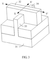
- FIG. 3 is a schematic structural diagram of a field-effect transistor according to an embodiment of the present invention.
- a gate 32 is disposed on a semiconductor substrate 31, a source drain area is located on two sides of the gate 32, and a fin source 33 and a fin drain 34 are respectively disposed on the two sides of the gate 32.
- an XX' direction is used to indicate a gate length direction of the field-effect transistor, to be specific, a transport direction of a carrier in the field-effect transistor;
- a YY' direction is used to indicate a gate structure (Gate structure) cross-sectional direction of the field-effect transistor, where the gate length direction and the gate structure cross-sectional direction are perpendicular to each other.
- an embodiment of the present invention provides a fabrication method of a field-effect transistor. As shown in FIG. 4 , the method includes the following steps.
- a support structure with a superlattice feature on a semiconductor substrate, where the support structure includes a first semiconductor material layer and a second semiconductor material layer that are alternately disposed, and an isolation layer is disposed on two sides of the support structure.
- the semiconductor substrate may be an SOI (Silicon-On-Insulator, silicon-on-insulator) substrate, a bulk silicon substrate, an ETSOI (Extremely Thin SOI, extremely thin SOI) substrate, an SGOI (SiGe-On-Insulator, SiGe-on-insulator) substrate, an III-V-OI (III-V-On-Insulator, III-V-on-insulator) substrate, or the like. This is not limited in this embodiment of the present invention.
- SOI Silicon-On-Insulator, silicon-on-insulator
- ETSOI Extremely Thin SOI, extremely thin SOI
- SGOI SiGe-On-Insulator, SiGe-on-insulator
- III-V-OI III-V-On-Insulator, III-V-on-insulator
- a thickness of the first semiconductor material layer 52 and a thickness of the second semiconductor material layer 53 may be both less than 50 nm.
- the first semiconductor material layer 52 is made of a silicon material
- the second semiconductor material layer 53 may be made of a silicon germanium material.
- the superlattice structure including the first semiconductor material layer 52 and the second semiconductor material layer 53 may be etched to form a support structure 61 shown in FIG. 6 .
- the support structure 61 is disposed on the semiconductor substrate 51 in a fin form.
- FIG. 6 (a) is a schematic cross-sectional view along a gate length direction
- FIG. 6 (b) is a schematic cross-sectional view along a gate structure cross-sectional direction.
- an isolation layer 71 is further formed on the two sides of the support structure 61, optionally by using a CMP (chemical-mechanical polishing) process and a recess (Recess) process.
- CMP chemical-mechanical polishing
- Recess recess
- a thickness of the isolation layer 71 is the same as a thickness of the etched semiconductor substrate 51.
- the isolation layer 71 may be specifically made of an oxide such as silicon oxide. This is not limited in this embodiment of the present invention.
- a dummy gate structure Form, along a boundary between the isolation layer and the support structure, a dummy gate structure that covers the support structure, where a length of the dummy gate structure in a gate length direction is less than a length of the first semiconductor material layer in the gate length direction.
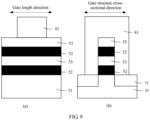
- FIG. 9 (a) a length of the dummy gate structure 81 in the gate length direction is less than a length of the first semiconductor material layer 52 in the gate length direction.
- FIG. 9 (a) is a schematic cross-sectional view along a gate length direction
- FIG. 9 (b) is a schematic cross-sectional view along a gate structure cross-sectional direction.
- the dummy gate structure 81 may be specifically made of a polycrystalline silicon material or an amorphous silicon material. This is not limited in this embodiment of the present invention.
- an insulation layer 91 may be further deposited on a periphery of the dummy gate structure 81, so that a side wall of the insulation layer 91 is flush with a side wall of the isolation layer 71 in the gate structure cross-sectional direction.
- FIG. 10 (a) is a schematic cross-sectional view along a gate length direction
- FIG. 10 (b) is a schematic cross-sectional view along a gate structure cross-sectional direction.
- the dummy gate structure 81 when the dummy gate structure 81 is formed, etching anisotropy is ensured as much as possible, and an etching selection ratio of polycrystalline silicon and silicon oxide is adjusted to be as high as possible, to form the dummy gate structure 81 in a relatively steep shape.
- the dummy gate structure 81 in the relatively steep shape facilitates subsequent forming of the insulation layer 91. Therefore, the dummy gate structure 81 can well fit with the insulation layer 91, thereby ensuring that the dummy gate structure 81 is effectively isolated.
- a dielectric constant of a dielectric filled in the insulation groove is less than a dielectric constant of the first semiconductor material layer.
- the first semiconductor material layer 52 and the second semiconductor material layer 53 may be first etched along the side wall of the insulation layer 91 in the gate length direction, so that side walls of the first semiconductor material layer 52 and the second semiconductor material layer 53 are flush with the side wall of the insulation layer 91 (as shown in FIG. 11 (a) ).
- FIG. 11 (a) is a schematic cross-sectional view along a gate length direction
- FIG. 11 (b) is a schematic cross-sectional view along a gate structure cross-sectional direction.
- a selective oxidation (selective oxidation) process is performed on the first semiconductor material layer 52 shown in FIG. 11 (a) . Therefore, in the first semiconductor material layer 52, the area other than the projection area of the dummy gate structure 81 in the first semiconductor material layer 52 is oxidized, and an oxidized part forms an insulation groove 101 shown in FIG. 12 (a) ; the projection area of the dummy gate structure 81 in the first semiconductor material layer 52 is not oxidized to form a sacrificial layer 102 shown in FIG. 12 (a) .
- the insulation groove 101 is filled with an oxide (for example, silicon oxide) of the first semiconductor material layer 52, and the oxide of the first semiconductor material layer 52 usually has a relatively low dielectric constant.
- the first semiconductor material layer 52 is made of silicon
- silicon oxide is formed in the insulation groove 101.
- a dielectric constant of the silicon oxide is approximately 3.9
- a dielectric constant of silicon is approximately 11.5, which is far greater than the dielectric constant of the silicon oxide.
- a selective etching process may be performed on the first semiconductor material layer 52 shown in FIG. 11 (a) along the gate length direction. Therefore, in the first semiconductor material layer 52, the area other than the projection area of the dummy gate structure 81 in the first semiconductor material layer 52 is removed to form the insulation groove 101 shown in FIG. 13 (a) ; the projection area of the dummy gate structure 81 in the first semiconductor material layer 52 is retained to form the sacrificial layer 102 shown in FIG. 13 (a) . In this case, the insulation groove 101 is filled with air.
- the air is a dielectric with a relatively low dielectric constant (a dielectric constant of the air is approximately 1).
- FIG. 13 (a) is a schematic cross-sectional view along a gate length direction
- FIG. 13 (b) is a schematic cross-sectional view along a gate structure cross-sectional direction.
- a dielectric material whose dielectric constant is less than 2.5 may be used as a low-K dielectric material, for example, SiCOH (a hydrogenated silicon carbon oxide).
- a dielectric material whose dielectric constant is greater than 4 may be used as a high-K dielectric material, for example, HfO 2 (hafnium dioxide).
- the dielectric constant of the first semiconductor material layer 52 or the second semiconductor material layer 53 is approximately 10 to 12.
- a material such as silicon or silicon germanium may epitaxially grow in a preset source drain area by using a selective epitaxy technology. Further, a doping process is used, so that the source drain area has a specified doping density, to form a source 131 and a drain 132 shown in FIG. 15 (FIG. 15 (a) is a schematic cross-sectional view along a gate length direction, and FIG. 15 (b) is a schematic cross-sectional view along a gate structure cross-sectional direction).
- the source 131 and the drain 132 are isolated from the sacrificial layer 102 through the insulation groove 101. Subsequently, after the sacrificial layer 102 is removed, a high-K dielectric material may be filled at a location of the sacrificial layer 102 to form a gate. In this way, the source 131 and the drain 132 can still be isolated from the gate through the insulation groove 101, to reduce a parasitic capacitance generated when the source 131 and the drain 132 are in direct contact with the gate.
- an impurity atom diffuses into the second semiconductor material layer 53 to form an extension area 133.
- a size of the extension area is related to a parasitic resistance of a field-effect transistor. A larger extension area indicates a smaller value of the parasitic resistance, and a smaller extension area indicates a larger value of the parasitic resistance.
- the thickness of the second semiconductor material layer 53 may be set as large as possible, to form a relatively large extension area.
- the larger thickness of the second semiconductor material layer 53 reduces a capability of the field-effect transistor to suppress a short-channel effect (Short-channel effects). For example, a leakage current of the field-effect transistor is increased.
- the foregoing problem may be resolved by using the following step 406.
- FIG. 16 is a schematic cross-sectional view along a gate length direction
- FIG. 16 (b) is a schematic cross-sectional view along a gate structure cross-sectional direction
- the foregoing dummy gate structure 81 and the sacrificial layer 102 may be removed by using an etching process.
- the location at which the first semiconductor material layer 51 is originally disposed in the gate 151 may be isolated from the source 131 (or the drain 132) by using a material with a relatively low dielectric constant in the insulation groove 101; the location at which the dummy gate structure 81 is originally disposed in the gate 151 may be isolated from the source 131 (or the drain 132) by using the insulation layer 91.
- the gate 151 is almost completely isolated from the source 131 (or the drain 132) through the insulation groove 101 and the insulation layer 91, to reduce a parasitic capacitance of the entire field-effect transistor, thereby improving performance and reliability of the field-effect transistor.
- an embodiment further provides a field-effect transistor, not forming part of the present invention.
- the field-effect transistor may be a MOSFET, a tunneling field-effect transistor, or the like.
- the gate 151 is disposed in a channel formed between the source 131 and the drain 132, and the gate 151 is not in direct contact with the source 131 (or the drain 132) but is isolated from the source 131 (or the drain 132) through the insulation groove 101.
- the insulation groove 101 is filled with a material with a relatively low dielectric constant. Therefore, a parasitic capacitance generated when the gate 151 is in direct contact with the source 131 (or the drain 132) can be avoided, and performance and reliability of the field-effect transistor can be improved.
- the functions described in the present invention may be implemented by using hardware, software, firmware, or any combination thereof.
- these functions may be stored in a computer readable medium or transmitted as one or more instructions or code in the computer readable medium.
- the computer readable medium includes a computer storage medium and a communications medium, where the communications medium includes any medium that enables a computer program to be transmitted from one place to another.
- the storage medium may be any available medium accessible to a general-purpose or dedicated computer.
Landscapes
- Engineering & Computer Science (AREA)
- Chemical & Material Sciences (AREA)
- Nanotechnology (AREA)
- Physics & Mathematics (AREA)
- Mathematical Physics (AREA)
- Theoretical Computer Science (AREA)
- Crystallography & Structural Chemistry (AREA)
- Insulated Gate Type Field-Effect Transistor (AREA)
- Thin Film Transistor (AREA)
Description
- Embodiments of the present invention relate to the field of semiconductor technologies, and in particular, to a field-effect transistor and a fabrication method of a field-effect transistor.
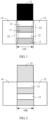
- Currently, when a field-effect transistor (FET) is fabricated, in an example of a MOSFET (Metal-Oxide Semiconductor Field-Effect Transistor), as shown in
FIG. 1 , generally, a firstsemiconductor material layer 11 and a secondsemiconductor material layer 12 are alternately stacked in achannel 100, adummy gate structure 13 is located on the secondsemiconductor material layer 12, and asource 14 and adrain 15 are formed in a source drain area on two sides of thechannel 100 by using a doping process. Then, the secondsemiconductor material layer 12 and thedummy gate structure 13 may be removed by using an etching process. Further, as shown inFIG. 2 , locations of the firstsemiconductor material layer 11 and thedummy gate structure 13 are filled with a gate material by using an RMG (Replacement Metal Gate, replacement metal gate) process, for example, a high dielectric constant (High-K) material, to form areal gate 21. - In the foregoing fabrication method, when the
source 14 and thedrain 15 are formed by using the doping process, as shown inFIG. 1 , the source 14 (or the drain 15) is in direct contact with the firstsemiconductor material layer 11 and the secondsemiconductor material layer 12 in thechannel 100. Consequently, some impurity atoms diffuse into the secondsemiconductor material layer 12 and the firstsemiconductor material layer 11 to form an extension (Extension)area 22. As a result, a parasitic parameter such as a parasitic capacitance of a subsequently formed MOSFET is increased, and a GIDL (gate-induced drain leakage) of the MOSFET is also increased, severely affecting performance and reliability of the MOSFET. -
US20150069328A1 describes a method of forming a semiconductor structure including: forming a stack of layers on a top surface of a substrate, the stack of layers including alternating layers of a semiconductor material and a sacrificial material, where a bottommost layer of the stack of layers is a top semiconductor layer of the substrate; patterning a plurality of material stacks from the stack of layers, each material stack including an alternating stack of a plurality of nanowire channels and a plurality of sacrificial spacers, the plurality of nanowire channels including the semiconductor material, and the plurality of sacrificial spacers including the sacrificial material; and removing at least one of the plurality of nanowire channels from at least one of the plurality of material stacks without removing one or more of the plurality of nanowire channels from an adjacent material stack. - In
US9362355B1 - In
US20160111495A1 , a method of forming a semiconductor device includes: forming a superlattice structure atop the top surface of a substrate, wherein the superlattice structure comprises a plurality of first layers and a corresponding plurality of second layers altematingly arranged in a plurality of stacked pairs; forming a lateral etch stop layer by epitaxial deposition of a material of the first layer or the second layer of the superlattice structure atop a sidewall of the superlattice structure, or by selectively oxidizing edges of the first layers and second layers of the superlattice structure; subsequently forming a source region adjacent a first end of the superlattice structure and a drain region adjacent a second opposing end of the superlattice structure; and selectively etching the superlattice structure to remove each of the first layers or each of the second layers to form a plurality of voids in the superlattice structure. - The present invention is defined by the claims.
- Embodiments of the present invention provide a fabrication method of a field-effect transistor, to reduce a parasitic parameter of a field-effect transistor, thereby improving performance and reliability of the field-effect transistor Also disclosed is a field-effect transistor manufactured according to the fabrication methods of the present invention.
- The following technical solutions are used in the embodiments of the present invention to achieve the foregoing objective.
- According to a first aspect, an embodiment of the present invention provides a fabrication method of a field-effect transistor, as set out in
claim 1. - In a possible design manner, the removing, along the gate length direction, an area other than a sacrificial layer in the first semiconductor material layer to form an insulation groove includes: performing, along the gate length direction, a selective oxidation process on the first semiconductor material layer, so that the area other than the sacrificial layer in the first semiconductor material layer is oxidized to form the insulation groove, where the dielectric filled in the insulation groove is an oxide of the first semiconductor material layer, and the oxide usually has a relatively low dielectric constant. Therefore, the insulation groove can isolate the subsequently formed source (or drain) from a high-K (high dielectric constant) dielectric material filled in the sacrificial layer, to avoid a parasitic capacitance generated after the source (or the drain) is in direct contact with the high-K dielectric material.
- In a possible design manner, the removing, along the gate length direction, an area other than a sacrificial layer in the first semiconductor material layer to form an insulation groove includes: performing, along the gate length direction, a selective etching process on the first semiconductor material layer, so that the area other than the sacrificial layer in the first semiconductor material layer is removed to form the insulation groove. In this case, the dielectric filled in the insulation groove is air with a relatively low dielectric constant. Therefore, the insulation groove can isolate the subsequently formed source (or drain) from the high-K dielectric material filled in the sacrificial layer, to avoid a parasitic capacitance generated after the source (or the drain) is in direct contact with the high-K dielectric material.
- In a possible design manner, after the insulation groove is formed, the method further includes: filling the insulation groove with a dielectric material whose dielectric constant is less than 3.9. In this case, the insulation groove is filled with the dielectric material whose dielectric constant is less than 3.9, to be specific, filled with a low-K dielectric material. Therefore, the insulation groove can isolate the subsequently formed source (or drain) from the high-K dielectric material filled in the sacrificial layer, to avoid a parasitic capacitance generated after the source (or the drain) is in direct contact with the high-K dielectric material.
- In a possible design manner, before the filling the insulation groove with a dielectric material whose dielectric constant is less than 3.9, the method further includes: forming, along the gate length direction, an etching stop layer on a surface of the insulation groove by using an ALD process. In this way, when the sacrificial layer is subsequently removed, the etching stop layer can prevent an etching solution from etching an area other than the sacrificial layer.
- In a possible design manner, the reducing a thickness of the second semiconductor material layer includes: reducing the thickness of the second semiconductor material layer from 8 nm to 4 nm by using an etching process.
- In a possible design manner, after the reducing a thickness of the second semiconductor material layer along a gate structure cross-sectional direction, the method further includes: forming a gate at locations of the removed dummy gate structure and the removed sacrificial layer by using an RMG process.
- In a possible design manner, the forming a support structure with a superlattice feature on a semiconductor substrate includes: growing a periodic superlattice structure including the first semiconductor material layer and the second semiconductor material layer that are alternately disposed on the semiconductor substrate, where a thickness of the first semiconductor material layer and the thickness of the second semiconductor material layer are both less than 50 nm; and etching the superlattice structure to form the fin support structure.
- In a possible design manner, the forming, along a boundary between the isolation layer and the support structure, a dummy gate structure that covers the support structure includes: forming an oxide layer on the exposed support structure; and forming, on the oxide layer, the dummy gate structure that covers the support structure.
- In a possible design manner, a length of the dummy gate structure in the gate structure cross-sectional direction is less than a length of the isolation layer; and after the dummy gate structure that covers the support structure is formed on the isolation layer, the method further includes: depositing an insulation layer on a periphery of the dummy gate structure, where a side wall of the insulation layer is flush with a side wall of the isolation layer.
- These aspects or other aspects of the present invention are more concise and understandable in the description of the following embodiments.
-
-
FIG. 1 is a schematic diagram 1 of a fabrication principle of a field-effect transistor in the prior art; -
FIG. 2 is a schematic diagram 2 of a fabrication principle of a field-effect transistor in the prior art; -
FIG. 3 is a schematic structural diagram of a field-effect transistor manufactured according to an embodiment of the present invention; -
FIG. 4 is a schematic flowchart of a fabrication method of a field-effect transistor according to an embodiment of the present invention; -
FIG. 5 is a schematic diagram 1 of a fabrication principle of a field-effect transistor according to an embodiment of the present invention; -
FIG. 6 is a schematic diagram 2 of a fabrication principle of a field-effect transistor according to an embodiment of the present invention; -
FIG. 7 is a schematic diagram 3 of a fabrication principle of a field-effect transistor according to an embodiment of the present invention; -
FIG. 8 is a schematic diagram 4 of a fabrication principle of a field-effect transistor according to an embodiment of the present invention; -
FIG. 9 is a schematic diagram 5 of a fabrication principle of a field-effect transistor according to an embodiment of the present invention; -
FIG. 10 is a schematic diagram 6 of a fabrication principle of a field-effect transistor according to an embodiment of the present invention; -
FIG. 11 is a schematic diagram 7 of a fabrication principle of a field-effect transistor according to an embodiment of the present invention; -
FIG. 12 is a schematic diagram 8 of a fabrication principle of a field-effect transistor according to an embodiment of the present invention; -
FIG. 13 is a schematic diagram 9 of a fabrication principle of a field-effect transistor according to an embodiment of the present invention; -
FIG. 14 is a schematic diagram 10 of a fabrication principle of a field-effect transistor according to an embodiment of the present invention; -
FIG. 15 is a schematic diagram 11 of a fabrication principle of a field-effect transistor according to an embodiment of the present invention; -
FIG. 16 is a schematic diagram 12 of a fabrication principle of a field-effect transistor according to an embodiment of the present invention; and -
FIG. 17 is a schematic diagram 13 of a fabrication principle of a field-effect transistor according to an embodiment of the present invention. - The following describes in detail the technical solutions in the embodiments of the present invention with reference to the accompanying drawings in the embodiments of the present invention. Apparently, the described embodiments are merely some but not all of the embodiments of the present invention.
- The examples not forming part of the present invention provide a field-effect transistor. The field-effect transistor may be a MOSFET such as a stacked gate-all-around nanowire transistor (Stacked Gate-All-Around Nanowire Transistor) or a fin field-effect transistor (Fin Field-effect transistor, FinFET), or may be a tunneling field-effect transistor (TFET, Tunneling Field-Effect Transistor) or the like.
- The embodiments of the present invention provide a fabrication method of a field-effect transistor. For ease of description, cross-sectional directions of the field-effect transistor are first explained.
FIG. 3 is a schematic structural diagram of a field-effect transistor according to an embodiment of the present invention. Agate 32 is disposed on asemiconductor substrate 31, a source drain area is located on two sides of thegate 32, and afin source 33 and afin drain 34 are respectively disposed on the two sides of thegate 32. In this case, an XX' direction is used to indicate a gate length direction of the field-effect transistor, to be specific, a transport direction of a carrier in the field-effect transistor; a YY' direction is used to indicate a gate structure (Gate structure) cross-sectional direction of the field-effect transistor, where the gate length direction and the gate structure cross-sectional direction are perpendicular to each other. - It should be noted that
FIG. 3 shows merely a structure including a group of thegate 32, thesource 33, and thedrain 34 in the field-effect transistor. It can be understood that the field-effect transistor may further include a plurality of groups of gates, sources, and drains that have similar structures as the foregoing gate, source, and drain. This is not limited in this embodiment of the present invention. - Based on the gate length direction and the gate structure cross-sectional direction shown in
FIG. 3 , an embodiment of the present invention provides a fabrication method of a field-effect transistor. As shown inFIG. 4 , the method includes the following steps. - 401. Form a support structure with a superlattice feature on a semiconductor substrate, where the support structure includes a first semiconductor material layer and a second semiconductor material layer that are alternately disposed, and an isolation layer is disposed on two sides of the support structure.
- The semiconductor substrate may be an SOI (Silicon-On-Insulator, silicon-on-insulator) substrate, a bulk silicon substrate, an ETSOI (Extremely Thin SOI, extremely thin SOI) substrate, an SGOI (SiGe-On-Insulator, SiGe-on-insulator) substrate, an III-V-OI (III-V-On-Insulator, III-V-on-insulator) substrate, or the like. This is not limited in this embodiment of the present invention.
- Specifically, as shown in
FIG. 5 (FIG. 5 (a) is a schematic cross-sectional view along a gate length direction, andFIG. 5 (b) is a schematic cross-sectional view along a gate structure cross-sectional direction), a periodic superlattice (superlattice) structure including a firstsemiconductor material layer 52 and a secondsemiconductor material layer 53 that are alternately disposed may be first grown on asemiconductor substrate 51. The superlattice structure is a strictly periodic multi-layer film that includes two different types of elements that are alternately stacked in forms of thin layers whose thicknesses range from several nanometers to tens of nanometers. - For example, a thickness of the first
semiconductor material layer 52 and a thickness of the secondsemiconductor material layer 53 may be both less than 50 nm. When the firstsemiconductor material layer 52 is made of a silicon material, the secondsemiconductor material layer 53 may be made of a silicon germanium material. - Further, the superlattice structure including the first
semiconductor material layer 52 and the secondsemiconductor material layer 53 may be etched to form asupport structure 61 shown inFIG. 6 . For example, thesupport structure 61 is disposed on thesemiconductor substrate 51 in a fin form. Herein,FIG. 6 (a) is a schematic cross-sectional view along a gate length direction, andFIG. 6 (b) is a schematic cross-sectional view along a gate structure cross-sectional direction. - Further, as shown in
FIG. 7 , anisolation layer 71 is further formed on the two sides of thesupport structure 61, optionally by using a CMP (chemical-mechanical polishing) process and a recess (Recess) process. - Optionally, a thickness of the
isolation layer 71 is the same as a thickness of the etchedsemiconductor substrate 51. - For example, the
isolation layer 71 may be specifically made of an oxide such as silicon oxide. This is not limited in this embodiment of the present invention. - 402. Form, along a boundary between the isolation layer and the support structure, a dummy gate structure that covers the support structure, where a length of the dummy gate structure in a gate length direction is less than a length of the first semiconductor material layer in the gate length direction.
- As shown in
FIG. 8 , after theisolation layer 71 is formed, adummy gate structure 81 that covers thesupport structure 61 may be further formed on theisolation layer 71. In this case, thesupport structure 61 is embedded in a gap formed between theisolation layer 71 and thedummy gate structure 81. - As shown in
FIG. 9 (a) , a length of thedummy gate structure 81 in the gate length direction is less than a length of the firstsemiconductor material layer 52 in the gate length direction. Herein,FIG. 9 (a) is a schematic cross-sectional view along a gate length direction, andFIG. 9 (b) is a schematic cross-sectional view along a gate structure cross-sectional direction. - For example, the
dummy gate structure 81 may be specifically made of a polycrystalline silicon material or an amorphous silicon material. This is not limited in this embodiment of the present invention. - Specifically, an oxide layer may be first formed on the exposed
support structure 61, and then thedummy gate structure 81 that covers thesupport structure 61 may be formed on the oxide layer. - Further, as shown in
FIG. 10 , aninsulation layer 91 may be further deposited on a periphery of thedummy gate structure 81, so that a side wall of theinsulation layer 91 is flush with a side wall of theisolation layer 71 in the gate structure cross-sectional direction. Herein,FIG. 10 (a) is a schematic cross-sectional view along a gate length direction, andFIG. 10 (b) is a schematic cross-sectional view along a gate structure cross-sectional direction. - In addition, when the
dummy gate structure 81 is formed, etching anisotropy is ensured as much as possible, and an etching selection ratio of polycrystalline silicon and silicon oxide is adjusted to be as high as possible, to form thedummy gate structure 81 in a relatively steep shape. Thedummy gate structure 81 in the relatively steep shape facilitates subsequent forming of theinsulation layer 91. Therefore, thedummy gate structure 81 can well fit with theinsulation layer 91, thereby ensuring that thedummy gate structure 81 is effectively isolated. - 403. Remove, along the gate length direction, an area other than a sacrificial layer in the first semiconductor material layer to form an insulation groove.
- The foregoing sacrificial layer is a projection area of the
dummy gate structure 81 in the firstsemiconductor material layer 52 along a target direction (the target direction is a direction perpendicular to a bottom of thesemiconductor substrate 51, to be specific, an orthographic projection direction of thedummy gate structure 81 in the first semiconductor material layer 52). - A dielectric constant of a dielectric filled in the insulation groove is less than a dielectric constant of the first semiconductor material layer.
- In a possible design manner, the first
semiconductor material layer 52 and the secondsemiconductor material layer 53 may be first etched along the side wall of theinsulation layer 91 in the gate length direction, so that side walls of the firstsemiconductor material layer 52 and the secondsemiconductor material layer 53 are flush with the side wall of the insulation layer 91 (as shown inFIG. 11 (a) ). Herein,FIG. 11 (a) is a schematic cross-sectional view along a gate length direction, andFIG. 11 (b) is a schematic cross-sectional view along a gate structure cross-sectional direction. - Further, a selective oxidation (selective oxidation) process is performed on the first
semiconductor material layer 52 shown inFIG. 11 (a) . Therefore, in the firstsemiconductor material layer 52, the area other than the projection area of thedummy gate structure 81 in the firstsemiconductor material layer 52 is oxidized, and an oxidized part forms aninsulation groove 101 shown inFIG. 12 (a) ; the projection area of thedummy gate structure 81 in the firstsemiconductor material layer 52 is not oxidized to form asacrificial layer 102 shown inFIG. 12 (a) . In this case, theinsulation groove 101 is filled with an oxide (for example, silicon oxide) of the firstsemiconductor material layer 52, and the oxide of the firstsemiconductor material layer 52 usually has a relatively low dielectric constant. Therefore, theinsulation groove 101 can isolate the subsequently formed source (or drain) from a gate material filled in thesacrificial layer 102, for example, a high-K (high dielectric constant) dielectric material, to avoid a parasitic capacitance generated after the subsequently formed source (or drain) is in direct contact with the gate formed by the gate material. Herein,FIG. 12 (a) is a schematic cross-sectional view along a gate length direction, andFIG. 12 (b) is a schematic cross-sectional view along a gate structure cross-sectional direction. - For example, when the first
semiconductor material layer 52 is made of silicon, after the foregoing selective oxidation process is performed, silicon oxide is formed in theinsulation groove 101. A dielectric constant of the silicon oxide is approximately 3.9, and a dielectric constant of silicon is approximately 11.5, which is far greater than the dielectric constant of the silicon oxide. - In another possible design manner, a selective etching process may be performed on the first
semiconductor material layer 52 shown inFIG. 11 (a) along the gate length direction. Therefore, in the firstsemiconductor material layer 52, the area other than the projection area of thedummy gate structure 81 in the firstsemiconductor material layer 52 is removed to form theinsulation groove 101 shown inFIG. 13 (a) ; the projection area of thedummy gate structure 81 in the firstsemiconductor material layer 52 is retained to form thesacrificial layer 102 shown inFIG. 13 (a) . In this case, theinsulation groove 101 is filled with air. The air is a dielectric with a relatively low dielectric constant (a dielectric constant of the air is approximately 1). Therefore, the air can isolate the subsequently formed source (or drain) from the gate material filled in thesacrificial layer 102, to avoid a parasitic capacitance generated after the subsequently formed source (or drain) is in direct contact with the gate formed by the gate material. Herein,FIG. 13 (a) is a schematic cross-sectional view along a gate length direction, andFIG. 13 (b) is a schematic cross-sectional view along a gate structure cross-sectional direction. - In addition, after the
insulation groove 101 shown inFIG. 13 (a) is formed, as shown inFIG. 14 (FIG. 14 (a) is a schematic cross-sectional view along a gate length direction, andFIG. 14 (b) is a schematic cross-sectional view along a gate structure cross-sectional direction), anetching stop layer 111 may be formed on a surface of theinsulation groove 101 by using an ALD (Atomic Layer Deposition, atomic layer deposition) process. In this way, when thesacrificial layer 102 is subsequently removed, theetching stop layer 111 can prevent an etching solution from etching an area other than thesacrificial layer 102. - Further, still as shown in
FIG. 14 (a) , theinsulation groove 101 may be filled with a dielectric material whose dielectric constant is less than 3.9, for example, a low-K (low dielectric constant)dielectric material 121, so that theinsulation groove 101 has a lower K (dielectric constant) value, to avoid a parasitic capacitance generated after the subsequently formed source (or drain) is in direct contact with the gate formed by the gate material filled in thesacrificial layer 102. - Generally, a dielectric material whose dielectric constant is less than 2.5 may be used as a low-K dielectric material, for example, SiCOH (a hydrogenated silicon carbon oxide).
- Similarly, a dielectric material whose dielectric constant is greater than 4 may be used as a high-K dielectric material, for example, HfO2 (hafnium dioxide).
- The dielectric constant (ε) described in this embodiment of the present invention is a product of a relative permittivity (εr) and an absolute vacuum permittivity (ε0), to be specific, ε=εr*ε0, where ε0=8.85*10-12 F/m.
- For example, the dielectric constant of the first
semiconductor material layer 52 or the secondsemiconductor material layer 53 is approximately 10 to 12. - 404. Form a source and a drain in a preset source drain area along the gate length direction, where the source and the drain are isolated from the sacrificial layer through the insulation groove.
- In an example in which a low-
K dielectric material 121 is filled in theinsulation groove 101 shown inFIG. 14 , instep 404, a material such as silicon or silicon germanium may epitaxially grow in a preset source drain area by using a selective epitaxy technology. Further, a doping process is used, so that the source drain area has a specified doping density, to form asource 131 and adrain 132 shown inFIG. 15 (FIG. 15 (a) is a schematic cross-sectional view along a gate length direction, andFIG. 15 (b) is a schematic cross-sectional view along a gate structure cross-sectional direction). - In this case, the
source 131 and thedrain 132 are isolated from thesacrificial layer 102 through theinsulation groove 101. Subsequently, after thesacrificial layer 102 is removed, a high-K dielectric material may be filled at a location of thesacrificial layer 102 to form a gate. In this way, thesource 131 and thedrain 132 can still be isolated from the gate through theinsulation groove 101, to reduce a parasitic capacitance generated when thesource 131 and thedrain 132 are in direct contact with the gate. - In addition, still as shown in
FIG. 15 (a) , when thesource 131 and thedrain 132 are formed, an impurity atom diffuses into the secondsemiconductor material layer 53 to form anextension area 133. A size of the extension area is related to a parasitic resistance of a field-effect transistor. A larger extension area indicates a smaller value of the parasitic resistance, and a smaller extension area indicates a larger value of the parasitic resistance. - Therefore, to reduce the parasitic resistance, the thickness of the second
semiconductor material layer 53 may be set as large as possible, to form a relatively large extension area. However, the larger thickness of the secondsemiconductor material layer 53 reduces a capability of the field-effect transistor to suppress a short-channel effect (Short-channel effects). For example, a leakage current of the field-effect transistor is increased. In this case, the foregoing problem may be resolved by using the followingstep 406. - 405. Remove the dummy gate structure and the sacrificial layer.
- As shown in
FIG. 16 (FIG. 16 (a) is a schematic cross-sectional view along a gate length direction, andFIG. 16 (b) is a schematic cross-sectional view along a gate structure cross-sectional direction), the foregoingdummy gate structure 81 and thesacrificial layer 102 may be removed by using an etching process. - 406. Adjust a thickness of the second semiconductor material layer along a gate structure cross-sectional direction.
- In
step 406, as shown inFIG. 16 (b) , the thickness of the secondsemiconductor material layer 53 in a channel area is reduced. For example, the thickness of the secondsemiconductor material layer 53 may be reduced from T1 of 8 nm to T2 of 4 nm by using an etching process or the like. In this way, because the channel effect of the field-effect transistor is related to the thickness of the secondsemiconductor material layer 53, the short-channel effect of the field-effect transistor can be alleviated by reducing the thickness of the secondsemiconductor material layer 53, so that the short-channel effect is flexibly adjusted without increasing a parasitic resistance. - 407. Form a gate at locations of the removed dummy gate structure and the removed sacrificial layer by using an RMG process.
- Subsequently, based on the prior art, a
gate 151 shown inFIG. 17 (thegate 151 includes a structure of at least two layers, where one layer is made of a high-K dielectric material, and the other layer is made of a metal material with a specific work function) may be formed at locations of the removeddummy gate structure 81 and the removedsacrificial layer 102 by using an RMG (Replacement Metal Gate, replacement metal gate) process, to finally form a field-effect transistor.FIG. 17 (a) is a schematic cross-sectional view along a gate length direction, andFIG. 17 (b) is a schematic cross-sectional view along a gate structure cross-sectional direction. - As shown in
FIG. 17 , in the formed field-effect transistor, the location at which the firstsemiconductor material layer 51 is originally disposed in thegate 151 may be isolated from the source 131 (or the drain 132) by using a material with a relatively low dielectric constant in theinsulation groove 101; the location at which thedummy gate structure 81 is originally disposed in thegate 151 may be isolated from the source 131 (or the drain 132) by using theinsulation layer 91. In other words, thegate 151 is almost completely isolated from the source 131 (or the drain 132) through theinsulation groove 101 and theinsulation layer 91, to reduce a parasitic capacitance of the entire field-effect transistor, thereby improving performance and reliability of the field-effect transistor. - In addition, an embodiment further provides a field-effect transistor, not forming part of the present invention. The field-effect transistor may be a MOSFET, a tunneling field-effect transistor, or the like.
- For a fabrication method of a field-effect transistor further provided in an embodiment of the present invention, refer to related content of
steps 401 to 407 in the foregoing embodiment. Therefore, details are not described herein again. - For example, as shown in
FIG. 17 (a) , in the field-effect transistor manufactured according to the method of the present invention, thegate 151 is disposed in a channel formed between thesource 131 and thedrain 132, and thegate 151 is not in direct contact with the source 131 (or the drain 132) but is isolated from the source 131 (or the drain 132) through theinsulation groove 101. Theinsulation groove 101 is filled with a material with a relatively low dielectric constant. Therefore, a parasitic capacitance generated when thegate 151 is in direct contact with the source 131 (or the drain 132) can be avoided, and performance and reliability of the field-effect transistor can be improved. - The embodiments of the present invention provide the fabrication method of the field-effect transistor. The fabrication method includes: first forming a support structure with a superlattice feature on a semiconductor substrate, where the support structure includes a first semiconductor material layer and a second semiconductor material layer that are alternately disposed, and an isolation layer is disposed on two sides of the support structure; further forming, on the isolation layer, a dummy gate structure that covers the support structure, where a length of the dummy gate structure in a gate length direction is less than a length of the first semiconductor material layer in the gate length direction; removing, along the gate length direction, an area other than a sacrificial layer in the first semiconductor material layer to form an insulation groove, where the insulation groove is formed in the area other than the sacrificial layer in the first semiconductor material layer, and the sacrificial layer is a projection area of the dummy gate structure in the first semiconductor material layer along a target direction (to be specific, a direction perpendicular to a surface of the isolation layer in which the support structure is disposed), and a dielectric constant of a dielectric filled in the insulation groove is less than a dielectric constant of the first semiconductor material layer; and forming a source and a drain in a preset source drain area along the gate length direction, where the source and the drain may be isolated, through the insulation groove, from a gate material (for example, a high-K dielectric material) filled in the sacrificial layer. Therefore, a parasitic capacitance generated when the source (or the drain) is in direct contact with the gate material can be avoided, a parasitic capacitance of the entire field-effect transistor can be reduced, and performance and reliability of the field-effect transistor can be improved.
- A person skilled in the art should be aware that in one or more of the foregoing examples, the functions described in the present invention may be implemented by using hardware, software, firmware, or any combination thereof. When the functions are implemented by software, these functions may be stored in a computer readable medium or transmitted as one or more instructions or code in the computer readable medium. The computer readable medium includes a computer storage medium and a communications medium, where the communications medium includes any medium that enables a computer program to be transmitted from one place to another. The storage medium may be any available medium accessible to a general-purpose or dedicated computer.
- The objectives, technical solutions, and beneficial effects of the present invention are further described in detail in the foregoing specific embodiments. It should be understood that the foregoing descriptions are merely specific embodiments of the present invention, but are not intended to limit the protection scope of the present invention, which is defined by the claims.
Claims (10)
- A fabrication method of a field-effect transistor, comprising:forming (401) a support structure (61) on a semiconductor substrate (51), wherein the support structure is a fin support structure comprising a strictly periodic multi-layer film that comprises a first semiconductor material layer (52) and a second semiconductor material layer (53) that are alternately disposed in a direction extending from the semiconductor substrate (51), wherein the first semiconductor material layer (52) and the second semiconductor material layer (53) each has a thickness in a range from several nanometers to tens of nanometers , and an isolation layer (71) is disposed in the semiconductor substrate (51) on two sides of the support structure (61);forming (402), along a boundary between the isolation layer (71) and the support structure (61), a dummy gate structure (81) that covers the support structure, wherein a length of the dummy gate structure (81) in a gate length direction is less than a length of the first semiconductor material layer (52) in the gate length direction, and the gate length direction is used to indicate a transport direction of a carrier in the field-effect transistor;removing (403), along the gate length direction, an area other than a sacrificial layer (102) in the first semiconductor material layer (52) to form an insulation groove (101), wherein the sacrificial layer (102) is a projection area of the dummy gate structure in the first semiconductor material layer (52) along a target direction, a dielectric constant of a dielectric filled in the insulation groove is less than a dielectric constant of the first semiconductor material layer, and the target direction is a direction perpendicular to a bottom of the semiconductor substrate;forming (404) a source (131)_and a drain (132) in a preset source drain area along the gate length direction, wherein the source and the drain are isolated from the sacrificial layer (102) through the insulation groove (101); andremoving (405) the dummy gate structure and the sacrificial layer,characterized by further comprising, after removing the dummy gate structure and the sacrificial layer, reducing (406) a thickness of the second semiconductor material, in a channel area, along a gate structure cross-sectional direction, where the gate structure cross-sectional direction is perpendicular to the gate length direction.
- The fabrication method according to claim 1, wherein the removing, along the gate length direction, an area other than a sacrificial layer in the first semiconductor material layer to form an insulation groove comprises:
performing, along the gate length direction, a selective oxidation process on the first semiconductor material layer (51), so that the area other than the sacrificial layer (102) in the first semiconductor material layer is oxidized to form the insulation groove (101), wherein the dielectric filled in the insulation groove is an oxide of the first semiconductor material layer. - The fabrication method according to claim 1, wherein the removing, along the gate length direction, an area other than a sacrificial layer in the first semiconductor material layer to form an insulation groove comprises:
performing, along the gate length direction, a selective etching process on the first semiconductor material layer (51), so that the area other than the sacrificial layer (102) in the first semiconductor material layer is removed to form the insulation groove (101). - The fabrication method according to claim 3, after the insulation groove is formed, further comprising:
filling the insulation groove with a dielectric material whose dielectric constant is less than 3.9. - The fabrication method according to claim 4, before the filling the insulation groove with a dielectric material whose dielectric constant is less than 3.9, further comprising:
forming, along the gate length direction, an etching stop layer on a surface of the insulation groove by using an atomic layer deposition, ALD, process. - The fabrication method according to any preceding claim, wherein the reducing a thickness of the second semiconductor material layer comprises:
reducing the thickness of the second semiconductor material layer from 8 nm to 4 nm by using an etching process. - The fabrication method according to any preceding claim, after the reducing a thickness of the second semiconductor material layer along a gate structure cross-sectional direction, further comprising:
forming a gate at locations of the removed dummy gate structure and the removed sacrificial layer by using a replacement metal gate RMG process. - The fabrication method according to any one of claims 1 to 7, wherein the forming a support structure on a semiconductor substrate comprises:growing a periodic structure comprising the first semiconductor material layer and the second semiconductor material layer that are alternately disposed on the semiconductor substrate, wherein a thickness of the first semiconductor material layer and the thickness of the second semiconductor material layer are both less than 50 nm; andetching the structure to form the fin support structure.
- The fabrication method according to any one of claims 1 to 8, wherein the forming, along a boundary between the isolation layer (71) and the support structure (81), a dummy gate structure (81) that covers the support structure comprises:forming an oxide layer on the exposed support structure; andforming, on the oxide layer, the dummy gate structure that covers the support structure.
- The fabrication method according to any one of claims 1 to 9, wherein a length of the dummy gate structure (81) in the gate structure cross-sectional direction is less than a length of the isolation layer (71); and
after the dummy gate structure that covers the support structure is formed on the isolation layer, the method further comprises:
depositing an insulation layer (91) on a periphery of the dummy gate structure (81), wherein a side wall of the insulation layer is flush with a side wall of the isolation layer (71).
Applications Claiming Priority (2)
| Application Number | Priority Date | Filing Date | Title |
|---|---|---|---|
| CN201611022835.2A CN106784001B (en) | 2016-11-21 | 2016-11-21 | Field-effect transistor and method of making the same |
| PCT/CN2017/088086 WO2018090607A1 (en) | 2016-11-21 | 2017-06-13 | Field effect transistor and manufacturing method therefor |
Publications (3)
| Publication Number | Publication Date |
|---|---|
| EP3534407A1 EP3534407A1 (en) | 2019-09-04 |
| EP3534407A4 EP3534407A4 (en) | 2019-11-20 |
| EP3534407B1 true EP3534407B1 (en) | 2023-12-20 |
Family
ID=58969939
Family Applications (1)
| Application Number | Title | Priority Date | Filing Date |
|---|---|---|---|
| EP17872453.0A Active EP3534407B1 (en) | 2016-11-21 | 2017-06-13 | Field effect transistor and manufacturing method therefor |
Country Status (4)
| Country | Link |
|---|---|
| US (2) | US11043575B2 (en) |
| EP (1) | EP3534407B1 (en) |
| CN (3) | CN111370466A (en) |
| WO (1) | WO2018090607A1 (en) |
Families Citing this family (21)
| Publication number | Priority date | Publication date | Assignee | Title |
|---|---|---|---|---|
| CN111370466A (en) | 2016-11-21 | 2020-07-03 | 华为技术有限公司 | Field effect transistor and manufacturing method thereof |
| US10211307B2 (en) * | 2017-07-18 | 2019-02-19 | Taiwan Semiconductor Manufacturing Co., Ltd. | Methods of manufacturing inner spacers in a gate-all-around (GAA) FET through multi-layer spacer replacement |
| DE102017124637B4 (en) | 2017-08-30 | 2025-03-27 | Taiwan Semiconductor Manufacturing Co., Ltd. | Manufacturing method for a semiconductor device and a semiconductor device |
| CN109904074B (en) * | 2017-12-11 | 2022-04-08 | 中芯国际集成电路制造(北京)有限公司 | Fully Surrounded Gate Field Effect Transistor and Method of Manufacturing the Same |
| CN110828541B (en) * | 2018-08-14 | 2023-05-16 | 中芯国际集成电路制造(北京)有限公司 | Semiconductor structures and methods of forming them |
| CN111180513B (en) * | 2018-11-12 | 2023-07-14 | 中芯国际集成电路制造(上海)有限公司 | Semiconductor device and method of forming the same |
| US11462614B2 (en) * | 2019-08-30 | 2022-10-04 | Taiwan Semiconductor Manufacturing Company, Ltd. | Semiconductor devices and methods of manufacturing |
| CN113690313A (en) * | 2020-05-18 | 2021-11-23 | 中芯国际集成电路制造(上海)有限公司 | Semiconductor structure and method of forming semiconductor structure |
| WO2022000257A1 (en) * | 2020-06-30 | 2022-01-06 | 华为技术有限公司 | Semiconductor device and manufacturing method therefor and electronic device |
| US11322505B2 (en) * | 2020-06-30 | 2022-05-03 | Taiwan Semiconductor Manufacturing Company, Ltd. | Ferroelectric random access memory devices and methods |
| WO2022032488A1 (en) * | 2020-08-11 | 2022-02-17 | 华为技术有限公司 | Field-effect transistor and manufacturing method therefor |
| US11289586B2 (en) * | 2020-08-11 | 2022-03-29 | Taiwan Semiconductor Manufacturing Co., Ltd. | Spacer structure for semiconductor device |
| CN112349592B (en) * | 2020-10-27 | 2022-07-19 | 中国科学院微电子研究所 | NS-FET for avoiding parasitic channel effect and preparation method thereof |
| CN112397581B (en) * | 2020-11-18 | 2022-06-10 | 光华临港工程应用技术研发(上海)有限公司 | Tunnel field effect transistor and manufacturing method thereof |
| WO2022205169A1 (en) * | 2021-03-31 | 2022-10-06 | 华为技术有限公司 | Field effect transistor and manufacturing method therefor, and switching circuit and circuit board |
| CN113284806B (en) * | 2021-05-18 | 2022-04-05 | 复旦大学 | Ring gate device, source-drain preparation method thereof, device preparation method and electronic equipment |
| CN115692461A (en) * | 2021-07-22 | 2023-02-03 | 北方集成电路技术创新中心(北京)有限公司 | Semiconductor structures and methods of forming them |
| US12224312B2 (en) * | 2021-08-25 | 2025-02-11 | International Business Machines Corporation | Field effect transistors with bottom dielectric isolation |
| CN116072542A (en) * | 2022-11-30 | 2023-05-05 | 中国科学院微电子研究所 | The preparation method of Huanshan TFET device |
| CN121240497A (en) * | 2024-06-24 | 2025-12-30 | 华为技术有限公司 | Chips and their fabrication methods, electronic devices |
| CN119342892B (en) * | 2024-09-19 | 2025-07-11 | 北京大学 | Preparation method of stacked transistor, stacked transistor and semiconductor device |
Family Cites Families (29)
| Publication number | Priority date | Publication date | Assignee | Title |
|---|---|---|---|---|
| JP4796329B2 (en) * | 2004-05-25 | 2011-10-19 | 三星電子株式会社 | Manufacturing method of multi-bridge channel type MOS transistor |
| KR100625177B1 (en) * | 2004-05-25 | 2006-09-20 | 삼성전자주식회사 | Manufacturing method of multi-bridge channel type MOS transistor |
| US20080076216A1 (en) * | 2006-09-25 | 2008-03-27 | Sangwoo Pae | Method to fabricate high-k/metal gate transistors using a double capping layer process |
| CN100530726C (en) * | 2007-11-30 | 2009-08-19 | 华南师范大学 | III-V family metal oxide semiconductor luminous fieldistor and method for producing the same |
| FR2945891B1 (en) * | 2009-05-19 | 2011-07-15 | Commissariat Energie Atomique | SEMICONDUCTOR STRUCTURE AND METHOD FOR PRODUCING SEMICONDUCTOR STRUCTURE. |
| US8753942B2 (en) * | 2010-12-01 | 2014-06-17 | Intel Corporation | Silicon and silicon germanium nanowire structures |
| CN107039281B (en) * | 2011-12-22 | 2021-06-18 | 英特尔公司 | Semiconductor device with necked semiconductor body and method of forming semiconductor bodies of different widths |
| US9281378B2 (en) * | 2012-01-24 | 2016-03-08 | Taiwan Semiconductor Manufacturing Company, Ltd. | Fin recess last process for FinFET fabrication |
| US8994002B2 (en) * | 2012-03-16 | 2015-03-31 | Taiwan Semiconductor Manufacturing Company, Ltd. | FinFET having superlattice stressor |
| US9484447B2 (en) | 2012-06-29 | 2016-11-01 | Intel Corporation | Integration methods to fabricate internal spacers for nanowire devices |
| KR102002380B1 (en) * | 2012-10-10 | 2019-07-23 | 삼성전자 주식회사 | Semiconductor device and fabricated method thereof |
| KR102033579B1 (en) * | 2013-01-25 | 2019-10-17 | 삼성전자주식회사 | A semiconductor device having nanowire channel structure and method of manufacturing the same |
| GB2526457B (en) * | 2013-03-15 | 2018-08-22 | Intel Corp | Nanowire transistor with underlayer etch stops |
| US9184269B2 (en) * | 2013-08-20 | 2015-11-10 | Taiwan Semiconductor Manufacturing Company Limited | Silicon and silicon germanium nanowire formation |
| US9257545B2 (en) * | 2013-09-12 | 2016-02-09 | Globalfoundries Inc. | Stacked nanowire device with variable number of nanowire channels |
| US9508796B2 (en) | 2013-10-03 | 2016-11-29 | Intel Corporation | Internal spacers for nanowire transistors and method of fabrication thereof |
| US9431512B2 (en) * | 2014-06-18 | 2016-08-30 | Globalfoundries Inc. | Methods of forming nanowire devices with spacers and the resulting devices |
| US9673277B2 (en) * | 2014-10-20 | 2017-06-06 | Applied Materials, Inc. | Methods and apparatus for forming horizontal gate all around device structures |
| US9711414B2 (en) * | 2014-10-21 | 2017-07-18 | Samsung Electronics Co., Ltd. | Strained stacked nanosheet FETS and/or quantum well stacked nanosheet |
| US9502673B2 (en) | 2015-03-31 | 2016-11-22 | International Business Machines Corporation | Transistor devices with tapered suspended vertical arrays of carbon nanotubes |
| US9362355B1 (en) * | 2015-11-13 | 2016-06-07 | International Business Machines Corporation | Nanosheet MOSFET with full-height air-gap spacer |
| US9748404B1 (en) * | 2016-02-29 | 2017-08-29 | International Business Machines Corporation | Method for fabricating a semiconductor device including gate-to-bulk substrate isolation |
| CN111370466A (en) * | 2016-11-21 | 2020-07-03 | 华为技术有限公司 | Field effect transistor and manufacturing method thereof |
| US9997519B1 (en) * | 2017-05-03 | 2018-06-12 | International Business Machines Corporation | Dual channel structures with multiple threshold voltages |
| US10074575B1 (en) * | 2017-06-21 | 2018-09-11 | International Business Machines Corporation | Integrating and isolating nFET and pFET nanosheet transistors on a substrate |
| US10957601B2 (en) * | 2018-10-11 | 2021-03-23 | International Business Machines Corporation | Self-aligned fin recesses in nanosheet field effect transistors |
| US10734286B1 (en) * | 2019-02-07 | 2020-08-04 | International Business Machines Corporation | Multiple dielectrics for gate-all-around transistors |
| US10700064B1 (en) * | 2019-02-15 | 2020-06-30 | International Business Machines Corporation | Multi-threshold voltage gate-all-around field-effect transistor devices with common gates |
| US10998234B2 (en) * | 2019-05-14 | 2021-05-04 | International Business Machines Corporation | Nanosheet bottom isolation and source or drain epitaxial growth |
-
2016
- 2016-11-21 CN CN202010121987.8A patent/CN111370466A/en active Pending
- 2016-11-21 CN CN202010100849.1A patent/CN111370489A/en active Pending
- 2016-11-21 CN CN201611022835.2A patent/CN106784001B/en active Active
-
2017
- 2017-06-13 EP EP17872453.0A patent/EP3534407B1/en active Active
- 2017-06-13 WO PCT/CN2017/088086 patent/WO2018090607A1/en not_active Ceased
-
2019
- 2019-05-20 US US16/417,544 patent/US11043575B2/en active Active
-
2021
- 2021-06-18 US US17/352,161 patent/US11664440B2/en active Active
Also Published As
| Publication number | Publication date |
|---|---|
| CN111370466A (en) | 2020-07-03 |
| US20210313451A1 (en) | 2021-10-07 |
| CN106784001A (en) | 2017-05-31 |
| US20190280104A1 (en) | 2019-09-12 |
| CN106784001B (en) | 2020-02-21 |
| EP3534407A1 (en) | 2019-09-04 |
| WO2018090607A1 (en) | 2018-05-24 |
| US11664440B2 (en) | 2023-05-30 |
| US11043575B2 (en) | 2021-06-22 |
| CN111370489A (en) | 2020-07-03 |
| EP3534407A4 (en) | 2019-11-20 |
Similar Documents
| Publication | Publication Date | Title |
|---|---|---|
| US11664440B2 (en) | Field-effect transistor and fabrication method of field-effect transistor | |
| US9082851B2 (en) | FinFET having suppressed leakage current | |
| CN104576383B (en) | A kind of FinFET structure and manufacturing method thereof | |
| US9443854B2 (en) | FinFET with constrained source-drain epitaxial region | |
| US8575708B2 (en) | Structure of field effect transistor with fin structure | |
| CN103928334B (en) | Semiconductor device and manufacturing method thereof | |
| US8853013B2 (en) | Method for fabricating field effect transistor with fin structure | |
| US9679962B2 (en) | FinFET and method of manufacturing the same | |
| US11404325B2 (en) | Silicon and silicon germanium nanowire formation | |
| US20110201164A1 (en) | Method of Dual EPI Process For Semiconductor Device | |
| US8722501B2 (en) | Method for manufacturing multi-gate transistor device | |
| CN104517847B (en) | Nodeless mesh body pipe and forming method thereof | |
| US12237371B2 (en) | Method for forming a semiconductor device | |
| US20140291761A1 (en) | Asymmetric Spacers | |
| CN111341661B (en) | Transistors and methods of forming them | |
| CN103839814A (en) | Method for forming fin field effect transistor | |
| CN104103506B (en) | Semiconductor device manufacturing method | |
| US20230197831A1 (en) | Method for Forming a Semiconductor Device | |
| US8440511B1 (en) | Method for manufacturing multi-gate transistor device | |
| CN112018184A (en) | Device with ferroelectric or negative capacitance material, method of manufacturing the same, and electronic apparatus | |
| CN115763371B (en) | Semiconductor structure and forming method thereof | |
| US20160204199A1 (en) | Mosfet structure and manufacturing method thereof | |
| CN119562559A (en) | Semiconductor structure and method of forming the same | |
| CN121126823A (en) | A semiconductor structure and its formation method | |
| TWI529804B (en) | Semiconductor structure with metal gate and method of fabricating the same |
Legal Events
| Date | Code | Title | Description |
|---|---|---|---|
| STAA | Information on the status of an ep patent application or granted ep patent |
Free format text: STATUS: THE INTERNATIONAL PUBLICATION HAS BEEN MADE |
|
| PUAI | Public reference made under article 153(3) epc to a published international application that has entered the european phase |
Free format text: ORIGINAL CODE: 0009012 |
|
| STAA | Information on the status of an ep patent application or granted ep patent |
Free format text: STATUS: REQUEST FOR EXAMINATION WAS MADE |
|
| 17P | Request for examination filed |
Effective date: 20190531 |
|
| AK | Designated contracting states |
Kind code of ref document: A1 Designated state(s): AL AT BE BG CH CY CZ DE DK EE ES FI FR GB GR HR HU IE IS IT LI LT LU LV MC MK MT NL NO PL PT RO RS SE SI SK SM TR |
|
| AX | Request for extension of the european patent |
Extension state: BA ME |
|
| A4 | Supplementary search report drawn up and despatched |
Effective date: 20191018 |
|
| RIC1 | Information provided on ipc code assigned before grant |
Ipc: H01L 29/78 20060101AFI20191014BHEP Ipc: H01L 21/336 20060101ALI20191014BHEP Ipc: H01L 29/76 20060101ALI20191014BHEP Ipc: H01L 29/423 20060101ALI20191014BHEP Ipc: H01L 29/06 20060101ALI20191014BHEP Ipc: B82Y 10/00 20110101ALI20191014BHEP Ipc: H01L 29/66 20060101ALI20191014BHEP |
|
| DAV | Request for validation of the european patent (deleted) | ||
| DAX | Request for extension of the european patent (deleted) | ||
| STAA | Information on the status of an ep patent application or granted ep patent |
Free format text: STATUS: EXAMINATION IS IN PROGRESS |
|
| 17Q | First examination report despatched |
Effective date: 20211014 |
|
| GRAP | Despatch of communication of intention to grant a patent |
Free format text: ORIGINAL CODE: EPIDOSNIGR1 |
|
| STAA | Information on the status of an ep patent application or granted ep patent |
Free format text: STATUS: GRANT OF PATENT IS INTENDED |
|
| RIC1 | Information provided on ipc code assigned before grant |
Ipc: H01L 29/786 20060101ALI20230619BHEP Ipc: H01L 29/76 20060101ALI20230619BHEP Ipc: H01L 29/775 20060101ALI20230619BHEP Ipc: H01L 29/423 20060101ALI20230619BHEP Ipc: B82Y 10/00 20110101ALI20230619BHEP Ipc: H01L 29/06 20060101ALI20230619BHEP Ipc: H01L 21/336 20060101ALI20230619BHEP Ipc: H01L 29/78 20060101AFI20230619BHEP |
|
| INTG | Intention to grant announced |
Effective date: 20230706 |
|
| GRAS | Grant fee paid |
Free format text: ORIGINAL CODE: EPIDOSNIGR3 |
|
| GRAA | (expected) grant |
Free format text: ORIGINAL CODE: 0009210 |
|
| STAA | Information on the status of an ep patent application or granted ep patent |
Free format text: STATUS: THE PATENT HAS BEEN GRANTED |
|
| AK | Designated contracting states |
Kind code of ref document: B1 Designated state(s): AL AT BE BG CH CY CZ DE DK EE ES FI FR GB GR HR HU IE IS IT LI LT LU LV MC MK MT NL NO PL PT RO RS SE SI SK SM TR |
|
| REG | Reference to a national code |
Ref country code: GB Ref legal event code: FG4D |
|
| REG | Reference to a national code |
Ref country code: CH Ref legal event code: EP |
|
| REG | Reference to a national code |
Ref country code: DE Ref legal event code: R096 Ref document number: 602017077790 Country of ref document: DE |
|
| REG | Reference to a national code |
Ref country code: IE Ref legal event code: FG4D |
|
| PG25 | Lapsed in a contracting state [announced via postgrant information from national office to epo] |
Ref country code: GR Free format text: LAPSE BECAUSE OF FAILURE TO SUBMIT A TRANSLATION OF THE DESCRIPTION OR TO PAY THE FEE WITHIN THE PRESCRIBED TIME-LIMIT Effective date: 20240321 |
|
| REG | Reference to a national code |
Ref country code: LT Ref legal event code: MG9D |
|
| PG25 | Lapsed in a contracting state [announced via postgrant information from national office to epo] |
Ref country code: LT Free format text: LAPSE BECAUSE OF FAILURE TO SUBMIT A TRANSLATION OF THE DESCRIPTION OR TO PAY THE FEE WITHIN THE PRESCRIBED TIME-LIMIT Effective date: 20231220 |
|
| REG | Reference to a national code |
Ref country code: NL Ref legal event code: MP Effective date: 20231220 |
|
| PG25 | Lapsed in a contracting state [announced via postgrant information from national office to epo] |
Ref country code: ES Free format text: LAPSE BECAUSE OF FAILURE TO SUBMIT A TRANSLATION OF THE DESCRIPTION OR TO PAY THE FEE WITHIN THE PRESCRIBED TIME-LIMIT Effective date: 20231220 |
|
| PG25 | Lapsed in a contracting state [announced via postgrant information from national office to epo] |
Ref country code: LT Free format text: LAPSE BECAUSE OF FAILURE TO SUBMIT A TRANSLATION OF THE DESCRIPTION OR TO PAY THE FEE WITHIN THE PRESCRIBED TIME-LIMIT Effective date: 20231220 Ref country code: GR Free format text: LAPSE BECAUSE OF FAILURE TO SUBMIT A TRANSLATION OF THE DESCRIPTION OR TO PAY THE FEE WITHIN THE PRESCRIBED TIME-LIMIT Effective date: 20240321 Ref country code: FI Free format text: LAPSE BECAUSE OF FAILURE TO SUBMIT A TRANSLATION OF THE DESCRIPTION OR TO PAY THE FEE WITHIN THE PRESCRIBED TIME-LIMIT Effective date: 20231220 Ref country code: ES Free format text: LAPSE BECAUSE OF FAILURE TO SUBMIT A TRANSLATION OF THE DESCRIPTION OR TO PAY THE FEE WITHIN THE PRESCRIBED TIME-LIMIT Effective date: 20231220 Ref country code: BG Free format text: LAPSE BECAUSE OF FAILURE TO SUBMIT A TRANSLATION OF THE DESCRIPTION OR TO PAY THE FEE WITHIN THE PRESCRIBED TIME-LIMIT Effective date: 20240320 |
|
| PG25 | Lapsed in a contracting state [announced via postgrant information from national office to epo] |
Ref country code: NL Free format text: LAPSE BECAUSE OF FAILURE TO SUBMIT A TRANSLATION OF THE DESCRIPTION OR TO PAY THE FEE WITHIN THE PRESCRIBED TIME-LIMIT Effective date: 20231220 |
|
| PG25 | Lapsed in a contracting state [announced via postgrant information from national office to epo] |
Ref country code: SE Free format text: LAPSE BECAUSE OF FAILURE TO SUBMIT A TRANSLATION OF THE DESCRIPTION OR TO PAY THE FEE WITHIN THE PRESCRIBED TIME-LIMIT Effective date: 20231220 Ref country code: RS Free format text: LAPSE BECAUSE OF FAILURE TO SUBMIT A TRANSLATION OF THE DESCRIPTION OR TO PAY THE FEE WITHIN THE PRESCRIBED TIME-LIMIT Effective date: 20231220 Ref country code: NO Free format text: LAPSE BECAUSE OF FAILURE TO SUBMIT A TRANSLATION OF THE DESCRIPTION OR TO PAY THE FEE WITHIN THE PRESCRIBED TIME-LIMIT Effective date: 20240320 Ref country code: NL Free format text: LAPSE BECAUSE OF FAILURE TO SUBMIT A TRANSLATION OF THE DESCRIPTION OR TO PAY THE FEE WITHIN THE PRESCRIBED TIME-LIMIT Effective date: 20231220 Ref country code: LV Free format text: LAPSE BECAUSE OF FAILURE TO SUBMIT A TRANSLATION OF THE DESCRIPTION OR TO PAY THE FEE WITHIN THE PRESCRIBED TIME-LIMIT Effective date: 20231220 Ref country code: HR Free format text: LAPSE BECAUSE OF FAILURE TO SUBMIT A TRANSLATION OF THE DESCRIPTION OR TO PAY THE FEE WITHIN THE PRESCRIBED TIME-LIMIT Effective date: 20231220 |
|
| PG25 | Lapsed in a contracting state [announced via postgrant information from national office to epo] |
Ref country code: IS Free format text: LAPSE BECAUSE OF FAILURE TO SUBMIT A TRANSLATION OF THE DESCRIPTION OR TO PAY THE FEE WITHIN THE PRESCRIBED TIME-LIMIT Effective date: 20240420 |
|
| PG25 | Lapsed in a contracting state [announced via postgrant information from national office to epo] |
Ref country code: CZ Free format text: LAPSE BECAUSE OF FAILURE TO SUBMIT A TRANSLATION OF THE DESCRIPTION OR TO PAY THE FEE WITHIN THE PRESCRIBED TIME-LIMIT Effective date: 20231220 |
|
| PG25 | Lapsed in a contracting state [announced via postgrant information from national office to epo] |
Ref country code: SK Free format text: LAPSE BECAUSE OF FAILURE TO SUBMIT A TRANSLATION OF THE DESCRIPTION OR TO PAY THE FEE WITHIN THE PRESCRIBED TIME-LIMIT Effective date: 20231220 |
|
| PG25 | Lapsed in a contracting state [announced via postgrant information from national office to epo] |
Ref country code: SM Free format text: LAPSE BECAUSE OF FAILURE TO SUBMIT A TRANSLATION OF THE DESCRIPTION OR TO PAY THE FEE WITHIN THE PRESCRIBED TIME-LIMIT Effective date: 20231220 Ref country code: SK Free format text: LAPSE BECAUSE OF FAILURE TO SUBMIT A TRANSLATION OF THE DESCRIPTION OR TO PAY THE FEE WITHIN THE PRESCRIBED TIME-LIMIT Effective date: 20231220 Ref country code: RO Free format text: LAPSE BECAUSE OF FAILURE TO SUBMIT A TRANSLATION OF THE DESCRIPTION OR TO PAY THE FEE WITHIN THE PRESCRIBED TIME-LIMIT Effective date: 20231220 Ref country code: IT Free format text: LAPSE BECAUSE OF FAILURE TO SUBMIT A TRANSLATION OF THE DESCRIPTION OR TO PAY THE FEE WITHIN THE PRESCRIBED TIME-LIMIT Effective date: 20231220 Ref country code: IS Free format text: LAPSE BECAUSE OF FAILURE TO SUBMIT A TRANSLATION OF THE DESCRIPTION OR TO PAY THE FEE WITHIN THE PRESCRIBED TIME-LIMIT Effective date: 20240420 Ref country code: EE Free format text: LAPSE BECAUSE OF FAILURE TO SUBMIT A TRANSLATION OF THE DESCRIPTION OR TO PAY THE FEE WITHIN THE PRESCRIBED TIME-LIMIT Effective date: 20231220 Ref country code: CZ Free format text: LAPSE BECAUSE OF FAILURE TO SUBMIT A TRANSLATION OF THE DESCRIPTION OR TO PAY THE FEE WITHIN THE PRESCRIBED TIME-LIMIT Effective date: 20231220 |
|
| PG25 | Lapsed in a contracting state [announced via postgrant information from national office to epo] |
Ref country code: PL Free format text: LAPSE BECAUSE OF FAILURE TO SUBMIT A TRANSLATION OF THE DESCRIPTION OR TO PAY THE FEE WITHIN THE PRESCRIBED TIME-LIMIT Effective date: 20231220 Ref country code: PT Free format text: LAPSE BECAUSE OF FAILURE TO SUBMIT A TRANSLATION OF THE DESCRIPTION OR TO PAY THE FEE WITHIN THE PRESCRIBED TIME-LIMIT Effective date: 20240422 |
|
| PG25 | Lapsed in a contracting state [announced via postgrant information from national office to epo] |
Ref country code: PT Free format text: LAPSE BECAUSE OF FAILURE TO SUBMIT A TRANSLATION OF THE DESCRIPTION OR TO PAY THE FEE WITHIN THE PRESCRIBED TIME-LIMIT Effective date: 20240422 Ref country code: PL Free format text: LAPSE BECAUSE OF FAILURE TO SUBMIT A TRANSLATION OF THE DESCRIPTION OR TO PAY THE FEE WITHIN THE PRESCRIBED TIME-LIMIT Effective date: 20231220 |
|
| REG | Reference to a national code |
Ref country code: DE Ref legal event code: R097 Ref document number: 602017077790 Country of ref document: DE |
|
| PG25 | Lapsed in a contracting state [announced via postgrant information from national office to epo] |
Ref country code: DK Free format text: LAPSE BECAUSE OF FAILURE TO SUBMIT A TRANSLATION OF THE DESCRIPTION OR TO PAY THE FEE WITHIN THE PRESCRIBED TIME-LIMIT Effective date: 20231220 |
|
| PLBE | No opposition filed within time limit |
Free format text: ORIGINAL CODE: 0009261 |
|
| STAA | Information on the status of an ep patent application or granted ep patent |
Free format text: STATUS: NO OPPOSITION FILED WITHIN TIME LIMIT |
|
| PG25 | Lapsed in a contracting state [announced via postgrant information from national office to epo] |
Ref country code: SI Free format text: LAPSE BECAUSE OF FAILURE TO SUBMIT A TRANSLATION OF THE DESCRIPTION OR TO PAY THE FEE WITHIN THE PRESCRIBED TIME-LIMIT Effective date: 20231220 |
|
| PG25 | Lapsed in a contracting state [announced via postgrant information from national office to epo] |
Ref country code: SI Free format text: LAPSE BECAUSE OF FAILURE TO SUBMIT A TRANSLATION OF THE DESCRIPTION OR TO PAY THE FEE WITHIN THE PRESCRIBED TIME-LIMIT Effective date: 20231220 Ref country code: DK Free format text: LAPSE BECAUSE OF FAILURE TO SUBMIT A TRANSLATION OF THE DESCRIPTION OR TO PAY THE FEE WITHIN THE PRESCRIBED TIME-LIMIT Effective date: 20231220 |
|
| REG | Reference to a national code |
Ref country code: DE Ref legal event code: R079 Ref document number: 602017077790 Country of ref document: DE Free format text: PREVIOUS MAIN CLASS: H01L0029780000 Ipc: H10D0030600000 |
|
| 26N | No opposition filed |
Effective date: 20240923 |
|
| PG25 | Lapsed in a contracting state [announced via postgrant information from national office to epo] |
Ref country code: MC Free format text: LAPSE BECAUSE OF FAILURE TO SUBMIT A TRANSLATION OF THE DESCRIPTION OR TO PAY THE FEE WITHIN THE PRESCRIBED TIME-LIMIT Effective date: 20231220 |
|
| REG | Reference to a national code |
Ref country code: CH Ref legal event code: PL |
|
| PG25 | Lapsed in a contracting state [announced via postgrant information from national office to epo] |
Ref country code: LU Free format text: LAPSE BECAUSE OF NON-PAYMENT OF DUE FEES Effective date: 20240613 |
|
| PG25 | Lapsed in a contracting state [announced via postgrant information from national office to epo] |
Ref country code: IE Free format text: LAPSE BECAUSE OF NON-PAYMENT OF DUE FEES Effective date: 20240613 |
|
| PG25 | Lapsed in a contracting state [announced via postgrant information from national office to epo] |
Ref country code: CH Free format text: LAPSE BECAUSE OF NON-PAYMENT OF DUE FEES Effective date: 20240630 Ref country code: BE Free format text: LAPSE BECAUSE OF NON-PAYMENT OF DUE FEES Effective date: 20240630 |
|
| REG | Reference to a national code |
Ref country code: BE Ref legal event code: MM Effective date: 20240630 |
|
| PGFP | Annual fee paid to national office [announced via postgrant information from national office to epo] |
Ref country code: DE Payment date: 20250429 Year of fee payment: 9 |
|
| PGFP | Annual fee paid to national office [announced via postgrant information from national office to epo] |
Ref country code: GB Payment date: 20250501 Year of fee payment: 9 |
|
| PGFP | Annual fee paid to national office [announced via postgrant information from national office to epo] |
Ref country code: FR Payment date: 20250508 Year of fee payment: 9 |
|
| PGFP | Annual fee paid to national office [announced via postgrant information from national office to epo] |
Ref country code: AT Payment date: 20250528 Year of fee payment: 9 |
|
| PG25 | Lapsed in a contracting state [announced via postgrant information from national office to epo] |
Ref country code: CY Free format text: LAPSE BECAUSE OF FAILURE TO SUBMIT A TRANSLATION OF THE DESCRIPTION OR TO PAY THE FEE WITHIN THE PRESCRIBED TIME-LIMIT; INVALID AB INITIO Effective date: 20170613 |
|
| PG25 | Lapsed in a contracting state [announced via postgrant information from national office to epo] |
Ref country code: HU Free format text: LAPSE BECAUSE OF FAILURE TO SUBMIT A TRANSLATION OF THE DESCRIPTION OR TO PAY THE FEE WITHIN THE PRESCRIBED TIME-LIMIT; INVALID AB INITIO Effective date: 20170613 |