EP3534198A1 - Microscope having three-dimensional imaging capability and imaging method - Google Patents
Microscope having three-dimensional imaging capability and imaging method Download PDFInfo
- Publication number
- EP3534198A1 EP3534198A1 EP16919938.7A EP16919938A EP3534198A1 EP 3534198 A1 EP3534198 A1 EP 3534198A1 EP 16919938 A EP16919938 A EP 16919938A EP 3534198 A1 EP3534198 A1 EP 3534198A1
- Authority
- EP
- European Patent Office
- Prior art keywords
- excitation
- microscope
- sample
- detection
- imaging
- Prior art date
- Legal status (The legal status is an assumption and is not a legal conclusion. Google has not performed a legal analysis and makes no representation as to the accuracy of the status listed.)
- Withdrawn
Links
Images



Classifications
-
- G—PHYSICS
- G02—OPTICS
- G02B—OPTICAL ELEMENTS, SYSTEMS OR APPARATUS
- G02B21/00—Microscopes
- G02B21/0004—Microscopes specially adapted for specific applications
- G02B21/002—Scanning microscopes
- G02B21/0024—Confocal scanning microscopes (CSOMs) or confocal "macroscopes"; Accessories which are not restricted to use with CSOMs, e.g. sample holders
- G02B21/0036—Scanning details, e.g. scanning stages
-
- G—PHYSICS
- G02—OPTICS
- G02B—OPTICAL ELEMENTS, SYSTEMS OR APPARATUS
- G02B21/00—Microscopes
-
- G—PHYSICS
- G02—OPTICS
- G02B—OPTICAL ELEMENTS, SYSTEMS OR APPARATUS
- G02B21/00—Microscopes
- G02B21/0004—Microscopes specially adapted for specific applications
- G02B21/002—Scanning microscopes
- G02B21/0024—Confocal scanning microscopes (CSOMs) or confocal "macroscopes"; Accessories which are not restricted to use with CSOMs, e.g. sample holders
- G02B21/0028—Confocal scanning microscopes (CSOMs) or confocal "macroscopes"; Accessories which are not restricted to use with CSOMs, e.g. sample holders specially adapted for specific applications, e.g. for endoscopes, ophthalmoscopes, attachments to conventional microscopes
-
- G—PHYSICS
- G02—OPTICS
- G02B—OPTICAL ELEMENTS, SYSTEMS OR APPARATUS
- G02B21/00—Microscopes
- G02B21/0004—Microscopes specially adapted for specific applications
- G02B21/002—Scanning microscopes
- G02B21/0024—Confocal scanning microscopes (CSOMs) or confocal "macroscopes"; Accessories which are not restricted to use with CSOMs, e.g. sample holders
- G02B21/0032—Optical details of illumination, e.g. light-sources, pinholes, beam splitters, slits, fibers
-
- G—PHYSICS
- G02—OPTICS
- G02B—OPTICAL ELEMENTS, SYSTEMS OR APPARATUS
- G02B21/00—Microscopes
- G02B21/0004—Microscopes specially adapted for specific applications
- G02B21/002—Scanning microscopes
- G02B21/0024—Confocal scanning microscopes (CSOMs) or confocal "macroscopes"; Accessories which are not restricted to use with CSOMs, e.g. sample holders
- G02B21/0052—Optical details of the image generation
-
- G—PHYSICS
- G02—OPTICS
- G02B—OPTICAL ELEMENTS, SYSTEMS OR APPARATUS
- G02B21/00—Microscopes
- G02B21/0004—Microscopes specially adapted for specific applications
- G02B21/002—Scanning microscopes
- G02B21/0024—Confocal scanning microscopes (CSOMs) or confocal "macroscopes"; Accessories which are not restricted to use with CSOMs, e.g. sample holders
- G02B21/0052—Optical details of the image generation
- G02B21/006—Optical details of the image generation focusing arrangements; selection of the plane to be imaged
-
- G—PHYSICS
- G02—OPTICS
- G02B—OPTICAL ELEMENTS, SYSTEMS OR APPARATUS
- G02B21/00—Microscopes
- G02B21/0004—Microscopes specially adapted for specific applications
- G02B21/002—Scanning microscopes
- G02B21/0024—Confocal scanning microscopes (CSOMs) or confocal "macroscopes"; Accessories which are not restricted to use with CSOMs, e.g. sample holders
- G02B21/008—Details of detection or image processing, including general computer control
-
- G—PHYSICS
- G02—OPTICS
- G02B—OPTICAL ELEMENTS, SYSTEMS OR APPARATUS
- G02B21/00—Microscopes
- G02B21/06—Means for illuminating specimens
-
- G—PHYSICS
- G02—OPTICS
- G02B—OPTICAL ELEMENTS, SYSTEMS OR APPARATUS
- G02B21/00—Microscopes
- G02B21/16—Microscopes adapted for ultraviolet illumination ; Fluorescence microscopes
-
- G—PHYSICS
- G02—OPTICS
- G02B—OPTICAL ELEMENTS, SYSTEMS OR APPARATUS
- G02B21/00—Microscopes
- G02B21/36—Microscopes arranged for photographic purposes or projection purposes or digital imaging or video purposes including associated control and data processing arrangements
- G02B21/365—Control or image processing arrangements for digital or video microscopes
- G02B21/367—Control or image processing arrangements for digital or video microscopes providing an output produced by processing a plurality of individual source images, e.g. image tiling, montage, composite images, depth sectioning, image comparison
-
- G—PHYSICS
- G01—MEASURING; TESTING
- G01N—INVESTIGATING OR ANALYSING MATERIALS BY DETERMINING THEIR CHEMICAL OR PHYSICAL PROPERTIES
- G01N21/00—Investigating or analysing materials by the use of optical means, i.e. using sub-millimetre waves, infrared, visible or ultraviolet light
- G01N21/62—Systems in which the material investigated is excited whereby it emits light or causes a change in wavelength of the incident light
- G01N21/63—Systems in which the material investigated is excited whereby it emits light or causes a change in wavelength of the incident light optically excited
- G01N21/65—Raman scattering
- G01N2021/653—Coherent methods [CARS]
- G01N2021/655—Stimulated Raman
-
- G—PHYSICS
- G01—MEASURING; TESTING
- G01N—INVESTIGATING OR ANALYSING MATERIALS BY DETERMINING THEIR CHEMICAL OR PHYSICAL PROPERTIES
- G01N21/00—Investigating or analysing materials by the use of optical means, i.e. using sub-millimetre waves, infrared, visible or ultraviolet light
- G01N21/62—Systems in which the material investigated is excited whereby it emits light or causes a change in wavelength of the incident light
- G01N21/63—Systems in which the material investigated is excited whereby it emits light or causes a change in wavelength of the incident light optically excited
- G01N21/636—Systems in which the material investigated is excited whereby it emits light or causes a change in wavelength of the incident light optically excited using an arrangement of pump beam and probe beam; using the measurement of optical non-linear properties
-
- G—PHYSICS
- G01—MEASURING; TESTING
- G01N—INVESTIGATING OR ANALYSING MATERIALS BY DETERMINING THEIR CHEMICAL OR PHYSICAL PROPERTIES
- G01N21/00—Investigating or analysing materials by the use of optical means, i.e. using sub-millimetre waves, infrared, visible or ultraviolet light
- G01N21/62—Systems in which the material investigated is excited whereby it emits light or causes a change in wavelength of the incident light
- G01N21/63—Systems in which the material investigated is excited whereby it emits light or causes a change in wavelength of the incident light optically excited
- G01N21/64—Fluorescence; Phosphorescence
- G01N21/645—Specially adapted constructive features of fluorimeters
- G01N21/6456—Spatial resolved fluorescence measurements; Imaging
- G01N21/6458—Fluorescence microscopy
-
- G—PHYSICS
- G01—MEASURING; TESTING
- G01N—INVESTIGATING OR ANALYSING MATERIALS BY DETERMINING THEIR CHEMICAL OR PHYSICAL PROPERTIES
- G01N21/00—Investigating or analysing materials by the use of optical means, i.e. using sub-millimetre waves, infrared, visible or ultraviolet light
- G01N21/62—Systems in which the material investigated is excited whereby it emits light or causes a change in wavelength of the incident light
- G01N21/63—Systems in which the material investigated is excited whereby it emits light or causes a change in wavelength of the incident light optically excited
- G01N21/65—Raman scattering
-
- G—PHYSICS
- G02—OPTICS
- G02B—OPTICAL ELEMENTS, SYSTEMS OR APPARATUS
- G02B2207/00—Coding scheme for general features or characteristics of optical elements and systems of subclass G02B, but not including elements and systems which would be classified in G02B6/00 and subgroups
- G02B2207/114—Two photon or multiphoton effect
Definitions
- the present disclosure generally relate to the technical field of imaging microscope and microscopic imaging method, and in particular, to a high-throughput three-dimensional digital-imaging microscope and a high-throughput three-dimensional microscopic digital-imaging method both of which are mainly applicable to biological and medical technology fields.
- Three-dimensional digital imaging is an important content of modern microscopy. And a three-dimensional microscopy has a vital pursuit of imaging relatively more samples in a non-destructive manner, on the premise that the resolution thereof is not decreased.
- the three-dimensional digital imaging may detect a sample by a method which produces a contrast response (e.g., fluorescent light), i.e., a step of excitation, and may record the contrasts by another method, i.e., a step of a photoelectric conversion and digitization, and may in turn digitizing a respective one of the contrasts for each volume element within a detection target region to be detected into a respective voxel (also referred to as "volumetric pixel" which is three-dimensional) which serves as a final throughput.
- a contrast response e.g., fluorescent light
- another method i.e., a step of a photoelectric conversion and digitization
- a respective voxel also referred to as "volumetric pixel" which is three-dimensional
- the specific number of voxels is defined to be a volume of the detection target region divided by a volume (the volume is determined by a required resolution) corresponding to the voxel, and thus the specific number of voxels cooperates with a digitization speed to determine an upper limit of the speed of the three-dimensional digital imaging.
- a practical imaging speed in the prior art is far from reaching such an upper limit.
- a size of a three-dimensional voxel is set corresponding to a sample unit of 1 micrometer ⁇ 1 micrometer ⁇ 1 micrometer (i.e., a sub-cellular resolution), with an upper limit of the digital imaging speed which should be 1250 seconds, i.e., approximating to 21 minutes; and alternatively the voxel is set corresponding to a sample unit of 5 micrometers ⁇ 5 micrometers ⁇ 5 micrometers (i.e., a soma resolution), with an upper limit of the digital imaging speed which may merely require 10 seconds.
- a representative speed for imaging a mouse brain in a condition of a sub-micron resolution may be 3 days ( Gong, H. et al. Nat. Commun. 7:12142, 2016 ); and a speed as a latest result in a condition of a soma resolution may be about 2 hours ( Li Ye, et al., Cell, 165 (7), 16 June 2016 ,).
- a speed of the excitation nor the speed of the recording is a bottle-neck issue.
- an important reason for causing such a difference lies in that it may be inevitable to incur a pause or a stop in the process of the imaging, such that an effective imaging time may be shortened.
- a prior imaging technology typically adopts such a solution that:
- a mass of interruptions to imaging are involved therein.
- a time may be required for each movement itself; and a time may be required for further waiting for waiting for dissipation or vanishment of vibration caused by start/restart, or pause/stop, then imaging processes may proceed again, resulting in relatively long interruptions in imaging processes.
- specific number of above interruptions in imaging may be increased at a cubic power, which may seriously influence imaging efficiency.
- a portion of technologies may take advantages of solutions such as an electric focusing lens and the like to decrease the time of interruptions in imaging, but these solutions may merely be adapted to the z direction, and have relatively large restrictions in scale, partially improving the throughput of the three-dimensional digital imaging.
- Figs. 1A to 1G illustrates solutions typically adopted for implementing three-dimensional imaging in prior art:
- a main purpose to be solved by the disclosure is to provided a microscope having three-dimensional imaging capability and a three-dimensional microscopic imaging method, which may improve effectively imaging time and implementing a high-throughput three-dimensional microscopy.
- a microscope having three-dimensional imaging capability comprising:
- any imaging blurring incurred by potentially existing movement may be simple and consistent, for example, such that the blurring may be readily eliminated by de-convolution and the like.
- each of sample units is merely excited by the at least one excitation device for not longer than a time period in which a displacement of each of sample units due to the relative movement is not more than a requirement in resolution of the microscope, each sample unit being corresponding to a respective one of voxels which are imaged.
- the blurring incurred by relative movement is negligible.
- an environment where the sample is located is filled with a transparent material having its refractive index similar or equal to a refractive index of the sample.
- the at least one excitation device comprises an excitation light source selected from a group comprising: one or more light-emitting diodes, one or more continuous lasers, one or more pulsed lasers, or any combination thereof.
- the detectable contrast is a signal selected from a group comprising one of the following: fluorescent light, elastic scattering light, Raman scattering, SHG, THG, stimulated Raman scattering, or a combination thereof.
- the at least one excitation device is configured to excite the sample by using light-sheet illumination with a pulse having a pulse time not longer than the time period.
- the at least one excitation device is constructed as a pulsed light source which comprises: one or more pulsed lasers, one or more light-emitting diodes operating at a pulsed mode, or a continuum light source modulated in various manners, or any combination thereof.
- the at least one excitation device and the at least one detection device are configured to operate synchronously with each other.
- the at least one excitation device further comprises an optical shaping device which comprises: one or more cylindrical mirrors, one or more cylindrical lenses, one or more anamorphotic lenses, one or more transmission phase devices, or one or more reflection phase devices; and the at least one excitation device is configured to form the light-sheet illumination.
- an optical shaping device which comprises: one or more cylindrical mirrors, one or more cylindrical lenses, one or more anamorphotic lenses, one or more transmission phase devices, or one or more reflection phase devices; and the at least one excitation device is configured to form the light-sheet illumination.
- the at least one excitation device generates at least one excitation light beam propagating in the detection target region in the excitation principal axis direction which is approximately perpendicular to a detection direction of the at least one detection device.
- the at least one excitation device comprises at least one scanning mechanism which is configured to perform scanning by moving the excitation light beam.
- the excitation light beam is shaped to have a beam radius which has a varying rate of not more than 3 times within the detection target region in a direction of the light beam.
- the at least one scanning mechanism comprises one or more galvanometer scanners, one or more resonant scanning mirrors, one or more rotating polygonal mirror, one or more acousto-optic modulators, or any combination thereof
- the at least one detection device uses a matrix photosensitive device to function as the imaging device configured to operate synchronously with the scanning mechanism.
- the at least one detection device comprises a de-scanning mechanism which is configured to operate synchronously with the scanning mechanism, and is provided with an array photosensitive device or a matrix photosensitive device to function as the imaging device.
- the at least one excitation device comprises a beam splitter which is configured to split the excitation light beam into a plurality of excitation sub-beams.
- the beam splitter comprises a combination of one or more lens arrays, one or more mirror arrays, one or more semi-transparent mirrors or a combination thereof, or comprises a fixed or adjustable phase filter or a digital micro mirror device (abbreviated as DMD) array.
- DMD digital micro mirror device
- the at least one excitation device and the at least one detection device are configured to form collectively a structure for confocal scanning microscopy.
- a three-dimensional microscopic imaging method comprising:
- the three-dimensional microscopic imaging method further comprises eliminating blurring incurred by the relative movement with a de-convolution algorithm.
- the device and method according to the disclosure may enhance three-dimensional imaging throughput in a condition of a same resolution.
- an apparatus and a method may be illustrated, allowing an implementation of imaging without any pause or stop, i.e., an uninterrupted imaging, in the first type relative movement, minimizing any existence of the second type relative movement, resulting in an increased effective imaging time, and an enhanced imaging throughput.
- a core technical concept of the disclosure lies in decreasing unnecessary pause or stop in imaging processes. Furthermore, focusing on and conceiving around such core technical concept, a combination of a series of technologies may be used, with fundamental contents containing: by moving the sample while performing substantially uninterrupted imaging processes simultaneously, then, decreasing switching operations each of which occurs between adjacent fields of view and interrupts the imaging processes, eliminating blur incurred by movements of the sample during imaging processes in above implementations, and improving aberration and the like incurred in above implementations.
- a microscope having three-dimensional imaging capability which is configured to perform a three-dimensional detection and imaging on a sample, comprising: at least one excitation device, which is configured to generate a detectable contrast in detection target region of the sample which is to be detected, in an excitation principal axis direction; at least one detection device, which is configured to detect the contrast as generated from the detection target region of the sample in a detection principal axis, without eliminating a possibility that the detection device shares its components with the excitation device; and at least one movement mechanism, which is configured to generate a relative movement of the sample relative to the at least one excitation device and the at least one detection device.
- any irregular dithering incurred by speed change, start, or pause or stop may be eliminated.
- any blurring incurred by still existing movement may be simple and consistent, such that the blurring may be readily eliminated by de-convolution method and the like.
- each sample unit which corresponds to each voxel to be formed by imaging may merely be excited by the at least one excitation device for not longer than a certain time period; and in the certain time period, a displacement of each of sample units due to the relative movement is not more than a requirement in resolution of the microscope. As such, blurring incurred by the relative movement(s) may be negligible.
- an environment where the sample is located may be filled with a transparent material having its refractive index similar or approximately equal to a refractive index of the sample.
- the excitation device may use one or more light-emitting diodes, one or more continuous lasers, one or more pulsed lasers, or any combination thereof to function as an excitation light source.
- the detectable contrast may for example be fluorescent light, elastic scattering light, Raman scattering, SHG, THG, stimulated Raman scattering, or the like, or a combination thereof.
- the at least one detection device may use dot, array or matrix device(s) consisting of CCD photosensitive elements, CMOS photosensitive elements, photodiodes (abbreviated as PD, including avalanche photodiodes (abbreviated as APD), photomultipliers), or any combination thereof to function as photosensitive devices.
- the at least one excitation device may use a pulse having a pulse time not longer than the certain time period; and the at least one detection device may use a matrix photosensitive devices such as a CCD camera, a CMOS camera, or the like to function as an imaging device.
- a matrix photosensitive devices such as a CCD camera, a CMOS camera, or the like to function as an imaging device.
- the at least one excitation device may comprise: one or more cylindrical mirrors, one or more cylindrical lens, one or more anamorphotic lenses, one or more transmission phase devices, or one or more reflection phase devices; and the optical shaping device is configured to form the light-sheet illumination.
- a pulsed light source may comprise: one or more pulsed lasers, one or more light-emitting diodes operating at a pulsed mode, or a continuum light source modulated in various manners. And the pulsed light source for example operates synchronously with the imaging device.
- the at least one excitation device generates at least one excitation light beam approximately perpendicular to a detection direction of the at least one detection device; and the at least one excitation device comprises at least one scanning mechanism which is configured to perform scanning by moving the excitation light beam.
- the excitation light beam may have a beam radius having a varying rate of not more than 3 times within the detection target region in a direction of the light beam.
- One implementation of the at least one scanning mechanism lies in that, it comprises one or more galvanometer scanners, one or more resonant scanning mirrors, one or more rotating polygonal mirror, one or more acousto-optic modulators, or any combination thereof.
- the at least one detection device for example comprises a matrix photosensitive device such as a CCD camera, a CMOS camera, or the like to function as the imaging device which is configured to operate synchronously with the scanning mechanism.
- the at least one detection device may comprise a de-scanning mechanism which is configured to operate synchronously with the scanning mechanism, and the de-scanning mechanism is for example provided with an array photosensitive device or a matrix photosensitive device, such as an LED array, a CCD camera, a CMOS camera to function as the imaging device.
- the at least one excitation device for example comprises a beam splitter configured to split the excitation light beam into a plurality of excitation sub-beams.
- the beam splitter for example comprises a combination of one or more lens arrays, one or more mirror arrays, one or more semi-transparent mirror (i.e., half transparent and half reflecting mirror, or transflective mirror) arrays, or comprises a fixed or adjustable phase filter or a digital micro mirror device (abbreviated as DMD) array.
- DMD digital micro mirror device
- the at least one excitation device and the at least one detection device are configured to cooperate with each other to form collectively a structure for confocal scanning microscopy.
- a three-dimensional microscopic imaging method comprising:
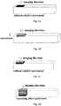
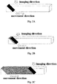
- Figs. 2A to 2C illustrate an operation principle of three-dimensional imaging of the disclosure.
- a continuous relative movement at a constant speed is for example maintained between the sample and the the imaging system, a direction of the relative movement is neither parallel to nor coincide with an imaging direction
- Fig. 2A illustrates an example in which a movement direction is at an angle of 45° with respect to the imaging direction; as illustrated in Figs. 2B and 2C , in the disclosure, imaging processes are carried out continuously and uninterruptedly at new locations of a sample of a relatively large scale, until a three-dimensional imaging of the sample is finalized.
- Fig. 3 illustrates a three-dimensional imaging microscope, which has a resolution requirement of 1 micrometer as for a sample having a thickness of 300 micrometers.
- fluorescent light is taken as an example for a contrast which is relied on during the imaging.
- the contrast of the fluorescent light is supplied by excitation of fluorescent protein such as GFP and the like with a laser beam having a wavelength of 488 micrometer.
- the excitation device 1 and the detection device 2 may adopt symmetric multiplex structures, respectively, as appropriate; in other words, both sides may be provided with excitation and detection functionalities.
- the left side is simplified as a pure excitation device, while the right side funtions as a detection device.
- principal axes of respective optical paths of the excitation device 1 and the detection device 2 may for example be perpendicular to each other, and each of the excitation device 1 and the detection device 2 may form an angle of 45° with respect to a horizontal plane (upper surface of the table, floor).
- the sample table 3 is parallel to the horizontal plane, and configured to carry and move the sample to the imaging position, such that the sample may continuously and successively move horizontally upon imaging.
- Respective front ends of the excitation device 1 and the detection device 2 are objective lenses, respectively.
- each has a numerical aperture of 0.5 and a work distance of 3.5mm.
- a laser beam having a wavelength of 488 micrometers, which serves as the excitation light 4 may pass through a telescope or a stop/diaphragm configured to perform both intensity adjustment and beam-diameter adjustment, and then be incident onto a galvanometer scanner 5, so as to generate a linear excitation light which scans in a plane perpendicular to the detection direction, behind the objective lens 10.
- Relay lenses 6, 7 are configured that the galvanometer scanner 5 and a back focal plane of the lens 10 are conjugate.
- Mirrors 8, 9 are configured to turn and twist scanning light rays, and hereby save space.
- the mirror 9 is required to be a dichroic mirror which allows a long wave to pass therethrough.
- the excitation device 1 converges the excitation light beam at a position labeled by reference sign "11" within the sample as illustrated, so as to excite a fluorescent light.
- An effective numerical aperture of the excitation device 1 is in a range of 0.03 to 0.04, so as to ensure that the converged excitation light beam has a beam waist radius of a varying rate of not more than 2 times, within a range of about 420 micrometers around a location having a minimum value of the beam waist radius.
- the detection device 2 images the position labeled by reference sign "11", and core elements of the detection device 2 are as follows, i.e., an objective lens 12, a tube lens 13 (which has a focal length of 125 millimeters) and a camera 14 (Hamamatsu Flash4.0s CMOS camera).
- the camera has a number of pixels of 2048 ⁇ 2048, and a pixel size of 6.5 micrometers ⁇ 6.5 micrometers, with a full-frame frame rate of 100Hz, i.e., 10 milliseconds per frame.
- the galvanometer scanner 5 is configured to perform scanning synchronously with a saw-tooth wave having a unidirectional rate of 10 milliseconds.
- the sample table 3 moves at a speed of 100 micrometers per second, i.e., 1 micrometer per frame. Blurring incurred by the movement is less than 1/200, and thus is ignored.
- the sample has a target refractive index of 1.45 for index matching, and an optical matching solution may for example comprise HistoDenz.
- the whole system may require about 16 minutes for completing a three-dimensional imaging for a sample having a size of 1 centimeter ⁇ 1 centimeter, at a resolution of 1 micrometer; it may require about 5 to 6 hours for implementing a fluorescence imaging for a whole brain of a mouse, which is significantly superior to prior art. Figs.
- FIG. 4A to 4C illustrates an instance of a fluorescence imaging for a whole brain of a mouse as acquired by the system; specifically, Fig. 4A illustrates a coronal sectional view by a three-dimensional reconstruction of a imaging result for a brain slice having a thickness of hundreds of micrometers, Fig. 4B illustrates fine structures of neuron somas and neuron dendrites in a relatively small range of the brain slice, and Fig. 4C illustrates fine structures of neuron axons and the like which are captured in a certain imaging plane.
- a pulsed light source is applied to provide light-sheet illumination.
- the pulsed light source 4 takes a nanosecond nitrogen molecule/dye laser having an operating frequency of 30 to 100 Hz as an example, the exited laser beam may for example pass through a telescope or a stop/diaphragm configured to perform both intensity adjustment and beam-diameter adjustment so as to form a rectangular light beam which is incident on a cylindrical mirror 5.
- the cylindrical mirror has a focal length of 100 millimeters, and is configured that its cylindrical face is perpendicular to a plane which is defined collectively by principal axes of respective optical paths of the excitation device 1 and the detection device 2.
- FIG. 5 Other devices are similar to those in the system as illustrated in Fig. 3 .
- An image capture by a camera is performed synchronously with the pulsed light source.
- the system as illustrated in Fig. 5 has a three-dimensional imaging capability similar to that of the system as illustrated in Fig. 3 .
- a multi-photon scanning imaging structure is adopted.
- the excitation device 1 and the detection device 2 may share devices at their respective front end portions.
- a principal axis of the excitation device 1 forms an angle of 45° with respect to a direction perpendicular to an upper surface of the table (also to the floor), and a principal axis of the detection device 2 also forms an angle of 45°with respect to a direction perpendicular to an upper surface of the table (also to the floor).
- the sample table 3 is arranged parallel to the upper surface of the table, and configured to carry and move the sample to the imaging position, such that the sample may continuously and successively move horizontally upon imaging.
- Respective front ends of the excitation device 1 and the detection device 2 may be an objective lens 10 (a type of Olympus UMPLFLN 20XW) having as a numerical aperture of 0.5 and a work distance of 3.5mm.
- a pulsed excitation light 4 for generating a multi-photon excitation is typically a femtosecond laser or a picosecond laser, and may pass through a telescope or a stop/diaphragm configured to perform both intensity adjustment and beam-diameter adjustment, and then be incident onto a two-dimensional scanning mechanism 5, for generating a dotted excitation which scans in a plane perpendicular to the detection direction, behind the objective lens 10.
- Relay lenses 6, 7 are configured that the galvanometer scanner 5 and a back focal plane of the objective lens 10 are conjugate.
- Mirrors 8, 9 are configured to turn and twist scanning light rays, and hereby save space.
- the mirror 9 is a dichroic mirror which allows a long wave to pass therethrough.
- An effective numerical aperture of the excitation device 1 is 0.5.
- the excitation device 1 carries out the excitation at a position labeled by reference sign "11" within the sample as illustrated.
- the detection device 2 images the position labeled by reference sign "11", i.e., the imaging position, with its core devices similar to those in the system as illustrated in Fig. 5 .
- the system may apply to a condition in which SNR (i.e., signal to noise ratio) requirement is higher than speed.
- a beam splitter is inserted into an optical path of the excitation light 4 before entering the scanning mechanism 5, and is configured to split the excitation light beam into a plurality of excitation sub-beams, and at the same time to excite various sub-regions within a range at the imaging position 11, so as to accelerate total scanning speed.
- the detection device thereof may for example use high-speed detectors of other type, e.g., photodiodes (abbreviated as PD, including avalanche photodiodes (abbreviated as APD), photomultipliers or the like).
- PD photodiodes
- APD avalanche photodiodes
- photomultipliers or the like
- a portion of devices which are shared at respective front ends of the excitation device 1 and the detection device 2 may for example comprise the objective lens to the scanning mechanism in an upstream direction; then, in a detection portion which is provided separately, a conjugate pinhole or aperture may be added at a position conjugated with the sample, so as to form collectively a structure for confocal scanning microscopy.
- the excitation device may for example adopt an excitation light source, which may for example be: one or more light-emitting diodes, one or more continuous lasers, one or more pulsed lasers, or any combination thereof.
- an excitation light source which may for example be: one or more light-emitting diodes, one or more continuous lasers, one or more pulsed lasers, or any combination thereof.
- the contrast which is relied on during the imaging may be: one of the following: fluorescent light, elastic scattering light, Raman scattering, SHG, THG, stimulated Raman scattering, or the like.
- the angle may be selected flexibly depending on specific requirements, mainly for being adapted to a contact angle of the objective lens as selected.
- an objective lens having a relatively larger numeral aperture may be chosen; and for being adapted thereto, the angle between the detection direction and the direction of the relative movement may be selected to be in a range of 55° to 65°.
- the specific form of the relative movement may not be limited to a linear relative movement.
- a relative movement in a form of a circumferential movement may be another preferable form.
- Fig. 7A illustrates nano-scale fluorescent beads photographed in a stationary state
- Fig. 7B illustrates a situation of an exposure lasting for 10 milliseconds during a movement of 1 millimeter per second, from which it can be seen that there may exist obvious and consistent blurring incurred by the movement
- a de-convolution processing details of the image may be recovered from Fig. 7B , with its result being shown in Fig.
- the blurring incurred by the movement may be suppressed, by restricting excitation time, with a main idea of ensuring that a movement of each point of the sample during the excitation time may be ignored as compared with the resolution requirement; briefly speaking, it is only required to ensure that a product of the excitation time multiplied by the movement speed is significantly smaller than a minimal scale which is resolvable. If the resolution requirement is 1 micrometer, and the movement speed is 1 millimeter per second, then the excitation time is required to be less than 1 millisecond. A pulsed light source having a proper pulse width may directly satisfy such a requirement.
- the continuum light source may provide illumination by a proper switch modulation; more effectively, the continuum light source may also for example implement an excitation of a point in a relatively short time period by scanning.
- a field of view of a microscope may have a width of 2000 pixels.
- a linear excitation light may have a width of about 10 pixels.
- a sample having a relatively larger thickness may be lack of transparency, and there may also exist a relatively larger aberration during the imaging simultaneously.
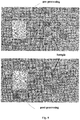
- Fig. 9 illustrates a contrast between a pre-processing effect and a post-processing effect.
Landscapes
- Physics & Mathematics (AREA)
- General Physics & Mathematics (AREA)
- Optics & Photonics (AREA)
- Chemical & Material Sciences (AREA)
- Analytical Chemistry (AREA)
- Engineering & Computer Science (AREA)
- Health & Medical Sciences (AREA)
- General Health & Medical Sciences (AREA)
- Ophthalmology & Optometry (AREA)
- Radiology & Medical Imaging (AREA)
- Surgery (AREA)
- Multimedia (AREA)
- Computer Vision & Pattern Recognition (AREA)
- General Engineering & Computer Science (AREA)
- Microscoopes, Condenser (AREA)
- Investigating, Analyzing Materials By Fluorescence Or Luminescence (AREA)
Abstract
Description
- The present disclosure generally relate to the technical field of imaging microscope and microscopic imaging method, and in particular, to a high-throughput three-dimensional digital-imaging microscope and a high-throughput three-dimensional microscopic digital-imaging method both of which are mainly applicable to biological and medical technology fields.
- Three-dimensional digital imaging is an important content of modern microscopy. And a three-dimensional microscopy has a vital pursuit of imaging relatively more samples in a non-destructive manner, on the premise that the resolution thereof is not decreased.
- Generally speaking, the three-dimensional digital imaging may detect a sample by a method which produces a contrast response (e.g., fluorescent light), i.e., a step of excitation, and may record the contrasts by another method, i.e., a step of a photoelectric conversion and digitization, and may in turn digitizing a respective one of the contrasts for each volume element within a detection target region to be detected into a respective voxel (also referred to as "volumetric pixel" which is three-dimensional) which serves as a final throughput. Hereby, the specific number of voxels is defined to be a volume of the detection target region divided by a volume (the volume is determined by a required resolution) corresponding to the voxel, and thus the specific number of voxels cooperates with a digitization speed to determine an upper limit of the speed of the three-dimensional digital imaging. However, a practical imaging speed in the prior art is far from reaching such an upper limit. In a prior major/mainstream imaging apparatus, by taking its digitization speed (16bit) of 400 megapixels per second as an example, in a process of imaging a mouse brain having a volume of 0.5 cubic centimeter, then, a size of a three-dimensional voxel is set corresponding to a sample unit of 1 micrometer ×1 micrometer ×1 micrometer (i.e., a sub-cellular resolution), with an upper limit of the digital imaging speed which should be 1250 seconds, i.e., approximating to 21 minutes; and alternatively the voxel is set corresponding to a sample unit of 5 micrometers × 5 micrometers × 5 micrometers (i.e., a soma resolution), with an upper limit of the digital imaging speed which may merely require 10 seconds. However, in prior art, typically, a representative speed for imaging a mouse brain in a condition of a sub-micron resolution may be 3 days (Gong, H. et al. Nat. Commun. 7:12142, 2016); and a speed as a latest result in a condition of a soma resolution may be about 2 hours (Li Ye, et al., Cell, 165 (7), 16 June 2016,). As far as a prior art is concerned, neither a speed of the excitation nor the speed of the recording is a bottle-neck issue. And an important reason for causing such a difference lies in that it may be inevitable to incur a pause or a stop in the process of the imaging, such that an effective imaging time may be shortened.
- A prior imaging technology typically adopts such a solution that:
- above all, imaging a plane perpendicular to an imaging direction (i.e., a detection principal axis direction, generally referred to as 'z' direction), which may be a point-by-point imaging, or an imaging across a portion or all of the field of view during a same time period or at a same moment, such as confocal scanning microscopy, or selective/single plane illumination microscopy (abbreviated as SPIM, or referred to as light sheet fluorescence microscopy (abbreviated as LSM)), or the like; driving a relative movement in z direction to displace to a new plane, depending on resolution requirement, this step lasting for about 10 milliseconds; imaging the new plane; and repeating above movement and imaging, until a three-dimensional imaging in a field of view covering all of the sample in the z direction is completed,
- then, moving the sample in a direction perpendicular to the z direction to a new field of view, this step lasting for about hundreds of milliseconds; and repeating above movement and imaging, until a complete three-dimensional imaging covering all of the sample in a direction perpendicular to the z direction is also completed.
- In above processes, a mass of interruptions to imaging are involved therein. A time may be required for each movement itself; and a time may be required for further waiting for waiting for dissipation or vanishment of vibration caused by start/restart, or pause/stop, then imaging processes may proceed again, resulting in relatively long interruptions in imaging processes. In a condition that the volume of the sample is relatively large and the resolution requirement is relatively high, specific number of above interruptions in imaging may be increased at a cubic power, which may seriously influence imaging efficiency. A portion of technologies may take advantages of solutions such as an electric focusing lens and the like to decrease the time of interruptions in imaging, but these solutions may merely be adapted to the z direction, and have relatively large restrictions in scale, partially improving the throughput of the three-dimensional digital imaging.
-
Figs. 1A to 1G illustrates solutions typically adopted for implementing three-dimensional imaging in prior art: - above all, as illustrated in
Fig. 1A , imaging a plane perpendicular to an imaging direction (i.e., a detection principal axis direction, generally referred to as 'z' direction), which may be a point-by-point imaging, or an imaging across a portion or all of the field of view during a same time period or at a same moment, such as confocal scanning microscopy, or selective/single plane illumination microscopy (abbreviated as SPIM, or referred to as light sheet fluorescence microscopy (abbreviated as LSM)), or the like; driving a relative movement in z direction to a new imaging position, depending on resolution requirement, as illustrated inFig. 1B ; imaging at the new imaging position, as illustrated inFig. 1C ; and repeating above movement and imaging, as illustrated inFig. 1D , until a three-dimensional imaging in a field of view covering all of the sample in the z direction is completed, - then, moving the sample in a direction perpendicular to the z direction to a new field of view, as illustrated in Fig. IE; and performing a three-dimensional imaging in the new field of view as illustrated in Fig. IF, and repeating the movement and imaging until a complete three-dimensional imaging for the whole sample covering all of the sample in the direction perpendicular to the z direction is completed, as illustrated in
Fig. 1G . In above processes, a mass of processes interrupting the imaging are involved therein. A movement time may be required for each movement itself; and a time may be required for further waiting for waiting for dissipation or vanishment of vibration caused by start/restart, or pause/stop, then imaging processes may proceed again, resulting in relatively long interruptions in imaging processes. And it may be seen that, above pauses in imaging processes are relevant to movements. And in a three-dimensional imaging technology which combines individual results of respective "local imaging" processes collectively to form an overall three-dimensional imaging of the sample, although it may be inevitable to incur the relative movements of the sample of a certain form, not all relative movements may require pauses in respective imaging processes. Conventional three-dimensional imaging may contain two types of relative movements: a first type relative movement, i.e., a relatively small relative movement which occurs between two adjacent data reading issues in a three-dimensional imaging process for imaging of different planes, within a single field of view, typically with an order of magnitudes which is below several micrometers; and a second type relative movement, i.e., a relatively large relative movement which occurs during each switching between two different fields of view, typically with an order of magnitudes which is above one hundred micrometers. -
- Gong, H. et al. High-throughput dual-colour precision imaging for brain-wide connectome with cytoarchitectonic landmarks at the cellular level. Nat. Commun. 7:12142, doi: 10.1038/ncomms12142 (2016);
- Li Ye, et al. Wiring and Molecular Features of Prefrontal Ensembles Representing Distinct Experiences, Cell, Volume 165, .
- A main purpose to be solved by the disclosure is to provided a microscope having three-dimensional imaging capability and a three-dimensional microscopic imaging method, which may improve effectively imaging time and implementing a high-throughput three-dimensional microscopy.
- In order to solve above techniacl problems, according to an aspect of the present disclosure, there is provided a microscope having three-dimensional imaging capability, comprising:
- at least one excitation device, which is configured to generate a detectable contrast in a detection target region of a sample which is to be detected, in an excitation principal axis direction;
- at least one detection device, which is configured to detect the contrast as generated from the detection target region of the sample in a detection principal axis and in turn to perform imaging depending on the detected contrast; and
- at least one movement mechanism, which is configured to generate a relative movement of the sample relative to the at least one excitation device and the at least one detection device;
- the relative movement is implemented in a direction which is neither parallel to nor perpendicular to the excitation principal axis direction and also is neither parallel to nor perpendicular to the detection principal axis direction.
- In overall processes of imaging a three-dimensional region of the sample to be detected, neither imaging processes nor the relative movements has pause or stop therein, and the relative movement is implemented neither parallel to nor perpendicular to the excitation principal axis direction and also is neither parallel to nor perpendicular to the detection principal axis direction. And it is required that a choice of the direction of each relative movement should contribute to decrease switching operations each of which occurs between adjacent fields of view and interrupts the imaging processes.
- And the relative movements during imaging may be set at a constant speed substantially without any stop, thus eliminating any irregular dithering incurred by speed change, start, or pause or stop. Accordingly, any imaging blurring incurred by potentially existing movement may be simple and consistent, for example, such that the blurring may be readily eliminated by de-convolution and the like.
- Preferably, in the detection target region of the at least one detection device, each of sample units is merely excited by the at least one excitation device for not longer than a time period in which a displacement of each of sample units due to the relative movement is not more than a requirement in resolution of the microscope, each sample unit being corresponding to a respective one of voxels which are imaged. As such, the blurring incurred by relative movement is negligible.
- Preferably, an environment where the sample is located is filled with a transparent material having its refractive index similar or equal to a refractive index of the sample.
- Preferably, the at least one excitation device comprises an excitation light source selected from a group comprising: one or more light-emitting diodes, one or more continuous lasers, one or more pulsed lasers, or any combination thereof.
- Preferably, the detectable contrast is a signal selected from a group comprising one of the following: fluorescent light, elastic scattering light, Raman scattering, SHG, THG, stimulated Raman scattering, or a combination thereof.
- Preferably, the at least one excitation device is configured to excite the sample by using light-sheet illumination with a pulse having a pulse time not longer than the time period.
- Preferably, the at least one excitation device is constructed as a pulsed light source which comprises: one or more pulsed lasers, one or more light-emitting diodes operating at a pulsed mode, or a continuum light source modulated in various manners, or any combination thereof.
- Preferably, the at least one excitation device and the at least one detection device are configured to operate synchronously with each other.
- Preferably, the at least one excitation device further comprises an optical shaping device which comprises: one or more cylindrical mirrors, one or more cylindrical lenses, one or more anamorphotic lenses, one or more transmission phase devices, or one or more reflection phase devices; and
the at least one excitation device is configured to form the light-sheet illumination. - Preferably, the at least one excitation device generates at least one excitation light beam propagating in the detection target region in the excitation principal axis direction which is approximately perpendicular to a detection direction of the at least one detection device.
- Preferably, the at least one excitation device comprises at least one scanning mechanism which is configured to perform scanning by moving the excitation light beam.
- Preferably, the excitation light beam is shaped to have a beam radius which has a varying rate of not more than 3 times within the detection target region in a direction of the light beam.
- Preferably, the at least one scanning mechanism comprises one or more galvanometer scanners, one or more resonant scanning mirrors, one or more rotating polygonal mirror, one or more acousto-optic modulators, or any combination thereof
- Preferably, the at least one detection device uses a matrix photosensitive device to function as the imaging device configured to operate synchronously with the scanning mechanism.
- Preferably, the at least one detection device comprises a de-scanning mechanism which is configured to operate synchronously with the scanning mechanism, and is provided with an array photosensitive device or a matrix photosensitive device to function as the imaging device.
- Preferably, the at least one excitation device comprises a beam splitter which is configured to split the excitation light beam into a plurality of excitation sub-beams.
- Preferably, the beam splitter comprises a combination of one or more lens arrays, one or more mirror arrays, one or more semi-transparent mirrors or a combination thereof, or comprises a fixed or adjustable phase filter or a digital micro mirror device (abbreviated as DMD) array.
- Preferably, the at least one excitation device and the at least one detection device are configured to form collectively a structure for confocal scanning microscopy.
- In the present disclosure, there is further provided a three-dimensional microscopic imaging method, comprising:
- generating a detectable contrast in a detection target region of the sample which is to be detected, in an excitation principal axis direction, with at least one excitation device;
- detecting the contrast as generated from the detection target region of the sample in a detection principal axis, with at least one detection device, without eliminating that the at least one detection device shares its components with the at least one excitation device;
- a relative movement of the sample relative to the at least one excitation device and the at least one detection device is implemented in a direction which is neither parallel to nor perpendicular to the excitation principal axis direction and also is neither parallel to nor perpendicular to the detection principal axis direction.
- Preferably, the three-dimensional microscopic imaging method further comprises eliminating blurring incurred by the relative movement with a de-convolution algorithm.
- As to above device and method according to the disclosure, there are several advantages and beneficial effects thereof, specifically comprising: decreasing pause or stop in a three-dimensional imaging, including: firstly, moving the sample while performing substantially uninterrupted imaging processes simultaneously, and secondly, decreasing switching operations each of which occurs between adjacent fields of view and interrupts the imaging processes; and eliminating blurring incurred by movements of the sample during imaging processes in above implementations, and improving aberration and the like incurred in above implementations. As compared with prior art, the device and method according to the disclosure may enhance three-dimensional imaging throughput in a condition of a same resolution.
-
-
Figs. 1A to 1G illustrate a solution typically used in prior art for implementing a three-dimensional imaging; -
Figs. 2A to 2C illustrate a principle of a three-dimensional imaging according to the disclosure; -
Fig. 3 illustrates a schematic diagram of principle of a three-dimensional imaging microscope, as an application instance according to the disclosure, with various components therein being marked by following reference numerals: 1. excitation device; 2. detection device; 3. sample table; 4. excitation light source; 5. galvanometer scanner; 6, 7. relay lenses; 8. mirror; 9. mirror or dichroic mirror; 10. objective lens; 11. excitation and detection region within the sample; 12. objective lens; 13. tube lens; 14. camera; -
Figs. 4 illustrates an instance of a fluorescence imaging for a whole brain of a mouse as acquired by the system ofFig. 3 ; specifically,Fig. 4A illustrates a coronal sectional view by a three-dimensional reconstruction of a imaging result for a brain slice having a thickness of hundreds of micrometers,Fig. 4B illustrates fine structures of neuron somas and neuron dendrites in a relatively small range of the brain slice, andFig. 4C illustrates fine structures of neuron axons and the like which are captured in a certain imaging plane; -
Fig. 5 illustrates a schematic diagram of principle of another three-dimensional imaging microscope, as another application instance according to the disclosure, with various components therein being marked by following reference numerals: 1. excitation device; 2. detection device; 3. sample table; 4. excitation light source; 5. cylindrical mirror; 10. objective lens; 11. excitation and detection region within the sample; 12. objective lens; 13. tube lens; 14. camera; -
Fig. 6 illustrates a schematic diagram of principle of still another three-dimensional imaging microscope, as still another application instance according to the disclosure with various components therein being marked by following reference numerals: 1. excitation device; 2. detection device; 3. sample table; 4. excitation light source; 5. two-dimensional scanning mechanism; 6, 7. relay lenses; 8. mirror; 9. mirror or dichroic mirror; 10. objective lens; 11. excitation and detection region within the sample; 12. objective lens; 13. tube lens; 14. camera; -
Figs. 7 illustrates a de-convolution algorithm for eliminating blurring incurred by movement so as to improve image quality, whereinFig. 7A illustrates nano-scale fluorescent beads photographed in a stationary state,Fig. 7B illustrates a situation of an exposure lasting for 10 milliseconds during a movement of 1 millimeter per second, andFig. 7C illustrates a result after the de-convolution processing; -
Fig. 8 illustrates an operation principle of inhibiting/suppressing blurring incurred by movement in the microscope or the imaging method according to the disclosure, by scanning with a continuum light source; -
Fig. 9 demonstrates a refractive index matching being used to improve image quality acquired by microscopy according to the disclosure, in the microscope or the imaging method according to the disclosure. - In following contents of the disclosure, an apparatus and a method may be illustrated, allowing an implementation of imaging without any pause or stop, i.e., an uninterrupted imaging, in the first type relative movement, minimizing any existence of the second type relative movement, resulting in an increased effective imaging time, and an enhanced imaging throughput.
- A core technical concept of the disclosure lies in decreasing unnecessary pause or stop in imaging processes. Furthermore, focusing on and conceiving around such core technical concept, a combination of a series of technologies may be used, with fundamental contents containing: by moving the sample while performing substantially uninterrupted imaging processes simultaneously, then, decreasing switching operations each of which occurs between adjacent fields of view and interrupts the imaging processes, eliminating blur incurred by movements of the sample during imaging processes in above implementations, and improving aberration and the like incurred in above implementations.
- In order to at least partially alleviate or eliminate above technical problems, in an aspect of embodiments of the disclosure, there is provided a microscope having three-dimensional imaging capability which is configured to perform a three-dimensional detection and imaging on a sample, comprising: at least one excitation device, which is configured to generate a detectable contrast in detection target region of the sample which is to be detected, in an excitation principal axis direction; at least one detection device, which is configured to detect the contrast as generated from the detection target region of the sample in a detection principal axis, without eliminating a possibility that the detection device shares its components with the excitation device; and at least one movement mechanism, which is configured to generate a relative movement of the sample relative to the at least one excitation device and the at least one detection device. In overall processes of imaging a three-dimensional region of the sample to be detected, neither imaging processes nor the relative movements has pause or stop therein, and the relative movement is implemented neither parallel to nor perpendicular to the excitation principal axis direction and also is neither parallel to nor perpendicular to the detection principal axis direction. And a choice of the direction of each relative movement should contribute to decrease switching operations each of which occurs between adjacent fields of view and interrupts the imaging processes.
- Since the relative movements during imaging may be at a constant speed substantially without any stop, any irregular dithering incurred by speed change, start, or pause or stop may be eliminated. any blurring incurred by still existing movement may be simple and consistent, such that the blurring may be readily eliminated by de-convolution method and the like.
- Further, a technical solution which may be adopted in the disclosure lies in that, in an effective detection region of the detection device which is practically detected, each sample unit which corresponds to each voxel to be formed by imaging may merely be excited by the at least one excitation device for not longer than a certain time period; and in the certain time period, a displacement of each of sample units due to the relative movement is not more than a requirement in resolution of the microscope. As such, blurring incurred by the relative movement(s) may be negligible.
- Even further, in a specific implementation adopted by the present disclosure, during imaging, an environment where the sample is located may be filled with a transparent material having its refractive index similar or approximately equal to a refractive index of the sample.
- The excitation device may use one or more light-emitting diodes, one or more continuous lasers, one or more pulsed lasers, or any combination thereof to function as an excitation light source. And the detectable contrast may for example be fluorescent light, elastic scattering light, Raman scattering, SHG, THG, stimulated Raman scattering, or the like, or a combination thereof. The at least one detection device may use dot, array or matrix device(s) consisting of CCD photosensitive elements, CMOS photosensitive elements, photodiodes (abbreviated as PD, including avalanche photodiodes (abbreviated as APD), photomultipliers), or any combination thereof to function as photosensitive devices.
- The at least one excitation device may use a pulse having a pulse time not longer than the certain time period; and the at least one detection device may use a matrix photosensitive devices such as a CCD camera, a CMOS camera, or the like to function as an imaging device.
- The at least one excitation device may comprise: one or more cylindrical mirrors, one or more cylindrical lens, one or more anamorphotic lenses, one or more transmission phase devices, or one or more reflection phase devices; and the optical shaping device is configured to form the light-sheet illumination.
- A pulsed light source may comprise: one or more pulsed lasers, one or more light-emitting diodes operating at a pulsed mode, or a continuum light source modulated in various manners. And the pulsed light source for example operates synchronously with the imaging device.
- One specific implementation of the disclousre lies in that, the at least one excitation device generates at least one excitation light beam approximately perpendicular to a detection direction of the at least one detection device; and the at least one excitation device comprises at least one scanning mechanism which is configured to perform scanning by moving the excitation light beam.
- Preferably, the excitation light beam may have a beam radius having a varying rate of not more than 3 times within the detection target region in a direction of the light beam.
- One implementation of the at least one scanning mechanism lies in that, it comprises one or more galvanometer scanners, one or more resonant scanning mirrors, one or more rotating polygonal mirror, one or more acousto-optic modulators, or any combination thereof.
- Another implementation lies in that, the at least one detection device for example comprises a matrix photosensitive device such as a CCD camera, a CMOS camera, or the like to function as the imaging device which is configured to operate synchronously with the scanning mechanism. And the at least one detection device may comprise a de-scanning mechanism which is configured to operate synchronously with the scanning mechanism, and the de-scanning mechanism is for example provided with an array photosensitive device or a matrix photosensitive device, such as an LED array, a CCD camera, a CMOS camera to function as the imaging device.
- According to the disclosure, the at least one excitation device for example comprises a beam splitter configured to split the excitation light beam into a plurality of excitation sub-beams. The beam splitter for example comprises a combination of one or more lens arrays, one or more mirror arrays, one or more semi-transparent mirror (i.e., half transparent and half reflecting mirror, or transflective mirror) arrays, or comprises a fixed or adjustable phase filter or a digital micro mirror device (abbreviated as DMD) array.
- In another specific implementation, the at least one excitation device and the at least one detection device are configured to cooperate with each other to form collectively a structure for confocal scanning microscopy.
- In addition, according to the disclosure, there is further provided a three-dimensional microscopic imaging method, comprising:
- generating a detectable contrast in detection target region of the sample which is to be detected, in an excitation principal axis direction, with at least one excitation device;
- detecting the contrast as generated from the detection target region of the sample in a detection principal axis, with at least one detection device, without eliminating that the at least one detection device shares its components with the at least one excitation device; and
- generating a relative movement of the sample relative to the at least one excitation device and the at least one detection device, with at least one movement mechanism.
- In overall processes of imaging a three-dimensional region of the sample to be detected, neither imaging processes nor the relative movements has pause or stop therein, and the relative movement is implemented neither parallel to nor perpendicular to the excitation principal axis direction and also is neither parallel to nor perpendicular to the detection principal axis direction.
-
Figs. 2A to 2C illustrate an operation principle of three-dimensional imaging of the disclosure. As illustrated inFigs. 2A to 2C , at the same time of imaging, a continuous relative movement at a constant speed is for example maintained between the sample and the the imaging system, a direction of the relative movement is neither parallel to nor coincide with an imaging direction,Fig. 2A illustrates an example in which a movement direction is at an angle of 45° with respect to the imaging direction; as illustrated inFigs. 2B and 2C , in the disclosure, imaging processes are carried out continuously and uninterruptedly at new locations of a sample of a relatively large scale, until a three-dimensional imaging of the sample is finalized. - Then specific exemplary embodiments of the disclosure are set forth in detail hereinafter with reference to the drawings.
- As an embodiment of the disclosure in a specific application,
Fig. 3 illustrates a three-dimensional imaging microscope, which has a resolution requirement of 1 micrometer as for a sample having a thickness of 300 micrometers. Then fluorescent light is taken as an example for a contrast which is relied on during the imaging. By way of example, the contrast of the fluorescent light is supplied by excitation of fluorescent protein such as GFP and the like with a laser beam having a wavelength of 488 micrometer. Theexcitation device 1 and thedetection device 2 may adopt symmetric multiplex structures, respectively, as appropriate; in other words, both sides may be provided with excitation and detection functionalities. In a condition that a portion of devices as illustrated in shaded regions as illustrated are cancelled, then the left side is simplified as a pure excitation device, while the right side funtions as a detection device. principal axes of respective optical paths of theexcitation device 1 and thedetection device 2 may for example be perpendicular to each other, and each of theexcitation device 1 and thedetection device 2 may form an angle of 45° with respect to a horizontal plane (upper surface of the table, floor). The sample table 3 is parallel to the horizontal plane, and configured to carry and move the sample to the imaging position, such that the sample may continuously and successively move horizontally upon imaging. Respective front ends of theexcitation device 1 and thedetection device 2 are objective lenses, respectively. By taking theobjective lenses excitation light 4, may pass through a telescope or a stop/diaphragm configured to perform both intensity adjustment and beam-diameter adjustment, and then be incident onto agalvanometer scanner 5, so as to generate a linear excitation light which scans in a plane perpendicular to the detection direction, behind theobjective lens 10.Relay lenses galvanometer scanner 5 and a back focal plane of thelens 10 are conjugate.Mirrors 8, 9 are configured to turn and twist scanning light rays, and hereby save space. In a system containing devices which are located within the shaded region, the mirror 9 is required to be a dichroic mirror which allows a long wave to pass therethrough. Theexcitation device 1 converges the excitation light beam at a position labeled by reference sign "11" within the sample as illustrated, so as to excite a fluorescent light. An effective numerical aperture of theexcitation device 1 is in a range of 0.03 to 0.04, so as to ensure that the converged excitation light beam has a beam waist radius of a varying rate of not more than 2 times, within a range of about 420 micrometers around a location having a minimum value of the beam waist radius. Thedetection device 2 images the position labeled by reference sign "11", and core elements of thedetection device 2 are as follows, i.e., anobjective lens 12, a tube lens 13 (which has a focal length of 125 millimeters) and a camera 14 (Hamamatsu Flash4.0s CMOS camera). The camera has a number of pixels of 2048×2048, and a pixel size of 6.5 micrometers×6.5 micrometers, with a full-frame frame rate of 100Hz, i.e., 10 milliseconds per frame. Thegalvanometer scanner 5 is configured to perform scanning synchronously with a saw-tooth wave having a unidirectional rate of 10 milliseconds. The sample table 3 moves at a speed of 100 micrometers per second, i.e., 1 micrometer per frame. Blurring incurred by the movement is less than 1/200, and thus is ignored. The sample has a target refractive index of 1.45 for index matching, and an optical matching solution may for example comprise HistoDenz. The whole system may require about 16 minutes for completing a three-dimensional imaging for a sample having a size of 1 centimeter ×1 centimeter, at a resolution of 1 micrometer; it may require about 5 to 6 hours for implementing a fluorescence imaging for a whole brain of a mouse, which is significantly superior to prior art.Figs. 4A to 4C illustrates an instance of a fluorescence imaging for a whole brain of a mouse as acquired by the system; specifically,Fig. 4A illustrates a coronal sectional view by a three-dimensional reconstruction of a imaging result for a brain slice having a thickness of hundreds of micrometers,Fig. 4B illustrates fine structures of neuron somas and neuron dendrites in a relatively small range of the brain slice, andFig. 4C illustrates fine structures of neuron axons and the like which are captured in a certain imaging plane. - In another embodiment, as illustrated in
Fig. 5 , a structure similar to that illustrated inFig. 3 is adopted, but a pulsed light source is applied to provide light-sheet illumination. The pulsedlight source 4 takes a nanosecond nitrogen molecule/dye laser having an operating frequency of 30 to 100 Hz as an example, the exited laser beam may for example pass through a telescope or a stop/diaphragm configured to perform both intensity adjustment and beam-diameter adjustment so as to form a rectangular light beam which is incident on acylindrical mirror 5. The cylindrical mirror has a focal length of 100 millimeters, and is configured that its cylindrical face is perpendicular to a plane which is defined collectively by principal axes of respective optical paths of theexcitation device 1 and thedetection device 2. Other devices are similar to those in the system as illustrated inFig. 3 . An image capture by a camera is performed synchronously with the pulsed light source. In a condition of an operating frequency of 100Hz, the system as illustrated inFig. 5 has a three-dimensional imaging capability similar to that of the system as illustrated inFig. 3 . - In still another embodiment, as illustrated in
Fig. 6 , a multi-photon scanning imaging structure is adopted. Theexcitation device 1 and thedetection device 2 may share devices at their respective front end portions. A principal axis of theexcitation device 1 forms an angle of 45° with respect to a direction perpendicular to an upper surface of the table (also to the floor), and a principal axis of thedetection device 2 also forms an angle of 45°with respect to a direction perpendicular to an upper surface of the table (also to the floor). The sample table 3 is arranged parallel to the upper surface of the table, and configured to carry and move the sample to the imaging position, such that the sample may continuously and successively move horizontally upon imaging. Respective front ends of theexcitation device 1 and thedetection device 2 may be an objective lens 10 (a type of Olympus UMPLFLN 20XW) having as a numerical aperture of 0.5 and a work distance of 3.5mm. And apulsed excitation light 4 for generating a multi-photon excitation is typically a femtosecond laser or a picosecond laser, and may pass through a telescope or a stop/diaphragm configured to perform both intensity adjustment and beam-diameter adjustment, and then be incident onto a two-dimensional scanning mechanism 5, for generating a dotted excitation which scans in a plane perpendicular to the detection direction, behind theobjective lens 10.Relay lenses galvanometer scanner 5 and a back focal plane of theobjective lens 10 are conjugate.Mirrors 8, 9 are configured to turn and twist scanning light rays, and hereby save space. The mirror 9 is a dichroic mirror which allows a long wave to pass therethrough. An effective numerical aperture of theexcitation device 1 is 0.5. Theexcitation device 1 carries out the excitation at a position labeled by reference sign "11" within the sample as illustrated. And thedetection device 2 images the position labeled by reference sign "11", i.e., the imaging position, with its core devices similar to those in the system as illustrated inFig. 5 . The system may apply to a condition in which SNR (i.e., signal to noise ratio) requirement is higher than speed. - In yet another embodiment, in a device similar to the system as illustrated in
Fig. 3 , or similar to the system as illustrated inFig. 6 , for example, a beam splitter is inserted into an optical path of theexcitation light 4 before entering thescanning mechanism 5, and is configured to split the excitation light beam into a plurality of excitation sub-beams, and at the same time to excite various sub-regions within a range at theimaging position 11, so as to accelerate total scanning speed. - In still yet another embodiment, similar to the system as illustrated in
Fig. 6 , and as well-known to those skilled in a field of microscopy imaging, the detection device thereof may for example use high-speed detectors of other type, e.g., photodiodes (abbreviated as PD, including avalanche photodiodes (abbreviated as APD), photomultipliers or the like). - In further another embodiment, similar to the system as illustrated in
Fig. 6 , and as well-known to those skilled in a field of microscopy imaging, a portion of devices which are shared at respective front ends of theexcitation device 1 and thedetection device 2 may for example comprise the objective lens to the scanning mechanism in an upstream direction; then, in a detection portion which is provided separately, a conjugate pinhole or aperture may be added at a position conjugated with the sample, so as to form collectively a structure for confocal scanning microscopy. - In an additional embodiment, similar to the systems as above, and as well-known to those skilled in a field of microscopy imaging, the excitation device may for example adopt an excitation light source, which may for example be: one or more light-emitting diodes, one or more continuous lasers, one or more pulsed lasers, or any combination thereof. And the contrast which is relied on during the imaging may be: one of the following: fluorescent light, elastic scattering light, Raman scattering, SHG, THG, stimulated Raman scattering, or the like.
- In above embodiments, merely conditions in each of which the detection direction is at an angle of 45° with respect to the direction of the relative movement are exemplified. In other applications, the angle may be selected flexibly depending on specific requirements, mainly for being adapted to a contact angle of the objective lens as selected. By way of example, as to a system which has a relatively higher resolution requirement, an objective lens having a relatively larger numeral aperture may be chosen; and for being adapted thereto, the angle between the detection direction and the direction of the relative movement may be selected to be in a range of 55° to 65°. And the specific form of the relative movement may not be limited to a linear relative movement. For example, a relative movement in a form of a circumferential movement may be another preferable form.
- Since there may exist a movement during the imaging, then in a captured image, there may exist blurring incurred by the movement. Since the blurring incurred by the movement herein may be simple and fixed, then, as a solution, an algorithm in prior art for eliminating blurring incurred by movement may be adopted in the disclosure so as to effectively improve image quality of the acquired images.
Fig. 7A illustrates nano-scale fluorescent beads photographed in a stationary state;Fig. 7B illustrates a situation of an exposure lasting for 10 milliseconds during a movement of 1 millimeter per second, from which it can be seen that there may exist obvious and consistent blurring incurred by the movement; and by a de-convolution processing, details of the image may be recovered fromFig. 7B , with its result being shown inFig. 7C . As another solution, the blurring incurred by the movement may be suppressed, by restricting excitation time, with a main idea of ensuring that a movement of each point of the sample during the excitation time may be ignored as compared with the resolution requirement; briefly speaking, it is only required to ensure that a product of the excitation time multiplied by the movement speed is significantly smaller than a minimal scale which is resolvable. If the resolution requirement is 1 micrometer, and the movement speed is 1 millimeter per second, then the excitation time is required to be less than 1 millisecond. A pulsed light source having a proper pulse width may directly satisfy such a requirement. And the continuum light source may provide illumination by a proper switch modulation; more effectively, the continuum light source may also for example implement an excitation of a point in a relatively short time period by scanning. As illustrated inFig. 8 , for example, by taking an imaging camera as an example, a field of view of a microscope may have a width of 2000 pixels. Accordingly, a linear excitation light may have a width of about 10 pixels. Once the excitation light sweeps across the whole field of view within 0.01 second, then for each pixel, an effective excitation time thereof may be merely 0.01 second being above all divided by a ratio of 2000 and then being multiplied by a factor of 10, i.e., the effective excitation time for each pixel is 50 microseconds. - On the other hand, in the space where the sample in located, if there exist a difference in refractive indices between an optical path in which the excitation light leaves the excitation device and enters the sample and another optical path in which a signal light which leaves the sample and in turn enters the detection device, then a sample having a relatively larger thickness may be lack of transparency, and there may also exist a relatively larger aberration during the imaging simultaneously. In order to obtain a better SNR and a finer resolution, then it is proposed in the disclosure to carry out a homogenization processing on both the transparency and refractive indices throughout the optical paths.
Fig. 9 illustrates a contrast between a pre-processing effect and a post-processing effect. - Technical purposes, technical solutions and beneficial effects of the disclosure are further set forth in detail in above specific implementations. And it should be understood that, above contents are merely specific exemplary embodiments intended to illustrate the operation principle of the disclosure, rather than being limited thereto. As to those skilled in the art, various variations, equivalent replacement, and/or modifications may be made in these embodiments, without departing from the principles and spirit of the disclosure, and these variations, equivalent replacement, and/or modifications still lie within the scope of present application.
Claims (20)
- A microscope having three-dimensional imaging capability, comprising:at least one excitation device, which is configured to generate a detectable contrast in a detection target region of a sample which is to be detected, in an excitation principal axis direction;at least one detection device, which is configured to detect the contrast as generated from the detection target region of the sample in a detection principal axis; andat least one movement mechanism, which is configured to generate a relative movement of the sample relative to the at least one excitation device and the at least one detection device;wherein the relative movement is implemented in a direction which is neither parallel to nor perpendicular to the excitation principal axis direction and also is neither parallel to nor perpendicular to the detection principal axis direction.
- The microscope having three-dimensional imaging capability according to claim 1, wherein in the detection target region of the at least one detection device, each of sample units is merely excited by the at least one excitation device for not longer than a time period in which a displacement of each of sample units due to the relative movement is not more than a requirement in resolution of the microscope, each sample unit being corresponding to a respective one of voxels which are imaged.
- The microscope having three-dimensional imaging capability according to claim 1 or 2, wherein an environment where the sample is located is filled with a transparent material having its refractive index similar or equal to a refractive index of the sample.
- The microscope having three-dimensional imaging capability according to claim 1, wherein the at least one excitation device comprises an excitation light source selected from a group comprising: one or more light-emitting diodes, one or more continuous lasers, one or more pulsed lasers, or any combination thereof.
- The microscope having three-dimensional imaging capability according to claim 1, wherein the detectable contrast is a signal selected from a group comprising one of the following: fluorescent light, elastic scattering light, Raman scattering, SHG, THG, stimulated Raman scattering, or a combination thereof.
- The microscope having three-dimensional imaging capability according to claim 1, wherein the at least one excitation device is configured to excite the sample by using light-sheet illumination with a pulse having a pulse time not longer than the time period.
- The microscope having three-dimensional imaging capability according to claim 6, wherein the at least one excitation device is constructed as a pulsed light source which comprises: one or more pulsed lasers, one or more light-emitting diodes operating at a pulsed mode, or a continuum light source modulated in various manners, or any combination thereof.
- The microscope having three-dimensional imaging capability according to claim 6, wherein the at least one excitation device and the at least one detection device are configured to operate synchronously with each other.
- The microscope having three-dimensional imaging capability according to claim 6, wherein the at least one excitation device further comprises: one or more cylindrical mirrors, one or more cylindrical lenses, one or more anamorphotic lenses, one or more transmission phase devices, or one or more reflection phase devices; and
wherein the at least one excitation device is configured to form the light-sheet illumination. - The microscope having three-dimensional imaging capability according to claim 1, wherein the at least one excitation device generates at least one excitation light beam which is approximately perpendicular to a detection direction of the at least one detection device.
- A microscope having three-dimensional imaging capability according to claim 10, wherein the at least one excitation device comprises at least one scanning mechanism which is configured to perform scanning by moving the excitation light beam.
- The microscope having three-dimensional imaging capability according to claim 11, wherein the excitation light beam is shaped to have a beam radius which has a varying rate of not more than 3 times within the detection target region in a direction of the light beam.
- The microscope having three-dimensional imaging capability according to claim 11, wherein the at least one scanning mechanism comprises one or more galvanometer scanners, one or more resonant scanning mirrors, one or more rotating polygonal mirrors, one or more acousto-optic modulators, or any combination thereof.
- The microscope having three-dimensional imaging capability according to claim 11, wherein the at least one detection device uses a matrix photosensitive device to function as the imaging device configured to operate synchronously with the scanning mechanism.
- The microscope having three-dimensional imaging capability according to claim 11, wherein the at least one detection device comprises a de-scanning mechanism which is configured to operate synchronously with the scanning mechanism, and is provided with an array photosensitive device or a matrix photosensitive device to function as the imaging device.
- The microscope having three-dimensional imaging capability according to claim 1, wherein the at least one excitation device comprises a beam splitter which is configured to split the excitation light beam into a plurality of excitation sub-beams.
- The microscope having three-dimensional imaging capability according to claim 16, wherein the beam splitter comprises a combination of one or more lens arrays, one or more mirror arrays, one or more semi-transparent mirrors or a combination thereof, or comprises a fixed or adjustable phase filter or a digital micro mirror device (abbreviated as DMD) array.
- The microscope having three-dimensional imaging capability according to claim 1, wherein the at least one excitation device and the at least one detection device are configured to form collectively a structure for confocal scanning microscopy.
- A three-dimensional microscopic imaging method, comprising:generating a detectable contrast in a detection target region of the sample which is to be detected, in an excitation principal axis direction, with at least one excitation device;detecting the contrast as generated from the detection target region of the sample in a detection principal axis, with at least one detection device, without eliminating that the at least one detection device shares its components with the at least one excitation device;wherein a relative movement of the sample relative to the at least one excitation device and the at least one detection device is implemented in a direction which is neither parallel to nor perpendicular to the excitation principal axis direction and also is neither parallel to nor perpendicular to the detection principal axis direction.
- The three-dimensional microscopic imaging method according to claim 19, further comprising eliminating blurring incurred by the relative movement with a de-convolution algorithm.
Applications Claiming Priority (2)
| Application Number | Priority Date | Filing Date | Title |
|---|---|---|---|
| CN201610951388.2A CN107991766A (en) | 2016-10-26 | 2016-10-26 | A microscope and imaging method with three-dimensional imaging capabilities |
| PCT/CN2016/108705 WO2018076463A1 (en) | 2016-10-26 | 2016-12-06 | Microscope having three-dimensional imaging capability and imaging method |
Publications (2)
| Publication Number | Publication Date |
|---|---|
| EP3534198A1 true EP3534198A1 (en) | 2019-09-04 |
| EP3534198A4 EP3534198A4 (en) | 2020-07-01 |
Family
ID=62024169
Family Applications (1)
| Application Number | Title | Priority Date | Filing Date |
|---|---|---|---|
| EP16919938.7A Withdrawn EP3534198A4 (en) | 2016-10-26 | 2016-12-06 | MICROSCOPE WITH ABILITY FOR THREE-DIMENSIONAL IMAGING AND IMAGING METHOD |
Country Status (5)
| Country | Link |
|---|---|
| US (1) | US11194142B2 (en) |
| EP (1) | EP3534198A4 (en) |
| JP (1) | JP7032817B2 (en) |
| CN (2) | CN111142251B (en) |
| WO (1) | WO2018076463A1 (en) |
Cited By (1)
| Publication number | Priority date | Publication date | Assignee | Title |
|---|---|---|---|---|
| EP4137864A4 (en) * | 2020-06-01 | 2024-06-05 | Hamamatsu Photonics K.K. | DEVICE AND METHOD FOR SAMPLE OBSERVATION |
Families Citing this family (7)
| Publication number | Priority date | Publication date | Assignee | Title |
|---|---|---|---|---|
| DE102018207821A1 (en) * | 2018-05-18 | 2019-11-21 | Carl Zeiss Microscopy Gmbh | Method for providing an overview image |
| CN109758114A (en) * | 2019-01-21 | 2019-05-17 | 中国科学院宁波工业技术研究院慈溪生物医学工程研究所 | Mating plate microscope for corneal nerve imaging |
| CN110208241B (en) * | 2019-05-11 | 2021-10-26 | 复旦大学 | Rapid three-dimensional chemical imaging method for atmospheric single particle based on stimulated Raman scattering |
| CN115248197A (en) * | 2021-12-10 | 2022-10-28 | 中国科学院深圳先进技术研究院 | A three-dimensional imaging device and imaging method |
| CN116360087A (en) * | 2023-04-10 | 2023-06-30 | 中国科学技术大学先进技术研究院 | A multi-channel light sheet illumination microscope imaging device and its operating method |
| WO2025054302A1 (en) * | 2023-09-08 | 2025-03-13 | Verily Life Sciences Llc | Filter-based multispectral fluorescence microscope optimized for virtual staining |
| CN119767109A (en) * | 2023-09-28 | 2025-04-04 | 宁波舜宇光电信息有限公司 | Optical path turning module and camera module |
Family Cites Families (28)
| Publication number | Priority date | Publication date | Assignee | Title |
|---|---|---|---|---|
| JPH0356917A (en) * | 1989-07-26 | 1991-03-12 | Auto Process:Kk | Observation microscope device |
| DE19629725C2 (en) * | 1996-07-23 | 1998-09-17 | Europ Lab Molekularbiolog | Double objective system for a microscope, in particular scanning microscope |
| JP3509088B2 (en) * | 1997-02-25 | 2004-03-22 | 株式会社高岳製作所 | Optical device for three-dimensional shape measurement |
| JP3816632B2 (en) * | 1997-05-14 | 2006-08-30 | オリンパス株式会社 | Scanning microscope |
| CN1209653C (en) * | 2000-04-26 | 2005-07-06 | 西安交通大学 | Three-dimensional profile measuring method and equipment with optical fiber panel and confocal microscope |
| JP2005084643A (en) * | 2003-09-11 | 2005-03-31 | Olympus Corp | Laser scanning microscope system |
| JP4985062B2 (en) | 2006-04-14 | 2012-07-25 | 株式会社ニコン | camera |
| WO2008137746A1 (en) * | 2007-05-04 | 2008-11-13 | Aperio Technologies, Inc. | Rapid microscope scanner for volume image acquisition |
| JP5311195B2 (en) * | 2008-09-16 | 2013-10-09 | 横河電機株式会社 | Microscope equipment |
| US10908403B2 (en) * | 2011-02-14 | 2021-02-02 | European Molecular Biology Laboratory (Embl) | Light-pad microscope for high-resolution 3D fluorescence imaging and 2D fluctuation spectroscopy |
| JP2012237693A (en) | 2011-05-13 | 2012-12-06 | Sony Corp | Image processing device, image processing method and image processing program |
| CN102427502B (en) * | 2011-10-01 | 2014-05-07 | 麦克奥迪实业集团有限公司 | Scanning method and device for microscopic section |
| JP5955574B2 (en) * | 2012-02-03 | 2016-07-20 | 株式会社東光高岳 | 3D shape measuring device |
| US9804376B2 (en) * | 2012-03-02 | 2017-10-31 | Huron Technologies International Inc. | Scanner with increased dynamic range |
| CA2869359C (en) * | 2012-04-03 | 2021-03-23 | University Court Of The University Of St Andrews | High resolution imaging of extended volumes |
| CN103048300A (en) * | 2012-12-17 | 2013-04-17 | 江苏大学 | Confocal laser scanning microscope |
| JP6037889B2 (en) | 2013-02-25 | 2016-12-07 | オリンパス株式会社 | Scanning observation device |
| CN103411957B (en) * | 2013-08-22 | 2015-08-12 | 北京理工大学 | High-space resolution twin shaft confocal spectrum micro imaging method and device |
| JP6379810B2 (en) * | 2013-09-09 | 2018-08-29 | 株式会社ニコン | Observation device |
| CN103744172B (en) * | 2013-12-26 | 2016-06-22 | 麦克奥迪实业集团有限公司 | A kind of confocal microscopic image method possessing spatial light modulation illumination |
| WO2015109323A2 (en) | 2014-01-17 | 2015-07-23 | The Trustees Of Columbia University In The City Of New York | Systems and methods for three-dimensional imaging |
| WO2016054118A1 (en) * | 2014-09-29 | 2016-04-07 | Howard Hughes Medical Institute | Non-linear structured illumination microscopy |
| WO2016054474A1 (en) * | 2014-10-02 | 2016-04-07 | The Regents Of The University Of California | Selective plane illumination microscopy (spim) systems and methods |
| CN104570315B (en) * | 2014-12-30 | 2017-06-27 | 中国科学院西安光学精密机械研究所 | A color three-dimensional tomographic imaging system and method based on structured lighting |
| JP5901814B1 (en) * | 2015-03-25 | 2016-04-13 | 日本分光株式会社 | Microspectroscope |
| JP6134348B2 (en) * | 2015-03-31 | 2017-05-24 | シスメックス株式会社 | Cell imaging device and cell imaging method |
| CN105044898A (en) * | 2015-09-21 | 2015-11-11 | 哈尔滨工业大学 | Single-point deconvolution microscope system and imaging method |
| DE102016204653B4 (en) * | 2016-03-21 | 2022-12-22 | Carl Zeiss Microscopy Gmbh | The invention relates to a light sheet microscope and a method for operating a light sheet microscope |
-
2016
- 2016-10-26 CN CN202010085676.0A patent/CN111142251B/en active Active
- 2016-10-26 CN CN201610951388.2A patent/CN107991766A/en active Pending
- 2016-12-06 WO PCT/CN2016/108705 patent/WO2018076463A1/en not_active Ceased
- 2016-12-06 JP JP2019522949A patent/JP7032817B2/en active Active
- 2016-12-06 EP EP16919938.7A patent/EP3534198A4/en not_active Withdrawn
-
2019
- 2019-04-25 US US16/394,491 patent/US11194142B2/en active Active
Cited By (2)
| Publication number | Priority date | Publication date | Assignee | Title |
|---|---|---|---|---|
| EP4137864A4 (en) * | 2020-06-01 | 2024-06-05 | Hamamatsu Photonics K.K. | DEVICE AND METHOD FOR SAMPLE OBSERVATION |
| US12455241B2 (en) | 2020-06-01 | 2025-10-28 | Hamamatsu Photonics K.K. | Sample observation device and sample observation method |
Also Published As
| Publication number | Publication date |
|---|---|
| WO2018076463A1 (en) | 2018-05-03 |
| CN111142251B (en) | 2022-03-25 |
| EP3534198A4 (en) | 2020-07-01 |
| US20190250385A1 (en) | 2019-08-15 |
| CN107991766A (en) | 2018-05-04 |
| JP2019537748A (en) | 2019-12-26 |
| US11194142B2 (en) | 2021-12-07 |
| CN111142251A (en) | 2020-05-12 |
| JP7032817B2 (en) | 2022-03-09 |
Similar Documents
| Publication | Publication Date | Title |
|---|---|---|
| US11194142B2 (en) | Microscope having three-dimensional imaging capability and three-dimensional microscopic imaging method | |
| US11530990B2 (en) | Light-sheet microscope with parallelized 3D image acquisition | |
| JP6035018B2 (en) | SPIM microscope using a continuous light sheet | |
| JP2021165851A (en) | Configuration for light sheet microscopy, and method therefor | |
| US11016277B2 (en) | Method and device for examination of a sample | |
| US10191263B2 (en) | Scanning microscopy system | |
| US11215804B2 (en) | Microscope and method for imaging a sample | |
| US11885947B2 (en) | Lattice light sheet microscope and method for tiling lattice light sheet in lattice light sheet microscope | |
| US10211024B1 (en) | System and method for axial scanning based on static phase masks | |
| CN108061964B (en) | High-speed three-dimensional microscopic imaging device and method for large sample | |
| Qu et al. | Recent progress in multifocal multiphoton microscopy | |
| JP6171970B2 (en) | Laser scanning microscope apparatus and control method | |
| CA3035876A1 (en) | Line scan photon reassignment microscopy systems | |
| WO2024217203A1 (en) | Single-objective light-sheet three-dimensional fluorescence imaging system | |
| US20170192217A1 (en) | Optical-axis-direction scanning microscope apparatus | |
| CN108292034A (en) | Method and apparatus for the mating plate examination sample using structuring | |
| US11835701B2 (en) | Method for examining a sample, and device for carrying out such a method | |
| CN111879740A (en) | All-optical super-resolution microscopic device based on photon reset technology | |
| CN115248197A (en) | A three-dimensional imaging device and imaging method | |
| CN108885336B (en) | Methods and microscopes for studying samples | |
| US11073477B2 (en) | Epi-cone shell light-sheet super-resolution system and microscope | |
| JP2013045014A (en) | Microscope device | |
| KR101075155B1 (en) | Apparatus and method for confocal laser scanning microscopy system using line scanning way | |
| JP6380622B2 (en) | Control device and control method | |
| Jin et al. | Simultaneous Axial Multiline Scanning Imaging by Remote Focusing |
Legal Events
| Date | Code | Title | Description |
|---|---|---|---|
| STAA | Information on the status of an ep patent application or granted ep patent |
Free format text: STATUS: THE INTERNATIONAL PUBLICATION HAS BEEN MADE |
|
| PUAI | Public reference made under article 153(3) epc to a published international application that has entered the european phase |
Free format text: ORIGINAL CODE: 0009012 |
|
| STAA | Information on the status of an ep patent application or granted ep patent |
Free format text: STATUS: REQUEST FOR EXAMINATION WAS MADE |
|
| 17P | Request for examination filed |
Effective date: 20190523 |
|
| AK | Designated contracting states |
Kind code of ref document: A1 Designated state(s): AL AT BE BG CH CY CZ DE DK EE ES FI FR GB GR HR HU IE IS IT LI LT LU LV MC MK MT NL NO PL PT RO RS SE SI SK SM TR |
|
| AX | Request for extension of the european patent |
Extension state: BA ME |
|
| DAV | Request for validation of the european patent (deleted) | ||
| DAX | Request for extension of the european patent (deleted) | ||
| A4 | Supplementary search report drawn up and despatched |
Effective date: 20200529 |
|
| RIC1 | Information provided on ipc code assigned before grant |
Ipc: G02B 21/16 20060101ALI20200525BHEP Ipc: G02B 21/00 20060101AFI20200525BHEP Ipc: G01N 21/64 20060101ALI20200525BHEP Ipc: G02B 21/36 20060101ALI20200525BHEP |
|
| STAA | Information on the status of an ep patent application or granted ep patent |
Free format text: STATUS: EXAMINATION IS IN PROGRESS |
|
| 17Q | First examination report despatched |
Effective date: 20210525 |
|
| STAA | Information on the status of an ep patent application or granted ep patent |
Free format text: STATUS: THE APPLICATION IS DEEMED TO BE WITHDRAWN |
|
| 18D | Application deemed to be withdrawn |
Effective date: 20211005 |