EP3534060A1 - Light emitting element mounting substrate, light emitting device, and light emitting module - Google Patents
Light emitting element mounting substrate, light emitting device, and light emitting module Download PDFInfo
- Publication number
- EP3534060A1 EP3534060A1 EP17863667.6A EP17863667A EP3534060A1 EP 3534060 A1 EP3534060 A1 EP 3534060A1 EP 17863667 A EP17863667 A EP 17863667A EP 3534060 A1 EP3534060 A1 EP 3534060A1
- Authority
- EP
- European Patent Office
- Prior art keywords
- light emitting
- metal plate
- mounting substrate
- element mounting
- screw hole
- Prior art date
- Legal status (The legal status is an assumption and is not a legal conclusion. Google has not performed a legal analysis and makes no representation as to the accuracy of the status listed.)
- Granted
Links
Images



Classifications
-
- H—ELECTRICITY
- H10—SEMICONDUCTOR DEVICES; ELECTRIC SOLID-STATE DEVICES NOT OTHERWISE PROVIDED FOR
- H10H—INORGANIC LIGHT-EMITTING SEMICONDUCTOR DEVICES HAVING POTENTIAL BARRIERS
- H10H20/00—Individual inorganic light-emitting semiconductor devices having potential barriers, e.g. light-emitting diodes [LED]
- H10H20/80—Constructional details
- H10H20/85—Packages
- H10H20/858—Means for heat extraction or cooling
- H10H20/8582—Means for heat extraction or cooling characterised by their shape
-
- F—MECHANICAL ENGINEERING; LIGHTING; HEATING; WEAPONS; BLASTING
- F21—LIGHTING
- F21V—FUNCTIONAL FEATURES OR DETAILS OF LIGHTING DEVICES OR SYSTEMS THEREOF; STRUCTURAL COMBINATIONS OF LIGHTING DEVICES WITH OTHER ARTICLES, NOT OTHERWISE PROVIDED FOR
- F21V29/00—Protecting lighting devices from thermal damage; Cooling or heating arrangements specially adapted for lighting devices or systems
- F21V29/50—Cooling arrangements
- F21V29/502—Cooling arrangements characterised by the adaptation for cooling of specific components
- F21V29/503—Cooling arrangements characterised by the adaptation for cooling of specific components of light sources
-
- F—MECHANICAL ENGINEERING; LIGHTING; HEATING; WEAPONS; BLASTING
- F21—LIGHTING
- F21V—FUNCTIONAL FEATURES OR DETAILS OF LIGHTING DEVICES OR SYSTEMS THEREOF; STRUCTURAL COMBINATIONS OF LIGHTING DEVICES WITH OTHER ARTICLES, NOT OTHERWISE PROVIDED FOR
- F21V29/00—Protecting lighting devices from thermal damage; Cooling or heating arrangements specially adapted for lighting devices or systems
- F21V29/50—Cooling arrangements
- F21V29/70—Cooling arrangements characterised by passive heat-dissipating elements, e.g. heat-sinks
- F21V29/74—Cooling arrangements characterised by passive heat-dissipating elements, e.g. heat-sinks with fins or blades
- F21V29/76—Cooling arrangements characterised by passive heat-dissipating elements, e.g. heat-sinks with fins or blades with essentially identical parallel planar fins or blades, e.g. with comb-like cross-section
-
- F—MECHANICAL ENGINEERING; LIGHTING; HEATING; WEAPONS; BLASTING
- F21—LIGHTING
- F21V—FUNCTIONAL FEATURES OR DETAILS OF LIGHTING DEVICES OR SYSTEMS THEREOF; STRUCTURAL COMBINATIONS OF LIGHTING DEVICES WITH OTHER ARTICLES, NOT OTHERWISE PROVIDED FOR
- F21V29/00—Protecting lighting devices from thermal damage; Cooling or heating arrangements specially adapted for lighting devices or systems
- F21V29/85—Protecting lighting devices from thermal damage; Cooling or heating arrangements specially adapted for lighting devices or systems characterised by the material
- F21V29/89—Metals
-
- F—MECHANICAL ENGINEERING; LIGHTING; HEATING; WEAPONS; BLASTING
- F28—HEAT EXCHANGE IN GENERAL
- F28F—DETAILS OF HEAT-EXCHANGE AND HEAT-TRANSFER APPARATUS, OF GENERAL APPLICATION
- F28F9/00—Casings; Header boxes; Auxiliary supports for elements; Auxiliary members within casings
- F28F9/26—Arrangements for connecting different sections of heat-exchange elements, e.g. of radiators
- F28F9/262—Arrangements for connecting different sections of heat-exchange elements, e.g. of radiators for radiators
- F28F9/266—Arrangements for connecting different sections of heat-exchange elements, e.g. of radiators for radiators by screw-type connections
-
- H—ELECTRICITY
- H10—SEMICONDUCTOR DEVICES; ELECTRIC SOLID-STATE DEVICES NOT OTHERWISE PROVIDED FOR
- H10H—INORGANIC LIGHT-EMITTING SEMICONDUCTOR DEVICES HAVING POTENTIAL BARRIERS
- H10H20/00—Individual inorganic light-emitting semiconductor devices having potential barriers, e.g. light-emitting diodes [LED]
- H10H20/80—Constructional details
- H10H20/85—Packages
- H10H20/858—Means for heat extraction or cooling
-
- H—ELECTRICITY
- H10—SEMICONDUCTOR DEVICES; ELECTRIC SOLID-STATE DEVICES NOT OTHERWISE PROVIDED FOR
- H10W—GENERIC PACKAGES, INTERCONNECTIONS, CONNECTORS OR OTHER CONSTRUCTIONAL DETAILS OF DEVICES COVERED BY CLASS H10
- H10W90/00—Package configurations
-
- H—ELECTRICITY
- H05—ELECTRIC TECHNIQUES NOT OTHERWISE PROVIDED FOR
- H05K—PRINTED CIRCUITS; CASINGS OR CONSTRUCTIONAL DETAILS OF ELECTRIC APPARATUS; MANUFACTURE OF ASSEMBLAGES OF ELECTRICAL COMPONENTS
- H05K1/00—Printed circuits
- H05K1/02—Details
- H05K1/03—Use of materials for the substrate
- H05K1/05—Insulated conductive substrates, e.g. insulated metal substrate
- H05K1/053—Insulated conductive substrates, e.g. insulated metal substrate the metal substrate being covered by an inorganic insulating layer
-
- H—ELECTRICITY
- H05—ELECTRIC TECHNIQUES NOT OTHERWISE PROVIDED FOR
- H05K—PRINTED CIRCUITS; CASINGS OR CONSTRUCTIONAL DETAILS OF ELECTRIC APPARATUS; MANUFACTURE OF ASSEMBLAGES OF ELECTRICAL COMPONENTS
- H05K2201/00—Indexing scheme relating to printed circuits covered by H05K1/00
- H05K2201/10—Details of components or other objects attached to or integrated in a printed circuit board
- H05K2201/10007—Types of components
- H05K2201/10106—Light emitting diode [LED]
-
- H—ELECTRICITY
- H05—ELECTRIC TECHNIQUES NOT OTHERWISE PROVIDED FOR
- H05K—PRINTED CIRCUITS; CASINGS OR CONSTRUCTIONAL DETAILS OF ELECTRIC APPARATUS; MANUFACTURE OF ASSEMBLAGES OF ELECTRICAL COMPONENTS
- H05K2201/00—Indexing scheme relating to printed circuits covered by H05K1/00
- H05K2201/10—Details of components or other objects attached to or integrated in a printed circuit board
- H05K2201/10227—Other objects, e.g. metallic pieces
- H05K2201/10409—Screws
-
- H—ELECTRICITY
- H10—SEMICONDUCTOR DEVICES; ELECTRIC SOLID-STATE DEVICES NOT OTHERWISE PROVIDED FOR
- H10H—INORGANIC LIGHT-EMITTING SEMICONDUCTOR DEVICES HAVING POTENTIAL BARRIERS
- H10H20/00—Individual inorganic light-emitting semiconductor devices having potential barriers, e.g. light-emitting diodes [LED]
- H10H20/80—Constructional details
- H10H20/85—Packages
- H10H20/8506—Containers
-
- H—ELECTRICITY
- H10—SEMICONDUCTOR DEVICES; ELECTRIC SOLID-STATE DEVICES NOT OTHERWISE PROVIDED FOR
- H10H—INORGANIC LIGHT-EMITTING SEMICONDUCTOR DEVICES HAVING POTENTIAL BARRIERS
- H10H20/00—Individual inorganic light-emitting semiconductor devices having potential barriers, e.g. light-emitting diodes [LED]
- H10H20/80—Constructional details
- H10H20/85—Packages
- H10H20/858—Means for heat extraction or cooling
- H10H20/8581—Means for heat extraction or cooling characterised by their material
Definitions
- the present invention relates to a light emitting element mounting substrate, a light emitting device, and a light emitting module.
- LED light emitting diode
- the LED element has a characteristic of light emitting amount decreasing with an increase of temperature; thus, the increase of temperature has to be suppressed by taking measures to dissipate heat.
- a substrate with the LED element mounted is fixed on a heatsink (also referred to as "heat-dissipation member" as well) to dissipate heat generated in the LED element to the heatsink.
- a heatsink also referred to as "heat-dissipation member” as well
- use of the heatsink alone is insufficient to obtain enough heat-dissipation effect.
- PTL 1 describes a technique for improving the heat-dissipation effect by disposing a grease layer between the substrate and the heatsink.
- a light emitting element mounting substrate of the present disclosure includes a metal plate, an insulating layer, and an electrode layer on which one or more light emitting elements are mountable, stacked in this order.
- the metal plate includes a bottomed screw hole opened at a surface opposite to a surface in contact with the insulating layer.
- a light emitting device of the present disclosure includes the light emitting element mounting substrate and one or more light emitting elements.
- a light emitting module of the present disclosure includes the light emitting device, a heatsink including a through-hole in a position corresponding to the bottomed screw hole, and a bolt screwed in the bottomed screw hole and fastening the heatsink and the metal plate, or a full thread and a nut for the fastening.
- a heat conductivity of the bolt or the full thread and the nut is equal to or greater than a heat conductivity of the metal plate.
- top and bottom are differentiated by using words such as “top” or “on”; however, this is for convenience only and is not intended to restrict top and bottom in actually using the light emitting module and the like.
- Fig. 1 is an external view schematically illustrating an example of a light emitting module according to this embodiment.
- the light emitting module 1 illustrated in Fig. 1 is, for example, a member in a headlight of an automobile, in which a light emitting device 30 with a light emitting element 20 such as an LED mounted is disposed on a heatsink 40 for heat dissipation, and the heatsink 40 and the light emitting device 30 are fixed to each other with a bolt or the like (not illustrated).
- the heatsink 40 is a typical heatsink, and the material thereof is, for example, aluminum.
- the light emitting device 30 has a flat plate shape with, for example, 2 mm in length ⁇ 5 mm in width or 30 mm in length ⁇ 40 mm in width and about 4 to 6 mm in thickness.
- Fig. 1 illustrates an example of a light emitting module with four light emitting elements mounted; however, in this embodiment, the number of the light emitting elements is not limited to four, and one or more light emitting elements are mounted. Illustration of a power source, wiring, and the like of the light emitting module 1 is omitted in Fig. 1 .
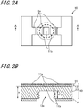
- Fig. 2A is a plan view schematically illustrating an example of a light emitting element mounting substrate according to the first embodiment
- Fig. 2B is a sectional view taken along line A-A' of the light emitting element mounting substrate in Fig. 2A
- a light emitting element mounting substrate 10 has a multilayer structure including an insulating layer 12 on a metal plate 13 and an electrode layer 11 on the insulating layer 12.
- a back side insulating layer 14 may be included under the metal plate 13.
- the insulating layer 12 is made of, for example, silicon nitride (Si 3 N 4 ) with 0.1 mm in thickness or aluminum nitride (AlN) with 0.3 mm in thickness.
- the material of the insulating layer 12 may be aluminum nitride.
- the back side insulating layer 14 may be disposed for preventing warp of the substrate 10. The material and thickness of the back side insulating layer 14 may be the same as those of the insulating layer 12.
- the electrode layer 11 includes a positive electrode 11a and a negative electrode 11b and is disposed with a pattern of copper or gold with, for example, 1 ⁇ m to 100 ⁇ m in thickness.
- the light emitting element is mounted on the electrode layer 11.
- the light emitting element mounting substrate 10 it is possible to more reliably transfer heat generated in the light emitting element to the outside through the bolt or the like screwed in the screw hole 13a of the metal plate 13.
- Fig. 3A is a plan view schematically illustrating an example of the light emitting module according to this embodiment
- Fig. 3B is a sectional view taken along line B-B' of the light emitting module in Fig. 3A
- the light emitting element mounting substrate 10 more specifically, metal plate 13
- a grease layer 60 may be included between the light emitting element mounting substrate 10 and the heatsink 40.
- the member fastening the metal plate 13 and the heatsink 40 is not limited to the bolt and may be "a full thread and a nut" functioning like the bolt.
- heat generated in the light emitting elements 20a to 20d passes through the electrode layer 11, the insulating layer 12, the metal plate 13, and the bolt 50 to be transferred to the heatsink 40.
- the heat conductivity of the metal plate 13 and the heat conductivity of the bolt 50 (or the full thread and the nut) are equal to each other, or when the heat conductivity of the metal plate 13 is smaller than the heat conductivity of the bolt 50, high heat-dissipation effect is realized.
- the material of both the metal plate 13 and the bolt 50 may be copper.
- a depth b of the screw hole 13a and a thickness a of the metal plate 13 illustrated in Fig. 2B may have the following relationships: 0.3 ⁇ a ⁇ b ⁇ 0.9 ⁇ a and 0.5 ⁇ a ⁇ b ⁇ 0.9 ⁇ a The above relationships may be determined based on the balance between the heat-dissipation efficiency and the intensity of the metal plate (consequently the intensity of the light emitting element mounting substrate).
- a gap of an air layer (hereinafter referred to as "gap") 15 is formed between a tip end of the bolt 50 screwed in the screw hole 13a of the metal plate 13 and a deepest portion 13b of the screw hole 13a (hereinafter referred to as “deepest portion of screw hole”) facing the tip end of the bolt 50, and the heat-dissipation effect is reduced in this portion.
- a metal joint is disposed in the gap 15 to suppress reduction of the heat-dissipation effect in the gap 15.
- Fig. 4A is a plan view schematically illustrating a light emitting module according to the second embodiment
- Fig. 4B is a sectional view taken along line C-C' of the light emitting module in Fig. 4A .
- a metal joint 70a is disposed in the gap 15 formed by the deepest portion 13b of the metal plate 13 and a tip end 50a of the bolt 50.
- the metal joint 70a may have (A) a hardness less than a hardness of the metal plate 13, or (B) a heat conductivity equal to or greater than a heat conductivity of the metal plate 13. There may be disposed a metal joint having (C) a hardness less than a hardness of the metal plate 13 and a heat conductivity equal to or greater than a heat conductivity of the metal plate 13.
- the material of the metal joint 70a when the material of the metal plate 13 is copper, the material of the metal joint 70a may be silver, gold, aluminum, solder, or the like for the example of (A).
- the material of the metal joint 70a may be silver or the like for the example of (B).
- the material of the metal joint 70a may be silver or the like for the example of (C).
- the material of the metal joint 70a when the material of the metal plate 13 is copper, the material of the metal joint 70a may be silver.
- FIG. 5A is a plan view schematically illustrating a light emitting module according to this embodiment
- Fig. 5B is a sectional view taken along line D-D' of the light emitting module in Fig. 5A .
- a metal joint 70b is disposed over an inner surface of the screw hole 13a of the metal plate 13 so as to surround the external thread of the bolt 50.
- the metal joint 70b is disposed to surround the entire inner surface of the screw hole 13a of the metal plate 13, and the gap 15 formed by the screw hole 13a of the metal plate 13 and the external thread of the bolt 50 is filled with the metal joint 70b. Accordingly, the heat generated in the light emitting elements 20a to 20d is reliably transferred to the bolt 50 through the metal plate 13.
- the material of the metal joint 70b in this embodiment may be determined similarly to determining the material of the metal joint 70a in the second embodiment.
- FIG. 6A is a plan view schematically illustrating a light emitting module according to a fourth embodiment
- Fig. 6B is a sectional view taken along line E-E' of the light emitting module in Fig. 6A .
- small holes 13c are formed in portions deeper than the deepest portion 13b of the metal plate 13, and these small holes 13c are filled with a metal joint 70c to increase the surface area in which the metal plate 13 and the metal joint contact with each other. Accordingly, the heat generated in the light emitting elements 20a to 20d is more reliably transferred to the bolt 50 through the metal plate 13.
- the material of the metal joint 70c in this embodiment may be determined similarly to determining the material of the metal joint 70a in the second embodiment.
- Fig. 7 is a plan view schematically illustrating a light emitting element mounted according to this embodiment.
- the multiple light emitting elements 20a to 20d may be disposed in a grid pattern on the electrode layer 11 including a positive electrode 11c and a negative electrode 11d.
- the center of the region in which the multiple light emitting elements 20a to 20d are mounted in the electrode layer 11 and the center of the bolt 50 coincide with each other. Accordingly, a light emitting module with an improved heat-dissipation effect is achieved with a balanced heat dissipation.
Landscapes
- Engineering & Computer Science (AREA)
- General Engineering & Computer Science (AREA)
- Physics & Mathematics (AREA)
- Thermal Sciences (AREA)
- Mechanical Engineering (AREA)
- Led Device Packages (AREA)
- Non-Portable Lighting Devices Or Systems Thereof (AREA)
Abstract
Description
- The present invention relates to a light emitting element mounting substrate, a light emitting device, and a light emitting module.
- Recently, light emitting elements such as a light emitting diode (LED), which consume smaller power and have better visibility than conventional light sources, have been employed as light sources of various light emitting devices (for example, a headlamp of automobile).
- The LED element has a characteristic of light emitting amount decreasing with an increase of temperature; thus, the increase of temperature has to be suppressed by taking measures to dissipate heat. In one of the measures taken typically, a substrate with the LED element mounted is fixed on a heatsink (also referred to as "heat-dissipation member" as well) to dissipate heat generated in the LED element to the heatsink. However, use of the heatsink alone is insufficient to obtain enough heat-dissipation effect. To address this, for example,
PTL 1 describes a technique for improving the heat-dissipation effect by disposing a grease layer between the substrate and the heatsink. There are needs of a light emitting element mounting substrate, a light emitting device, and a light emitting module having an improved heat-dissipation effect. - PTL 1: Japanese Unexamined Patent Application Publication No.
2014-120502 - A light emitting element mounting substrate of the present disclosure includes a metal plate, an insulating layer, and an electrode layer on which one or more light emitting elements are mountable, stacked in this order. The metal plate includes a bottomed screw hole opened at a surface opposite to a surface in contact with the insulating layer.
- A light emitting device of the present disclosure includes the light emitting element mounting substrate and one or more light emitting elements.
- A light emitting module of the present disclosure includes the light emitting device, a heatsink including a through-hole in a position corresponding to the bottomed screw hole, and a bolt screwed in the bottomed screw hole and fastening the heatsink and the metal plate, or a full thread and a nut for the fastening. A heat conductivity of the bolt or the full thread and the nut is equal to or greater than a heat conductivity of the metal plate.
- An object, feature, and advantage of the present disclosure will be more apparent with reference to the following detailed descriptions and drawings.
-
Fig. 1 is an overview schematically illustrating an example of a light emitting module according to a first embodiment. -
Fig. 2A is a plan view schematically illustrating an example of a light emitting element mounting substrate according to the first embodiment. -
Fig. 2B is a sectional view taken along line A-A' of the light emitting element mounting substrate inFig. 2A . -
Fig. 3A is a plan view schematically illustrating an example of the light emitting module according to the first embodiment. -
Fig. 3B is a sectional view taken along line B-B' of the light emitting module inFig. 3A . -
Fig. 4A is a plan view schematically illustrating an example of a light emitting module according to a second embodiment. -
Fig. 4B is a sectional view taken along line C-C' of the light emitting module inFig. 4A . -
Fig. 5A is a plan view schematically illustrating an example of a light emitting module according to a third embodiment. -
Fig. 5B is a sectional view taken along line D-D' of the light emitting module inFig. 5A . -
Fig. 6A is a plan view schematically illustrating an example of a light emitting module according to a fourth embodiment. -
Fig. 6B is a sectional view taken along line E-E' of the light emitting module inFig. 6A . -
Fig. 7 is a plan view schematically illustrating an example of a light emitting module according to a fifth embodiment. - Hereinafter, a light emitting element mounting substrate, a light emitting device, and a light emitting module according to the embodiments are described with reference to the accompanying drawings. In the following descriptions, top and bottom are differentiated by using words such as "top" or "on"; however, this is for convenience only and is not intended to restrict top and bottom in actually using the light emitting module and the like.
-
Fig. 1 is an external view schematically illustrating an example of a light emitting module according to this embodiment. Thelight emitting module 1 illustrated inFig. 1 is, for example, a member in a headlight of an automobile, in which alight emitting device 30 with alight emitting element 20 such as an LED mounted is disposed on aheatsink 40 for heat dissipation, and theheatsink 40 and thelight emitting device 30 are fixed to each other with a bolt or the like (not illustrated). Theheatsink 40 is a typical heatsink, and the material thereof is, for example, aluminum. Thelight emitting device 30 has a flat plate shape with, for example, 2 mm in length × 5 mm in width or 30 mm in length × 40 mm in width and about 4 to 6 mm in thickness. -
Fig. 1 illustrates an example of a light emitting module with four light emitting elements mounted; however, in this embodiment, the number of the light emitting elements is not limited to four, and one or more light emitting elements are mounted. Illustration of a power source, wiring, and the like of thelight emitting module 1 is omitted inFig. 1 . -
Fig. 2A is a plan view schematically illustrating an example of a light emitting element mounting substrate according to the first embodiment, andFig. 2B is a sectional view taken along line A-A' of the light emitting element mounting substrate inFig. 2A . As illustrated inFig. 2B , a light emittingelement mounting substrate 10 has a multilayer structure including aninsulating layer 12 on ametal plate 13 and anelectrode layer 11 on theinsulating layer 12. A backside insulating layer 14 may be included under themetal plate 13. - The
metal plate 13 is, for example, a copper plate with a thickness of 3 mm and 5 mm, inclusive, and includes ascrew hole 13a with internal threads (for example, ϕ = 3 mm) to be screwed with a later-described bolt (or full thread). - The
insulating layer 12 is made of, for example, silicon nitride (Si3N4) with 0.1 mm in thickness or aluminum nitride (AlN) with 0.3 mm in thickness. The material of the insulatinglayer 12 may be aluminum nitride. The backside insulating layer 14 may be disposed for preventing warp of thesubstrate 10. The material and thickness of the backside insulating layer 14 may be the same as those of the insulatinglayer 12. - The
electrode layer 11 includes apositive electrode 11a and anegative electrode 11b and is disposed with a pattern of copper or gold with, for example, 1 µm to 100 µm in thickness. The light emitting element is mounted on theelectrode layer 11. - According to the light emitting
element mounting substrate 10, it is possible to more reliably transfer heat generated in the light emitting element to the outside through the bolt or the like screwed in thescrew hole 13a of themetal plate 13. -
Fig. 3A is a plan view schematically illustrating an example of the light emitting module according to this embodiment, andFig. 3B is a sectional view taken along line B-B' of the light emitting module inFig. 3A . As illustrated inFig. 3B , in thelight emitting module 1,light emitting elements 20a to 20d are mounted on the light emittingelement mounting substrate 10, and the light emitting element mounting substrate 10 (more specifically, metal plate 13) and theheatsink 40 are fastened to each other by abolt 50. Agrease layer 60 may be included between the light emittingelement mounting substrate 10 and theheatsink 40. - The member fastening the
metal plate 13 and theheatsink 40 is not limited to the bolt and may be "a full thread and a nut" functioning like the bolt. - In a transparent plan view as illustrated in
Fig. 3A , when the center of the region in which the multiplelight emitting elements 20a to 20d are mounted in theelectrode layer 11 and the center of thebolt 50 coincide with each other, a light emitting module with an improved heat-dissipation effect is achieved with a balanced heat-dissipation. - As indicated by arrows in
Fig. 3B , heat generated in thelight emitting elements 20a to 20d passes through theelectrode layer 11, the insulatinglayer 12, themetal plate 13, and thebolt 50 to be transferred to theheatsink 40. When the heat conductivity of themetal plate 13 and the heat conductivity of the bolt 50 (or the full thread and the nut) are equal to each other, or when the heat conductivity of themetal plate 13 is smaller than the heat conductivity of thebolt 50, high heat-dissipation effect is realized. In the above-described example, the material of both themetal plate 13 and the bolt 50 (or the full thread and the nut) may be copper. - A depth b of the
screw hole 13a and a thickness a of themetal plate 13 illustrated inFig. 2B may have the following relationships:

- With the above-described light emitting module configuration, it is possible to more reliably transfer heat generated in the light emitting element to the heatsink through the metal plate and bolt.
- In the
light emitting module 1 according to the first embodiment, a gap of an air layer (hereinafter referred to as "gap") 15 is formed between a tip end of thebolt 50 screwed in thescrew hole 13a of themetal plate 13 and adeepest portion 13b of thescrew hole 13a (hereinafter referred to as "deepest portion of screw hole") facing the tip end of thebolt 50, and the heat-dissipation effect is reduced in this portion. Thus, in a second embodiment, a metal joint is disposed in thegap 15 to suppress reduction of the heat-dissipation effect in thegap 15. -
Fig. 4A is a plan view schematically illustrating a light emitting module according to the second embodiment, andFig. 4B is a sectional view taken along line C-C' of the light emitting module inFig. 4A . - As illustrated in
Fig. 4B , a metal joint 70a is disposed in thegap 15 formed by thedeepest portion 13b of themetal plate 13 and atip end 50a of thebolt 50. - The metal joint 70a may have (A) a hardness less than a hardness of the
metal plate 13, or (B) a heat conductivity equal to or greater than a heat conductivity of themetal plate 13. There may be disposed a metal joint having (C) a hardness less than a hardness of themetal plate 13 and a heat conductivity equal to or greater than a heat conductivity of themetal plate 13. - Specifically, for example, according to the values in Table 1, when the material of the
metal plate 13 is copper, the material of the metal joint 70a may be silver, gold, aluminum, solder, or the like for the example of (A). The material of the metal joint 70a may be silver or the like for the example of (B). The material of the metal joint 70a may be silver or the like for the example of (C). Thus, when the material of themetal plate 13 is copper, the material of the metal joint 70a may be silver. - As described above, since the reduction of the heat-dissipation effect in the
gap 15 is suppressed by disposing the metal joint 70a in thegap 15, it is possible to reliably transfer the heat generated in thelight emitting elements 20a to 20d to thebolt 50 and the like through themetal plate 13.[Table 1] hardness (Hv) heat conductivity [W/mK] copper 46 372 gold 26 295 silver 26 418 aluminum 25 204 solder (50Sn) 20 49 - This embodiment presents an example in which the same object as the second embodiment is achieved while a metal joint is disposed differently from the second embodiment.
Fig. 5A is a plan view schematically illustrating a light emitting module according to this embodiment, andFig. 5B is a sectional view taken along line D-D' of the light emitting module inFig. 5A . - As illustrated in
Fig. 5B , a metal joint 70b is disposed over an inner surface of thescrew hole 13a of themetal plate 13 so as to surround the external thread of thebolt 50. The metal joint 70b is disposed to surround the entire inner surface of thescrew hole 13a of themetal plate 13, and thegap 15 formed by thescrew hole 13a of themetal plate 13 and the external thread of thebolt 50 is filled with the metal joint 70b. Accordingly, the heat generated in thelight emitting elements 20a to 20d is reliably transferred to thebolt 50 through themetal plate 13. The material of the metal joint 70b in this embodiment may be determined similarly to determining the material of the metal joint 70a in the second embodiment. - This embodiment presents an example in which a metal joint is disposed to improve the heat-dissipation effect compared to the metal joint in the second embodiment.
Fig. 6A is a plan view schematically illustrating a light emitting module according to a fourth embodiment, andFig. 6B is a sectional view taken along line E-E' of the light emitting module inFig. 6A . - As illustrated in
Fig. 6B ,small holes 13c are formed in portions deeper than thedeepest portion 13b of themetal plate 13, and thesesmall holes 13c are filled with a metal joint 70c to increase the surface area in which themetal plate 13 and the metal joint contact with each other. Accordingly, the heat generated in thelight emitting elements 20a to 20d is more reliably transferred to thebolt 50 through themetal plate 13. The material of the metal joint 70c in this embodiment may be determined similarly to determining the material of the metal joint 70a in the second embodiment. -
Fig. 7 is a plan view schematically illustrating a light emitting element mounted according to this embodiment. As illustrated inFig. 7 , the multiplelight emitting elements 20a to 20d may be disposed in a grid pattern on theelectrode layer 11 including apositive electrode 11c and anegative electrode 11d. In this embodiment also, in the transparent plan view, the center of the region in which the multiplelight emitting elements 20a to 20d are mounted in theelectrode layer 11 and the center of thebolt 50 coincide with each other. Accordingly, a light emitting module with an improved heat-dissipation effect is achieved with a balanced heat dissipation. - The present disclosure can be implemented in other various aspects without departing from its sprit or the main feature. Thus, the above-described embodiments are merely examples at all respects, and the scope of the present disclosure is described in the claims and is never limited by the descriptions in the specification. All modifications and variations depending from the scope of claims are within the scope of the present disclosure.
-
- 1, 1a, 1b, 1c, 1d
- light emitting module
- 10
- light emitting element mounting substrate
- 11
- electrode layer
- 11a, 11c
- positive electrode
- 11b, 11d
- negative electrode
- 12
- insulating layer
- 13
- metal plate
- 13a
- screw hole
- 13b
- deepest portion
- 13c
- small hole
- 14
- back side insulating layer
- 15
- gap
- 20
- light emitting element
- 20a, 20b, 20c, 20d
- light emitting element
- 30
- light emitting device
- 40
- heatsink
- 50
- bolt
- 50a
- tip end of
bolt 50 - 60
- grease layer
- 70a, 70b, 70c
- metal joint
Claims (13)
- A light emitting element mounting substrate, comprising:a metal plate;an insulating layer; andan electrode layer on which one or more light emitting elements are mountable, the metal plate, the insulating layer, and the electrode layer being stacked in this order, whereinthe metal plate comprises a bottomed screw hole opened at a surface opposite to a surface in contact with the insulating layer.
- The light emitting element mounting substrate according to claim 1, wherein
in a transparent plan view, a region in which the one or more light emitting elements are mountable in the electrode layer at least partially overlaps with the bottomed screw hole of the metal plate. - The light emitting element mounting substrate according to claim 1 or 2, wherein
in a transparent plan view, a center of a region in which the one or more light emitting elements are mountable in the electrode layer coincides with a center of the bottomed screw hole of the metal plate. - The light emitting element mounting substrate according to any one of claims 1 to 3, wherein
a metal joint is disposed in a deepest portion of the bottomed screw hole of the metal plate, the metal joint having a hardness less than a hardness of the metal plate or a heat conductivity equal to or greater than a heat conductivity of the metal plate. - The light emitting element mounting substrate according to any one of claims 1 to 3, wherein
a metal joint is disposed in a deepest portion of the bottomed screw hole of the metal plate, the metal joint having a hardness less than a hardness of the metal plate and a heat conductivity equal to or greater than a heat conductivity of the metal plate. - The light emitting element mounting substrate according to claim 4 or 5, wherein
a material of the metal joint is solder, gold, silver, or aluminum. - The light emitting element mounting substrate according to claim 6, wherein
the metal joint is disposed over an entire inner surface of the bottomed screw hole. - The light emitting element mounting substrate according to claim 6, whereinthe metal plate comprises a small hole in a portion deeper than the deepest portion, andthe small hole is filled with the metal joint.
- The light emitting element mounting substrate according to any one of claims 1 to 8, wherein
a depth of the bottomed screw hole is 50% to 90%, inclusive, of a thickness of the metal plate. - A light emitting device, comprising:the light emitting element mounting substrate according to any one of claims 1 to 9; andone or more light emitting elements.
- A light emitting module, comprising:the light emitting device according to claim 10;a heatsink comprising a through-hole in a position corresponding to the bottomed screw hole; anda bolt screwed in the bottomed screw hole and fastening the heatsink and the metal plate, or a full thread and a nut screwed in the bottomed screw hole fastening the heatsink and the metal plate, whereina heat conductivity of the bolt or the full thread and the nut is equal to or greater than a heat conductivity of the metal plate.
- The light emitting module according to claim 11, further comprising:
a back side insulating layer between the metal plate and the heatsink, the back side insulating layer comprising a through-hole in a position corresponding to the bottomed screw hole. - The light emitting module according to claim 12, wherein
a material of the metal plate and the bolt or the full thread and the nut is copper,
a material of the metal joint is silver, and
a material of the back side insulating layer is Si3N4 or AlN.
Applications Claiming Priority (2)
| Application Number | Priority Date | Filing Date | Title |
|---|---|---|---|
| JP2016209100 | 2016-10-25 | ||
| PCT/JP2017/038498 WO2018079595A1 (en) | 2016-10-25 | 2017-10-25 | Light emitting element mounting substrate, light emitting device, and light emitting module |
Publications (3)
| Publication Number | Publication Date |
|---|---|
| EP3534060A1 true EP3534060A1 (en) | 2019-09-04 |
| EP3534060A4 EP3534060A4 (en) | 2020-07-01 |
| EP3534060B1 EP3534060B1 (en) | 2022-07-06 |
Family
ID=62025058
Family Applications (1)
| Application Number | Title | Priority Date | Filing Date |
|---|---|---|---|
| EP17863667.6A Active EP3534060B1 (en) | 2016-10-25 | 2017-10-25 | Light emitting element mounting substrate, light emitting device, and light emitting module |
Country Status (5)
| Country | Link |
|---|---|
| US (1) | US10985305B2 (en) |
| EP (1) | EP3534060B1 (en) |
| JP (1) | JP6677816B2 (en) |
| CN (1) | CN109863611B (en) |
| WO (1) | WO2018079595A1 (en) |
Families Citing this family (4)
| Publication number | Priority date | Publication date | Assignee | Title |
|---|---|---|---|---|
| JP6484982B2 (en) * | 2014-09-30 | 2019-03-20 | 日亜化学工業株式会社 | Method for manufacturing light emitting device |
| US10986722B1 (en) * | 2019-11-15 | 2021-04-20 | Goodrich Corporation | High performance heat sink for double sided printed circuit boards |
| US12068137B2 (en) * | 2020-09-25 | 2024-08-20 | Applied Materials, Inc. | Thread profiles for semiconductor process chamber components |
| KR102483766B1 (en) * | 2022-02-18 | 2023-01-03 | 주식회사 비와이티이씨 | LED lighting fixtures |
Family Cites Families (20)
| Publication number | Priority date | Publication date | Assignee | Title |
|---|---|---|---|---|
| EP1467414A4 (en) * | 2001-12-29 | 2007-07-11 | Hangzhou Fuyang Xinying Dianzi | A led and led lamp |
| TWM271255U (en) * | 2004-10-08 | 2005-07-21 | Bright Led Electronics Corp | High-power surface-mounted light-emitting diode with high heat dissipation property |
| JP4711715B2 (en) * | 2005-03-30 | 2011-06-29 | 株式会社東芝 | Semiconductor light emitting device and semiconductor light emitting unit |
| JP5303443B2 (en) * | 2009-12-07 | 2013-10-02 | 新電元工業株式会社 | Substrate lamination fixing structure and substrate lamination fixing method |
| JP5457851B2 (en) * | 2010-01-19 | 2014-04-02 | パナソニック株式会社 | lighting equipment |
| JP2011166001A (en) * | 2010-02-12 | 2011-08-25 | Oki Data Corp | Semiconductor device |
| US9583690B2 (en) * | 2010-04-07 | 2017-02-28 | Shenzhen Qin Bo Core Technology Development Co., Ltd. | LED lampwick, LED chip, and method for manufacturing LED chip |
| KR101077378B1 (en) * | 2010-06-23 | 2011-10-26 | 삼성전기주식회사 | Heat radiation board and its manufacturing method |
| TWI446602B (en) * | 2011-06-13 | 2014-07-21 | 旭德科技股份有限公司 | Package carrier board and package structure |
| JP5985846B2 (en) * | 2011-06-29 | 2016-09-06 | Flexceed株式会社 | Light-emitting element mounting substrate and LED package |
| KR101262917B1 (en) * | 2011-09-09 | 2013-05-09 | (주)포인트엔지니어링 | light emitting device array with heat sink and the manufacturing method thereof |
| JP5848976B2 (en) * | 2012-01-25 | 2016-01-27 | 新光電気工業株式会社 | WIRING BOARD, LIGHT EMITTING DEVICE, AND WIRING BOARD MANUFACTURING METHOD |
| JP2014075429A (en) * | 2012-10-03 | 2014-04-24 | Sharp Corp | Light emitting device and heat sink attachment method to the same |
| US20150276198A1 (en) * | 2012-10-19 | 2015-10-01 | Sharp Kabushiki Kaisha | Light-emitting apparatus and structure for attaching light-emitting apparatus to heat sink |
| JP6057161B2 (en) * | 2012-12-13 | 2017-01-11 | 東芝ライテック株式会社 | Light emitting device |
| JP6026315B2 (en) * | 2013-02-20 | 2016-11-16 | スタンレー電気株式会社 | Light emitting element module |
| CN103247742B (en) * | 2013-04-22 | 2015-12-09 | 广州有色金属研究院 | A kind of LED heat radiation substrate and manufacture method thereof |
| JP6604543B2 (en) * | 2013-08-09 | 2019-11-13 | 株式会社タムラ製作所 | Light emitting device |
| US9541273B2 (en) * | 2014-05-22 | 2017-01-10 | Wen-Sung Hu | Heat dissipation structure of SMD LED |
| CN205122643U (en) * | 2015-12-08 | 2016-03-30 | 上海策元实业有限公司 | Ceramic substrate LED cooling system based on room temperature liquid metal |
-
2017
- 2017-10-25 JP JP2018547713A patent/JP6677816B2/en active Active
- 2017-10-25 WO PCT/JP2017/038498 patent/WO2018079595A1/en not_active Ceased
- 2017-10-25 EP EP17863667.6A patent/EP3534060B1/en active Active
- 2017-10-25 CN CN201780064189.2A patent/CN109863611B/en active Active
- 2017-10-25 US US16/344,518 patent/US10985305B2/en not_active Expired - Fee Related
Also Published As
| Publication number | Publication date |
|---|---|
| US20190280179A1 (en) | 2019-09-12 |
| EP3534060B1 (en) | 2022-07-06 |
| US10985305B2 (en) | 2021-04-20 |
| JP6677816B2 (en) | 2020-04-08 |
| EP3534060A4 (en) | 2020-07-01 |
| JPWO2018079595A1 (en) | 2019-07-18 |
| WO2018079595A1 (en) | 2018-05-03 |
| CN109863611A (en) | 2019-06-07 |
| CN109863611B (en) | 2021-08-17 |
Similar Documents
| Publication | Publication Date | Title |
|---|---|---|
| US7804105B2 (en) | Side view type LED package | |
| EP3534060B1 (en) | Light emitting element mounting substrate, light emitting device, and light emitting module | |
| JP5919387B2 (en) | Light emitting device and structure for attaching light emitting device to heat sink | |
| US9702527B2 (en) | Light emitting device | |
| US7795635B2 (en) | Backlight unit equipped with light emitting diodes | |
| JP2004228387A (en) | Light emitting device | |
| EP2361005A1 (en) | Circuit module | |
| US7957146B2 (en) | Illumination device comprising a substrate plate and a heat sink | |
| US20100135034A1 (en) | Electronic component mounting module and electrical apparatus | |
| GB2429846A (en) | Heat sink | |
| CN101307893A (en) | Lighting device | |
| US6789609B2 (en) | Heat sink assembly structure | |
| DE202013102680U1 (en) | Full-angle luminaire with high cooling effect | |
| US20100301359A1 (en) | Light Emitting Diode Package Structure | |
| US11619368B2 (en) | Light-emitting module | |
| JP2011096416A (en) | Led lighting fixture | |
| JP4173527B2 (en) | Light emitting element mounting substrate and light emitting element module | |
| JP7192469B2 (en) | Mounting structure of insulated circuit board with heat sink to housing | |
| EP2294902A1 (en) | Cooling system for an led chip array | |
| JPH10189803A (en) | Mounting structure of insulating substrate for heat dissipating plate | |
| US11315842B2 (en) | Semiconductor package | |
| ES3054191T3 (en) | Heat sink structure and flexible light-emitting device having heat sink structure | |
| CN112786547B (en) | Thermal architecture | |
| KR200157207Y1 (en) | Heatsink | |
| KR20150028089A (en) | Heat sink |
Legal Events
| Date | Code | Title | Description |
|---|---|---|---|
| STAA | Information on the status of an ep patent application or granted ep patent |
Free format text: STATUS: THE INTERNATIONAL PUBLICATION HAS BEEN MADE |
|
| PUAI | Public reference made under article 153(3) epc to a published international application that has entered the european phase |
Free format text: ORIGINAL CODE: 0009012 |
|
| STAA | Information on the status of an ep patent application or granted ep patent |
Free format text: STATUS: REQUEST FOR EXAMINATION WAS MADE |
|
| 17P | Request for examination filed |
Effective date: 20190417 |
|
| AK | Designated contracting states |
Kind code of ref document: A1 Designated state(s): AL AT BE BG CH CY CZ DE DK EE ES FI FR GB GR HR HU IE IS IT LI LT LU LV MC MK MT NL NO PL PT RO RS SE SI SK SM TR |
|
| AX | Request for extension of the european patent |
Extension state: BA ME |
|
| DAV | Request for validation of the european patent (deleted) | ||
| DAX | Request for extension of the european patent (deleted) | ||
| A4 | Supplementary search report drawn up and despatched |
Effective date: 20200529 |
|
| RIC1 | Information provided on ipc code assigned before grant |
Ipc: H05K 1/05 20060101ALN20200525BHEP Ipc: F21S 41/00 20180101ALI20200525BHEP Ipc: H01L 33/64 20100101AFI20200525BHEP |
|
| REG | Reference to a national code |
Ref country code: DE Ref legal event code: R079 Ref document number: 602017059340 Country of ref document: DE Free format text: PREVIOUS MAIN CLASS: F21S0041000000 Ipc: H01L0033640000 |
|
| GRAP | Despatch of communication of intention to grant a patent |
Free format text: ORIGINAL CODE: EPIDOSNIGR1 |
|
| STAA | Information on the status of an ep patent application or granted ep patent |
Free format text: STATUS: GRANT OF PATENT IS INTENDED |
|
| RIC1 | Information provided on ipc code assigned before grant |
Ipc: H05K 1/05 20060101ALN20220120BHEP Ipc: F21S 41/00 20180101ALI20220120BHEP Ipc: H01L 33/64 20100101AFI20220120BHEP |
|
| INTG | Intention to grant announced |
Effective date: 20220207 |
|
| GRAS | Grant fee paid |
Free format text: ORIGINAL CODE: EPIDOSNIGR3 |
|
| GRAA | (expected) grant |
Free format text: ORIGINAL CODE: 0009210 |
|
| STAA | Information on the status of an ep patent application or granted ep patent |
Free format text: STATUS: THE PATENT HAS BEEN GRANTED |
|
| AK | Designated contracting states |
Kind code of ref document: B1 Designated state(s): AL AT BE BG CH CY CZ DE DK EE ES FI FR GB GR HR HU IE IS IT LI LT LU LV MC MK MT NL NO PL PT RO RS SE SI SK SM TR |
|
| REG | Reference to a national code |
Ref country code: AT Ref legal event code: REF Ref document number: 1503495 Country of ref document: AT Kind code of ref document: T Effective date: 20220715 Ref country code: CH Ref legal event code: EP |
|
| REG | Reference to a national code |
Ref country code: DE Ref legal event code: R096 Ref document number: 602017059340 Country of ref document: DE |
|
| REG | Reference to a national code |
Ref country code: IE Ref legal event code: FG4D |
|
| REG | Reference to a national code |
Ref country code: LT Ref legal event code: MG9D |
|
| REG | Reference to a national code |
Ref country code: NL Ref legal event code: MP Effective date: 20220706 |
|
| PG25 | Lapsed in a contracting state [announced via postgrant information from national office to epo] |
Ref country code: SE Free format text: LAPSE BECAUSE OF FAILURE TO SUBMIT A TRANSLATION OF THE DESCRIPTION OR TO PAY THE FEE WITHIN THE PRESCRIBED TIME-LIMIT Effective date: 20220706 Ref country code: RS Free format text: LAPSE BECAUSE OF FAILURE TO SUBMIT A TRANSLATION OF THE DESCRIPTION OR TO PAY THE FEE WITHIN THE PRESCRIBED TIME-LIMIT Effective date: 20220706 Ref country code: PT Free format text: LAPSE BECAUSE OF FAILURE TO SUBMIT A TRANSLATION OF THE DESCRIPTION OR TO PAY THE FEE WITHIN THE PRESCRIBED TIME-LIMIT Effective date: 20221107 Ref country code: NO Free format text: LAPSE BECAUSE OF FAILURE TO SUBMIT A TRANSLATION OF THE DESCRIPTION OR TO PAY THE FEE WITHIN THE PRESCRIBED TIME-LIMIT Effective date: 20221006 Ref country code: NL Free format text: LAPSE BECAUSE OF FAILURE TO SUBMIT A TRANSLATION OF THE DESCRIPTION OR TO PAY THE FEE WITHIN THE PRESCRIBED TIME-LIMIT Effective date: 20220706 Ref country code: LV Free format text: LAPSE BECAUSE OF FAILURE TO SUBMIT A TRANSLATION OF THE DESCRIPTION OR TO PAY THE FEE WITHIN THE PRESCRIBED TIME-LIMIT Effective date: 20220706 Ref country code: LT Free format text: LAPSE BECAUSE OF FAILURE TO SUBMIT A TRANSLATION OF THE DESCRIPTION OR TO PAY THE FEE WITHIN THE PRESCRIBED TIME-LIMIT Effective date: 20220706 Ref country code: FI Free format text: LAPSE BECAUSE OF FAILURE TO SUBMIT A TRANSLATION OF THE DESCRIPTION OR TO PAY THE FEE WITHIN THE PRESCRIBED TIME-LIMIT Effective date: 20220706 Ref country code: ES Free format text: LAPSE BECAUSE OF FAILURE TO SUBMIT A TRANSLATION OF THE DESCRIPTION OR TO PAY THE FEE WITHIN THE PRESCRIBED TIME-LIMIT Effective date: 20220706 |
|
| REG | Reference to a national code |
Ref country code: AT Ref legal event code: MK05 Ref document number: 1503495 Country of ref document: AT Kind code of ref document: T Effective date: 20220706 |
|
| PG25 | Lapsed in a contracting state [announced via postgrant information from national office to epo] |
Ref country code: PL Free format text: LAPSE BECAUSE OF FAILURE TO SUBMIT A TRANSLATION OF THE DESCRIPTION OR TO PAY THE FEE WITHIN THE PRESCRIBED TIME-LIMIT Effective date: 20220706 Ref country code: IS Free format text: LAPSE BECAUSE OF FAILURE TO SUBMIT A TRANSLATION OF THE DESCRIPTION OR TO PAY THE FEE WITHIN THE PRESCRIBED TIME-LIMIT Effective date: 20221106 Ref country code: HR Free format text: LAPSE BECAUSE OF FAILURE TO SUBMIT A TRANSLATION OF THE DESCRIPTION OR TO PAY THE FEE WITHIN THE PRESCRIBED TIME-LIMIT Effective date: 20220706 Ref country code: GR Free format text: LAPSE BECAUSE OF FAILURE TO SUBMIT A TRANSLATION OF THE DESCRIPTION OR TO PAY THE FEE WITHIN THE PRESCRIBED TIME-LIMIT Effective date: 20221007 |
|
| REG | Reference to a national code |
Ref country code: DE Ref legal event code: R097 Ref document number: 602017059340 Country of ref document: DE |
|
| PG25 | Lapsed in a contracting state [announced via postgrant information from national office to epo] |
Ref country code: SM Free format text: LAPSE BECAUSE OF FAILURE TO SUBMIT A TRANSLATION OF THE DESCRIPTION OR TO PAY THE FEE WITHIN THE PRESCRIBED TIME-LIMIT Effective date: 20220706 Ref country code: RO Free format text: LAPSE BECAUSE OF FAILURE TO SUBMIT A TRANSLATION OF THE DESCRIPTION OR TO PAY THE FEE WITHIN THE PRESCRIBED TIME-LIMIT Effective date: 20220706 Ref country code: DK Free format text: LAPSE BECAUSE OF FAILURE TO SUBMIT A TRANSLATION OF THE DESCRIPTION OR TO PAY THE FEE WITHIN THE PRESCRIBED TIME-LIMIT Effective date: 20220706 Ref country code: CZ Free format text: LAPSE BECAUSE OF FAILURE TO SUBMIT A TRANSLATION OF THE DESCRIPTION OR TO PAY THE FEE WITHIN THE PRESCRIBED TIME-LIMIT Effective date: 20220706 Ref country code: AT Free format text: LAPSE BECAUSE OF FAILURE TO SUBMIT A TRANSLATION OF THE DESCRIPTION OR TO PAY THE FEE WITHIN THE PRESCRIBED TIME-LIMIT Effective date: 20220706 |
|
| PLBE | No opposition filed within time limit |
Free format text: ORIGINAL CODE: 0009261 |
|
| STAA | Information on the status of an ep patent application or granted ep patent |
Free format text: STATUS: NO OPPOSITION FILED WITHIN TIME LIMIT |
|
| PG25 | Lapsed in a contracting state [announced via postgrant information from national office to epo] |
Ref country code: SK Free format text: LAPSE BECAUSE OF FAILURE TO SUBMIT A TRANSLATION OF THE DESCRIPTION OR TO PAY THE FEE WITHIN THE PRESCRIBED TIME-LIMIT Effective date: 20220706 Ref country code: MC Free format text: LAPSE BECAUSE OF FAILURE TO SUBMIT A TRANSLATION OF THE DESCRIPTION OR TO PAY THE FEE WITHIN THE PRESCRIBED TIME-LIMIT Effective date: 20220706 Ref country code: EE Free format text: LAPSE BECAUSE OF FAILURE TO SUBMIT A TRANSLATION OF THE DESCRIPTION OR TO PAY THE FEE WITHIN THE PRESCRIBED TIME-LIMIT Effective date: 20220706 |
|
| REG | Reference to a national code |
Ref country code: CH Ref legal event code: PL |
|
| 26N | No opposition filed |
Effective date: 20230411 |
|
| P01 | Opt-out of the competence of the unified patent court (upc) registered |
Effective date: 20230508 |
|
| REG | Reference to a national code |
Ref country code: BE Ref legal event code: MM Effective date: 20221031 |
|
| PG25 | Lapsed in a contracting state [announced via postgrant information from national office to epo] |
Ref country code: LU Free format text: LAPSE BECAUSE OF NON-PAYMENT OF DUE FEES Effective date: 20221025 Ref country code: AL Free format text: LAPSE BECAUSE OF FAILURE TO SUBMIT A TRANSLATION OF THE DESCRIPTION OR TO PAY THE FEE WITHIN THE PRESCRIBED TIME-LIMIT Effective date: 20220706 |
|
| PG25 | Lapsed in a contracting state [announced via postgrant information from national office to epo] |
Ref country code: LI Free format text: LAPSE BECAUSE OF NON-PAYMENT OF DUE FEES Effective date: 20221031 Ref country code: FR Free format text: LAPSE BECAUSE OF NON-PAYMENT OF DUE FEES Effective date: 20221031 Ref country code: CH Free format text: LAPSE BECAUSE OF NON-PAYMENT OF DUE FEES Effective date: 20221031 |
|
| PG25 | Lapsed in a contracting state [announced via postgrant information from national office to epo] |
Ref country code: SI Free format text: LAPSE BECAUSE OF FAILURE TO SUBMIT A TRANSLATION OF THE DESCRIPTION OR TO PAY THE FEE WITHIN THE PRESCRIBED TIME-LIMIT Effective date: 20220706 |
|
| PG25 | Lapsed in a contracting state [announced via postgrant information from national office to epo] |
Ref country code: BE Free format text: LAPSE BECAUSE OF NON-PAYMENT OF DUE FEES Effective date: 20221031 |
|
| PG25 | Lapsed in a contracting state [announced via postgrant information from national office to epo] |
Ref country code: IE Free format text: LAPSE BECAUSE OF NON-PAYMENT OF DUE FEES Effective date: 20221025 |
|
| PG25 | Lapsed in a contracting state [announced via postgrant information from national office to epo] |
Ref country code: IT Free format text: LAPSE BECAUSE OF FAILURE TO SUBMIT A TRANSLATION OF THE DESCRIPTION OR TO PAY THE FEE WITHIN THE PRESCRIBED TIME-LIMIT Effective date: 20220706 |
|
| PG25 | Lapsed in a contracting state [announced via postgrant information from national office to epo] |
Ref country code: HU Free format text: LAPSE BECAUSE OF FAILURE TO SUBMIT A TRANSLATION OF THE DESCRIPTION OR TO PAY THE FEE WITHIN THE PRESCRIBED TIME-LIMIT; INVALID AB INITIO Effective date: 20171025 |
|
| PG25 | Lapsed in a contracting state [announced via postgrant information from national office to epo] |
Ref country code: CY Free format text: LAPSE BECAUSE OF FAILURE TO SUBMIT A TRANSLATION OF THE DESCRIPTION OR TO PAY THE FEE WITHIN THE PRESCRIBED TIME-LIMIT Effective date: 20220706 |
|
| PG25 | Lapsed in a contracting state [announced via postgrant information from national office to epo] |
Ref country code: MK Free format text: LAPSE BECAUSE OF FAILURE TO SUBMIT A TRANSLATION OF THE DESCRIPTION OR TO PAY THE FEE WITHIN THE PRESCRIBED TIME-LIMIT Effective date: 20220706 |
|
| PG25 | Lapsed in a contracting state [announced via postgrant information from national office to epo] |
Ref country code: BG Free format text: LAPSE BECAUSE OF FAILURE TO SUBMIT A TRANSLATION OF THE DESCRIPTION OR TO PAY THE FEE WITHIN THE PRESCRIBED TIME-LIMIT Effective date: 20220706 |
|
| PG25 | Lapsed in a contracting state [announced via postgrant information from national office to epo] |
Ref country code: MT Free format text: LAPSE BECAUSE OF FAILURE TO SUBMIT A TRANSLATION OF THE DESCRIPTION OR TO PAY THE FEE WITHIN THE PRESCRIBED TIME-LIMIT Effective date: 20220706 |
|
| PGFP | Annual fee paid to national office [announced via postgrant information from national office to epo] |
Ref country code: GB Payment date: 20240905 Year of fee payment: 8 |
|
| REG | Reference to a national code |
Ref country code: DE Ref legal event code: R079 Ref document number: 602017059340 Country of ref document: DE Free format text: PREVIOUS MAIN CLASS: H01L0033640000 Ipc: H10H0020858000 |
|
| PGFP | Annual fee paid to national office [announced via postgrant information from national office to epo] |
Ref country code: DE Payment date: 20240828 Year of fee payment: 8 |
|
| PG25 | Lapsed in a contracting state [announced via postgrant information from national office to epo] |
Ref country code: TR Free format text: LAPSE BECAUSE OF FAILURE TO SUBMIT A TRANSLATION OF THE DESCRIPTION OR TO PAY THE FEE WITHIN THE PRESCRIBED TIME-LIMIT Effective date: 20220706 |