EP3533902A1 - Grain-oriented electrical steel sheet and production method for grain-oriented electrical steel sheet - Google Patents
Grain-oriented electrical steel sheet and production method for grain-oriented electrical steel sheet Download PDFInfo
- Publication number
- EP3533902A1 EP3533902A1 EP17885024.4A EP17885024A EP3533902A1 EP 3533902 A1 EP3533902 A1 EP 3533902A1 EP 17885024 A EP17885024 A EP 17885024A EP 3533902 A1 EP3533902 A1 EP 3533902A1
- Authority
- EP
- European Patent Office
- Prior art keywords
- coating
- steel sheet
- oriented electrical
- electrical steel
- grain oriented
- Prior art date
- Legal status (The legal status is an assumption and is not a legal conclusion. Google has not performed a legal analysis and makes no representation as to the accuracy of the status listed.)
- Granted
Links
Images
Classifications
-
- C—CHEMISTRY; METALLURGY
- C23—COATING METALLIC MATERIAL; COATING MATERIAL WITH METALLIC MATERIAL; CHEMICAL SURFACE TREATMENT; DIFFUSION TREATMENT OF METALLIC MATERIAL; COATING BY VACUUM EVAPORATION, BY SPUTTERING, BY ION IMPLANTATION OR BY CHEMICAL VAPOUR DEPOSITION, IN GENERAL; INHIBITING CORROSION OF METALLIC MATERIAL OR INCRUSTATION IN GENERAL
- C23C—COATING METALLIC MATERIAL; COATING MATERIAL WITH METALLIC MATERIAL; SURFACE TREATMENT OF METALLIC MATERIAL BY DIFFUSION INTO THE SURFACE, BY CHEMICAL CONVERSION OR SUBSTITUTION; COATING BY VACUUM EVAPORATION, BY SPUTTERING, BY ION IMPLANTATION OR BY CHEMICAL VAPOUR DEPOSITION, IN GENERAL
- C23C28/00—Coating for obtaining at least two superposed coatings either by methods not provided for in a single one of groups C23C2/00 - C23C26/00 or by combinations of methods provided for in subclasses C23C and C25C or C25D
- C23C28/04—Coating for obtaining at least two superposed coatings either by methods not provided for in a single one of groups C23C2/00 - C23C26/00 or by combinations of methods provided for in subclasses C23C and C25C or C25D only coatings of inorganic non-metallic material
-
- C—CHEMISTRY; METALLURGY
- C23—COATING METALLIC MATERIAL; COATING MATERIAL WITH METALLIC MATERIAL; CHEMICAL SURFACE TREATMENT; DIFFUSION TREATMENT OF METALLIC MATERIAL; COATING BY VACUUM EVAPORATION, BY SPUTTERING, BY ION IMPLANTATION OR BY CHEMICAL VAPOUR DEPOSITION, IN GENERAL; INHIBITING CORROSION OF METALLIC MATERIAL OR INCRUSTATION IN GENERAL
- C23C—COATING METALLIC MATERIAL; COATING MATERIAL WITH METALLIC MATERIAL; SURFACE TREATMENT OF METALLIC MATERIAL BY DIFFUSION INTO THE SURFACE, BY CHEMICAL CONVERSION OR SUBSTITUTION; COATING BY VACUUM EVAPORATION, BY SPUTTERING, BY ION IMPLANTATION OR BY CHEMICAL VAPOUR DEPOSITION, IN GENERAL
- C23C22/00—Chemical surface treatment of metallic material by reaction of the surface with a reactive liquid, leaving reaction products of surface material in the coating, e.g. conversion coatings, passivation of metals
- C23C22/05—Chemical surface treatment of metallic material by reaction of the surface with a reactive liquid, leaving reaction products of surface material in the coating, e.g. conversion coatings, passivation of metals using aqueous solutions
- C23C22/06—Chemical surface treatment of metallic material by reaction of the surface with a reactive liquid, leaving reaction products of surface material in the coating, e.g. conversion coatings, passivation of metals using aqueous solutions using aqueous acidic solutions with pH less than 6
- C23C22/07—Chemical surface treatment of metallic material by reaction of the surface with a reactive liquid, leaving reaction products of surface material in the coating, e.g. conversion coatings, passivation of metals using aqueous solutions using aqueous acidic solutions with pH less than 6 containing phosphates
- C23C22/08—Orthophosphates
-
- C—CHEMISTRY; METALLURGY
- C21—METALLURGY OF IRON
- C21D—MODIFYING THE PHYSICAL STRUCTURE OF FERROUS METALS; GENERAL DEVICES FOR HEAT TREATMENT OF FERROUS OR NON-FERROUS METALS OR ALLOYS; MAKING METAL MALLEABLE, e.g. BY DECARBURISATION OR TEMPERING
- C21D8/00—Modifying the physical properties of ferrous metals or ferrous alloys by deformation combined with, or followed by, heat treatment
- C21D8/12—Modifying the physical properties of ferrous metals or ferrous alloys by deformation combined with, or followed by, heat treatment during manufacturing of articles with special electromagnetic properties
-
- C—CHEMISTRY; METALLURGY
- C21—METALLURGY OF IRON
- C21D—MODIFYING THE PHYSICAL STRUCTURE OF FERROUS METALS; GENERAL DEVICES FOR HEAT TREATMENT OF FERROUS OR NON-FERROUS METALS OR ALLOYS; MAKING METAL MALLEABLE, e.g. BY DECARBURISATION OR TEMPERING
- C21D9/00—Heat treatment, e.g. annealing, hardening, quenching or tempering, adapted for particular articles; Furnaces therefor
- C21D9/46—Heat treatment, e.g. annealing, hardening, quenching or tempering, adapted for particular articles; Furnaces therefor for sheet metals
-
- C—CHEMISTRY; METALLURGY
- C22—METALLURGY; FERROUS OR NON-FERROUS ALLOYS; TREATMENT OF ALLOYS OR NON-FERROUS METALS
- C22C—ALLOYS
- C22C38/00—Ferrous alloys, e.g. steel alloys
-
- C—CHEMISTRY; METALLURGY
- C22—METALLURGY; FERROUS OR NON-FERROUS ALLOYS; TREATMENT OF ALLOYS OR NON-FERROUS METALS
- C22C—ALLOYS
- C22C38/00—Ferrous alloys, e.g. steel alloys
- C22C38/001—Ferrous alloys, e.g. steel alloys containing N
-
- C—CHEMISTRY; METALLURGY
- C22—METALLURGY; FERROUS OR NON-FERROUS ALLOYS; TREATMENT OF ALLOYS OR NON-FERROUS METALS
- C22C—ALLOYS
- C22C38/00—Ferrous alloys, e.g. steel alloys
- C22C38/02—Ferrous alloys, e.g. steel alloys containing silicon
-
- C—CHEMISTRY; METALLURGY
- C22—METALLURGY; FERROUS OR NON-FERROUS ALLOYS; TREATMENT OF ALLOYS OR NON-FERROUS METALS
- C22C—ALLOYS
- C22C38/00—Ferrous alloys, e.g. steel alloys
- C22C38/04—Ferrous alloys, e.g. steel alloys containing manganese
-
- C—CHEMISTRY; METALLURGY
- C22—METALLURGY; FERROUS OR NON-FERROUS ALLOYS; TREATMENT OF ALLOYS OR NON-FERROUS METALS
- C22C—ALLOYS
- C22C38/00—Ferrous alloys, e.g. steel alloys
- C22C38/06—Ferrous alloys, e.g. steel alloys containing aluminium
-
- C—CHEMISTRY; METALLURGY
- C22—METALLURGY; FERROUS OR NON-FERROUS ALLOYS; TREATMENT OF ALLOYS OR NON-FERROUS METALS
- C22C—ALLOYS
- C22C38/00—Ferrous alloys, e.g. steel alloys
- C22C38/60—Ferrous alloys, e.g. steel alloys containing lead, selenium, tellurium, or antimony, or more than 0.04% by weight of sulfur
-
- C—CHEMISTRY; METALLURGY
- C23—COATING METALLIC MATERIAL; COATING MATERIAL WITH METALLIC MATERIAL; CHEMICAL SURFACE TREATMENT; DIFFUSION TREATMENT OF METALLIC MATERIAL; COATING BY VACUUM EVAPORATION, BY SPUTTERING, BY ION IMPLANTATION OR BY CHEMICAL VAPOUR DEPOSITION, IN GENERAL; INHIBITING CORROSION OF METALLIC MATERIAL OR INCRUSTATION IN GENERAL
- C23C—COATING METALLIC MATERIAL; COATING MATERIAL WITH METALLIC MATERIAL; SURFACE TREATMENT OF METALLIC MATERIAL BY DIFFUSION INTO THE SURFACE, BY CHEMICAL CONVERSION OR SUBSTITUTION; COATING BY VACUUM EVAPORATION, BY SPUTTERING, BY ION IMPLANTATION OR BY CHEMICAL VAPOUR DEPOSITION, IN GENERAL
- C23C14/00—Coating by vacuum evaporation, by sputtering or by ion implantation of the coating forming material
- C23C14/06—Coating by vacuum evaporation, by sputtering or by ion implantation of the coating forming material characterised by the coating material
-
- C—CHEMISTRY; METALLURGY
- C23—COATING METALLIC MATERIAL; COATING MATERIAL WITH METALLIC MATERIAL; CHEMICAL SURFACE TREATMENT; DIFFUSION TREATMENT OF METALLIC MATERIAL; COATING BY VACUUM EVAPORATION, BY SPUTTERING, BY ION IMPLANTATION OR BY CHEMICAL VAPOUR DEPOSITION, IN GENERAL; INHIBITING CORROSION OF METALLIC MATERIAL OR INCRUSTATION IN GENERAL
- C23C—COATING METALLIC MATERIAL; COATING MATERIAL WITH METALLIC MATERIAL; SURFACE TREATMENT OF METALLIC MATERIAL BY DIFFUSION INTO THE SURFACE, BY CHEMICAL CONVERSION OR SUBSTITUTION; COATING BY VACUUM EVAPORATION, BY SPUTTERING, BY ION IMPLANTATION OR BY CHEMICAL VAPOUR DEPOSITION, IN GENERAL
- C23C14/00—Coating by vacuum evaporation, by sputtering or by ion implantation of the coating forming material
- C23C14/06—Coating by vacuum evaporation, by sputtering or by ion implantation of the coating forming material characterised by the coating material
- C23C14/0641—Nitrides
-
- C—CHEMISTRY; METALLURGY
- C23—COATING METALLIC MATERIAL; COATING MATERIAL WITH METALLIC MATERIAL; CHEMICAL SURFACE TREATMENT; DIFFUSION TREATMENT OF METALLIC MATERIAL; COATING BY VACUUM EVAPORATION, BY SPUTTERING, BY ION IMPLANTATION OR BY CHEMICAL VAPOUR DEPOSITION, IN GENERAL; INHIBITING CORROSION OF METALLIC MATERIAL OR INCRUSTATION IN GENERAL
- C23C—COATING METALLIC MATERIAL; COATING MATERIAL WITH METALLIC MATERIAL; SURFACE TREATMENT OF METALLIC MATERIAL BY DIFFUSION INTO THE SURFACE, BY CHEMICAL CONVERSION OR SUBSTITUTION; COATING BY VACUUM EVAPORATION, BY SPUTTERING, BY ION IMPLANTATION OR BY CHEMICAL VAPOUR DEPOSITION, IN GENERAL
- C23C14/00—Coating by vacuum evaporation, by sputtering or by ion implantation of the coating forming material
- C23C14/06—Coating by vacuum evaporation, by sputtering or by ion implantation of the coating forming material characterised by the coating material
- C23C14/0664—Carbonitrides
-
- C—CHEMISTRY; METALLURGY
- C23—COATING METALLIC MATERIAL; COATING MATERIAL WITH METALLIC MATERIAL; CHEMICAL SURFACE TREATMENT; DIFFUSION TREATMENT OF METALLIC MATERIAL; COATING BY VACUUM EVAPORATION, BY SPUTTERING, BY ION IMPLANTATION OR BY CHEMICAL VAPOUR DEPOSITION, IN GENERAL; INHIBITING CORROSION OF METALLIC MATERIAL OR INCRUSTATION IN GENERAL
- C23C—COATING METALLIC MATERIAL; COATING MATERIAL WITH METALLIC MATERIAL; SURFACE TREATMENT OF METALLIC MATERIAL BY DIFFUSION INTO THE SURFACE, BY CHEMICAL CONVERSION OR SUBSTITUTION; COATING BY VACUUM EVAPORATION, BY SPUTTERING, BY ION IMPLANTATION OR BY CHEMICAL VAPOUR DEPOSITION, IN GENERAL
- C23C16/00—Chemical coating by decomposition of gaseous compounds, without leaving reaction products of surface material in the coating, i.e. chemical vapour deposition [CVD] processes
- C23C16/22—Chemical coating by decomposition of gaseous compounds, without leaving reaction products of surface material in the coating, i.e. chemical vapour deposition [CVD] processes characterised by the deposition of inorganic material, other than metallic material
- C23C16/30—Deposition of compounds, mixtures or solid solutions, e.g. borides, carbides, nitrides
- C23C16/34—Nitrides
-
- C—CHEMISTRY; METALLURGY
- C23—COATING METALLIC MATERIAL; COATING MATERIAL WITH METALLIC MATERIAL; CHEMICAL SURFACE TREATMENT; DIFFUSION TREATMENT OF METALLIC MATERIAL; COATING BY VACUUM EVAPORATION, BY SPUTTERING, BY ION IMPLANTATION OR BY CHEMICAL VAPOUR DEPOSITION, IN GENERAL; INHIBITING CORROSION OF METALLIC MATERIAL OR INCRUSTATION IN GENERAL
- C23C—COATING METALLIC MATERIAL; COATING MATERIAL WITH METALLIC MATERIAL; SURFACE TREATMENT OF METALLIC MATERIAL BY DIFFUSION INTO THE SURFACE, BY CHEMICAL CONVERSION OR SUBSTITUTION; COATING BY VACUUM EVAPORATION, BY SPUTTERING, BY ION IMPLANTATION OR BY CHEMICAL VAPOUR DEPOSITION, IN GENERAL
- C23C16/00—Chemical coating by decomposition of gaseous compounds, without leaving reaction products of surface material in the coating, i.e. chemical vapour deposition [CVD] processes
- C23C16/22—Chemical coating by decomposition of gaseous compounds, without leaving reaction products of surface material in the coating, i.e. chemical vapour deposition [CVD] processes characterised by the deposition of inorganic material, other than metallic material
- C23C16/30—Deposition of compounds, mixtures or solid solutions, e.g. borides, carbides, nitrides
- C23C16/36—Carbonitrides
-
- C—CHEMISTRY; METALLURGY
- C23—COATING METALLIC MATERIAL; COATING MATERIAL WITH METALLIC MATERIAL; CHEMICAL SURFACE TREATMENT; DIFFUSION TREATMENT OF METALLIC MATERIAL; COATING BY VACUUM EVAPORATION, BY SPUTTERING, BY ION IMPLANTATION OR BY CHEMICAL VAPOUR DEPOSITION, IN GENERAL; INHIBITING CORROSION OF METALLIC MATERIAL OR INCRUSTATION IN GENERAL
- C23C—COATING METALLIC MATERIAL; COATING MATERIAL WITH METALLIC MATERIAL; SURFACE TREATMENT OF METALLIC MATERIAL BY DIFFUSION INTO THE SURFACE, BY CHEMICAL CONVERSION OR SUBSTITUTION; COATING BY VACUUM EVAPORATION, BY SPUTTERING, BY ION IMPLANTATION OR BY CHEMICAL VAPOUR DEPOSITION, IN GENERAL
- C23C22/00—Chemical surface treatment of metallic material by reaction of the surface with a reactive liquid, leaving reaction products of surface material in the coating, e.g. conversion coatings, passivation of metals
-
- C—CHEMISTRY; METALLURGY
- C23—COATING METALLIC MATERIAL; COATING MATERIAL WITH METALLIC MATERIAL; CHEMICAL SURFACE TREATMENT; DIFFUSION TREATMENT OF METALLIC MATERIAL; COATING BY VACUUM EVAPORATION, BY SPUTTERING, BY ION IMPLANTATION OR BY CHEMICAL VAPOUR DEPOSITION, IN GENERAL; INHIBITING CORROSION OF METALLIC MATERIAL OR INCRUSTATION IN GENERAL
- C23C—COATING METALLIC MATERIAL; COATING MATERIAL WITH METALLIC MATERIAL; SURFACE TREATMENT OF METALLIC MATERIAL BY DIFFUSION INTO THE SURFACE, BY CHEMICAL CONVERSION OR SUBSTITUTION; COATING BY VACUUM EVAPORATION, BY SPUTTERING, BY ION IMPLANTATION OR BY CHEMICAL VAPOUR DEPOSITION, IN GENERAL
- C23C22/00—Chemical surface treatment of metallic material by reaction of the surface with a reactive liquid, leaving reaction products of surface material in the coating, e.g. conversion coatings, passivation of metals
- C23C22/05—Chemical surface treatment of metallic material by reaction of the surface with a reactive liquid, leaving reaction products of surface material in the coating, e.g. conversion coatings, passivation of metals using aqueous solutions
- C23C22/06—Chemical surface treatment of metallic material by reaction of the surface with a reactive liquid, leaving reaction products of surface material in the coating, e.g. conversion coatings, passivation of metals using aqueous solutions using aqueous acidic solutions with pH less than 6
- C23C22/07—Chemical surface treatment of metallic material by reaction of the surface with a reactive liquid, leaving reaction products of surface material in the coating, e.g. conversion coatings, passivation of metals using aqueous solutions using aqueous acidic solutions with pH less than 6 containing phosphates
-
- C—CHEMISTRY; METALLURGY
- C23—COATING METALLIC MATERIAL; COATING MATERIAL WITH METALLIC MATERIAL; CHEMICAL SURFACE TREATMENT; DIFFUSION TREATMENT OF METALLIC MATERIAL; COATING BY VACUUM EVAPORATION, BY SPUTTERING, BY ION IMPLANTATION OR BY CHEMICAL VAPOUR DEPOSITION, IN GENERAL; INHIBITING CORROSION OF METALLIC MATERIAL OR INCRUSTATION IN GENERAL
- C23C—COATING METALLIC MATERIAL; COATING MATERIAL WITH METALLIC MATERIAL; SURFACE TREATMENT OF METALLIC MATERIAL BY DIFFUSION INTO THE SURFACE, BY CHEMICAL CONVERSION OR SUBSTITUTION; COATING BY VACUUM EVAPORATION, BY SPUTTERING, BY ION IMPLANTATION OR BY CHEMICAL VAPOUR DEPOSITION, IN GENERAL
- C23C22/00—Chemical surface treatment of metallic material by reaction of the surface with a reactive liquid, leaving reaction products of surface material in the coating, e.g. conversion coatings, passivation of metals
- C23C22/73—Chemical surface treatment of metallic material by reaction of the surface with a reactive liquid, leaving reaction products of surface material in the coating, e.g. conversion coatings, passivation of metals characterised by the process
- C23C22/74—Chemical surface treatment of metallic material by reaction of the surface with a reactive liquid, leaving reaction products of surface material in the coating, e.g. conversion coatings, passivation of metals characterised by the process for obtaining burned-in conversion coatings
-
- C—CHEMISTRY; METALLURGY
- C23—COATING METALLIC MATERIAL; COATING MATERIAL WITH METALLIC MATERIAL; CHEMICAL SURFACE TREATMENT; DIFFUSION TREATMENT OF METALLIC MATERIAL; COATING BY VACUUM EVAPORATION, BY SPUTTERING, BY ION IMPLANTATION OR BY CHEMICAL VAPOUR DEPOSITION, IN GENERAL; INHIBITING CORROSION OF METALLIC MATERIAL OR INCRUSTATION IN GENERAL
- C23C—COATING METALLIC MATERIAL; COATING MATERIAL WITH METALLIC MATERIAL; SURFACE TREATMENT OF METALLIC MATERIAL BY DIFFUSION INTO THE SURFACE, BY CHEMICAL CONVERSION OR SUBSTITUTION; COATING BY VACUUM EVAPORATION, BY SPUTTERING, BY ION IMPLANTATION OR BY CHEMICAL VAPOUR DEPOSITION, IN GENERAL
- C23C22/00—Chemical surface treatment of metallic material by reaction of the surface with a reactive liquid, leaving reaction products of surface material in the coating, e.g. conversion coatings, passivation of metals
- C23C22/82—After-treatment
-
- H—ELECTRICITY
- H01—ELECTRIC ELEMENTS
- H01F—MAGNETS; INDUCTANCES; TRANSFORMERS; SELECTION OF MATERIALS FOR THEIR MAGNETIC PROPERTIES
- H01F1/00—Magnets or magnetic bodies characterised by the magnetic materials therefor; Selection of materials for their magnetic properties
- H01F1/01—Magnets or magnetic bodies characterised by the magnetic materials therefor; Selection of materials for their magnetic properties of inorganic materials
- H01F1/03—Magnets or magnetic bodies characterised by the magnetic materials therefor; Selection of materials for their magnetic properties of inorganic materials characterised by their coercivity
- H01F1/12—Magnets or magnetic bodies characterised by the magnetic materials therefor; Selection of materials for their magnetic properties of inorganic materials characterised by their coercivity of soft-magnetic materials
- H01F1/14—Magnets or magnetic bodies characterised by the magnetic materials therefor; Selection of materials for their magnetic properties of inorganic materials characterised by their coercivity of soft-magnetic materials metals or alloys
- H01F1/147—Alloys characterised by their composition
-
- H—ELECTRICITY
- H01—ELECTRIC ELEMENTS
- H01F—MAGNETS; INDUCTANCES; TRANSFORMERS; SELECTION OF MATERIALS FOR THEIR MAGNETIC PROPERTIES
- H01F1/00—Magnets or magnetic bodies characterised by the magnetic materials therefor; Selection of materials for their magnetic properties
- H01F1/01—Magnets or magnetic bodies characterised by the magnetic materials therefor; Selection of materials for their magnetic properties of inorganic materials
- H01F1/03—Magnets or magnetic bodies characterised by the magnetic materials therefor; Selection of materials for their magnetic properties of inorganic materials characterised by their coercivity
- H01F1/12—Magnets or magnetic bodies characterised by the magnetic materials therefor; Selection of materials for their magnetic properties of inorganic materials characterised by their coercivity of soft-magnetic materials
- H01F1/14—Magnets or magnetic bodies characterised by the magnetic materials therefor; Selection of materials for their magnetic properties of inorganic materials characterised by their coercivity of soft-magnetic materials metals or alloys
- H01F1/16—Magnets or magnetic bodies characterised by the magnetic materials therefor; Selection of materials for their magnetic properties of inorganic materials characterised by their coercivity of soft-magnetic materials metals or alloys in the form of sheets
-
- H—ELECTRICITY
- H01—ELECTRIC ELEMENTS
- H01F—MAGNETS; INDUCTANCES; TRANSFORMERS; SELECTION OF MATERIALS FOR THEIR MAGNETIC PROPERTIES
- H01F1/00—Magnets or magnetic bodies characterised by the magnetic materials therefor; Selection of materials for their magnetic properties
- H01F1/01—Magnets or magnetic bodies characterised by the magnetic materials therefor; Selection of materials for their magnetic properties of inorganic materials
- H01F1/03—Magnets or magnetic bodies characterised by the magnetic materials therefor; Selection of materials for their magnetic properties of inorganic materials characterised by their coercivity
- H01F1/12—Magnets or magnetic bodies characterised by the magnetic materials therefor; Selection of materials for their magnetic properties of inorganic materials characterised by their coercivity of soft-magnetic materials
- H01F1/14—Magnets or magnetic bodies characterised by the magnetic materials therefor; Selection of materials for their magnetic properties of inorganic materials characterised by their coercivity of soft-magnetic materials metals or alloys
- H01F1/16—Magnets or magnetic bodies characterised by the magnetic materials therefor; Selection of materials for their magnetic properties of inorganic materials characterised by their coercivity of soft-magnetic materials metals or alloys in the form of sheets
- H01F1/18—Magnets or magnetic bodies characterised by the magnetic materials therefor; Selection of materials for their magnetic properties of inorganic materials characterised by their coercivity of soft-magnetic materials metals or alloys in the form of sheets with insulating coating
Definitions
- the present invention relates to a grain oriented electrical steel sheet and a producing method of a grain oriented electrical steel sheet.
- Grain oriented electrical steel sheets are soft magnetic materials used as materials for iron cores of transformers, generators and the like. Grain oriented electrical steel sheets are characterized in having a crystal structure in which the ⁇ 001> orientation that is an easy magnetization axis of iron is highly-precisely aligned in the rolling direction of the steel sheet.
- the texture as above is formed through finishing annealing of a manufacturing process of a grain oriented electrical steel sheet, which finishing annealing allows crystal grains with the ⁇ 110 ⁇ 001> orientation referred to as the so-called Goss orientation to preferentially grow to an enormous size.
- Grain oriented electrical steel sheets as products are required to have such magnetic properties as high magnetic flux density and low iron loss.
- the magnetic properties of a grain oriented electrical steel sheet are improved by applying a tensile stress (tension) to a steel sheet surface.
- a tensile stress tension
- a technique in which a forsterite coating of about 2 ⁇ m thickness is formed on a steel sheet surface and another coating of about 2 ⁇ m thickness primarily composed of silicon phosphate is formed on the forsterite coating is typically used.
- the silicon phosphate coating having a lower thermal expansion coefficient than that of the steel sheet is formed at high temperature and cooled to room temperature, whereby a tensile stress is applied to the steel sheet using a difference in thermal expansion coefficient between the steel sheet and the silicon phosphate coating.
- This silicon phosphate coating also acts as an insulating coating that is indispensable for a grain oriented electrical steel sheet. Owing to the insulation, a local eddy current is prevented from being generated in the steel sheet.
- a surface of the grain oriented electrical steel sheet having undergone finishing annealing is smoothed by chemical polishing or electrolytic polishing, and then a tensile stress is applied by means of the coating above the steel sheet, whereby iron loss can remarkably be decreased.
- the forsterite coating between the steel sheet and the silicon phosphate coating adheres to the steel sheet owing to the anchoring effect. Therefore, the smoothness of the steel sheet surface inevitably deteriorates.
- the adhesion between silicon phosphate and metal is so low that a silicon phosphate coating cannot be formed directly on a mirror-finished surface of a steel sheet.
- a surface of a steel sheet cannot be smoothed.
- Patent Literature 1 in order to maintain the smoothness of a steel sheet surface and also apply a large tensile stress to the steel sheet, a ceramic coating made of TiN for instance is formed on the steel sheet by a CVD method or a PVD method. At this time, since a tensile stress applied to the steel sheet is proportional to the thickness of the ceramic coating, the ceramic coating is formed to have a thickness of at least 1 ⁇ m.
- CVD methods and PVD methods cause high manufacturing costs, and accordingly, coatings are desired to have a small thickness to the utmost extent, which in turn results in a decrease in tensile stress applied to a steel sheet.
- Patent Literature 2 to compensate a decrease in tension due to such a small coating thickness or to apply a much higher tension to a steel sheet, an insulation tension coating made of silicon phosphate is formed on a ceramic coating with a thickness of 1 ⁇ m or less.
- the present inventors studied a grain oriented electrical steel sheet in which an insulation tension coating was formed on a ceramic coating. As a result, it was found that when a demander or the like subjects the grain oriented electrical steel sheet to stress relief annealing, this sometimes causes the ceramic coating to peel off from the associated steel sheet or results in poor magnetic properties of the grain oriented electrical steel sheet.
- the present invention has been made in view of the above and aims at providing a grain oriented electrical steel sheet having excellent coating adhesion property and magnetic properties after stress relief annealing, as well as a producing method thereof.
- the present inventors have made an intensive study to achieve the foregoing objects and as a result found that, when specific coating structures are employed for a ceramic coating and an insulation tension coating, the coating adhesion property and the magnetic properties are both excellent even after stress relief annealing.
- the invention has been thus completed.
- the present invention provides the following [1] to [13].
- the present invention can provide a grain oriented electrical steel sheet having excellent coating adhesion property and magnetic properties after stress relief annealing, as well as a producing method thereof.
- a ceramic coating with a thickness of not more than 1.00 ⁇ m (e.g., 0.30 ⁇ m) was formed on a steel sheet, and an insulation tension coating made of silicon phosphate was formed thereon; when the resulting steel sheet was subjected to stress relief annealing, the ceramic coating peeled off from the steel sheet (i.e., the coating adhesion property deteriorated) in some cases.
- silicon phosphate having a low thermal expansion coefficient as a material for the insulation tension coating is advantageous for increasing a tensile stress applied by the insulation tension coating to the associated steel sheet and thereby improving the magnetic properties, while components in the insulation tension coating oxidize the ceramic coating under a high temperature environment, thus generating reaction products.
- reaction products diffuse in the ceramic coating from the interface between the insulation tension coating and the ceramic coating toward the steel sheet during stress relief annealing at 800°C for 3 hours; when the reaction products further diffuse and reach the interface between the ceramic coating and the steel sheet, they react with Fe of the steel sheet and form precipitates.
- the present inventors considered suppressing the oxidation reaction of the ceramic coating (e.g., nitride-containing ceramic coating) caused by the insulation tension coating containing an oxide.
- the ceramic coating e.g., nitride-containing ceramic coating
- the oxidizing ability of oxides can be explained using the electronegativity.
- bonds as P-O-P, P-O-Si and P-O-M (M: metal) are taken as an example, a P-O-P bond including a larger amount of P which is the most electronegative element should be most unlikely to cause an oxidation reaction. Accordingly, when a phosphorus oxide in the insulation tension coating has the chain structure of -P-O-P-O-P- and the like, the oxidizing ability of the phosphorus oxide decreases.
- the structure of glass is typically evaluated using 31 P-NMR (Nuclear Magnetic Resonance).
- 31 P-NMR Nuclear Magnetic Resonance
- the peak when a peak appears in a chemical shift range of not more than -17 ppm, the peak can be determined to indicate one of the chain structures of phosphorus oxides called Q 2 and Q 3 expressed by the formulae shown below ( T. Kasuga, Journal of the Society of Inorganic Materials Japan 10 (2003) 189 .).
- the present inventors formed, after finishing annealing, a ceramic coating made of a nitride and other components and having a thickness of not larger than 0.30 ⁇ m on a steel sheet from whose surface a forsterite coating had been removed by pickling. Thereafter, a coating chemical solution was applied on the ceramic coating with an application roll and baked in a nitrogen atmosphere, thereby forming an insulation tension coating. Then, stress relief annealing was carried out at 800°C for 3 hours in a nitrogen atmosphere.
- the present inventors performed Gaussian fitting on a 31 P-NMR spectrum of the insulation tension coating within a range of 0 to -60 ppm and as a result found that, when the peak area in a range of -17 to -33 ppm accounts for 30% or more of the total peak area, even if the thickness of the ceramic coating is 1.00 ⁇ m or less, an excellent coating adhesion property can be maintained after stress relief annealing.
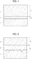
- FIG. 1 is a cross-sectional view schematically showing a preferred embodiment of a grain oriented electrical steel sheet of the invention.
- FIG. 2 is a cross-sectional view schematically showing a conventional grain oriented electrical steel sheet.
- the conventional grain oriented electrical steel sheet is typically configured such that a forsterite coating 2 is disposed on a steel sheet 1 and an insulation tension coating 3 is formed on the forsterite coating.
- the thickness T 2 of the forsterite coating 2 is about 2 pm
- the thickness T 3 of the insulation tension coating 3 is about 2 ⁇ m.
- the forsterite coating 2 in the conventional case is replaced by a ceramic coating 4.
- the ceramic coating 4 is formed by a CVD method or a PVD method on a surface of the steel sheet 1 having been smoothed by chemical polishing, electrolytic polishing or another method. Since the thickness T 4 of the ceramic coating 4 in FIG. 1 is for example not more than 1.00 ⁇ m, even if the thickness T 3 of the insulation tension coating 3 is increased to 2.0 ⁇ m or more, the effective steel sheet volume (lamination factor) of the grain oriented electrical steel sheet when used as a transformer is not decreased.
- the present inventors found that, by adjusting the rotational speed of an application roll, the specific gravity of a coating chemical solution, or another factor to thereby increase the thickness of the resulting insulation tension coating, a tension applied to the associated steel sheet is increased, and thus, the resulting grain oriented electrical steel sheet can have improved magnetic properties.
- the grain oriented electrical steel sheet of the invention is a grain oriented electrical steel sheet comprising a steel sheet, a coating layer A that is a ceramic coating containing an oxide in an amount of less than 30 mass% and disposed on the steel sheet, and a coating layer B that is an insulation tension coating containing an oxide and disposed on the coating layer A, wherein, when Gaussian fitting is performed on a 31 P-NMR spectrum of the coating layer B within a range of 0 to -60 ppm, a peak area in a range of -17 to -33 ppm accounts for 30% or more of a total peak area.
- the grain oriented electrical steel sheet of the invention is excellent in the coating adhesion property after stress relief annealing (hereinafter also simply called “coating adhesion property”) as well as in the magnetic properties after stress relief annealing (hereinafter also simply called “magnetic properties").
- the grain oriented electrical steel sheet of the invention is described below in further detail. The following description also covers the producing method of a grain oriented electrical steel sheet according to the present invention.
- the type of a steel sheet is not particularly limited, and a steel sheet described below is one example.
- the ingot for use is not limited thereto.
- Such an ingot is subjected to hot rolling and then several times of cold rolling with several times of annealing performed therebetween, to thereby obtain a final cold rolled steel sheet, which is in turn subjected to decarburization annealing and finishing annealing to allow secondary recrystallized grains having the Goss orientation to develop.
- a steel sheet is obtained.
- the number of times of cold rolling is preferably up to two times for achieving the balance between the magnetic properties and the cost.
- C is removed through decarburization annealing, and Al, N, Se and S are purified through finishing annealing, so that these components are to be contained in the steel sheet having undergone finishing annealing in trace amounts that can be regarded as the amount of inevitable impurities.
- a forsterite coating be formed on a steel sheet surface and thereafter removed by pickling.
- a forsterite coating is favorable for decarburization of a steel sheet, when another decarburization method is employed, a forsterite coating need not be formed.
- the steel sheet surface is smoothed by a method such as chemical polishing or electrolytic polishing.
- the coating adhesion property further improves owing to the anchoring effect.
- a steel sheet surface condition is smoother, a magnetic domain moves more easily, and the amount of improvement in the magnetic properties when a tension stress is applied increases, accordingly.
- the coating layer A (ceramic coating) does not peel off after stress relief annealing, and thus, an excellent coating adhesion property is maintained. Therefore, it is preferable to smooth a steel sheet surface to the extent possible by chemical polishing or electrolytic polishing so as to achieve an arithmetic mean roughness Ra of not more than 0.4 ⁇ m.
- the grain oriented electrical steel sheet of the invention has the coating layer A that is a ceramic coating disposed on a surface of the steel sheet as above.
- the amount of oxide in the coating layer A is less than 30 mass%, preferably not more than 15 mass%, more preferably not more than 5 mass% and even more preferably not more than 2 mass% because when the lattice of the ceramic coating matches the body-centered cubic lattice of the steel sheet, a more excellent coating adhesion property can be achieved.
- the amount of oxide in the ceramic coating can be measured with X-ray fluorescence using a reference sheet having a known composition.
- Exemplary elements in the oxide other than oxygen (O) include those listed as elements in a non-oxide other than C and N, which is described below.
- a component (a component other than the oxide) contained in the coating layer A (ceramic coating) is at least one selected from the group consisting of a carbide, a nitride and a carbonitride, for example.
- the coating adhesion property is further improved.
- an exemplary element in the non-oxide other than C and N is at least one selected from the group consisting of Cr, Ti, Al, Si, Zr, Mo, Y, Nb, W, Fe, Mn, Ta, Ge and Hf, and of these, at least one selected from the group consisting of Cr, Ti, Al, Si, Zr, Mo, Y, Nb and W is preferred.
- a nitride or a carbonitride having a rock salt structure is preferred for the reason that this easily matches the body-centered cubic lattice of the steel sheet.
- the non-oxide is preferably a component contributing to maximum improvement in oxidation resistance of a nitride or the like in the ceramic coating.
- a non-oxide such as a nitride containing three or more elements, e.g., TiCrN or AlCrN, can also be favorably used.
- the amount of non-oxide in the ceramic coating is preferably not less than 70 mass%. It is preferable that the ceramic coating be substantially made of the non-oxide.
- a value obtained by subtracting the amount of oxide from the total mass of the ceramic coating can be regarded as the amount of non-oxide in the ceramic coating.
- the thickness of the coating layer A is preferably not more than 1.00 ⁇ m and more preferably not more than 0.30 ⁇ m for the sake of suppressing an increase in cost.
- the thickness of the ceramic coating is preferably not less than 0.01 ⁇ m because the coating adhesion property becomes more excellent.
- a flake (cross-section) cut out using FIB (Focused Ion Beam) is observed with a TEM (Transmission Electron Microscope), and the average of measurements at given ten places is obtained.
- the method of forming the coating layer A is preferably a CVD (Chemical Vapor Deposition) method or a PVD (Physical Vapor Deposition) method.
- a preferred CVD method is a thermal CVD method.
- the coating formation temperature is preferably from 900°C to 1100°C. While the coating can be formed in the atmospheric pressure, it is preferable to reduce pressure for uniform coating formation, and thus, the pressure during coating formation is more preferably 10 to 1000 Pa for manufacturing reasons.
- a preferred PVD method is an ion plating method.
- the coating formation temperature is preferably from 300°C to 600°C for manufacturing reasons.
- the pressure during coating formation is preferably reduced and more preferably 0.1 to 100 Pa.
- a bias voltage of -10 to -100 V is preferably applied with the steel sheet serving as the cathode.
- Plasma is preferably used for ionization of a raw material because this leads to a higher coating formation rate.
- PVD methods When a ceramic coating containing three or more elements, such as TiAlN or TiCrN, preferred coating formation methods are PVD methods, with the ion plating method being more preferred.
- CVD method utilizing a thermodynamic reaction for coating formation it is sometimes difficult to obtain a desired composition; since a PVD method ionizes an alloy material and allows the material to coherently precipitate, a desired composition can easily be obtained.
- the grain oriented electrical steel sheet of the invention has the coating layer B that is an insulation tension coating containing an oxide and disposed on the coating layer A (ceramic coating).
- the proportion of the peak area in a range of -17 to -33 ppm (hereinafter called “peak area proportion" for convenience) with respect to the total peak area is 30% or more.
- the grain oriented electrical steel sheet of the invention can have excellent magnetic properties in addition to an excellent coating adhesion property.
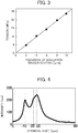
- FIG. 4 shows an example of a 31 P-NMR spectrum of the coating layer B (insulation tension coating).
- the conditions for 31 P-NMR spectrum measurement are as follows: the apparatus is VNS 600 manufactured by Agilent Technologies, Inc.; the measurement temperature is room temperature; the rotational speed is 7 kHz; and the reference sample is ammonium dihydrogenphosphate.
- the peak area proportion is preferably not less than 30%, more preferably not less than 40% and even more preferably not less than 60% because the grain oriented electrical steel sheet of the invention can have more excellent coating adhesion property and magnetic properties.
- the upper limit of the peak area proportion is not particularly limited and is, for instance, 80% or less.
- the insulation tension coating preferably includes a crystal phase.
- the crystal phase content of the insulation tension coating is preferably not less than 5 mass%, more preferably not less than 10 mass% and even more preferably not less than 15 mass%.
- the upper limit thereof is not particularly limited and is, for instance, not more than 50 mass% and preferably not more than 40 mass%.
- exemplary methods include: a quantitative method using an integrated intensity ratio of a crystalline component to an amorphous component; a quantitative method using the calibration curve of a reference sample prepared in advance; and a quantitative method using an integral intensity ratio of the crystal phase to a reference material.
- the crystal phase in the insulation tension coating is preferably a phosphate crystal phase.
- the phosphate (composition of the phosphate) is suitably determined in accordance with a component or components contained in a coating chemical solution for use, and examples thereof include, but not limited to, Mg 2 P 2 O 7 , Ca 2 P 2 O 7 , Sr 2 P 2 O 7 , Ba 2 P 2 O 7 , Al 2 P 2 O 8 , Y 2 P 2 O 8 , Cr 2 P 2 O 8 , Ti 3 P 4 O 16 , Zr 3 P 4 O 16 , Mn 3 P 4 O 16 , NbPO 5 , VPO 5 and WP 2 O 8 .
- the crystal phase is identified using, for instance, X-ray diffraction.
- the coating layer B (insulation tension coating) contains an oxide.
- the amount of oxide of phosphorus (P 2 O 5 ) in the insulation tension coating is preferably from 25 to 55 mass% and more preferably from 35 to 45 mass%.
- the amount of oxide of silicon (SiO 2 ) in the insulation tension coating is preferably from 42 to 58 mass% and more preferably from 48 to 58 mass%.
- the amount of oxide of element other than P and Si e.g., MgO, CaO, SrO, BaO, Al 2 O 3 , Y 2 O 3 , Cr 2 O 3 , TiO 2 , ZrO 2 , MnO 2 , Nb 2 O 5 , V 2 O 5 , WO 3 ) in the insulation tension coating is preferably from 2 to 18 mass% and more preferably from 2 to 12 mass%.
- the amounts of the foregoing oxides in the insulation tension coating can be measured by X-ray fluorescence spectrometry using a reference sheet with an insulation tension coating having a known composition.
- the oxides as above in the insulation tension coating are sometimes collectively called "silicon phosphate.”
- FIG. 3 is a graph showing the relationship between the thickness of an insulation tension coating and the tension that the insulation tension coating with the relevant thickness applies to the associated steel sheet. As shown in FIG. 3 , with increasing thickness of the insulation tension coating, a tension (tension stress) applied to the steel sheet increases, and as a result, the grain oriented electrical steel sheet can have excellent magnetic properties (lower iron loss).
- the thickness of the insulation tension coating is preferably not less than 1.0 ⁇ m because the grain oriented electrical steel sheet can have more excellent magnetic properties.
- the insulation tension coating When the insulation tension coating is too thick, however, this causes a decrease in effective steel sheet volume of the grain oriented electrical steel sheet when used as a transformer, and also an iron loss reducing effect exerted by the tension stress is saturated, so that transformer properties may rather deteriorate.
- the insulation tension coating preferably has a thickness of preferably not more than 10.0 ⁇ m and more preferably not more than 5.0 ⁇ m.
- the cross-section is observed using an SEM (Scanning Electron Microscope) to measure the thickness, and the average of the measurements at given ten places is obtained.
- SEM Sccanning Electron Microscope
- the method of forming the insulation tension coating is not particularly limited, and preferred examples thereof include a method involving applying a coating chemical solution onto the ceramic coating, followed by optionally drying, and then baking in a nitrogen atmosphere. This method is taken as an example and described below.
- the coating chemical solution preferably contains phosphoric acid and/or phosphate, and colloidal silica.
- exemplary metal types of the phosphate that may be preferably used include Mg, Ca, Sr, Ba, Al and Mn.
- a phosphate having a low thermal expansion coefficient such as a magnesium phosphate or an aluminum phosphate is preferred because this leads to easier formation of the crystal phase.
- a primary phosphate (biphosphate) is advantageously used from the viewpoint of availability.
- the coating chemical solution may further contain an M compound in addition to phosphoric acid and/or phosphate and colloidal silica.
- M include Y, Cr, Ti, Zr, Nb, V and W.
- Examples of the Y compound include Y 2 O 3 .
- An exemplary Cr compound is a chromic acid compound, specific examples thereof including chromic anhydride (CrO 3 ), a chromate, and a bichromate.
- Examples of the Ti compound include TiO 2 and Ti 2 O 3 .
- Zr compound examples include Zr(SO 4 ) 2 ⁇ 4H 2 O and ZrO 2 .
- Examples of the Nb compound include Nb 2 O 5 .
- V compound examples include NH 4 VO 3 and V 2 O 5 .
- Examples of the W compound include K 2 WO 4 and WO 3 .
- a phosphate may be regarded as the M compound.
- exemplary Mg compounds include Mg 3 (PO 4 ) 2
- exemplary Ca compounds include Ca 3 (PO 4 ) 2
- exemplary Al compounds include AlPO 4 .
- the amounts of respective components in the coating chemical solution are, for example, suitably adjusted to allow the resulting insulation tension coating to have the composition as described above.
- the method of applying the coating chemical solution as above onto the coating layer A is not particularly limited and preferably utilizes an application roll for manufacturing cost reasons.
- the baking temperature and the baking time are preferably 700°C to 900°C and 10 to 30 seconds, respectively, for the following reasons.
- the coating chemical solution is dried in the first stage of formation of the insulation tension coating.
- a baking temperature of not lower than 700°C and/or a baking time of not less than 10 seconds drying of the coating chemical solution sufficiently proceeds, so that moisture included in the coating chemical solution can adequately be removed, thus further improving a tension stress applied by the insulation tension coating to the steel sheet.
- oxidization of the ceramic coating caused by moisture can be suppressed during stress relief annealing.
- the baking atmosphere is preferably a nitrogen atmosphere.
- the ceramic coating When the baking atmosphere is an air atmosphere, the ceramic coating may be easily oxidized due to the presence of moisture, oxygen and the like contained in the air; however, in a nitrogen atmosphere, oxidization of the ceramic coating is suppressed, resulting in a further excellent coating adhesion property.
- coating layer B insulation tension coating
- the method of having a peak area proportion of not less than 30% there are two possible methods.
- the first method is increasing the amount of phosphoric acid and/or phosphate in the coating chemical solution (method 1).
- the amount of phosphoric acid and/or phosphate in the coating chemical solution is preferably not less than 20 mol% and more preferably not less than 30 mol% with respect to the total solids of the coating chemical solution.
- the amount of phosphoric acid and/or phosphate in the coating chemical solution is preferably not more than 50 mol% with respect to the total solids of the coating chemical solution.
- the second method is crystallizing the insulation tension coating (method 2). Specifically, in the insulation tension coating, glass in which the bond of P-O-Si is dominant is separated into a crystal portion having the chain structure of Q 2 and a glass portion having the chain structure of -Si-O-Si-O-Si-. As a result, the oxidizing ability of the insulation tension coating can be decreased, leading to an excellent coating adhesion property.
- Glass does not have a long period structure and naturally has a lower filling density than a crystal. Accordingly, when glass is crystallized, the Young's modulus of the insulation tension coating improves. Thus, the tension of the insulation tension coating improves, resulting in improved magnetic properties.
- the method 1 and the method 2 are preferably used in combination as the method of having a peak area proportion of not less than 30%.
- Exemplary methods of crystallizing the insulation tension coating include: a method involving increasing the baking temperature and the baking time (method A); and a method involving using laser light or photoinduction (method B).
- the baking temperature is preferably 870°C or higher.
- the insulation tension coating is locally applied with heat and/or strain by means of laser light or photoinduction and thereby crystalllized.
- laser light that may be preferably used is YAG laser light.
- the method B is preferred because crystal nuclei can be formed at regular intervals such that the insulation tension coating is uniformly crystallized, thus achieving further excellent coating adhesion property and magnetic properties.
- the crystallinity has the upper limit that is determined depending on the composition.
- the baking temperature and/or the baking time is increased more than needed to crystallize the insulation tension coating to the upper limit of the crystallinity, the reaction between the insulation tension coating and the ceramic coating may be accelerated and rather cause deterioration of the properties.
- the grain oriented electrical steel sheet of the invention may sometimes be subjected to stress relief annealing by a demander or the like.
- the conditions for stress relief annealing are not particularly limited, and for instance, annealing is carried out in a nitrogen or another atmosphere at a temperature of 700°C to 900°C for 2 to 4 hours.
- the technique of refining magnetic domains of the grain oriented electrical steel sheet by forming a groove near a steel sheet surface such that the groove extends across the rolling direction of the grain oriented electrical steel sheet or by introducing a strain by laser irradiation or electron beam irradiation.
- the grain oriented electrical steel sheet of the invention is, however, excellent in the coating adhesion property and the magnetic properties even when no stress relief annealing is carried out (for instance, in the case where the grain oriented electrical steel sheet is dedicated to pile iron cores). Therefore, in the present invention, when no stress relief annealing is carried out, the magnetic properties can be further improved by using the magnetic domain refining technique that introduces a strain.
- a coating layer A (ceramic coating) and a coating layer B (insulation tension coating) were formed in this order on a steel sheet as described below, thereby obtaining a grain oriented electrical steel sheet.
- the ingot was subjected to hot rolling, hot band annealing, and two times of cold rolling with intermediate annealing performed therebetween, to thereby obtain a final cold rolled steel sheet with a thickness of 0.23 mm, which was in turn subjected to decarburization annealing and finishing annealing to allow Goss orientation secondary recrystallized grains to develop.
- a steel sheet having a forsterite coating was obtained.
- the forsterite coating on a steel sheet surface was removed by pickling, whereafter the surface was smoothed by chemical polishing using hydrofluoric acid.
- the thickness of the steel sheet after the chemical polishing was 0.22 mm.
- a TiN ceramic coating with a thickness of 0.20 ⁇ m was formed on the steel sheet by a CVD method.
- the amount of oxide in the ceramic coating was not more than 2 mass% in each case.
- the thermal CVD method was used, and the coating formation was carried out under conditions of 1050°C and 1000 Pa.
- the coating chemical solution was prepared by selecting one or more from among phosphate, colloidal silica (AT-30 manufactured by ADEKA Corporation; average particle size, 10 nm) and an M compound and blending the selected component(s) such that the resulting insulation tension coating can have one of the compositions A to C shown in Table 1 below.
- the amount of phosphoric acid and/or phosphate in each coating chemical solution was within a range of 20 to 30 mol% with respect to the total solids of the coating chemical solution.
- compositions A to C shown in Table 1 below are as follows.
- composition A represents that the amount of P 2 O 5 is "40 mass%,” the amount of SiO 2 is “55 mass%,” and the amount of MgO is “5 mass%” (the same applies to the others).
- the crystal phase (phosphate crystal phase) of the insulation tension coating was identified using X-ray diffraction. The results are shown in Table 1 below. For the cases where the identification was not carried out, "-" was given in Table 1 below.
- the quantity of the crystal phase of each inventive example was determined and as a result was within a range of 5 to 10 mass% in each case.
- a quantitative method using X-ray diffraction and determining the quantity based on an integral intensity ratio of a crystalline component to a non-crystalline component was employed.
- a 31 P-NMR spectrum of the insulation tension coating was measured.
- the measurement conditions were as follows: the apparatus was VNS 600 manufactured by Agilent Technologies, Inc.; the measurement temperature was room temperature; the rotational speed was 7 kHz; and the reference sample was ammonium dihydrogenphosphate.
- the apparatus was VNS 600 manufactured by Agilent Technologies, Inc.
- the measurement temperature was room temperature
- the rotational speed was 7 kHz
- the reference sample was ammonium dihydrogenphosphate.
- FIG. 4 One example of measured 31 P-NMR spectra is shown in FIG. 4 .
- the grain oriented electrical steel sheet having undergone stress relief annealing was wound around round bars having diameters different on a 5-millimeter basis, i.e., diameters of 5 mm, 10 mm, ... (but including a round bar having a diameter of 3 mm) to determine the minimum diameter (unit: mm) from among diameters with which the ceramic coating did not peel off.
- the results are shown in Table 1 below. As the minimum diameter of diameters with which the coating does not peel off (i.e., no peel-off diameter) is smaller, the coating adhesion property after stress relief annealing can be rated as more excellent, and a no peel-off diameter of less than 30 mm is favorable.
- the iron loss W 17/50 was measured. The results are shown in Table 1 below. For the cases where the iron loss W 17/50 was not measured, "-" was given in Table 1 below. When the iron loss W 17/50 (unit: W/kg) is less than 0.80, the magnetic properties after stress relief annealing can be rated as excellent.
- the no peel-off diameter is up to 20 mm and thus small, which means an excellent coating adhesion property
- the iron loss W 17/50 is less than 0.80, which means excellent magnetic properties.
- a coating layer A (ceramic coating) and a coating layer B (insulation tension coating) were formed in this order on a steel sheet as described below, thereby obtaining a grain oriented electrical steel sheet.
- the ingot was subjected to hot rolling, hot band annealing, and two times of cold rolling with intermediate annealing performed therebetween, to thereby obtain a final cold rolled steel sheet with a thickness of 0.23 mm, which was in turn subjected to decarburization annealing and finishing annealing to allow Goss orientation secondary recrystallized grains to develop.
- a steel sheet having a forsterite coating was obtained.
- the forsterite coating on a steel sheet surface was removed by pickling, whereafter the surface was smoothed by chemical polishing using hydrofluoric acid.
- the thickness of the steel sheet after the chemical polishing was 0.22 mm.
- a TiN ceramic coating with a thickness of 0.20 ⁇ m was formed on the steel sheet by a CVD method.
- the amount of oxide in the ceramic coating was not more than 2 mass% in each case.
- the thermal CVD method was used, and the coating formation was carried out under conditions of 1050°C and 1000 Pa.
- the insulation tension coating was irradiated with laser light and thereby crystallized.
- laser light YAG laser light was used.
- the coating chemical solution was prepared by selecting one or more from among phosphate, colloidal silica (AT-30 manufactured by ADEKA Corporation; average particle size, 10 nm) and an M compound and blending the selected component(s) such that the resulting insulation tension coating can have the composition as stated in Table 2 below.
- the amount of phosphoric acid and/or phosphate in each coating chemical solution was within a range of 20 to 30 mol% with respect to the total solids of the coating chemical solution.
- the crystal phase (phosphate crystal phase) of the insulation tension coating was identified and quantified in the same manners as in Test Example 1. The identification results are shown in Table 2 below. The quantity of the crystal phase was determined and as a result was within a range of 5 to 10 mass% in each case.
- the no peel-off diameter is up to 20 mm and thus small, which means an excellent coating adhesion property
- the iron loss W 17/50 is less than 0.80, which means excellent magnetic properties.
- a coating layer A (ceramic coating) and a coating layer B (insulation tension coating) were formed in this order on a steel sheet as described below, thereby obtaining a grain oriented electrical steel sheet.
- the ingot was subjected to hot rolling, hot band annealing, and two times of cold rolling with intermediate annealing performed therebetween, to thereby obtain a final cold rolled steel sheet with a thickness of 0.23 mm, which was in turn subjected to decarburization annealing and finishing annealing to allow Goss orientation secondary recrystallized grains to develop.
- a steel sheet having a forsterite coating was obtained.
- the forsterite coating on a steel sheet surface was removed by pickling, whereafter the surface was smoothed by chemical polishing using hydrofluoric acid.
- the thickness of the steel sheet after the chemical polishing was 0.22 mm.
- a ceramic coating having the composition shown in Table 3 below was formed to have a thickness shown in Table 3 below on the steel sheet by a CVD method or a PVD method.
- the amount of oxide in the ceramic coating was not more than 2 mass% in each case.
- the thermal CVD method was used, and the coating formation was carried out under conditions of 1050°C and 1000 Pa.
- the PVD method the ion plating method was used, and the coating formation was carried out under conditions of 450°C, 3 Pa and a bias voltage of -20 V.
- the insulation tension coating was irradiated with laser light and thereby crystallized.
- laser light YAG laser light was used.
- the same coating chemical solution as that of No. 1 in Test Example 2 was used.
- the crystal phase and the peak area proportion of the formed insulation tension coating (composition: 40P 2 O 5 -55SiO 2 -5MgO) were also the same as those of No. 1 in Test Example 2.
- the no peel-off diameter is less than 30 mm, which means an excellent coating adhesion property
- the iron loss W 17/50 is less than 0.80, which means excellent magnetic properties.
- a coating layer A (ceramic coating) and a coating layer B (insulation tension coating) were formed in this order on a steel sheet as described below, thereby obtaining a grain oriented electrical steel sheet.
- the ingot was subjected to hot rolling, hot band annealing, and two times of cold rolling with intermediate annealing performed therebetween, to thereby obtain a final cold rolled steel sheet with a thickness of 0.23 mm, which was in turn subjected to decarburization annealing and finishing annealing to allow Goss orientation secondary recrystallized grains to develop.
- a steel sheet having a forsterite coating was obtained.
- the forsterite coating on a steel sheet surface was removed by pickling, whereafter the surface was smoothed by chemical polishing using hydrofluoric acid.
- the thickness of the steel sheet after the chemical polishing was 0.20 mm.
- an AlCrN ceramic coating with a thickness of 0.10 ⁇ m was formed on the steel sheet by a PVD method.
- the amount of oxide in the ceramic coating was not more than 2 mass% in each case.
- the ion plating method was used, and the coating formation was carried out under conditions of 450°C, 3 Pa and a bias voltage of -20 V.
- the insulation tension coating was irradiated with laser light and thereby crystallized.
- laser light YAG laser light was used.
- the same coating chemical solution as that of No. 1 in Test Example 2 was used.
- the crystal phase and the peak area proportion of the formed insulation tension coating (composition: 40P 2 O 5 -55SiO 2 -5MgO) were also the same as those of No. 1 in Test Example 2.
- the no peel-off diameter is less than 30 mm, which means an excellent coating adhesion property
- the iron loss W 17/50 is less than 0.80, which means excellent magnetic properties.
Landscapes
- Chemical & Material Sciences (AREA)
- Engineering & Computer Science (AREA)
- Materials Engineering (AREA)
- Mechanical Engineering (AREA)
- Metallurgy (AREA)
- Organic Chemistry (AREA)
- Chemical Kinetics & Catalysis (AREA)
- General Chemical & Material Sciences (AREA)
- Physics & Mathematics (AREA)
- Inorganic Chemistry (AREA)
- Electromagnetism (AREA)
- Crystallography & Structural Chemistry (AREA)
- Thermal Sciences (AREA)
- Power Engineering (AREA)
- Dispersion Chemistry (AREA)
- Manufacturing & Machinery (AREA)
- Chemical Treatment Of Metals (AREA)
- Soft Magnetic Materials (AREA)
- Manufacturing Of Steel Electrode Plates (AREA)
- Other Surface Treatments For Metallic Materials (AREA)
- Physical Vapour Deposition (AREA)
- Chemical Vapour Deposition (AREA)
Abstract
Description
- The present invention relates to a grain oriented electrical steel sheet and a producing method of a grain oriented electrical steel sheet.
- Grain oriented electrical steel sheets are soft magnetic materials used as materials for iron cores of transformers, generators and the like. Grain oriented electrical steel sheets are characterized in having a crystal structure in which the <001> orientation that is an easy magnetization axis of iron is highly-precisely aligned in the rolling direction of the steel sheet. The texture as above is formed through finishing annealing of a manufacturing process of a grain oriented electrical steel sheet, which finishing annealing allows crystal grains with the {110}<001> orientation referred to as the so-called Goss orientation to preferentially grow to an enormous size. Grain oriented electrical steel sheets as products are required to have such magnetic properties as high magnetic flux density and low iron loss.
- The magnetic properties of a grain oriented electrical steel sheet are improved by applying a tensile stress (tension) to a steel sheet surface. As one conventional technique of applying a tensile stress to a steel sheet, a technique in which a forsterite coating of about 2 µm thickness is formed on a steel sheet surface and another coating of about 2 µm thickness primarily composed of silicon phosphate is formed on the forsterite coating is typically used.
- To be more specific, the silicon phosphate coating having a lower thermal expansion coefficient than that of the steel sheet is formed at high temperature and cooled to room temperature, whereby a tensile stress is applied to the steel sheet using a difference in thermal expansion coefficient between the steel sheet and the silicon phosphate coating.
- This silicon phosphate coating also acts as an insulating coating that is indispensable for a grain oriented electrical steel sheet. Owing to the insulation, a local eddy current is prevented from being generated in the steel sheet.
- A surface of the grain oriented electrical steel sheet having undergone finishing annealing is smoothed by chemical polishing or electrolytic polishing, and then a tensile stress is applied by means of the coating above the steel sheet, whereby iron loss can remarkably be decreased.
- Meanwhile, the forsterite coating between the steel sheet and the silicon phosphate coating adheres to the steel sheet owing to the anchoring effect. Therefore, the smoothness of the steel sheet surface inevitably deteriorates. The adhesion between silicon phosphate and metal is so low that a silicon phosphate coating cannot be formed directly on a mirror-finished surface of a steel sheet. Thus, in the coating structure of a conventional grain oriented electrical steel sheet (steel sheet/ forsterite coating/ silicon phosphate coating), a surface of a steel sheet cannot be smoothed.
- In
Patent Literature 1, in order to maintain the smoothness of a steel sheet surface and also apply a large tensile stress to the steel sheet, a ceramic coating made of TiN for instance is formed on the steel sheet by a CVD method or a PVD method. At this time, since a tensile stress applied to the steel sheet is proportional to the thickness of the ceramic coating, the ceramic coating is formed to have a thickness of at least 1 µm. - CVD methods and PVD methods, however, cause high manufacturing costs, and accordingly, coatings are desired to have a small thickness to the utmost extent, which in turn results in a decrease in tensile stress applied to a steel sheet.
- In
Patent Literature 2, to compensate a decrease in tension due to such a small coating thickness or to apply a much higher tension to a steel sheet, an insulation tension coating made of silicon phosphate is formed on a ceramic coating with a thickness of 1 µm or less. -
- Patent Literature 1:
JP 01-176034 A - Patent Literature 2:
JP 64-068425 A - The present inventors studied a grain oriented electrical steel sheet in which an insulation tension coating was formed on a ceramic coating. As a result, it was found that when a demander or the like subjects the grain oriented electrical steel sheet to stress relief annealing, this sometimes causes the ceramic coating to peel off from the associated steel sheet or results in poor magnetic properties of the grain oriented electrical steel sheet.
- The present invention has been made in view of the above and aims at providing a grain oriented electrical steel sheet having excellent coating adhesion property and magnetic properties after stress relief annealing, as well as a producing method thereof.
- The present inventors have made an intensive study to achieve the foregoing objects and as a result found that, when specific coating structures are employed for a ceramic coating and an insulation tension coating, the coating adhesion property and the magnetic properties are both excellent even after stress relief annealing. The invention has been thus completed.
- Specifically, the present invention provides the following [1] to [13].
- [1] A grain oriented electrical steel sheet, comprising:
- a steel sheet;
- a coating layer A that is a ceramic coating containing an oxide in an amount of less than 30 mass% and disposed on the steel sheet; and
- a coating layer B that is an insulation tension coating containing an oxide and disposed on the coating layer A,
- wherein when Gaussian fitting is performed on a 31P-NMR spectrum of the coating layer B within a range of 0 to -60 ppm, a peak area in a range of -17 to -33 ppm accounts for 30% or more of a total peak area.
- [2] The grain oriented electrical steel sheet according to [1] above,
wherein the coating layer B includes not less than 5 mass% of crystal phase. - [3] The grain oriented electrical steel sheet according to [2] above,
wherein the crystal phase is a phosphate crystal phase. - [4] The grain oriented electrical steel sheet according to any one of [1] to [3] above,
wherein the coating layer A has a thickness of not less than 0.01 µm. - [5] The grain oriented electrical steel sheet according to any one of [1] to [4] above,
wherein the coating layer A has a thickness of not more than 0.30 µm. - [6] The grain oriented electrical steel sheet according to any one of [1] to [5] above,
wherein the coating layer B has a thickness of not less than 1.0 µm. - [7] The grain oriented electrical steel sheet according to any one of [1] to [6] above,
wherein the coating layer B has a thickness of not more than 10.0 µm. - [8] The grain oriented electrical steel sheet according to any one of [1] to [7] above,
wherein the coating layer A contains a nitride or a carbonitride. - [9] A grain oriented electrical steel sheet producing method of producing the grain oriented electrical steel sheet according to any one of [1] to [8] above,
wherein the coating layer B is formed by applying a coating chemical solution onto the coating layer A and baking the coating chemical solution in a nitrogen atmosphere. - [10] The grain oriented electrical steel sheet producing method according to [9] above,
wherein an amount of phosphoric acid and/or phosphate in the coating chemical solution is not less than 20 mol% with respect to total solids of the coating chemical solution. - [11] The grain oriented electrical steel sheet producing method according to [9] or [10] above,
wherein the baking is followed by crystallization using laser light or photoinduction, thereby obtaining the coating layer B. - [12] The grain oriented electrical steel sheet producing method according to any one of [9] to [11] above,
wherein the coating chemical solution is applied with an application roll. - [13] The grain oriented electrical steel sheet producing method according to any one of [9] to [12],
wherein the coating layer A is formed by a chemical vapor deposition method or a physical vapor deposition method. - The present invention can provide a grain oriented electrical steel sheet having excellent coating adhesion property and magnetic properties after stress relief annealing, as well as a producing method thereof.
-
-
FIG. 1 is a cross-sectional view schematically showing a preferred embodiment of a grain oriented electrical steel sheet of the invention. -
FIG. 2 is a cross-sectional view schematically showing a conventional grain oriented electrical steel sheet. -
FIG. 3 is a graph showing the relationship between the thickness of an insulation tension coating and the tension that the insulation tension coating with the relevant thickness applies to the associated steel sheet. -
FIG. 4 shows an example of a 31P-NMR spectrum of an insulation tension coating. - A ceramic coating with a thickness of not more than 1.00 µm (e.g., 0.30 µm) was formed on a steel sheet, and an insulation tension coating made of silicon phosphate was formed thereon; when the resulting steel sheet was subjected to stress relief annealing, the ceramic coating peeled off from the steel sheet (i.e., the coating adhesion property deteriorated) in some cases. The present inventors conducted many experiments to find out why this occurred and now have the following ideas.
- The use of silicon phosphate having a low thermal expansion coefficient as a material for the insulation tension coating is advantageous for increasing a tensile stress applied by the insulation tension coating to the associated steel sheet and thereby improving the magnetic properties, while components in the insulation tension coating oxidize the ceramic coating under a high temperature environment, thus generating reaction products.
- Subsequently, the reaction products diffuse in the ceramic coating from the interface between the insulation tension coating and the ceramic coating toward the steel sheet during stress relief annealing at 800°C for 3 hours; when the reaction products further diffuse and reach the interface between the ceramic coating and the steel sheet, they react with Fe of the steel sheet and form precipitates.
- Then, during a cooling process in stress relief annealing, i.e., when a stress starts to be applied to the interface between the steel sheet and the ceramic coating due to a difference in thermal expansion coefficient, the precipitates cannot fully receive the stress and consequently peel off from the steel sheet. Thus, the ceramic coating peels off from the steel sheet. In other words, the coating adhesion property deteriorates.
- To cope with it, the present inventors considered suppressing the oxidation reaction of the ceramic coating (e.g., nitride-containing ceramic coating) caused by the insulation tension coating containing an oxide.
- The oxidizing ability of oxides can be explained using the electronegativity. To be more specific, when such bonds as P-O-P, P-O-Si and P-O-M (M: metal) are taken as an example, a P-O-P bond including a larger amount of P which is the most electronegative element should be most unlikely to cause an oxidation reaction. Accordingly, when a phosphorus oxide in the insulation tension coating has the chain structure of -P-O-P-O-P- and the like, the oxidizing ability of the phosphorus oxide decreases.
- The structure of glass is typically evaluated using 31P-NMR (Nuclear Magnetic Resonance). In a 31P-NMR spectrum, when a peak appears in a chemical shift range of not more than -17 ppm, the peak can be determined to indicate one of the chain structures of phosphorus oxides called Q2 and Q3 expressed by the formulae shown below (T. Kasuga, Journal of the Society of Inorganic Materials Japan 10 (2003) 189.).

- The present inventors formed, after finishing annealing, a ceramic coating made of a nitride and other components and having a thickness of not larger than 0.30 µm on a steel sheet from whose surface a forsterite coating had been removed by pickling. Thereafter, a coating chemical solution was applied on the ceramic coating with an application roll and baked in a nitrogen atmosphere, thereby forming an insulation tension coating. Then, stress relief annealing was carried out at 800°C for 3 hours in a nitrogen atmosphere.
- At this time, the present inventors performed Gaussian fitting on a 31P-NMR spectrum of the insulation tension coating within a range of 0 to -60 ppm and as a result found that, when the peak area in a range of -17 to -33 ppm accounts for 30% or more of the total peak area, even if the thickness of the ceramic coating is 1.00 µm or less, an excellent coating adhesion property can be maintained after stress relief annealing.
-
FIG. 1 is a cross-sectional view schematically showing a preferred embodiment of a grain oriented electrical steel sheet of the invention.FIG. 2 is a cross-sectional view schematically showing a conventional grain oriented electrical steel sheet. - First, as shown in
FIG. 2 , the conventional grain oriented electrical steel sheet is typically configured such that aforsterite coating 2 is disposed on asteel sheet 1 and aninsulation tension coating 3 is formed on the forsterite coating. InFIG. 2 , the thickness T2 of theforsterite coating 2 is about 2 pm, and the thickness T3 of theinsulation tension coating 3 is about 2 µm. - On the other hand, in
FIG. 1 , theforsterite coating 2 in the conventional case (seeFIG. 2 ) is replaced by aceramic coating 4. To be more specific, theceramic coating 4 is formed by a CVD method or a PVD method on a surface of thesteel sheet 1 having been smoothed by chemical polishing, electrolytic polishing or another method. Since the thickness T4 of theceramic coating 4 inFIG. 1 is for example not more than 1.00 µm, even if the thickness T3 of theinsulation tension coating 3 is increased to 2.0 µm or more, the effective steel sheet volume (lamination factor) of the grain oriented electrical steel sheet when used as a transformer is not decreased. - Since a tension applied by a coating to a steel sheet is usually proportional to the thickness of the coating, increasing the thickness of the insulation tension coating should be effective at improving the magnetic properties.
- The present inventors found that, by adjusting the rotational speed of an application roll, the specific gravity of a coating chemical solution, or another factor to thereby increase the thickness of the resulting insulation tension coating, a tension applied to the associated steel sheet is increased, and thus, the resulting grain oriented electrical steel sheet can have improved magnetic properties.
- Again, the grain oriented electrical steel sheet of the invention is described below.
- The grain oriented electrical steel sheet of the invention is a grain oriented electrical steel sheet comprising a steel sheet, a coating layer A that is a ceramic coating containing an oxide in an amount of less than 30 mass% and disposed on the steel sheet, and a coating layer B that is an insulation tension coating containing an oxide and disposed on the coating layer A, wherein, when Gaussian fitting is performed on a 31P-NMR spectrum of the coating layer B within a range of 0 to -60 ppm, a peak area in a range of -17 to -33 ppm accounts for 30% or more of a total peak area.
- The grain oriented electrical steel sheet of the invention is excellent in the coating adhesion property after stress relief annealing (hereinafter also simply called "coating adhesion property") as well as in the magnetic properties after stress relief annealing (hereinafter also simply called "magnetic properties").
- The grain oriented electrical steel sheet of the invention is described below in further detail. The following description also covers the producing method of a grain oriented electrical steel sheet according to the present invention.
- The type of a steel sheet is not particularly limited, and a steel sheet described below is one example.
- As the ingot that forms a steel sheet, an ingot containing, as components in steel, in percentage by mass, C in an amount from 0.002% to 0.10%, Si in an amount from 2.5% to 4.0% and Mn in an amount from 0.005% to 0.50% and also containing Al in an amount from 0.010% to 0.050% and N in an amount from 0.003% to 0.020% or Al in an amount from 0.010% to 0.050%, N in an amount from 0.003% to 0.020%, Se in an amount from 0.003% to 0.030% and/or S in an amount from 0.002% to 0.03%, with the balance being inevitable impurities and Fe is preferably used for the sake of the magnetic properties. However, the ingot for use is not limited thereto.
- Such an ingot is subjected to hot rolling and then several times of cold rolling with several times of annealing performed therebetween, to thereby obtain a final cold rolled steel sheet, which is in turn subjected to decarburization annealing and finishing annealing to allow secondary recrystallized grains having the Goss orientation to develop. Thus, a steel sheet is obtained. In this process, the number of times of cold rolling is preferably up to two times for achieving the balance between the magnetic properties and the cost.
- Of the foregoing components in steel, C is removed through decarburization annealing, and Al, N, Se and S are purified through finishing annealing, so that these components are to be contained in the steel sheet having undergone finishing annealing in trace amounts that can be regarded as the amount of inevitable impurities.
- Thereafter, a forsterite coating on a steel sheet surface is removed by pickling or another method.
- Thus, it is preferred from the manufacturing aspect that, as conventionally carried out, a forsterite coating be formed on a steel sheet surface and thereafter removed by pickling. Although the formation of a forsterite coating is favorable for decarburization of a steel sheet, when another decarburization method is employed, a forsterite coating need not be formed.
- After the forsterite coating is removed from the steel sheet surface, the steel sheet surface is smoothed by a method such as chemical polishing or electrolytic polishing.
- Usually, as a steel sheet surface condition is rougher, the coating adhesion property further improves owing to the anchoring effect. In contrast, as a steel sheet surface condition is smoother, a magnetic domain moves more easily, and the amount of improvement in the magnetic properties when a tension stress is applied increases, accordingly.
- In the present invention, even when use is made of a steel sheet having undergone chemical polishing that can smooth a steel sheet surface the most, the coating layer A (ceramic coating) does not peel off after stress relief annealing, and thus, an excellent coating adhesion property is maintained. Therefore, it is preferable to smooth a steel sheet surface to the extent possible by chemical polishing or electrolytic polishing so as to achieve an arithmetic mean roughness Ra of not more than 0.4 µm.
- The grain oriented electrical steel sheet of the invention has the coating layer A that is a ceramic coating disposed on a surface of the steel sheet as above.
- The amount of oxide in the coating layer A (ceramic coating) is less than 30 mass%, preferably not more than 15 mass%, more preferably not more than 5 mass% and even more preferably not more than 2 mass% because when the lattice of the ceramic coating matches the body-centered cubic lattice of the steel sheet, a more excellent coating adhesion property can be achieved.
- The amount of oxide in the ceramic coating can be measured with X-ray fluorescence using a reference sheet having a known composition.
- Exemplary elements in the oxide other than oxygen (O) include those listed as elements in a non-oxide other than C and N, which is described below.
- A component (a component other than the oxide) contained in the coating layer A (ceramic coating) is at least one selected from the group consisting of a carbide, a nitride and a carbonitride, for example.
- When the ceramic coating contains a nitride or a carbonitride, the coating adhesion property is further improved.
- When the non-oxide is at least one selected from the group consisting of a carbide, a nitride and a carbonitride, an exemplary element in the non-oxide other than C and N is at least one selected from the group consisting of Cr, Ti, Al, Si, Zr, Mo, Y, Nb, W, Fe, Mn, Ta, Ge and Hf, and of these, at least one selected from the group consisting of Cr, Ti, Al, Si, Zr, Mo, Y, Nb and W is preferred.
- For the non-oxide, a nitride or a carbonitride having a rock salt structure is preferred for the reason that this easily matches the body-centered cubic lattice of the steel sheet.
- The non-oxide is preferably a component contributing to maximum improvement in oxidation resistance of a nitride or the like in the ceramic coating. According to the Arrhenius plot formulated by P. Panjan et al. (P. Panjan et al., Thin Solid Films 281-282 (1996) 298.), the addition of Ti or the like to a Cr-containing nitride can bring about increased oxidation resistance. Accordingly, a non-oxide such as a nitride containing three or more elements, e.g., TiCrN or AlCrN, can also be favorably used.
- The amount of non-oxide in the ceramic coating is preferably not less than 70 mass%. It is preferable that the ceramic coating be substantially made of the non-oxide.
- In the present invention, a value obtained by subtracting the amount of oxide from the total mass of the ceramic coating can be regarded as the amount of non-oxide in the ceramic coating.
- The thickness of the coating layer A (ceramic coating) is preferably not more than 1.00 µm and more preferably not more than 0.30 µm for the sake of suppressing an increase in cost.
- On the other hand, the thickness of the ceramic coating is preferably not less than 0.01 µm because the coating adhesion property becomes more excellent.
- For the thickness of the ceramic coating, a flake (cross-section) cut out using FIB (Focused Ion Beam) is observed with a TEM (Transmission Electron Microscope), and the average of measurements at given ten places is obtained.
- The method of forming the coating layer A (ceramic coating) is preferably a CVD (Chemical Vapor Deposition) method or a PVD (Physical Vapor Deposition) method.
- A preferred CVD method is a thermal CVD method. The coating formation temperature is preferably from 900°C to 1100°C. While the coating can be formed in the atmospheric pressure, it is preferable to reduce pressure for uniform coating formation, and thus, the pressure during coating formation is more preferably 10 to 1000 Pa for manufacturing reasons.
- A preferred PVD method is an ion plating method. The coating formation temperature is preferably from 300°C to 600°C for manufacturing reasons. The pressure during coating formation is preferably reduced and more preferably 0.1 to 100 Pa. During the coating formation, a bias voltage of -10 to -100 V is preferably applied with the steel sheet serving as the cathode. Plasma is preferably used for ionization of a raw material because this leads to a higher coating formation rate.
- When a ceramic coating containing three or more elements, such as TiAlN or TiCrN, is formed, preferred coating formation methods are PVD methods, with the ion plating method being more preferred. When a CVD method utilizing a thermodynamic reaction for coating formation is used, it is sometimes difficult to obtain a desired composition; since a PVD method ionizes an alloy material and allows the material to coherently precipitate, a desired composition can easily be obtained.
- The grain oriented electrical steel sheet of the invention has the coating layer B that is an insulation tension coating containing an oxide and disposed on the coating layer A (ceramic coating).
- When Gaussian fitting is performed on a 31P-NMR spectrum of the coating layer B (insulation tension coating) within a range of 0 to -60 ppm, the proportion of the peak area in a range of -17 to -33 ppm (hereinafter called "peak area proportion" for convenience) with respect to the total peak area is 30% or more.
- With this configuration, the grain oriented electrical steel sheet of the invention can have excellent magnetic properties in addition to an excellent coating adhesion property.
- Taking the 31P-NMR spectrum shown in
FIG. 4 as an example, the method of determining the peak area proportion above is described in further detail.FIG. 4 shows an example of a 31P-NMR spectrum of the coating layer B (insulation tension coating). The conditions for 31P-NMR spectrum measurement are as follows: the apparatus is VNS 600 manufactured by Agilent Technologies, Inc.; the measurement temperature is room temperature; the rotational speed is 7 kHz; and the reference sample is ammonium dihydrogenphosphate. - In
FIG. 4 , three peaks are observed in a 31P chemical shift range of 0 to -60 ppm. That is, the three peaks are present with their peak tops being at -10 ppm, -22 ppm and -25 ppm in order from left inFIG. 4 . - Gaussian fitting is performed for each peak to separate the peaks, and the peak area of each separated peak is obtained. In
FIG. 4 , the sum of the peak areas of the three peaks above is the "total peak area." - The sum of the peak areas of peaks with their peak tops being positioned within a range of "-17 to -33 ppm" (in
FIG. 4 , the two peaks with their peak tops being at -22 ppm and -25 ppm) is the "peak area in a range of -17 to -33 ppm." - Then, the proportion of the "peak area in a range of -17 to -33 ppm" with respect to the "total peak area" (i.e., peak area proportion) is obtained.
- The peak area proportion is preferably not less than 30%, more preferably not less than 40% and even more preferably not less than 60% because the grain oriented electrical steel sheet of the invention can have more excellent coating adhesion property and magnetic properties.
- The upper limit of the peak area proportion is not particularly limited and is, for instance, 80% or less.
- As described below, in order to have a peak area proportion of not less than 30%, it is preferable to crystallize the insulation tension coating, and accordingly, the insulation tension coating preferably includes a crystal phase.
- The crystal phase content of the insulation tension coating is preferably not less than 5 mass%, more preferably not less than 10 mass% and even more preferably not less than 15 mass%. The upper limit thereof is not particularly limited and is, for instance, not more than 50 mass% and preferably not more than 40 mass%.
- For the quantitative method of the crystal phase, methods using X-ray diffraction are simple and easy, and exemplary methods include: a quantitative method using an integrated intensity ratio of a crystalline component to an amorphous component; a quantitative method using the calibration curve of a reference sample prepared in advance; and a quantitative method using an integral intensity ratio of the crystal phase to a reference material.
- The crystal phase in the insulation tension coating is preferably a phosphate crystal phase.
- The phosphate (composition of the phosphate) is suitably determined in accordance with a component or components contained in a coating chemical solution for use, and examples thereof include, but not limited to, Mg2P2O7, Ca2P2O7, Sr2P2O7, Ba2P2O7, Al2P2O8, Y2P2O8, Cr2P2O8, Ti3P4O16, Zr3P4O16, Mn3P4O16, NbPO5, VPO5 and WP2O8.
- The crystal phase is identified using, for instance, X-ray diffraction.
- The coating layer B (insulation tension coating) contains an oxide.
- The amount of oxide of phosphorus (P2O5) in the insulation tension coating is preferably from 25 to 55 mass% and more preferably from 35 to 45 mass%.
- The amount of oxide of silicon (SiO2) in the insulation tension coating is preferably from 42 to 58 mass% and more preferably from 48 to 58 mass%.
- In addition, the amount of oxide of element other than P and Si (e.g., MgO, CaO, SrO, BaO, Al2O3, Y2O3, Cr2O3, TiO2, ZrO2, MnO2, Nb2O5, V2O5, WO3) in the insulation tension coating is preferably from 2 to 18 mass% and more preferably from 2 to 12 mass%.
- The amounts of the foregoing oxides in the insulation tension coating can be measured by X-ray fluorescence spectrometry using a reference sheet with an insulation tension coating having a known composition.
- In the present description, the oxides as above in the insulation tension coating are sometimes collectively called "silicon phosphate."
-
FIG. 3 is a graph showing the relationship between the thickness of an insulation tension coating and the tension that the insulation tension coating with the relevant thickness applies to the associated steel sheet. As shown inFIG. 3 , with increasing thickness of the insulation tension coating, a tension (tension stress) applied to the steel sheet increases, and as a result, the grain oriented electrical steel sheet can have excellent magnetic properties (lower iron loss). - The thickness of the insulation tension coating is preferably not less than 1.0 µm because the grain oriented electrical steel sheet can have more excellent magnetic properties.
- When the insulation tension coating is too thick, however, this causes a decrease in effective steel sheet volume of the grain oriented electrical steel sheet when used as a transformer, and also an iron loss reducing effect exerted by the tension stress is saturated, so that transformer properties may rather deteriorate. Thus, the insulation tension coating preferably has a thickness of preferably not more than 10.0 µm and more preferably not more than 5.0 µm.
- For the thickness of the insulation tension coating, the cross-section is observed using an SEM (Scanning Electron Microscope) to measure the thickness, and the average of the measurements at given ten places is obtained.
- The method of forming the insulation tension coating is not particularly limited, and preferred examples thereof include a method involving applying a coating chemical solution onto the ceramic coating, followed by optionally drying, and then baking in a nitrogen atmosphere. This method is taken as an example and described below.
- The coating chemical solution preferably contains phosphoric acid and/or phosphate, and colloidal silica. Exemplary metal types of the phosphate that may be preferably used include Mg, Ca, Sr, Ba, Al and Mn.
- For the phosphate, a phosphate having a low thermal expansion coefficient such as a magnesium phosphate or an aluminum phosphate is preferred because this leads to easier formation of the crystal phase.
- As the phosphate, a primary phosphate (biphosphate) is advantageously used from the viewpoint of availability.
- The coating chemical solution may further contain an M compound in addition to phosphoric acid and/or phosphate and colloidal silica. Specific examples of M include Y, Cr, Ti, Zr, Nb, V and W.
- Examples of the Y compound include Y2O3.
- An exemplary Cr compound is a chromic acid compound, specific examples thereof including chromic anhydride (CrO3), a chromate, and a bichromate.
- Examples of the Ti compound include TiO2 and Ti2O3.
- Examples of the Zr compound include Zr(SO4)2 · 4H2O and ZrO2.
- Examples of the Nb compound include Nb2O5.
- Examples of the V compound include NH4VO3 and V2O5.
- Examples of the W compound include K2WO4 and WO3.
- A phosphate may be regarded as the M compound. For instance, exemplary Mg compounds include Mg3(PO4)2, exemplary Ca compounds include Ca3(PO4)2, and exemplary Al compounds include AlPO4.
- The amounts of respective components in the coating chemical solution are, for example, suitably adjusted to allow the resulting insulation tension coating to have the composition as described above.
- The method of applying the coating chemical solution as above onto the coating layer A (ceramic coating) is not particularly limited and preferably utilizes an application roll for manufacturing cost reasons.
- The baking temperature and the baking time are preferably 700°C to 900°C and 10 to 30 seconds, respectively, for the following reasons.
- With a baking temperature of up to 900°C and/or a baking time of up to 30 seconds, a reaction upon which precipitates are formed to cause a poor coating adhesion property between the ceramic coating and the insulation tension coating can be further suppressed, resulting in a further excellent coating adhesion property.
- The coating chemical solution is dried in the first stage of formation of the insulation tension coating. With a baking temperature of not lower than 700°C and/or a baking time of not less than 10 seconds, drying of the coating chemical solution sufficiently proceeds, so that moisture included in the coating chemical solution can adequately be removed, thus further improving a tension stress applied by the insulation tension coating to the steel sheet. In addition, oxidization of the ceramic coating caused by moisture can be suppressed during stress relief annealing.
- The baking atmosphere is preferably a nitrogen atmosphere.
- When the baking atmosphere is an air atmosphere, the ceramic coating may be easily oxidized due to the presence of moisture, oxygen and the like contained in the air; however, in a nitrogen atmosphere, oxidization of the ceramic coating is suppressed, resulting in a further excellent coating adhesion property.
- For the coating layer B (insulation tension coating), as the method of having a peak area proportion of not less than 30%, there are two possible methods.
- The first method is increasing the amount of phosphoric acid and/or phosphate in the coating chemical solution (method 1).
- Specifically, the amount of phosphoric acid and/or phosphate in the coating chemical solution is preferably not less than 20 mol% and more preferably not less than 30 mol% with respect to the total solids of the coating chemical solution.
- In the
method 1, when the amount of phosphoric acid and/or phosphate is too large, the structure called Q3 becomes dominant, and the reactivity at the double bond portion of P=O increases. While the reaction at the double bond portion does not adversely affect the coating adhesion property, gas that is a reaction product may make holes in the insulation tension coating, resulting in poor tension. - Therefore, the amount of phosphoric acid and/or phosphate in the coating chemical solution is preferably not more than 50 mol% with respect to the total solids of the coating chemical solution.
- The second method is crystallizing the insulation tension coating (method 2). Specifically, in the insulation tension coating, glass in which the bond of P-O-Si is dominant is separated into a crystal portion having the chain structure of Q2 and a glass portion having the chain structure of -Si-O-Si-O-Si-. As a result, the oxidizing ability of the insulation tension coating can be decreased, leading to an excellent coating adhesion property.
- Glass does not have a long period structure and naturally has a lower filling density than a crystal. Accordingly, when glass is crystallized, the Young's modulus of the insulation tension coating improves. Thus, the tension of the insulation tension coating improves, resulting in improved magnetic properties.
- In the present invention, the
method 1 and themethod 2 are preferably used in combination as the method of having a peak area proportion of not less than 30%. - Exemplary methods of crystallizing the insulation tension coating include: a method involving increasing the baking temperature and the baking time (method A); and a method involving using laser light or photoinduction (method B).
- In the case of the method A, the baking temperature is preferably 870°C or higher.
- In the case of the method B, after being baked, the insulation tension coating is locally applied with heat and/or strain by means of laser light or photoinduction and thereby crystalllized. One specific example of laser light that may be preferably used is YAG laser light.
- Of the methods A and B, the method B is preferred because crystal nuclei can be formed at regular intervals such that the insulation tension coating is uniformly crystallized, thus achieving further excellent coating adhesion property and magnetic properties.
- The crystallinity has the upper limit that is determined depending on the composition. In the method A, if the baking temperature and/or the baking time is increased more than needed to crystallize the insulation tension coating to the upper limit of the crystallinity, the reaction between the insulation tension coating and the ceramic coating may be accelerated and rather cause deterioration of the properties.
- In contrast, when the method B is employed, the negative effect as above can be avoided, and the crystallinity can be adjusted as desired.
- The grain oriented electrical steel sheet of the invention may sometimes be subjected to stress relief annealing by a demander or the like. The conditions for stress relief annealing are not particularly limited, and for instance, annealing is carried out in a nitrogen or another atmosphere at a temperature of 700°C to 900°C for 2 to 4 hours.
- To further improve the magnetic properties of the grain oriented electrical steel sheet of the invention, use may be made of the technique of refining magnetic domains of the grain oriented electrical steel sheet by forming a groove near a steel sheet surface such that the groove extends across the rolling direction of the grain oriented electrical steel sheet or by introducing a strain by laser irradiation or electron beam irradiation.
- While a magnetic domain refining effect imparted by groove formation is maintained even after annealing, the degree of strain introduced by laser irradiation or electron beam irradiation is reduced through stress relief annealing carried out by a demander or the like, so that a resulting grain oriented electrical steel sheet is sometimes improper for wound core application, for example.
- The grain oriented electrical steel sheet of the invention is, however, excellent in the coating adhesion property and the magnetic properties even when no stress relief annealing is carried out (for instance, in the case where the grain oriented electrical steel sheet is dedicated to pile iron cores). Therefore, in the present invention, when no stress relief annealing is carried out, the magnetic properties can be further improved by using the magnetic domain refining technique that introduces a strain.
- The present invention will be specifically described below with reference to examples. However, the present invention is not limited thereto.
- A coating layer A (ceramic coating) and a coating layer B (insulation tension coating) were formed in this order on a steel sheet as described below, thereby obtaining a grain oriented electrical steel sheet.
- Use was made of an ingot containing, as components in steel, in percentage by mass, C in an amount of 0.05%, Si in an amount of 3.2%, Mn in an amount of 0.05%, Al in an amount of 0.03%, N in an amount of 0.005% and Se in an amount of 0.01%, with the balance being inevitable impurities and Fe.
- The ingot was subjected to hot rolling, hot band annealing, and two times of cold rolling with intermediate annealing performed therebetween, to thereby obtain a final cold rolled steel sheet with a thickness of 0.23 mm, which was in turn subjected to decarburization annealing and finishing annealing to allow Goss orientation secondary recrystallized grains to develop. Thus, a steel sheet having a forsterite coating was obtained.
- Subsequently, of the obtained steel sheet having a forsterite coating, the forsterite coating on a steel sheet surface was removed by pickling, whereafter the surface was smoothed by chemical polishing using hydrofluoric acid. Thus, a steel sheet was obtained. The thickness of the steel sheet after the chemical polishing was 0.22 mm.
- Next, a TiN ceramic coating with a thickness of 0.20 µm was formed on the steel sheet by a CVD method. The amount of oxide in the ceramic coating was not more than 2 mass% in each case. For the CVD method, the thermal CVD method was used, and the coating formation was carried out under conditions of 1050°C and 1000 Pa.
- Next, a coating chemical solution was applied using an application roll onto the ceramic coating formed on the steel sheet, dried, and then baked in a nitrogen atmosphere at a temperature shown in Table 1 below (in a range of 800°C to 900°C) for 15 seconds. Thus, an insulation tension coating with a thickness of 2.0 µm was formed.
- The coating chemical solution was prepared by selecting one or more from among phosphate, colloidal silica (AT-30 manufactured by ADEKA Corporation; average particle size, 10 nm) and an M compound and blending the selected component(s) such that the resulting insulation tension coating can have one of the compositions A to C shown in Table 1 below.
- For the M compound, the following compounds were used.
- Mg: Mg3(PO4)2
- Ca: Ca3(PO4)2
- Al: AlPO4
- The amount of phosphoric acid and/or phosphate in each coating chemical solution was within a range of 20 to 30 mol% with respect to the total solids of the coating chemical solution.
- The compositions A to C shown in Table 1 below are as follows.
- A: 40P2O5-55SiO2-5MgO
- B: 40P2O5-55SiO2-5CaO
- C: 40P2O5-55SiO2-5Al2O3
- For instance, the composition A represents that the amount of P2O5 is "40 mass%," the amount of SiO2 is "55 mass%," and the amount of MgO is "5 mass%" (the same applies to the others).
- The crystal phase (phosphate crystal phase) of the insulation tension coating was identified using X-ray diffraction. The results are shown in Table 1 below. For the cases where the identification was not carried out, "-" was given in Table 1 below.
- The quantity of the crystal phase of each inventive example was determined and as a result was within a range of 5 to 10 mass% in each case. As the quantitative method of the crystal phase, a quantitative method using X-ray diffraction and determining the quantity based on an integral intensity ratio of a crystalline component to a non-crystalline component was employed.
- A 31P-NMR spectrum of the insulation tension coating was measured. The measurement conditions were as follows: the apparatus was VNS 600 manufactured by Agilent Technologies, Inc.; the measurement temperature was room temperature; the rotational speed was 7 kHz; and the reference sample was ammonium dihydrogenphosphate. One example of measured 31P-NMR spectra is shown in
FIG. 4 . - Gaussian fitting was performed on the measured 31P-NMR spectrum within a range of 0 to -60 ppm, and the proportion of the peak area in a range of -17 to -33 ppm with respect to the total peak area (i.e., peak area proportion) was obtained. The obtained peak area proportions are shown in Table 1 below.
- Each of the obtained grain oriented electrical steel sheets was subjected to stress relief annealing in a nitrogen atmosphere at 800°C for 3 hours. Thereafter, the evaluation was made as follows.
- The grain oriented electrical steel sheet having undergone stress relief annealing was wound around round bars having diameters different on a 5-millimeter basis, i.e., diameters of 5 mm, 10 mm, ... (but including a round bar having a diameter of 3 mm) to determine the minimum diameter (unit: mm) from among diameters with which the ceramic coating did not peel off. The results are shown in Table 1 below. As the minimum diameter of diameters with which the coating does not peel off (i.e., no peel-off diameter) is smaller, the coating adhesion property after stress relief annealing can be rated as more excellent, and a no peel-off diameter of less than 30 mm is favorable.
- For the grain oriented electrical steel sheet having undergone stress relief annealing, the iron loss W17/50 was measured. The results are shown in Table 1 below. For the cases where the iron loss W17/50 was not measured, "-" was given in Table 1 below. When the iron loss W17/50 (unit: W/kg) is less than 0.80, the magnetic properties after stress relief annealing can be rated as excellent.
-
Table 1 No. Coating layer B (Insulation tension coating) Evaluation Remarks Composition Baking temp. [°C] Crystal phase Peak area proportion [%] Coating adhesion property [mm φ] Iron loss W17/50 [W/kg] 1 A 800 - 25 45 0.88 Comparative example 2 A 820 - 25 45 0.86 Comparative example 3 A 840 - 24 50 0.85 Comparative example 4 A 860 - 26 55 0.83 Comparative example 5 A 880 Mg2P2O7 62 15 0.72 Inventive example 6 A 900 Mg2P2O7 62 20 0.75 Inventive example 7 B 800 - 27 45 0.90 Comparative example 8 B 820 - 27 45 0.88 Comparative example 9 B 840 - 28 55 0.87 Comparative example 10 B 860 - 29 55 0.86 Comparative example 11 B 880 Ca2P2O7 55 15 0.72 Inventive example 12 B 900 Ca2P2O7 55 20 0.75 Inventive example 13 C 800 - 15 50 0.83 Comparative example 14 C 820 - 17 45 0.83 Comparative example 15 C 840 - 20 30 0.80 Comparative example 16 C 860 - 21 35 0.81 Comparative example 17 C 880 Al2P2O8 52 10 0.74 Inventive example 18 C 900 Al2P2O8 55 10 0.76 Inventive example - As can be seen in Table 1 above, with the grain oriented electrical steel sheets of the inventive examples in which the peak area proportion is not less than 30%, the no peel-off diameter is up to 20 mm and thus small, which means an excellent coating adhesion property, and the iron loss W17/50 is less than 0.80, which means excellent magnetic properties.
- A coating layer A (ceramic coating) and a coating layer B (insulation tension coating) were formed in this order on a steel sheet as described below, thereby obtaining a grain oriented electrical steel sheet.
- Use was made of an ingot containing, as components in steel, in percentage by mass, C in an amount of 0.05%, Si in an amount of 3.2%, Mn in an amount of 0.05%, Al in an amount of 0.03%, N in an amount of 0.005% and Se in an amount of 0.01%, with the balance being inevitable impurities and Fe.
- The ingot was subjected to hot rolling, hot band annealing, and two times of cold rolling with intermediate annealing performed therebetween, to thereby obtain a final cold rolled steel sheet with a thickness of 0.23 mm, which was in turn subjected to decarburization annealing and finishing annealing to allow Goss orientation secondary recrystallized grains to develop. Thus, a steel sheet having a forsterite coating was obtained.
- Subsequently, of the obtained steel sheet having a forsterite coating, the forsterite coating on a steel sheet surface was removed by pickling, whereafter the surface was smoothed by chemical polishing using hydrofluoric acid. Thus, a steel sheet was obtained. The thickness of the steel sheet after the chemical polishing was 0.22 mm.
- Next, a TiN ceramic coating with a thickness of 0.20 µm was formed on the steel sheet by a CVD method. The amount of oxide in the ceramic coating was not more than 2 mass% in each case. For the CVD method, the thermal CVD method was used, and the coating formation was carried out under conditions of 1050°C and 1000 Pa.
- Next, a coating chemical solution was applied using an application roll onto the ceramic coating formed on the steel sheet, dried, and then baked in a nitrogen atmosphere at 840°C for 15 seconds. Thus, an insulation tension coating with a thickness of 2.0 µm was formed.
- Further, the insulation tension coating was irradiated with laser light and thereby crystallized. For the laser light, YAG laser light was used.
- The coating chemical solution was prepared by selecting one or more from among phosphate, colloidal silica (AT-30 manufactured by ADEKA Corporation; average particle size, 10 nm) and an M compound and blending the selected component(s) such that the resulting insulation tension coating can have the composition as stated in Table 2 below.
- For the M compound, the following compounds were used.
- Mg: Mg3(PO4)2
- Ca: Ca3(PO4)2
- Sr: SrHPO4
- Ba: Ba3(PO4)2
- Al: AlPO4
- Y: Y2O3
- Cr: CrO3
- Ti : TiO2
- Zr: ZrO2
- Mn: Mn(NO3)2
- Nb: Nb2O5
- V: NH4VO3
- W: WO3
- The amount of phosphoric acid and/or phosphate in each coating chemical solution was within a range of 20 to 30 mol% with respect to the total solids of the coating chemical solution.
- The crystal phase (phosphate crystal phase) of the insulation tension coating was identified and quantified in the same manners as in Test Example 1. The identification results are shown in Table 2 below. The quantity of the crystal phase was determined and as a result was within a range of 5 to 10 mass% in each case.
- A 31P-NMR spectrum of the insulation tension coating was measured in the same manner as in Test Example 1 to obtain the peak area proportion. The results are shown in Table 2 below.
- Each of the obtained grain oriented electrical steel sheets was subjected to stress relief annealing in a nitrogen atmosphere at 800°C for 3 hours and then evaluated for the coating adhesion property and magnetic properties after stress relief annealing in the same manners as in Test Example 1. The results are shown in Table 2 below.
-
Table 2 No. Coating layer B (Insulation tension coating) Evaluation Remarks Composition [mass%] Crystal phase Peak area proportion [%] Coating adhesion property [mm φ] Iron loss W17/50 [W/kg] 1 40P2O5-55SiO2-5MgO Mg2P2O7 65 10 0.70 Inventive example 2 40P2O5-55SiO2-5CaO Ca2P2O7 59 10 0.71 Inventive example 3 40P2O5-55SiO2-5SrO Sr2P2O7 57 15 0.74 Inventive example 4 40P2O5-55SiO2-5BaO Ba2P2O7 52 20 0.76 Inventive example 5 40P2O5-55SiO2-5Al2O3 Al2P2O8 62 5 0.70 Inventive example 6 40P2O5-55SiO2-5Y2O3 Y2P2O8 60 5 0.73 Inventive example 7 40P2O5-55SiO2-5Cr2O3 Cr2P2O8 55 10 0.74 Inventive example 8 40P2O5-55SiO2-5TiO2 Ti3P4O16 70 5 0.68 Inventive example 9 40P2O5-55SiO2-5ZrO2 Zr3P4O16 68 5 0.70 Inventive example 10 40P2O5-55SiO2-5MnO2 Mn3P4O16 67 5 0.74 Inventive example 11 40P2O5-55SiO2-5Nb2O5 NbPO5 62 5 0.68 Inventive example 12 40P2O5-55SiO2-5V2O5 VPO5 63 5 0.69 Inventive example 13 40P2O5-55SiO2-5WO3 WP2O8 64 5 0.66 Inventive example - As can be seen in Table 2 above, with the grain oriented electrical steel sheets of the inventive examples in which the peak area proportion is not less than 30%, the no peel-off diameter is up to 20 mm and thus small, which means an excellent coating adhesion property, and the iron loss W17/50 is less than 0.80, which means excellent magnetic properties.
- A coating layer A (ceramic coating) and a coating layer B (insulation tension coating) were formed in this order on a steel sheet as described below, thereby obtaining a grain oriented electrical steel sheet.
- Use was made of an ingot containing, as components in steel, in percentage by mass, C in an amount of 0.05%, Si in an amount of 3.2%, Mn in an amount of 0.05%, Al in an amount of 0.03%, N in an amount of 0.005% and Se in an amount of 0.01%, with the balance being inevitable impurities and Fe.
- The ingot was subjected to hot rolling, hot band annealing, and two times of cold rolling with intermediate annealing performed therebetween, to thereby obtain a final cold rolled steel sheet with a thickness of 0.23 mm, which was in turn subjected to decarburization annealing and finishing annealing to allow Goss orientation secondary recrystallized grains to develop. Thus, a steel sheet having a forsterite coating was obtained.
- Subsequently, of the obtained steel sheet having a forsterite coating, the forsterite coating on a steel sheet surface was removed by pickling, whereafter the surface was smoothed by chemical polishing using hydrofluoric acid. Thus, a steel sheet was obtained. The thickness of the steel sheet after the chemical polishing was 0.22 mm.
- <<Coating Layer A: Ceramic Coating>>
- Next, a ceramic coating having the composition shown in Table 3 below was formed to have a thickness shown in Table 3 below on the steel sheet by a CVD method or a PVD method. The amount of oxide in the ceramic coating was not more than 2 mass% in each case.
- For the CVD method, the thermal CVD method was used, and the coating formation was carried out under conditions of 1050°C and 1000 Pa. For the PVD method, the ion plating method was used, and the coating formation was carried out under conditions of 450°C, 3 Pa and a bias voltage of -20 V.
- Next, a coating chemical solution was applied using an application roll onto the ceramic coating formed on the steel sheet, dried, and then baked in a nitrogen atmosphere at 840°C for 15 seconds. Thus, an insulation tension coating with a thickness of 2.0 µm was formed.
- Further, the insulation tension coating was irradiated with laser light and thereby crystallized. For the laser light, YAG laser light was used.
- For the coating chemical solution, the same coating chemical solution as that of No. 1 in Test Example 2 was used. The crystal phase and the peak area proportion of the formed insulation tension coating (composition: 40P2O5-55SiO2-5MgO) were also the same as those of No. 1 in Test Example 2.
- Each of the obtained grain oriented electrical steel sheets was subjected to stress relief annealing in a nitrogen atmosphere at 800°C for 3 hours and then evaluated for the coating adhesion property and magnetic properties after stress relief annealing in the same manners as in Test Example 1. The results are shown in Table 3 below.
-
Table 3 No. Coating layer A (Ceramic coating) Evaluation Remarks Coating formation method Composition Thickness [µm] Coating adhesion property [mm φ] Iron loss W17/50 [W/kg] 1 CVD TiN 0.01 20 0.76 Inventive example 2 CVD TiN 0.10 5 0.71 Inventive example 3 CVD TiN 1.00 3 0.58 Inventive example 4 CVD CrN 0.01 15 0.76 Inventive example 5 CVD CrN 0.10 5 0.72 Inventive example 6 CVD CrN 1.00 3 0.60 Inventive example 7 PVD TiN 0.01 15 0.75 Inventive example 8 PVD TiN 0.10 3 0.70 Inventive example 9 PVD TiN 1.00 3 0.55 Inventive example 10 PVD TiAlN 0.10 3 0.70 Inventive example 11 PVD TiSiN 0.10 5 0.70 Inventive example 12 PVD TiZrN 0.10 5 0.71 Inventive example 13 PVD TiMoN 0.10 10 0.69 Inventive example 14 PVD TiYN 0.10 5 0.69 Inventive example 15 PVD TiNbN 0.10 5 0.66 Inventive example 16 PVD TiWN 0.10 10 0.71 Inventive example 17 PVD TiC 0.10 15 0.70 Inventive example 18 PVD TiCN 0.10 10 0.74 Inventive example 19 PVD TiCrN 0.10 3 0.69 Inventive example 20 PVD AlCrN 0.10 3 0.67 Inventive example 21 PVD SiCrN 0.10 5 0.70 Inventive example 22 PVD ZrCrN 0.10 10 0.70 Inventive example 23 PVD MoCrN 0.10 10 0.71 Inventive example 24 PVD YCrN 0.10 5 0.70 Inventive example 25 PVD NbCrN 0.10 10 0.74 Inventive example 26 PVD WCrN 0.10 10 0.73 Inventive example - As can be seen in Table 3 above, with the grain oriented electrical steel sheets of the inventive examples, the no peel-off diameter is less than 30 mm, which means an excellent coating adhesion property, and the iron loss W17/50 is less than 0.80, which means excellent magnetic properties.
- In Table 3 above, when the inventive examples with the ceramic coatings having a thickness of 0.10 µm are compared, those inventive examples in which the ceramic coatings have either of the compositions TiCrN and AlCrN show further excellent coating adhesion property and magnetic properties.
- A coating layer A (ceramic coating) and a coating layer B (insulation tension coating) were formed in this order on a steel sheet as described below, thereby obtaining a grain oriented electrical steel sheet.
- Use was made of an ingot containing, as components in steel, in percentage by mass, C in an amount of 0.05%, Si in an amount of 3.2%, Mn in an amount of 0.05%, Al in an amount of 0.03%, N in an amount of 0.005% and Se in an amount of 0.01%, with the balance being inevitable impurities and Fe.
- The ingot was subjected to hot rolling, hot band annealing, and two times of cold rolling with intermediate annealing performed therebetween, to thereby obtain a final cold rolled steel sheet with a thickness of 0.23 mm, which was in turn subjected to decarburization annealing and finishing annealing to allow Goss orientation secondary recrystallized grains to develop. Thus, a steel sheet having a forsterite coating was obtained.
- Subsequently, of the obtained steel sheet having a forsterite coating, the forsterite coating on a steel sheet surface was removed by pickling, whereafter the surface was smoothed by chemical polishing using hydrofluoric acid. Thus, a steel sheet was obtained. The thickness of the steel sheet after the chemical polishing was 0.20 mm.
- Next, an AlCrN ceramic coating with a thickness of 0.10 µm was formed on the steel sheet by a PVD method. The amount of oxide in the ceramic coating was not more than 2 mass% in each case. For the PVD method, the ion plating method was used, and the coating formation was carried out under conditions of 450°C, 3 Pa and a bias voltage of -20 V.
- Next, a coating chemical solution was applied using an application roll onto the ceramic coating formed on the steel sheet, dried, and then baked in a nitrogen atmosphere at 840°C for 15 seconds. Thus, an insulation tension coating with a thickness shown in Table 4 below was formed.
- Further, the insulation tension coating was irradiated with laser light and thereby crystallized. For the laser light, YAG laser light was used.
- For the coating chemical solution, the same coating chemical solution as that of No. 1 in Test Example 2 was used. The crystal phase and the peak area proportion of the formed insulation tension coating (composition: 40P2O5-55SiO2-5MgO) were also the same as those of No. 1 in Test Example 2.
- Each of the obtained grain oriented electrical steel sheets was subjected to stress relief annealing in a nitrogen atmosphere at 800°C for 3 hours and then evaluated for the coating adhesion property and magnetic properties after stress relief annealing in the same manners as in Test Example 1. The results are shown in Table 4 below.
-
Table 4 No. Coating layer B (Insulation tension coating) Evaluation Remarks Thickness [µm] Coating adhesion property [mm φ] Iron loss W17/50 [W/kg] 1 1.0 3 0.72 Inventive example 2 2.0 3 0.65 Inventive example 3 4.0 3 0.61 Inventive example 4 6.0 3 0.58 Inventive example 5 8.0 5 0.56 Inventive example 6 10.0 5 0.55 Inventive example - As can be seen in Table 4 above, with the grain oriented electrical steel sheets of the inventive examples, the no peel-off diameter is less than 30 mm, which means an excellent coating adhesion property, and the iron loss W17/50 is less than 0.80, which means excellent magnetic properties.
- In Table 4 above, comparison between the inventive examples reveals that there is the tendency in which as the insulation tension coating has a larger thickness, the magnetic properties are more excellent.
-
- 1:
- steel sheet
- 2:
- forsterite coating
- 3:
- insulation tension coating
- 4:
- ceramic coating
- T2:
- forsterite coating thickness
- T3:
- insulation tension coating thickness
- T4:
- ceramic coating thickness
Claims (13)
- A grain oriented electrical steel sheet, comprising:a steel sheet;a coating layer A that is a ceramic coating containing an oxide in an amount of less than 30 mass% and disposed on the steel sheet; anda coating layer B that is an insulation tension coating containing an oxide and disposed on the coating layer A,wherein when Gaussian fitting is performed on a 31P-NMR spectrum of the coating layer B within a range of 0 to -60 ppm, a peak area in a range of -17 to -33 ppm accounts for 30% or more of a total peak area.
- The grain oriented electrical steel sheet according to claim 1,
wherein the coating layer B includes not less than 5 mass% of crystal phase. - The grain oriented electrical steel sheet according to claim 2,
wherein the crystal phase is a phosphate crystal phase. - The grain oriented electrical steel sheet according to any one of claims 1 to 3,
wherein the coating layer A has a thickness of not less than 0.01 µm. - The grain oriented electrical steel sheet according to any one of claims 1 to 4,
wherein the coating layer A has a thickness of not more than 0.30 µm. - The grain oriented electrical steel sheet according to any one of claims 1 to 5,
wherein the coating layer B has a thickness of not less than 1.0 µm. - The grain oriented electrical steel sheet according to any one of claims 1 to 6,
wherein the coating layer B has a thickness of not more than 10.0 µm. - The grain oriented electrical steel sheet according to any one of claims 1 to 7,
wherein the coating layer A contains a nitride or a carbonitride. - A grain oriented electrical steel sheet producing method of producing the grain oriented electrical steel sheet according to any one of claims 1 to 8,
wherein the coating layer B is formed by applying a coating chemical solution onto the coating layer A and baking the coating chemical solution in a nitrogen atmosphere. - The grain oriented electrical steel sheet producing method according to claim 9,
wherein an amount of phosphoric acid and/or phosphate in the coating chemical solution is not less than 20 mol% with respect to total solids of the coating chemical solution. - The grain oriented electrical steel sheet producing method according to claim 9 or 10,
wherein the baking is followed by crystallization using laser light or photoinduction, thereby obtaining the coating layer B. - The grain oriented electrical steel sheet producing method according to any one of claims 9 to 11,
wherein the coating chemical solution is applied with an application roll. - The grain oriented electrical steel sheet producing method according to any one of claims 9 to 12,
wherein the coating layer A is formed by a chemical vapor deposition method or a physical vapor deposition method.
Applications Claiming Priority (2)
| Application Number | Priority Date | Filing Date | Title |
|---|---|---|---|
| JP2016248230 | 2016-12-21 | ||
| PCT/JP2017/043795 WO2018116831A1 (en) | 2016-12-21 | 2017-12-06 | Grain-oriented electrical steel sheet and production method for grain-oriented electrical steel sheet |
Publications (3)
| Publication Number | Publication Date |
|---|---|
| EP3533902A4 EP3533902A4 (en) | 2019-09-04 |
| EP3533902A1 true EP3533902A1 (en) | 2019-09-04 |
| EP3533902B1 EP3533902B1 (en) | 2021-02-17 |
Family
ID=62626328
Family Applications (1)
| Application Number | Title | Priority Date | Filing Date |
|---|---|---|---|
| EP17885024.4A Active EP3533902B1 (en) | 2016-12-21 | 2017-12-06 | Grain-oriented electrical steel sheet and production method for grain-oriented electrical steel sheet |
Country Status (7)
| Country | Link |
|---|---|
| US (1) | US10968521B2 (en) |
| EP (1) | EP3533902B1 (en) |
| JP (1) | JP6394837B1 (en) |
| KR (1) | KR102281528B1 (en) |
| CN (1) | CN110023538B (en) |
| RU (1) | RU2709916C1 (en) |
| WO (1) | WO2018116831A1 (en) |
Families Citing this family (14)
| Publication number | Priority date | Publication date | Assignee | Title |
|---|---|---|---|---|
| EP3822385A4 (en) * | 2018-07-13 | 2021-12-01 | Nippon Steel Corporation | ORIENTED-GRAIN ELECTROMAGNETIC STEEL SHEET AND METHOD FOR MANUFACTURING THE SAME |
| WO2020145318A1 (en) * | 2019-01-08 | 2020-07-16 | 日本製鉄株式会社 | Grain-oriented magnetic steel sheet, method for manufacturing grain-oriented magnetic steel sheet, and annealing separating agent used for manufacturing grain-oriented magnetic steel sheet |
| WO2020145314A1 (en) * | 2019-01-08 | 2020-07-16 | 日本製鉄株式会社 | Grain-oriented magnetic steel sheet, annealing separating agent, and method for manufacturing grain-oriented magnetic steel sheet |
| US11591668B2 (en) | 2019-01-08 | 2023-02-28 | Nippon Steel Corporation | Grain-oriented electrical steel sheet and method for manufacturing same and annealing separator |
| WO2020145316A1 (en) * | 2019-01-08 | 2020-07-16 | 日本製鉄株式会社 | Grain-oriented magnetic steel sheet, method for manufacturing grain-oriented magnetic steel sheet, and annealing separating agent used for manufacturing grain-oriented magnetic steel sheet |
| US12152286B2 (en) | 2019-01-08 | 2024-11-26 | Nippon Steel Corporation | Grain-oriented electrical steel sheet, method for manufacturing grain-oriented electrical steel sheet, and annealing separator utilized for manufacture of grain-oriented electrical steel sheet |
| EP3910080A4 (en) * | 2019-01-08 | 2022-09-28 | Nippon Steel Corporation | ORIENTED ELECTROMAGNETIC STEEL SHEET AND METHOD FOR MAKING THE SAME, STEEL SHEET FOR FINISH ANNEALING AND METHOD FOR MAKING THE SAME, AND ANNEALING RELEASE AGENT |
| KR20230151013A (en) * | 2021-04-06 | 2023-10-31 | 닛폰세이테츠 가부시키가이샤 | Method of forming grain-oriented electrical steel sheet and insulating film |
| JP7727215B2 (en) * | 2021-04-06 | 2025-08-21 | 日本製鉄株式会社 | Grain-oriented electrical steel sheet and method for forming insulating coating |
| KR20230151012A (en) * | 2021-04-06 | 2023-10-31 | 닛폰세이테츠 가부시키가이샤 | Method of forming grain-oriented electrical steel sheet and insulating film |
| KR20260013989A (en) * | 2023-09-27 | 2026-01-29 | 닛폰세이테츠 가부시키가이샤 | Directional electrical steel sheet |
| JP7755225B1 (en) * | 2024-01-30 | 2025-10-16 | 日本製鉄株式会社 | grain-oriented electrical steel sheet |
| WO2025164715A1 (en) * | 2024-01-30 | 2025-08-07 | 日本製鉄株式会社 | Grain-oriented electrical steel sheet |
| WO2025170056A1 (en) * | 2024-02-09 | 2025-08-14 | 日本製鉄株式会社 | Grain-oriented electrical steel sheet and method for forming insulating coating film |
Family Cites Families (14)
| Publication number | Priority date | Publication date | Assignee | Title |
|---|---|---|---|---|
| US4909864A (en) | 1986-09-16 | 1990-03-20 | Kawasaki Steel Corp. | Method of producing extra-low iron loss grain oriented silicon steel sheets |
| JPS6468425A (en) | 1987-09-10 | 1989-03-14 | Kawasaki Steel Co | Manufacture of grain-oriented silicon steel sheet with superlow iron loss |
| JPH01147074A (en) | 1987-12-02 | 1989-06-08 | Kawasaki Steel Corp | Grain-oriented silicon steel sheet free from deterioration in property due to stress relief annealing |
| JPH01176034A (en) | 1987-12-28 | 1989-07-12 | Kawasaki Steel Corp | Production of grain-oriented magnetic steel sheet having excellent magnetic characteristic |
| JP2003129196A (en) * | 2001-10-19 | 2003-05-08 | Kawasaki Steel Corp | Ultra-low iron loss unidirectional silicon steel sheet and manufacturing method thereof |
| RU2298592C2 (en) * | 2002-03-28 | 2007-05-10 | Ниппон Стил Корпорейшн | Electrical-sheet steel with oriented grains possessing high adhesion of film and method of making such steel |
| JP4635457B2 (en) * | 2004-02-27 | 2011-02-23 | Jfeスチール株式会社 | A grain-oriented electrical steel sheet having a phosphate insulating coating that does not contain chromium and has excellent moisture absorption resistance, and a method for forming a phosphate insulating coating that does not contain chromium and has excellent moisture absorption resistance. |
| BRPI0712594B1 (en) | 2006-05-19 | 2018-07-10 | Nippon Steel & Sumitomo Metal Corporation | ORIENTED GRAIN ELECTRIC STEEL SHEET HAVING A HIGH STRENGTH RESISTANCE INSULATION FILM AND SUCH FILM TREATMENT METHOD. |
| US9011585B2 (en) * | 2007-08-09 | 2015-04-21 | Jfe Steel Corporation | Treatment solution for insulation coating for grain-oriented electrical steel sheets |
| DE102010038038A1 (en) * | 2010-10-07 | 2012-04-12 | Thyssenkrupp Electrical Steel Gmbh | Process for producing an insulation coating on a grain-oriented electro-steel flat product and electro-flat steel product coated with such an insulation coating |
| KR20140099923A (en) * | 2011-12-28 | 2014-08-13 | 제이에프이 스틸 가부시키가이샤 | Directional electromagnetic steel sheet with coating, and method for producing same |
| WO2014121853A1 (en) * | 2013-02-08 | 2014-08-14 | Thyssenkrupp Electrical Steel Gmbh | Solution for forming insulation coating and grain-oriented electrical steel sheet |
| CN107109563B (en) * | 2014-12-24 | 2019-10-22 | 杰富意钢铁株式会社 | Grain-oriented electrical steel sheet and manufacturing method thereof |
| WO2018097100A1 (en) * | 2016-11-28 | 2018-05-31 | Jfeスチール株式会社 | Grain-oriented electromagnetic steel sheet and method for producing grain-oriented electromagnetic steel sheet |
-
2017
- 2017-12-06 EP EP17885024.4A patent/EP3533902B1/en active Active
- 2017-12-06 JP JP2018513028A patent/JP6394837B1/en active Active
- 2017-12-06 KR KR1020197016169A patent/KR102281528B1/en active Active
- 2017-12-06 RU RU2019119268A patent/RU2709916C1/en active
- 2017-12-06 CN CN201780073550.8A patent/CN110023538B/en active Active
- 2017-12-06 US US16/471,176 patent/US10968521B2/en active Active
- 2017-12-06 WO PCT/JP2017/043795 patent/WO2018116831A1/en not_active Ceased
Also Published As
| Publication number | Publication date |
|---|---|
| JPWO2018116831A1 (en) | 2018-12-20 |
| US10968521B2 (en) | 2021-04-06 |
| RU2709916C1 (en) | 2019-12-23 |
| KR102281528B1 (en) | 2021-07-26 |
| EP3533902A4 (en) | 2019-09-04 |
| KR20190083351A (en) | 2019-07-11 |
| CN110023538A (en) | 2019-07-16 |
| CN110023538B (en) | 2021-08-20 |
| JP6394837B1 (en) | 2018-09-26 |
| US20190390350A1 (en) | 2019-12-26 |
| EP3533902B1 (en) | 2021-02-17 |
| WO2018116831A1 (en) | 2018-06-28 |
Similar Documents
| Publication | Publication Date | Title |
|---|---|---|
| EP3533902B1 (en) | Grain-oriented electrical steel sheet and production method for grain-oriented electrical steel sheet | |
| EP3653759B1 (en) | Grain-oriented electrical steel sheet and method for producing same | |
| EP4350032A1 (en) | Oriented electromagnetic steel sheet | |
| EP3514261B1 (en) | Oriented electromagnetic steel sheet and method for manufacturing oriented electromagnetic steel sheet | |
| EP3534383B1 (en) | Grain-oriented electrical steel sheet and production method for grain-oriented electrical steel sheet | |
| EP3546614B1 (en) | Grain-oriented electromagnetic steel sheet and method for producing grain-oriented electromagnetic steel sheet | |
| JP4206942B2 (en) | Oriented electrical steel sheet with extremely low iron loss and excellent film adhesion and method for producing the same |
Legal Events
| Date | Code | Title | Description |
|---|---|---|---|
| STAA | Information on the status of an ep patent application or granted ep patent |
Free format text: STATUS: THE INTERNATIONAL PUBLICATION HAS BEEN MADE |
|
| PUAI | Public reference made under article 153(3) epc to a published international application that has entered the european phase |
Free format text: ORIGINAL CODE: 0009012 |
|
| STAA | Information on the status of an ep patent application or granted ep patent |
Free format text: STATUS: REQUEST FOR EXAMINATION WAS MADE |
|
| 17P | Request for examination filed |
Effective date: 20190528 |
|
| A4 | Supplementary search report drawn up and despatched |
Effective date: 20190724 |
|
| AK | Designated contracting states |
Kind code of ref document: A1 Designated state(s): AL AT BE BG CH CY CZ DE DK EE ES FI FR GB GR HR HU IE IS IT LI LT LU LV MC MK MT NL NO PL PT RO RS SE SI SK SM TR |
|
| AX | Request for extension of the european patent |
Extension state: BA ME |
|
| STAA | Information on the status of an ep patent application or granted ep patent |
Free format text: STATUS: EXAMINATION IS IN PROGRESS |
|
| DAV | Request for validation of the european patent (deleted) | ||
| DAX | Request for extension of the european patent (deleted) | ||
| 17Q | First examination report despatched |
Effective date: 20200330 |
|
| GRAP | Despatch of communication of intention to grant a patent |
Free format text: ORIGINAL CODE: EPIDOSNIGR1 |
|
| STAA | Information on the status of an ep patent application or granted ep patent |
Free format text: STATUS: GRANT OF PATENT IS INTENDED |
|
| INTG | Intention to grant announced |
Effective date: 20200915 |
|
| GRAS | Grant fee paid |
Free format text: ORIGINAL CODE: EPIDOSNIGR3 |
|
| GRAA | (expected) grant |
Free format text: ORIGINAL CODE: 0009210 |
|
| STAA | Information on the status of an ep patent application or granted ep patent |
Free format text: STATUS: THE PATENT HAS BEEN GRANTED |
|
| AK | Designated contracting states |
Kind code of ref document: B1 Designated state(s): AL AT BE BG CH CY CZ DE DK EE ES FI FR GB GR HR HU IE IS IT LI LT LU LV MC MK MT NL NO PL PT RO RS SE SI SK SM TR |
|
| REG | Reference to a national code |
Ref country code: GB Ref legal event code: FG4D |
|
| REG | Reference to a national code |
Ref country code: CH Ref legal event code: EP |
|
| REG | Reference to a national code |
Ref country code: DE Ref legal event code: R096 Ref document number: 602017033015 Country of ref document: DE |
|
| REG | Reference to a national code |
Ref country code: AT Ref legal event code: REF Ref document number: 1361559 Country of ref document: AT Kind code of ref document: T Effective date: 20210315 |
|
| REG | Reference to a national code |
Ref country code: IE Ref legal event code: FG4D |
|
| REG | Reference to a national code |
Ref country code: LT Ref legal event code: MG9D |
|
| REG | Reference to a national code |
Ref country code: NL Ref legal event code: MP Effective date: 20210217 |
|
| PG25 | Lapsed in a contracting state [announced via postgrant information from national office to epo] |
Ref country code: BG Free format text: LAPSE BECAUSE OF FAILURE TO SUBMIT A TRANSLATION OF THE DESCRIPTION OR TO PAY THE FEE WITHIN THE PRESCRIBED TIME-LIMIT Effective date: 20210517 Ref country code: LT Free format text: LAPSE BECAUSE OF FAILURE TO SUBMIT A TRANSLATION OF THE DESCRIPTION OR TO PAY THE FEE WITHIN THE PRESCRIBED TIME-LIMIT Effective date: 20210217 Ref country code: GR Free format text: LAPSE BECAUSE OF FAILURE TO SUBMIT A TRANSLATION OF THE DESCRIPTION OR TO PAY THE FEE WITHIN THE PRESCRIBED TIME-LIMIT Effective date: 20210518 Ref country code: FI Free format text: LAPSE BECAUSE OF FAILURE TO SUBMIT A TRANSLATION OF THE DESCRIPTION OR TO PAY THE FEE WITHIN THE PRESCRIBED TIME-LIMIT Effective date: 20210217 Ref country code: HR Free format text: LAPSE BECAUSE OF FAILURE TO SUBMIT A TRANSLATION OF THE DESCRIPTION OR TO PAY THE FEE WITHIN THE PRESCRIBED TIME-LIMIT Effective date: 20210217 Ref country code: PT Free format text: LAPSE BECAUSE OF FAILURE TO SUBMIT A TRANSLATION OF THE DESCRIPTION OR TO PAY THE FEE WITHIN THE PRESCRIBED TIME-LIMIT Effective date: 20210617 Ref country code: NO Free format text: LAPSE BECAUSE OF FAILURE TO SUBMIT A TRANSLATION OF THE DESCRIPTION OR TO PAY THE FEE WITHIN THE PRESCRIBED TIME-LIMIT Effective date: 20210517 |
|
| REG | Reference to a national code |
Ref country code: AT Ref legal event code: MK05 Ref document number: 1361559 Country of ref document: AT Kind code of ref document: T Effective date: 20210217 |
|
| PG25 | Lapsed in a contracting state [announced via postgrant information from national office to epo] |
Ref country code: NL Free format text: LAPSE BECAUSE OF FAILURE TO SUBMIT A TRANSLATION OF THE DESCRIPTION OR TO PAY THE FEE WITHIN THE PRESCRIBED TIME-LIMIT Effective date: 20210217 Ref country code: LV Free format text: LAPSE BECAUSE OF FAILURE TO SUBMIT A TRANSLATION OF THE DESCRIPTION OR TO PAY THE FEE WITHIN THE PRESCRIBED TIME-LIMIT Effective date: 20210217 Ref country code: PL Free format text: LAPSE BECAUSE OF FAILURE TO SUBMIT A TRANSLATION OF THE DESCRIPTION OR TO PAY THE FEE WITHIN THE PRESCRIBED TIME-LIMIT Effective date: 20210217 Ref country code: RS Free format text: LAPSE BECAUSE OF FAILURE TO SUBMIT A TRANSLATION OF THE DESCRIPTION OR TO PAY THE FEE WITHIN THE PRESCRIBED TIME-LIMIT Effective date: 20210217 Ref country code: SE Free format text: LAPSE BECAUSE OF FAILURE TO SUBMIT A TRANSLATION OF THE DESCRIPTION OR TO PAY THE FEE WITHIN THE PRESCRIBED TIME-LIMIT Effective date: 20210217 |
|
| PG25 | Lapsed in a contracting state [announced via postgrant information from national office to epo] |
Ref country code: IS Free format text: LAPSE BECAUSE OF FAILURE TO SUBMIT A TRANSLATION OF THE DESCRIPTION OR TO PAY THE FEE WITHIN THE PRESCRIBED TIME-LIMIT Effective date: 20210617 |
|
| PG25 | Lapsed in a contracting state [announced via postgrant information from national office to epo] |
Ref country code: AT Free format text: LAPSE BECAUSE OF FAILURE TO SUBMIT A TRANSLATION OF THE DESCRIPTION OR TO PAY THE FEE WITHIN THE PRESCRIBED TIME-LIMIT Effective date: 20210217 Ref country code: SM Free format text: LAPSE BECAUSE OF FAILURE TO SUBMIT A TRANSLATION OF THE DESCRIPTION OR TO PAY THE FEE WITHIN THE PRESCRIBED TIME-LIMIT Effective date: 20210217 Ref country code: EE Free format text: LAPSE BECAUSE OF FAILURE TO SUBMIT A TRANSLATION OF THE DESCRIPTION OR TO PAY THE FEE WITHIN THE PRESCRIBED TIME-LIMIT Effective date: 20210217 Ref country code: CZ Free format text: LAPSE BECAUSE OF FAILURE TO SUBMIT A TRANSLATION OF THE DESCRIPTION OR TO PAY THE FEE WITHIN THE PRESCRIBED TIME-LIMIT Effective date: 20210217 |
|
| REG | Reference to a national code |
Ref country code: DE Ref legal event code: R097 Ref document number: 602017033015 Country of ref document: DE |
|
| PG25 | Lapsed in a contracting state [announced via postgrant information from national office to epo] |
Ref country code: SK Free format text: LAPSE BECAUSE OF FAILURE TO SUBMIT A TRANSLATION OF THE DESCRIPTION OR TO PAY THE FEE WITHIN THE PRESCRIBED TIME-LIMIT Effective date: 20210217 Ref country code: DK Free format text: LAPSE BECAUSE OF FAILURE TO SUBMIT A TRANSLATION OF THE DESCRIPTION OR TO PAY THE FEE WITHIN THE PRESCRIBED TIME-LIMIT Effective date: 20210217 Ref country code: RO Free format text: LAPSE BECAUSE OF FAILURE TO SUBMIT A TRANSLATION OF THE DESCRIPTION OR TO PAY THE FEE WITHIN THE PRESCRIBED TIME-LIMIT Effective date: 20210217 |
|
| PLBE | No opposition filed within time limit |
Free format text: ORIGINAL CODE: 0009261 |
|
| STAA | Information on the status of an ep patent application or granted ep patent |
Free format text: STATUS: NO OPPOSITION FILED WITHIN TIME LIMIT |
|
| 26N | No opposition filed |
Effective date: 20211118 |
|
| PG25 | Lapsed in a contracting state [announced via postgrant information from national office to epo] |
Ref country code: ES Free format text: LAPSE BECAUSE OF FAILURE TO SUBMIT A TRANSLATION OF THE DESCRIPTION OR TO PAY THE FEE WITHIN THE PRESCRIBED TIME-LIMIT Effective date: 20210217 Ref country code: AL Free format text: LAPSE BECAUSE OF FAILURE TO SUBMIT A TRANSLATION OF THE DESCRIPTION OR TO PAY THE FEE WITHIN THE PRESCRIBED TIME-LIMIT Effective date: 20210217 |
|
| PG25 | Lapsed in a contracting state [announced via postgrant information from national office to epo] |
Ref country code: SI Free format text: LAPSE BECAUSE OF FAILURE TO SUBMIT A TRANSLATION OF THE DESCRIPTION OR TO PAY THE FEE WITHIN THE PRESCRIBED TIME-LIMIT Effective date: 20210217 |
|
| PG25 | Lapsed in a contracting state [announced via postgrant information from national office to epo] |
Ref country code: IT Free format text: LAPSE BECAUSE OF FAILURE TO SUBMIT A TRANSLATION OF THE DESCRIPTION OR TO PAY THE FEE WITHIN THE PRESCRIBED TIME-LIMIT Effective date: 20210217 |
|
| PG25 | Lapsed in a contracting state [announced via postgrant information from national office to epo] |
Ref country code: IS Free format text: LAPSE BECAUSE OF FAILURE TO SUBMIT A TRANSLATION OF THE DESCRIPTION OR TO PAY THE FEE WITHIN THE PRESCRIBED TIME-LIMIT Effective date: 20210617 |
|
| PG25 | Lapsed in a contracting state [announced via postgrant information from national office to epo] |
Ref country code: MC Free format text: LAPSE BECAUSE OF FAILURE TO SUBMIT A TRANSLATION OF THE DESCRIPTION OR TO PAY THE FEE WITHIN THE PRESCRIBED TIME-LIMIT Effective date: 20210217 |
|
| REG | Reference to a national code |
Ref country code: CH Ref legal event code: PL |
|
| GBPC | Gb: european patent ceased through non-payment of renewal fee |
Effective date: 20211206 |
|
| REG | Reference to a national code |
Ref country code: BE Ref legal event code: MM Effective date: 20211231 |
|
| PG25 | Lapsed in a contracting state [announced via postgrant information from national office to epo] |
Ref country code: LU Free format text: LAPSE BECAUSE OF NON-PAYMENT OF DUE FEES Effective date: 20211206 Ref country code: IE Free format text: LAPSE BECAUSE OF NON-PAYMENT OF DUE FEES Effective date: 20211206 Ref country code: GB Free format text: LAPSE BECAUSE OF NON-PAYMENT OF DUE FEES Effective date: 20211206 |
|
| PG25 | Lapsed in a contracting state [announced via postgrant information from national office to epo] |
Ref country code: BE Free format text: LAPSE BECAUSE OF NON-PAYMENT OF DUE FEES Effective date: 20211231 |
|
| PG25 | Lapsed in a contracting state [announced via postgrant information from national office to epo] |
Ref country code: LI Free format text: LAPSE BECAUSE OF NON-PAYMENT OF DUE FEES Effective date: 20211231 Ref country code: CH Free format text: LAPSE BECAUSE OF NON-PAYMENT OF DUE FEES Effective date: 20211231 |
|
| PG25 | Lapsed in a contracting state [announced via postgrant information from national office to epo] |
Ref country code: CY Free format text: LAPSE BECAUSE OF FAILURE TO SUBMIT A TRANSLATION OF THE DESCRIPTION OR TO PAY THE FEE WITHIN THE PRESCRIBED TIME-LIMIT Effective date: 20210217 |
|
| PG25 | Lapsed in a contracting state [announced via postgrant information from national office to epo] |
Ref country code: HU Free format text: LAPSE BECAUSE OF FAILURE TO SUBMIT A TRANSLATION OF THE DESCRIPTION OR TO PAY THE FEE WITHIN THE PRESCRIBED TIME-LIMIT; INVALID AB INITIO Effective date: 20171206 |
|
| PG25 | Lapsed in a contracting state [announced via postgrant information from national office to epo] |
Ref country code: MK Free format text: LAPSE BECAUSE OF FAILURE TO SUBMIT A TRANSLATION OF THE DESCRIPTION OR TO PAY THE FEE WITHIN THE PRESCRIBED TIME-LIMIT Effective date: 20210217 |
|
| PG25 | Lapsed in a contracting state [announced via postgrant information from national office to epo] |
Ref country code: MT Free format text: LAPSE BECAUSE OF FAILURE TO SUBMIT A TRANSLATION OF THE DESCRIPTION OR TO PAY THE FEE WITHIN THE PRESCRIBED TIME-LIMIT Effective date: 20210217 |
|
| PG25 | Lapsed in a contracting state [announced via postgrant information from national office to epo] |
Ref country code: TR Free format text: LAPSE BECAUSE OF FAILURE TO SUBMIT A TRANSLATION OF THE DESCRIPTION OR TO PAY THE FEE WITHIN THE PRESCRIBED TIME-LIMIT Effective date: 20210217 |
|
| PGFP | Annual fee paid to national office [announced via postgrant information from national office to epo] |
Ref country code: DE Payment date: 20251028 Year of fee payment: 9 |
|
| PGFP | Annual fee paid to national office [announced via postgrant information from national office to epo] |
Ref country code: FR Payment date: 20251110 Year of fee payment: 9 |