EP3531516A1 - Directly modulated laser drive circuit - Google Patents
Directly modulated laser drive circuit Download PDFInfo
- Publication number
- EP3531516A1 EP3531516A1 EP17862664.4A EP17862664A EP3531516A1 EP 3531516 A1 EP3531516 A1 EP 3531516A1 EP 17862664 A EP17862664 A EP 17862664A EP 3531516 A1 EP3531516 A1 EP 3531516A1
- Authority
- EP
- European Patent Office
- Prior art keywords
- transistor
- upper stage
- gate terminal
- current control
- stage transistor
- Prior art date
- Legal status (The legal status is an assumption and is not a legal conclusion. Google has not performed a legal analysis and makes no representation as to the accuracy of the status listed.)
- Granted
Links
Images








Classifications
-
- H—ELECTRICITY
- H01—ELECTRIC ELEMENTS
- H01S—DEVICES USING THE PROCESS OF LIGHT AMPLIFICATION BY STIMULATED EMISSION OF RADIATION [LASER] TO AMPLIFY OR GENERATE LIGHT; DEVICES USING STIMULATED EMISSION OF ELECTROMAGNETIC RADIATION IN WAVE RANGES OTHER THAN OPTICAL
- H01S5/00—Semiconductor lasers
- H01S5/04—Processes or apparatus for excitation, e.g. pumping, e.g. by electron beams
- H01S5/042—Electrical excitation ; Circuits therefor
- H01S5/0427—Electrical excitation ; Circuits therefor for applying modulation to the laser
-
- H—ELECTRICITY
- H01—ELECTRIC ELEMENTS
- H01S—DEVICES USING THE PROCESS OF LIGHT AMPLIFICATION BY STIMULATED EMISSION OF RADIATION [LASER] TO AMPLIFY OR GENERATE LIGHT; DEVICES USING STIMULATED EMISSION OF ELECTROMAGNETIC RADIATION IN WAVE RANGES OTHER THAN OPTICAL
- H01S5/00—Semiconductor lasers
- H01S5/04—Processes or apparatus for excitation, e.g. pumping, e.g. by electron beams
- H01S5/042—Electrical excitation ; Circuits therefor
-
- H—ELECTRICITY
- H01—ELECTRIC ELEMENTS
- H01S—DEVICES USING THE PROCESS OF LIGHT AMPLIFICATION BY STIMULATED EMISSION OF RADIATION [LASER] TO AMPLIFY OR GENERATE LIGHT; DEVICES USING STIMULATED EMISSION OF ELECTROMAGNETIC RADIATION IN WAVE RANGES OTHER THAN OPTICAL
- H01S5/00—Semiconductor lasers
- H01S5/06—Arrangements for controlling the laser output parameters, e.g. by operating on the active medium
- H01S5/062—Arrangements for controlling the laser output parameters, e.g. by operating on the active medium by varying the potential of the electrodes
- H01S5/06209—Arrangements for controlling the laser output parameters, e.g. by operating on the active medium by varying the potential of the electrodes in single-section lasers
- H01S5/06213—Amplitude modulation
-
- H—ELECTRICITY
- H01—ELECTRIC ELEMENTS
- H01S—DEVICES USING THE PROCESS OF LIGHT AMPLIFICATION BY STIMULATED EMISSION OF RADIATION [LASER] TO AMPLIFY OR GENERATE LIGHT; DEVICES USING STIMULATED EMISSION OF ELECTROMAGNETIC RADIATION IN WAVE RANGES OTHER THAN OPTICAL
- H01S5/00—Semiconductor lasers
- H01S5/06—Arrangements for controlling the laser output parameters, e.g. by operating on the active medium
- H01S5/062—Arrangements for controlling the laser output parameters, e.g. by operating on the active medium by varying the potential of the electrodes
- H01S5/06209—Arrangements for controlling the laser output parameters, e.g. by operating on the active medium by varying the potential of the electrodes in single-section lasers
- H01S5/06216—Pulse modulation or generation
-
- H—ELECTRICITY
- H01—ELECTRIC ELEMENTS
- H01S—DEVICES USING THE PROCESS OF LIGHT AMPLIFICATION BY STIMULATED EMISSION OF RADIATION [LASER] TO AMPLIFY OR GENERATE LIGHT; DEVICES USING STIMULATED EMISSION OF ELECTROMAGNETIC RADIATION IN WAVE RANGES OTHER THAN OPTICAL
- H01S5/00—Semiconductor lasers
- H01S5/06—Arrangements for controlling the laser output parameters, e.g. by operating on the active medium
- H01S5/062—Arrangements for controlling the laser output parameters, e.g. by operating on the active medium by varying the potential of the electrodes
- H01S5/06226—Modulation at ultra-high frequencies
-
- H—ELECTRICITY
- H01—ELECTRIC ELEMENTS
- H01S—DEVICES USING THE PROCESS OF LIGHT AMPLIFICATION BY STIMULATED EMISSION OF RADIATION [LASER] TO AMPLIFY OR GENERATE LIGHT; DEVICES USING STIMULATED EMISSION OF ELECTROMAGNETIC RADIATION IN WAVE RANGES OTHER THAN OPTICAL
- H01S5/00—Semiconductor lasers
- H01S5/06—Arrangements for controlling the laser output parameters, e.g. by operating on the active medium
- H01S5/068—Stabilisation of laser output parameters
- H01S5/0683—Stabilisation of laser output parameters by monitoring the optical output parameters
- H01S5/0687—Stabilising the frequency of the laser
-
- H—ELECTRICITY
- H03—ELECTRONIC CIRCUITRY
- H03F—AMPLIFIERS
- H03F1/00—Details of amplifiers with only discharge tubes, only semiconductor devices or only unspecified devices as amplifying elements
- H03F1/08—Modifications of amplifiers to reduce detrimental influences of internal impedances of amplifying elements
- H03F1/22—Modifications of amplifiers to reduce detrimental influences of internal impedances of amplifying elements by use of cascode coupling, i.e. earthed cathode or emitter stage followed by earthed grid or base stage respectively
-
- H—ELECTRICITY
- H03—ELECTRONIC CIRCUITRY
- H03K—PULSE TECHNIQUE
- H03K19/00—Logic circuits, i.e. having at least two inputs acting on one output; Inverting circuits
- H03K19/0175—Coupling arrangements; Interface arrangements
-
- H—ELECTRICITY
- H04—ELECTRIC COMMUNICATION TECHNIQUE
- H04B—TRANSMISSION
- H04B10/00—Transmission systems employing electromagnetic waves other than radio-waves, e.g. infrared, visible or ultraviolet light, or employing corpuscular radiation, e.g. quantum communication
- H04B10/50—Transmitters
- H04B10/501—Structural aspects
- H04B10/503—Laser transmitters
- H04B10/504—Laser transmitters using direct modulation
-
- H—ELECTRICITY
- H04—ELECTRIC COMMUNICATION TECHNIQUE
- H04B—TRANSMISSION
- H04B10/00—Transmission systems employing electromagnetic waves other than radio-waves, e.g. infrared, visible or ultraviolet light, or employing corpuscular radiation, e.g. quantum communication
- H04B10/50—Transmitters
- H04B10/516—Details of coding or modulation
- H04B10/54—Intensity modulation
Definitions
- the present invention relates to a shunt LD driving technique used to drive a DML (Directly Modulated Laser) in which the light intensity of an LD (Laser Diode) is directly modulated.
- DML Directly Modulated Laser
- Ethernet® serving as a main standard element of the communication network is becoming higher in capacity.
- the Ethernet standardization has been completed for 10 GbE and 40 GbE.
- the standardization process for 100 GbE aiming at an even higher capacity is almost complete.
- an LD driver using a shunt circuit arrangement has been reported as an LD driver capable of performing high-speed operation at low power consumption in a transmission front end surrounded by a broken line.
- a portion surrounded by a broken line is a shunt LD driver portion.
- a switch in the LD driver portion is turned on/off to carry information, as shown in Figs. 20A, 20B , 20C, and 20D ( Fig. 4 in Non-Patent Literature 1). Since the shunt LD driver has a high output resistance, the driver is integrated monolithically with the LD or mounted in the same package with the LD. Accordingly, impedance matching need not be performed, and high-speed operation can be performed at low power consumption.
- Non-Patent Literature 1 A. Moto, T. Ikagawa, S. Sato, Y. Yamasaki, Y. Onishi, and K. Tanaka, "A low power quad 25.78-Gbit/s 2.5 V laser diode driver using shunt-driving in 0.18 mm SiGe-BiCMOS", Compound Semiconductor Integrated Circuit Symposium, 2013
- a driver portion is directly loaded to the anode of an LD by DC coupling, as shown in Fig. 21 , when a CMOS process is used for the driver, the voltage applied to the anode of the LD and the voltage applied to the drain of a transistor are common.
- a resonant peak is present in an EO response at an LD relaxation oscillation frequency f r , and the overshooting and distortion undesirably appear in the optical waveform due to this resonant peak.
- the present invention has been made to solve these problems, and has as its object to provide a DML driving technology capable of avoiding the breakdown of the transistor.
- a DML driving circuit is a DML driving circuit including a power supply circuit configured to supply a driving current to a laser diode and a driver circuit connected in parallel to the laser diode, configured to bypass the driving current in accordance with an input modulating signal, wherein the driver circuit comprises a plurality of cascode-connected NMOS transistors, the modulating signal is applied to a gate terminal of a lowermost stage transistor located at a lowermost stage out of the NMOS transistors, and an upper stage bias potential that is a sum of a minimum gate-source voltage and a maximum drain-source voltage of a transistor located immediately below an upper stage transistor located at an upper stage above the lowermost stage transistor of the NMOS transistors is applied to a gate terminal of the upper stage transistor.
- a drain-source voltage V DS obtained when the transistor of the driving circuit is turned off can be suppressed not to exceed a maximum voltage V DSmax , the breakdown of the transistor which occurs when V DS exceeds the breakdown voltage can be avoided.
- a DML driving circuit 10 according to the first embodiment of the present invention will be described with reference to Fig. 1 .
- the DML driving circuit 10 is a shunt LD driving circuit used in a transmission front end of an optical transmission system to drive a DML (Directly Modulated Laser) in which the light intensity of an LD (Laser Diode) is directly modulated.
- a current source load type arrangement example will be described.
- the DML driving circuit 10 includes a power supply circuit 12 for supplying a driving current to an LD and a driver circuit 11 connected to the LD in parallel to bypass the driving current in accordance with an input modulating signal.
- the transistors of the driver circuit 11 are two cascode-connected transistors.
- the driver circuit 11 is formed from an NMOS lowermost stage transistor T N1 located at the lower stage of the cascode connection and having the gate terminal applied with a modulating single V GN1 and the source terminal connected to a ground potential GND, and an NMOS upper stage transistor T N2 located at the upper stage of the cascode connection and having the gate terminal applied with an upper stage bias potential V GN2 , the source terminal connected to the drain terminal of the transistor T N1 , and the drain terminal connected to the anode terminal of the LD.
- the power supply circuit 12 is formed from a constant current source I S connected between a constant voltage source Vcv and the LD.
- the anode terminal of the LD is connected to the constant current source I S
- the cathode terminal of the LD is connected to GND.
- the drain terminal of T N2 included in the driver circuit 11 is directly loaded to the anode terminal of the LD.
- V GN1max and V GN1min the maximum value and the minimum value of V GN1 applied to T N1 are defined as V GN1max and V GN1min .
- the gate voltage V GN2 of T N2 must satisfy equation (1).
- V GN 2 V GN 1 ⁇ min + V DS 1 ⁇ max
- a resistive element R m connected between the gate terminal of T N1 and GND is an input matching resistor.
- R m is 50 ⁇ .
- I S a constant current supplied from I S
- V GSmax , V GSbias , and V GSmin are the maximum value, the bias value, and the minimum value, respectively, of the gate-source voltage V GS of the transistor.
- I DNmax , I DNbias , and I DNmin are the maximum current, the bias current, and the minimum current of I DN , respectively.
- V DSmax indicates the breakdown voltage value of the drain-source voltage of the transistor.
- a dotted line in Fig. 2 indicates the I-V characteristic of the transistor when the driver is formed from only the lower stage transistor without cascode connection.
- V DS exceeds V DSmax when the transistor is turned off in case that the arrangement is formed from only the lower stage transistor, the voltage applied to the lower stage transistor is divided by the cascode arrangement, thereby obtaining the I-V characteristic indicated by a broken line.
- V DS obtained when the transistor is turned off can be suppressed not to exceed V DSmax , the breakdown of the transistor which occurs when the voltage applied between the drain and the source exceeds the breakdown voltage can be avoided.
- a multi-stage connection example for the upper stage transistors is available, as shown in Fig. 3 .
- the upper stage transistor T N2 is formed from a cascode arrangement of a plurality of multi-stage connected transistors T N2 to T Nn . Accordingly, a voltage applied to T N1 can be reduced as compared with the two-stage arrangement. For example, by employing the n-stage cascode arrangement, a voltage applied to each stage transistor can be reduced to 1/n of the anode-cathode voltage of the LD.
- a DML driving circuit 10 according to the second embodiment of the present invention will now be described with reference to Fig. 4 .
- a PMOS load type arrangement will be described.
- the DML driving circuit 10 As compared with Fig. 1 , the DML driving circuit 10 according to the second embodiment is obtained such that a constant current source I S of a power supply circuit 12 is replaced with a PMOS current control transistor T P1 connected between a constant voltage source Vss and an LD.
- a current control bias potential V GP1 is applied to the gate terminal of T P1 , the source terminal of T P1 is connected to the constant voltage source V SS , and the drain terminal of T P1 is connected to the anode terminal of the LD.
- I DP1 I DN + I LD .
- I DP1max and I DP1min are the maximum current value and the minimum current value, respectively.
- V DS ] at I DP1max is V DS21max
- at I DP1min is V DPS1min .
- the LD is set off at V DSP1max and on at V DSP1min .
- I DP1 , I DN , and I LD in the ON/OFF states of the LD satisfy equations (2) and (3) below.
- I DP 1 ⁇ max I D ⁇ N ⁇ max + I L ⁇ D ⁇ min
- I DP 1 ⁇ min I D ⁇ N ⁇ min + I L ⁇ D ⁇ max
- T P1 is formed from a cascode arrangement of a plurality of multi-stage connected PMOS transistors T P1 to T Pn . Accordingly, a voltage applied to T P1 is divided, and the breakdown of the transistor due to an operation in which the voltage exceeds the breakdown voltage can be avoided.
- the multi-stage connection example of the upper stage transistor shown in Fig. 3 may be applied, and the same effect as described above can be obtained.
- an example of the arrangement for suppressing voltage supply resonance shown in Fig. 7 is available.
- an upper stage decoupling circuit (upper stage decoupler) 13 for removing a high-frequency noise component is connected between an upper stage bias voltage V GN2 and the gate terminal of an upper stage transistor T N2 .
- a voltage supply decoupling circuit (power supply decoupler) 14 for removing a high-frequency noise component is connected between the current control bias potential V GP1 and the gate terminal of the current control transistor T P1 .
- Each of the upper stage decoupling circuit 13 and the power supply decoupling circuit 14 is formed from an RC low-pass filter including a resistive element R dec and a capacitive element C dec .
- the decoupling capacitor C dec is connected between the drain terminal of T N2 and GND. Note that no resistive element is added to the source terminal of T P1 because the band degrades.
- Each of the upper stage decoupling circuit 13 and the power supply decoupling circuit 14 has the frequency characteristic of the low-pass filter having a cutoff frequency f c , as shown in equation (4). Accordingly, the high-frequency component superimposed on V GN2 and V GP1 is reduced by the upper stage decoupling circuit 13 and the power supply decoupling circuit 14, thereby suppressing the power supply resonance caused by the high-frequency component.
- f C 1 2 ⁇ C dec R dec
- a DML driving circuit 10 according to the third embodiment of the present invention will now be described with reference to Fig. 8 .
- Fig. 8 An example of a high-frequency choke coil load arrangement will be described.
- the DML driving circuit 10 is obtained by replacing a constant current source Is of a power supply circuit 12 with a constant voltage source Vss and a high-frequency choke coil Lc.
- one end of Lc is connected to V SS , and the other end is connected to the anode terminal of the LD.
- Lc is regarded to be short-circuited upon application of a DC bias and to be open upon application of a high-frequency signal.
- the DC bias from Vss is applied to a driver circuit 11 and the LD.
- a bypass (extraction) current I DN is modulated by a modulating current I AMP in correspondence with a voltage amplitude applied to V GN1 .
- the modulating current of I LD is equal to I AMP .
- the EO response of the LD of Fig. 8 has a resonant peak in the EO response at a relaxation oscillation frequency f r .
- the resonant peak increases when the bias current I LD_bias to the LD decreases. The overshooting and distortion occur in the optical waveform due to this resonant peak.
- I LD has a pulsed current waveform, as shown in the I LD waveform of Fig. 10A and the optical waveform of Fig. 10B , the influence of the resonant peak on the optical waveform causes an early rise time of the optical waveform, thus obtaining an optical waveform with overshooting and distortion. In addition, the fall time is delayed. In this manner, a pulse current having a large signal amplitude is injected to the LD under the conditions in which the resonant peak is high and the bias current is small, the optical waveform becomes a waveform with overshooting and distortion while the rise time is steep and the fall time is delayed.
- the LD is driven by the driver circuit 11 based on an I LD characteristic which cancels the resonant peak of the EO response of the LD alone, thereby reducing the influence of the resonant peak on the optical waveform at the relaxation oscillation frequency.
- a dotted line in Fig. 11 indicates the EO response of the LD alone, and a solid line indicates the frequency characteristic of I LD when the LD is driven by a driver of this embodiment for compensating the EO response of the LD alone.
- a thick line is the compensated EO response.
- High-frequency band compensation is performed for the frequency characteristic of I LD by the driver circuit 11 of this embodiment in order to prevent the band of the compensated EO response from degrading more than the EO response of the LD alone.
- a DML driving circuit 10 according to the fourth embodiment of the present invention will now be described with reference to Fig. 12 .
- Fig. 12 an example of an arrangement for compensating the optical waveform distortion caused by the resonant peak in the DML driving circuit 10 will be described.
- the DML driving circuit 10 of Fig. 12 is arranged such that a series circuit 15 of a resistive element R E and an inductor L E is added between the source terminal of a lowermost stage NMOS transistor T N1 and a ground potential GND, and a capacitor C E is added in parallel to this series circuit 15.
- a high-pass filter 16 is added to the gate terminal of T N1 and the gate terminal of a current control transistor T P1 .
- the high-pass filter 16 includes an input resistive element R 1 having one end applied with a current control bias potential V GP1 and the other end connected to the gate terminal of T P1 , a capacitive element C 1 connected between the gate terminal of T P1 and the gate terminal of T N1 , and a series circuit including a resistive element Rin and an inductor Lin and connected between the gate terminal of T N1 and GND.
- a frequency fc becomes a cutoff frequency for the gain of I LD .
- the gain increases in the high-frequency region by the high-pass filter 16.
- the value of the input impedance in the high-frequency region changes by only the terminating resistor in the input impedance of V GN1 .
- Equation (9) indicates an input impedance Z in viewed from V GN1 .
- Z in R in + j 2 ⁇ fL in ⁇ 1 j 2 ⁇ fC 1 + R 1 R in + j 2 ⁇ fL in + 1 j 2 ⁇ fC 1 + R 1
- the high-pass filter 17 includes an input capacitive element C 1 having one end applied with an in-phase signal V GP1 of the modulating signal V GN1 and the other end connected to the gate terminal of the current control transistor T P1 , a series circuit of a resistive element R in1 and an inductor L in1 connected between one end of the capacitive element C 1 and a ground potential GND, and a resistive element R 1 connected between a current control bias potential V GP1DC and the other end of the input capacitive element C 1 .
- V GP1 is an RF input signal in phase with V GN1 , and given from V GP1DC , whereas the DC voltage applied to T P1 is V GP1 .
- the transfer characteristic and the cutoff frequency of the high-pass filter 17 are expressed by equations (10) and (11).
- the input impedance value changes in the high-frequency region by only the terminating resistor R in1 in the input impedance of V GP1 .
- Equation (9) indicates an input impedance Z in viewed from V GP1 .
- L in1 needs to be set such that Z in is set to 50 ⁇ in the desired frequency range.
- Z in R in + j 2 ⁇ fL in 1 ⁇ 1 j 2 ⁇ fC 1 + R 1 R in 1 + j 2 ⁇ fL in 1 + 1 j 2 ⁇ fC 1 + R 1
- FIG. 15 As an example of the arrangement of another derived circuit of the DML driving circuit shown in Fig. 12 , an arrangement example as shown in Fig. 15 is available. As compared with Fig. 12 , an upper stage decoupling circuit 13, a power supply decoupling circuit 14, and a decoupling capacitor C dec , shown in Fig. 7 , are added to the arrangement of Fig. 12 .
- the upper stage decoupling circuit 13 and the power supply decoupling circuit 14 for suppressing the power supply resonance are connected between V GN2 and the gate terminal of T N2 and between V GP1 and the gate terminal of T P1 , respectively, to which the DC voltages are applied.
- the decoupling capacitor C dec for performing similar suppression is connected to the source terminal of T P1 .
- the capacitor C dec of the decoupling functional portion newly added has a very large value for the input impedance Z in , the input impedance Z in is expressed by equation (9).
- FIG. 17A shows an optical waveform simulation result when driving is performed by the LD alone
- Fig. 17B shows the optical waveform simulation degradation when LD driving is performed by the DML driving circuit 10 of Fig. 15 .
- Figs. 17A and 17B it is understood that when the LD is driven by the DML driving circuit 10 shown in Fig. 15 , overshooting of the optical waveform is reduced, and an eye opening becomes clear.
- 10...DML driving circuit 11...driver circuit, 12...power supply circuit, 13...upper stage decoupling circuit, 14...power supply decoupling circuit, 15...series circuit, 16, 17...high-pass filter, LD...laser diode, T N1 ...lowermost stage transistor, T N2 - T Nn ...upper stage transistor, I S ...constant current source, T P1 - T Pn ...current control transistor, L C ... high-frequency choke coil
Landscapes
- Physics & Mathematics (AREA)
- Electromagnetism (AREA)
- Optics & Photonics (AREA)
- Condensed Matter Physics & Semiconductors (AREA)
- General Physics & Mathematics (AREA)
- Engineering & Computer Science (AREA)
- Computer Networks & Wireless Communication (AREA)
- Signal Processing (AREA)
- Computer Hardware Design (AREA)
- Mathematical Physics (AREA)
- General Engineering & Computer Science (AREA)
- Computing Systems (AREA)
- Power Engineering (AREA)
- Semiconductor Lasers (AREA)
- Plasma & Fusion (AREA)
Abstract
Description
- The present invention relates to a shunt LD driving technique used to drive a DML (Directly Modulated Laser) in which the light intensity of an LD (Laser Diode) is directly modulated.
- In recent years, along with an increase in communication traffic, an optical communication network using an optical fiber is required to have a higher capacity. In particular, Ethernet® serving as a main standard element of the communication network is becoming higher in capacity. Along with such an increase in capacity, the Ethernet standardization has been completed for 10 GbE and 40 GbE. The standardization process for 100 GbE aiming at an even higher capacity is almost complete.
- As shown in
Fig. 18 , in an arrangement example of a 100 GBase-LR4/ER4 optical transmission system, an LD driver using a shunt circuit arrangement has been reported as an LD driver capable of performing high-speed operation at low power consumption in a transmission front end surrounded by a broken line. - In an arrangement example of a transmission front end using a shunt LD driver, as shown in
Fig. 19 , a portion surrounded by a broken line is a shunt LD driver portion. By adding the shunt LD driver portion parallel to an LD, a switch in the LD driver portion is turned on/off to carry information, as shown inFigs. 20A, 20B ,20C, and 20D (Fig. 4 in Non-Patent Literature 1). Since the shunt LD driver has a high output resistance, the driver is integrated monolithically with the LD or mounted in the same package with the LD. Accordingly, impedance matching need not be performed, and high-speed operation can be performed at low power consumption. - Non-Patent Literature 1: A. Moto, T. Ikagawa, S. Sato, Y. Yamasaki, Y. Onishi, and K. Tanaka, "A low power quad 25.78-Gbit/s 2.5 V laser diode driver using shunt-driving in 0.18 mm SiGe-BiCMOS", Compound Semiconductor Integrated Circuit Symposium, 2013
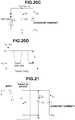
- In an arrangement in which a driver portion is directly loaded to the anode of an LD by DC coupling, as shown in
Fig. 21 , when a CMOS process is used for the driver, the voltage applied to the anode of the LD and the voltage applied to the drain of a transistor are common. - However, since the breakdown voltage of the transistor tends to decrease along with micropatterning of the recent CMOS process, in the associated shunt LD driver shown in
Fig. 21 , a voltage applied between the drain and source of the transistor exceeds the breakdown voltage, thereby undesirably breaking the transistor. - In addition, a resonant peak is present in an EO response at an LD relaxation oscillation frequency fr, and the overshooting and distortion undesirably appear in the optical waveform due to this resonant peak.
- The present invention has been made to solve these problems, and has as its object to provide a DML driving technology capable of avoiding the breakdown of the transistor.
- In order to achieve the above object, a DML driving circuit according to the present invention is a DML driving circuit including a power supply circuit configured to supply a driving current to a laser diode and a driver circuit connected in parallel to the laser diode, configured to bypass the driving current in accordance with an input modulating signal, wherein the driver circuit comprises a plurality of cascode-connected NMOS transistors, the modulating signal is applied to a gate terminal of a lowermost stage transistor located at a lowermost stage out of the NMOS transistors, and an upper stage bias potential that is a sum of a minimum gate-source voltage and a maximum drain-source voltage of a transistor located immediately below an upper stage transistor located at an upper stage above the lowermost stage transistor of the NMOS transistors is applied to a gate terminal of the upper stage transistor.
- According to the present invention, since a drain-source voltage VDS obtained when the transistor of the driving circuit is turned off can be suppressed not to exceed a maximum voltage VDSmax, the breakdown of the transistor which occurs when VDS exceeds the breakdown voltage can be avoided.
-
-
Fig. 1 is a circuit diagram showing the arrangement of a DML driving circuit according to the first embodiment; -
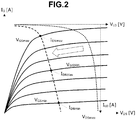
Fig. 2 is a graph showing the I-V characteristics of cascode-arranged transistors according to the first embodiment; -
Fig. 3 is a circuit diagram showing an example of a derived circuit arrangement of the DML driving circuit shown inFig. 1 ; -
Fig. 4 is a circuit diagram showing the arrangement of a DML driving circuit according to the second embodiment; -
Fig. 5 is a graph showing the I-V characteristics of a current control transistor according to the second embodiment; -
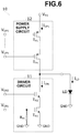
Fig. 6 is a circuit diagram showing an example of a derived circuit arrangement of the DML driving circuit shown inFig. 4 ; -
Fig. 7 is a circuit diagram sowing an example of another derived circuit arrangement of the DML driving circuit shown inFig. 4 ; -
Fig. 8 is a circuit diagram showing the arrangement of a DML driving circuit according to the third embodiment; -
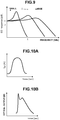
Fig. 9 is a graph showing EO responses of an LD inFig. 8 ; -
Fig. 10A is a graph showing an influence (ILD waveform) of a resonant peak on the optical waveform; -
Fig. 10B is a graph showing an influence (optical waveform) of the resonant peak on the optical waveform; -
Fig. 11 is a graph showing a compensation operation of the EO response; -
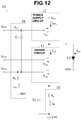
Fig. 12 is a circuit diagram showing the arrangement of a DML driving circuit according to the fourth embodiment; -
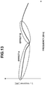
Fig. 13 is a graph showing the frequency characteristic of a driving current according to the fourth embodiment; -
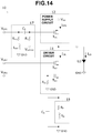
Fig. 14 is a circuit diagram showing an example of a derived circuit arrangement of the DML driving circuit shown inFig. 12 ; -
Fig. 15 is a circuit diagram showing an example of another derived circuit arrangement of the DML driving circuit shown inFig. 12 ; -
Fig. 16 is a graph showing EO responses of an LD shown inFig. 15 ; -
Fig. 17A is a graph showing an example of a large signal optical waveform (driving of an LD alone) at a relaxation oscillation frequency; -
Fig. 17B is a graph showing an example of a large signal optical waveform (LD driving by aDML driving circuit 10 inFig. 15 ); -
Fig. 18 is a block diagram of an example of the arrangement of a 100 GBase-LR4/ER4 optical transmission system; -
Fig. 19 is a circuit diagram showing an example of the arrangement of a transmission front end using a shunt LD driver; -
Fig. 20A is a circuit diagram showing an example (SW = OFF) of the circuit of the transmission front end shown inFig. 19 ; -
Fig. 20B is a timing chart showing an example (SW = OFF) of the operation of the transmission front end shown inFig. 19 ; -
Fig. 20C is a circuit diagram showing an example (SW = ON) of the circuit of the transmission front end shown inFig. 19 ; -
Fig. 20D is a timing chart showing an example (SW = ON) of the operation of the transmission front end shown inFig. 19 ; and -
Fig. 21 is a circuit diagram showing an example of the arrangement of a transmission front end using an associated shunt LD driver. - Embodiments of the present invention will now be described with reference to the accompanying drawings.
- A
DML driving circuit 10 according to the first embodiment of the present invention will be described with reference toFig. 1 . - The
DML driving circuit 10 according to this embodiment is a shunt LD driving circuit used in a transmission front end of an optical transmission system to drive a DML (Directly Modulated Laser) in which the light intensity of an LD (Laser Diode) is directly modulated. According to this embodiment, a current source load type arrangement example will be described. - As shown in
Fig. 1 , theDML driving circuit 10 according to this embodiment includes apower supply circuit 12 for supplying a driving current to an LD and adriver circuit 11 connected to the LD in parallel to bypass the driving current in accordance with an input modulating signal. According to the feature of this embodiment, the transistors of thedriver circuit 11 are two cascode-connected transistors. - The
driver circuit 11 is formed from an NMOS lowermost stage transistor TN1 located at the lower stage of the cascode connection and having the gate terminal applied with a modulating single VGN1 and the source terminal connected to a ground potential GND, and an NMOS upper stage transistor TN2 located at the upper stage of the cascode connection and having the gate terminal applied with an upper stage bias potential VGN2, the source terminal connected to the drain terminal of the transistor TN1, and the drain terminal connected to the anode terminal of the LD. - On the other hand, the
power supply circuit 12 is formed from a constant current source IS connected between a constant voltage source Vcv and the LD. The anode terminal of the LD is connected to the constant current source IS, and the cathode terminal of the LD is connected to GND. - That is, in a transmission
front end 1, the drain terminal of TN2 included in thedriver circuit 11 is directly loaded to the anode terminal of the LD. Assuming that the maximum value and the minimum value of VGN1 applied to TN1 are defined as VGN1max and VGN1min, when VGN1 is set at VGN1min, an anode-cathode voltage VLD of the LD becomes a maximum value VLDmax. - In this case, assume that drain-source voltages VDS1 and VDS2 of TN1 and TN2 are given as VDS1max and VDS2max and are divided to satisfy VDS1max = VDS2max = VLDmax/2, it is desirable that the sizes of TN1 and TN2 are equal to each other. In addition, the gate voltage VGN2 of TN2 must satisfy equation (1). When VGN2 satisfies equation (1), the gate-source voltages obtained when TN1 and TN2 are turned off become equal to each other, thereby obtaining VDS1max = VDS2max = VLDmax/2.

- A resistive element Rm connected between the gate terminal of TN1 and GND is an input matching resistor. When a 50 Ω input transmission line is used, Rm is 50 Ω. In addition, when a constant current supplied from IS, a bypass (extraction) current flowing to the
DML driving circuit 10, and the driving current flowing to the LD are defined as Ice, IDN, and ILD, respectively, ICC = IDN + ILD. - Referring to
Fig. 2 , VGSmax, VGSbias, and VGSmin are the maximum value, the bias value, and the minimum value, respectively, of the gate-source voltage VGS of the transistor. IDNmax, IDNbias, and IDNmin are the maximum current, the bias current, and the minimum current of IDN, respectively. VDSmax indicates the breakdown voltage value of the drain-source voltage of the transistor. - In the I-V characteristics of the cascode-arranged transistors according to the first embodiment, as shown in
Fig. 2 , when IDN is IDNmax, ILD becomes the minimum current value (= ILDmin). When IDN is IDNmin, ILD becomes the maximum current value (= ILDmax). A dotted line inFig. 2 indicates the I-V characteristic of the transistor when the driver is formed from only the lower stage transistor without cascode connection. Although VDS exceeds VDSmax when the transistor is turned off in case that the arrangement is formed from only the lower stage transistor, the voltage applied to the lower stage transistor is divided by the cascode arrangement, thereby obtaining the I-V characteristic indicated by a broken line. - As described above, since VDS obtained when the transistor is turned off can be suppressed not to exceed VDSmax, the breakdown of the transistor which occurs when the voltage applied between the drain and the source exceeds the breakdown voltage can be avoided.
- As an example of the arrangement of a derived circuit of the DML driving circuit shown in
Fig. 1 , a multi-stage connection example for the upper stage transistors is available, as shown inFig. 3 . The upper stage transistor TN2 is formed from a cascode arrangement of a plurality of multi-stage connected transistors TN2 to TNn. Accordingly, a voltage applied to TN1 can be reduced as compared with the two-stage arrangement. For example, by employing the n-stage cascode arrangement, a voltage applied to each stage transistor can be reduced to 1/n of the anode-cathode voltage of the LD. - A
DML driving circuit 10 according to the second embodiment of the present invention will now be described with reference toFig. 4 . In this embodiment, an example of a PMOS load type arrangement will be described. - As compared with
Fig. 1 , theDML driving circuit 10 according to the second embodiment is obtained such that a constant current source IS of apower supply circuit 12 is replaced with a PMOS current control transistor TP1 connected between a constant voltage source Vss and an LD. - As shown in
Fig. 4 , a current control bias potential VGP1 is applied to the gate terminal of TP1, the source terminal of TP1 is connected to the constant voltage source VSS, and the drain terminal of TP1 is connected to the anode terminal of the LD. When a current flowing through TP1 is given as IDP1, IDP1 = IDN + ILD. - As shown in
Fig. 5 , in the I-V characteristics of the current control transistor according to the second embodiment, since VGP1 and VSS are DC voltages, the gate-source voltage of TP1 becomes VGP1 - VSS, thereby obtaining a curve indicated by VGP1S. IDP1max and IDP1min are the maximum current value and the minimum current value, respectively. |VDS] at IDP1max is VDS21max, and |VDS| at IDP1min is VDPS1min. The LD is set off at VDSP1max and on at VDSP1min. IDP1, IDN, and ILD in the ON/OFF states of the LD satisfy equations (2) and (3) below.

- As an example of the derived circuit arrangement of the DML driving circuit shown in
Fig. 4 , a multi-stage connection example for the current control transistor TP1 shown inFig. 6 is available. A decrease in breakdown voltage due to a micropatterning process is progressing even in a PMOS transistor. To cope with this, as shown inFig. 6 , TP1 is formed from a cascode arrangement of a plurality of multi-stage connected PMOS transistors TP1 to TPn. Accordingly, a voltage applied to TP1 is divided, and the breakdown of the transistor due to an operation in which the voltage exceeds the breakdown voltage can be avoided. In this case, the multi-stage connection example of the upper stage transistor shown inFig. 3 may be applied, and the same effect as described above can be obtained. - As an example of the arrangement of another derived circuit of the DML driving circuit shown in
Fig. 4 , an example of the arrangement for suppressing voltage supply resonance shown inFig. 7 is available. In this arrangement example, as compared with the arrangement inFig. 4 , an upper stage decoupling circuit (upper stage decoupler) 13 for removing a high-frequency noise component is connected between an upper stage bias voltage VGN2 and the gate terminal of an upper stage transistor TN2. In addition, a voltage supply decoupling circuit (power supply decoupler) 14 for removing a high-frequency noise component is connected between the current control bias potential VGP1 and the gate terminal of the current control transistor TP1. - Each of the upper
stage decoupling circuit 13 and the powersupply decoupling circuit 14 is formed from an RC low-pass filter including a resistive element Rdec and a capacitive element Cdec. In addition, the decoupling capacitor Cdec is connected between the drain terminal of TN2 and GND. Note that no resistive element is added to the source terminal of TP1 because the band degrades. - Each of the upper
stage decoupling circuit 13 and the powersupply decoupling circuit 14 has the frequency characteristic of the low-pass filter having a cutoff frequency fc, as shown in equation (4). Accordingly, the high-frequency component superimposed on VGN2 and VGP1 is reduced by the upperstage decoupling circuit 13 and the powersupply decoupling circuit 14, thereby suppressing the power supply resonance caused by the high-frequency component.
- A
DML driving circuit 10 according to the third embodiment of the present invention will now be described with reference toFig. 8 . In this embodiment, an example of a high-frequency choke coil load arrangement will be described. - As compared with
Fig. 1 , theDML driving circuit 10 according to this embodiment is obtained by replacing a constant current source Is of apower supply circuit 12 with a constant voltage source Vss and a high-frequency choke coil Lc. - As shown in
Fig. 8 , one end of Lc is connected to VSS, and the other end is connected to the anode terminal of the LD. - Lc is regarded to be short-circuited upon application of a DC bias and to be open upon application of a high-frequency signal. The DC bias from Vss is applied to a
driver circuit 11 and the LD. A bypass (extraction) current IDN is modulated by a modulating current IAMP in correspondence with a voltage amplitude applied to VGN1. The modulating current of ILD is equal to IAMP. When the voltage of the modulating signal VGN1 is changed from the application of the DC bias in a direction in which an NMOS transistor TN1 is turned on, ILD decreases from ILD_bias. To the contrary, when the voltage of the modulating signal VGN1 is changed from the application of the DC bias in a direction in which an NMOS transistor TN1 is turned off, ILD increases from ILD_bias. - As shown in
Fig. 9 , the EO response of the LD ofFig. 8 has a resonant peak in the EO response at a relaxation oscillation frequency fr. The resonant peak increases when the bias current ILD_bias to the LD decreases. The overshooting and distortion occur in the optical waveform due to this resonant peak. - When ILD has a pulsed current waveform, as shown in the ILD waveform of
Fig. 10A and the optical waveform ofFig. 10B , the influence of the resonant peak on the optical waveform causes an early rise time of the optical waveform, thus obtaining an optical waveform with overshooting and distortion. In addition, the fall time is delayed. In this manner, a pulse current having a large signal amplitude is injected to the LD under the conditions in which the resonant peak is high and the bias current is small, the optical waveform becomes a waveform with overshooting and distortion while the rise time is steep and the fall time is delayed. - According to this embodiment, as shown in
Fig. 11 , the LD is driven by thedriver circuit 11 based on an ILD characteristic which cancels the resonant peak of the EO response of the LD alone, thereby reducing the influence of the resonant peak on the optical waveform at the relaxation oscillation frequency. A dotted line inFig. 11 indicates the EO response of the LD alone, and a solid line indicates the frequency characteristic of ILD when the LD is driven by a driver of this embodiment for compensating the EO response of the LD alone. A thick line is the compensated EO response. - High-frequency band compensation is performed for the frequency characteristic of ILD by the
driver circuit 11 of this embodiment in order to prevent the band of the compensated EO response from degrading more than the EO response of the LD alone. - A
DML driving circuit 10 according to the fourth embodiment of the present invention will now be described with reference toFig. 12 . In this embodiment, an example of an arrangement for compensating the optical waveform distortion caused by the resonant peak in theDML driving circuit 10 will be described. - As compared with
Fig. 4 , theDML driving circuit 10 ofFig. 12 is arranged such that aseries circuit 15 of a resistive element RE and an inductor LE is added between the source terminal of a lowermost stage NMOS transistor TN1 and a ground potential GND, and a capacitor CE is added in parallel to thisseries circuit 15. In addition, a high-pass filter 16 is added to the gate terminal of TN1 and the gate terminal of a current control transistor TP1. - The high-
pass filter 16 includes an input resistive element R1 having one end applied with a current control bias potential VGP1 and the other end connected to the gate terminal of TP1, a capacitive element C1 connected between the gate terminal of TP1 and the gate terminal of TN1, and a series circuit including a resistive element Rin and an inductor Lin and connected between the gate terminal of TN1 and GND. - Since the
series circuit 15 is formed from a series connection of RE and LE, its impedance ZRL is represented by equation (5).
- As shown in
Fig. 13 , since the impedance of theseries circuit 15 increases with an increase in frequency, the gain of ILD decreases, as shown in an effect A. By adding CE to theseries circuit 15 in parallel, the impedance of theseries circuit 15 can be reduced in a high-frequency region, as shown in an effect B, thereby increasing the gain. An impedance ZRLC obtained by adding theseries circuit 15 and CE is expressed by equation (6).
- As described, when both the
series circuit 15 and CE are applied, the effect of theseries circuit 15 is dominant up to an arbitrary frequency, thereby reducing the gain of ILD response. However, when the frequency exceeds the arbitrary frequency, the effect of CE becomes dominant, thereby increasing the gain. - As for the high-
pass filter 16, when VGP1 side is observed from the VGN1 side, the arrangement can be regarded as a high-pass filter due to the arrangement including C1 and R1. The transfer characteristic of this high-pass filter 16 can be expressed by equations (7) and (8).

- As shown in equations (7) and (8), a frequency fc becomes a cutoff frequency for the gain of ILD. As shown in the effect B of
Fig. 13 , the gain increases in the high-frequency region by the high-pass filter 16. By adding C1 and R1, the value of the input impedance in the high-frequency region changes by only the terminating resistor in the input impedance of VGN1. - For this reason, according to this embodiment, by adding the inductance Lin to the input terminating resistor Rin in series, adjustment is performed such that the input impedance is matched in a desired frequency range. Equation (9) indicates an input impedance Zin viewed from VGN1. For example, when a 50 Ω input line is used, Lin needs to be set such that Zin is set to 50 Ω in the desired frequency range.

- As an example of the arrangement of a derived circuit of the DML driving circuit shown in
Fig. 12 , an optical waveform compensation example using a high-pass filter 17 in place of the high-pass filter 16, as shown inFig. 14 , is available. - The high-
pass filter 17 includes an input capacitive element C1 having one end applied with an in-phase signal VGP1 of the modulating signal VGN1 and the other end connected to the gate terminal of the current control transistor TP1, a series circuit of a resistive element Rin1 and an inductor Lin1 connected between one end of the capacitive element C1 and a ground potential GND, and a resistive element R1 connected between a current control bias potential VGP1DC and the other end of the input capacitive element C1. - As compared with
Fig. 12 , VGP1 is an RF input signal in phase with VGN1, and given from VGP1DC, whereas the DC voltage applied to TP1 is VGP1. As inFig. 12 , the transfer characteristic and the cutoff frequency of the high-pass filter 17 are expressed by equations (10) and (11).

- As in
Fig. 12 , by adding C1 and R1, the input impedance value changes in the high-frequency region by only the terminating resistor Rin1 in the input impedance of VGP1. - For this reason, in
Fig. 14 , by adding the inductance Lin1 to the input terminating resistor Rin1 in series, adjustment is performed such that the input impedance is matched in a desired frequency range. Equation (9) indicates an input impedance Zin viewed from VGP1. For example, when a 50 Ω input line is used, Lin1 needs to be set such that Zin is set to 50 Ω in the desired frequency range.
- As an example of the arrangement of another derived circuit of the DML driving circuit shown in
Fig. 12 , an arrangement example as shown inFig. 15 is available. As compared withFig. 12 , an upperstage decoupling circuit 13, a powersupply decoupling circuit 14, and a decoupling capacitor Cdec, shown inFig. 7 , are added to the arrangement ofFig. 12 . - In other words, the upper
stage decoupling circuit 13 and the powersupply decoupling circuit 14 for suppressing the power supply resonance are connected between VGN2 and the gate terminal of TN2 and between VGP1 and the gate terminal of TP1, respectively, to which the DC voltages are applied. The decoupling capacitor Cdec for performing similar suppression is connected to the source terminal of TP1. - The capacitor Cdec of the decoupling functional portion newly added has a very large value for the input impedance Zin, the input impedance Zin is expressed by equation (9).
- When the
DML driving circuit 10 inFig. 15 is driven to equalize the bias current values to the LD, the EO response of the LD byFig. 15 is given as a graph shown inFig. 16 . In this manner, according to theDML driving circuit 10 shown inFig. 15 , it is found that the resonant peak is reduced at the relaxation oscillation frequency. - As for the example of the large signal optical waveform at the relaxation oscillation frequency,
Fig. 17A shows an optical waveform simulation result when driving is performed by the LD alone, andFig. 17B shows the optical waveform simulation degradation when LD driving is performed by theDML driving circuit 10 ofFig. 15 . As shown inFigs. 17A and 17B , it is understood that when the LD is driven by theDML driving circuit 10 shown inFig. 15 , overshooting of the optical waveform is reduced, and an eye opening becomes clear. - The present invention has been described with reference to the embodiments, but the present invention is not limited to the above embodiments. The arrangements and details of the present invention can be variously changed by those skilled in the art within the scope of the present invention. In addition, the respective embodiments may be arbitrarily combined within the consistent range.
- 10...DML driving circuit, 11...driver circuit, 12...power supply circuit, 13...upper stage decoupling circuit, 14...power supply decoupling circuit, 15...series circuit, 16, 17...high-pass filter, LD...laser diode, TN1...lowermost stage transistor, TN2 - TNn...upper stage transistor, IS...constant current source, TP1 - TPn...current control transistor, LC... high-frequency choke coil
Claims (8)
- A directly modulated laser driving circuit comprising:a power supply circuit configured to supply a driving current to a laser diode; anda driver circuit connected in parallel to the laser diode, configured to bypass the driving current in accordance with an input modulating signal,wherein the driver circuit comprises a plurality of cascode-connected NMOS transistors,the modulating signal is applied to a gate terminal of a lowermost stage transistor located at a lowermost stage out of the NMOS transistors, andan upper stage bias potential that is a sum of a minimum gate-source voltage and a maximum drain-source voltage of a transistor located immediately below an upper stage transistor located at an upper stage above the lowermost stage transistor of the NMOS transistors is applied to a gate terminal of the upper stage transistor.
- The directly modulated laser driving circuit according to claim 1, wherein the power supply circuit comprises a constant current source connected between a constant voltage source and the laser diode.
- The directly modulated laser driving circuit according to claim 1, wherein the power supply circuit includes a high-frequency choke coil connected between a constant voltage source and the laser diode.
- The directly modulated laser driving circuit according to claim 1, wherein the power supply circuit includes a PMOS current control transistor connected between a constant voltage source and the laser diode, and is configured to control the driving current to be constant based on a current control bias potential.
- The directly modulated laser driving circuit according to claim 4, further comprising:an upper stage decoupling circuit including an RC low-pass filter connected between the upper stage bias potential and the gate terminal of the upper stage transistor, and is configured to remove a high-frequency noise component;a power supply decoupling circuit including an RC low-pass filter connected between the current control bias potential and the gate terminal of the PMOS current control transistor, and is configured to remove the high-frequency noise component; anda decoupling capacitor connected between the drain terminal of the upper stage transistor and a ground potential.
- The directly modulated laser driving circuit according to claim 4, further comprising:a series circuit including a resistive element and an inductor connected between a source terminal of the lowermost stage transistor and a ground potential;a capacitor connected between the source terminal of the lowermost stage transistor and the ground potential; anda high-pass filter including an input resistive element having one end applied with the current control bias potential and the other end connected to a gate terminal of the current control transistor, a capacitive element connected between the gate terminal of the current control transistor and a gate terminal of the lowermost stage transistor, and a series circuit including a resistive element and an inductor connected between the gate terminal of the lowermost stage transistor and the ground potential.
- The directly modulated laser driving circuit according to claim 6, further comprising:an upper stage decoupling circuit including an RC low-pass filter connected between the upper stage bias potential and the gate terminal of the upper stage transistor, and is configured to remove a high-frequency noise component; anda power supply decoupling circuit including an RC low-pass filter connected between the current control bias potential and the one end of the input resistive element, and is configured to remove the high-frequency noise component.
- The directly modulated laser driving circuit according to claim 4, further comprising:a series circuit including a resistive element and an inductor connected between a source terminal of the lowermost stage transistor and a ground potential;a capacitor connected between the source terminal of the lowermost stage transistor and the ground potential; anda high-pass filter including an input capacitive element having one end applied with an in-phase signal of the modulating signal and the other end connected to a gate terminal of the current control transistor, a series circuit including a resistive element and an inductor connected between the one end of the capacitive element and the ground potential, and a resistive element connected between the current control bias potential and the other end of the capacitive element.
Applications Claiming Priority (2)
| Application Number | Priority Date | Filing Date | Title |
|---|---|---|---|
| JP2016205702 | 2016-10-20 | ||
| PCT/JP2017/037345 WO2018074410A1 (en) | 2016-10-20 | 2017-10-16 | Directly modulated laser drive circuit |
Publications (3)
| Publication Number | Publication Date |
|---|---|
| EP3531516A1 true EP3531516A1 (en) | 2019-08-28 |
| EP3531516A4 EP3531516A4 (en) | 2020-07-08 |
| EP3531516B1 EP3531516B1 (en) | 2021-08-18 |
Family
ID=62019233
Family Applications (1)
| Application Number | Title | Priority Date | Filing Date |
|---|---|---|---|
| EP17862664.4A Active EP3531516B1 (en) | 2016-10-20 | 2017-10-16 | Directly modulated laser drive circuit |
Country Status (5)
| Country | Link |
|---|---|
| US (1) | US10637207B2 (en) |
| EP (1) | EP3531516B1 (en) |
| JP (1) | JP6683825B2 (en) |
| CN (1) | CN109891690B (en) |
| WO (1) | WO2018074410A1 (en) |
Families Citing this family (19)
| Publication number | Priority date | Publication date | Assignee | Title |
|---|---|---|---|---|
| JP7215282B2 (en) * | 2019-03-26 | 2023-01-31 | 日本電信電話株式会社 | DML driver |
| US10778207B1 (en) | 2019-05-02 | 2020-09-15 | Semtech Corporation | Passive dynamic biasing for MOSFET cascode |
| CN110401103B (en) | 2019-07-26 | 2021-03-23 | 光梓信息科技(上海)有限公司 | Pulse laser driver |
| JP7275984B2 (en) * | 2019-08-09 | 2023-05-18 | オムロン株式会社 | drive circuit |
| US20230170668A1 (en) * | 2020-04-07 | 2023-06-01 | Nippon Telegraph And Telephone Corporation | DML Driver |
| WO2022163643A1 (en) * | 2021-01-28 | 2022-08-04 | パナソニックIpマネジメント株式会社 | Laser oscillator and laser processing device provided with same |
| JP7361062B2 (en) | 2021-03-25 | 2023-10-13 | 日本電信電話株式会社 | amplifier circuit |
| JP7572282B2 (en) | 2021-03-25 | 2024-10-23 | 日本電信電話株式会社 | Transmitting interface and transmitting device |
| US20240372320A1 (en) * | 2021-09-03 | 2024-11-07 | Nippon Telegraph And Telephone Corporation | Dml driver |
| JP7634695B2 (en) * | 2021-09-03 | 2025-02-21 | 日本電信電話株式会社 | DML Driver |
| CN114356131B (en) * | 2021-12-20 | 2024-06-04 | 深圳市汇顶科技股份有限公司 | Driving circuit and related electronic device |
| US11901697B2 (en) | 2022-04-05 | 2024-02-13 | Silanna Asia Pte Ltd | Single-FET pulsed laser diode driver |
| US12431686B2 (en) | 2022-04-05 | 2025-09-30 | Silanna Asia Pte Ltd | Single-FET pulsed laser diode driver |
| US20260121628A1 (en) * | 2022-04-11 | 2026-04-30 | Nippon Telegraph And Telephone Corporation | Dml driver |
| WO2024180714A1 (en) * | 2023-03-01 | 2024-09-06 | 日本電信電話株式会社 | Dml driver |
| JPWO2024209616A1 (en) * | 2023-04-06 | 2024-10-10 | ||
| US12438546B1 (en) * | 2023-06-13 | 2025-10-07 | Synopsys, Inc. | Driver/inverter using lower voltage tolerant devices |
| WO2025215734A1 (en) * | 2024-04-09 | 2025-10-16 | Ntt株式会社 | Dml driver |
| WO2025243358A1 (en) * | 2024-05-20 | 2025-11-27 | Ntt株式会社 | Multistage amplifier |
Family Cites Families (17)
| Publication number | Priority date | Publication date | Assignee | Title |
|---|---|---|---|---|
| JPH01237807A (en) * | 1988-03-18 | 1989-09-22 | Nec Corp | Semiconductor integrated circuit device |
| CA2127060A1 (en) * | 1993-06-30 | 1994-12-31 | Hiromitsu Kawamura | Modulator integrated distributed feed-back laser diode module and device using the same |
| EP0984534B1 (en) * | 1994-03-18 | 2003-06-04 | Fujitsu Limited | Drive circuit of a semiconductor optical modulator |
| US7187227B2 (en) * | 2002-08-07 | 2007-03-06 | Nippon Telegraph And Telephone Corporation | Driver circuit |
| TWI230915B (en) | 2003-10-16 | 2005-04-11 | Ind Tech Res Inst | Driving circuit of optical modulator |
| US7609734B2 (en) * | 2006-03-01 | 2009-10-27 | Intersil Americas Inc. | Switched gate current driver |
| JP2009111168A (en) * | 2007-10-30 | 2009-05-21 | Sumitomo Electric Ind Ltd | Semiconductor laser drive circuit |
| JP2010205747A (en) * | 2009-02-27 | 2010-09-16 | Sumitomo Electric Ind Ltd | Laser diode drive circuit |
| US7737790B1 (en) * | 2009-04-09 | 2010-06-15 | Mediatek Inc. | Cascode amplifier and method for controlling current of cascode amplifier |
| JP2011023474A (en) * | 2009-07-14 | 2011-02-03 | Sumitomo Electric Ind Ltd | Semiconductor laser drive circuit |
| JP2012119637A (en) * | 2010-12-03 | 2012-06-21 | Sumitomo Electric Device Innovations Inc | Manufacturing method of optical semiconductor device |
| JP6024197B2 (en) * | 2012-05-16 | 2016-11-09 | 住友電気工業株式会社 | Light emitting element drive circuit |
| JP2013251375A (en) * | 2012-05-31 | 2013-12-12 | Toshiba Corp | Optical transmission circuit and optical transmission/reception circuit module |
| US8861560B2 (en) * | 2012-11-06 | 2014-10-14 | Fujitsu Limited | Vertical-cavity surface-emitting laser driver with improved output impedance |
| JP6230429B2 (en) * | 2014-01-21 | 2017-11-15 | シャープ株式会社 | Drive circuit and touch panel device |
| JP2015216476A (en) * | 2014-05-09 | 2015-12-03 | 日本電信電話株式会社 | Driver circuit |
| CN104617483B (en) * | 2015-01-27 | 2017-06-16 | 东南大学 | The ultrahigh speed laser driver circuit and driver chip of a kind of bandwidth compensation |
-
2017
- 2017-10-16 EP EP17862664.4A patent/EP3531516B1/en active Active
- 2017-10-16 US US16/343,349 patent/US10637207B2/en active Active
- 2017-10-16 WO PCT/JP2017/037345 patent/WO2018074410A1/en not_active Ceased
- 2017-10-16 JP JP2018546320A patent/JP6683825B2/en active Active
- 2017-10-16 CN CN201780064961.0A patent/CN109891690B/en active Active
Also Published As
| Publication number | Publication date |
|---|---|
| WO2018074410A1 (en) | 2018-04-26 |
| CN109891690B (en) | 2021-02-05 |
| EP3531516B1 (en) | 2021-08-18 |
| JPWO2018074410A1 (en) | 2019-02-28 |
| US10637207B2 (en) | 2020-04-28 |
| JP6683825B2 (en) | 2020-04-22 |
| CN109891690A (en) | 2019-06-14 |
| EP3531516A4 (en) | 2020-07-08 |
| US20190245624A1 (en) | 2019-08-08 |
Similar Documents
| Publication | Publication Date | Title |
|---|---|---|
| EP3531516B1 (en) | Directly modulated laser drive circuit | |
| US20060261912A1 (en) | Radio frequency switching circuit and semiconductor device including the same | |
| US20160013614A1 (en) | Laser driver and optical module including same | |
| US20190123551A1 (en) | T-coil enhanced esd protection with passive equalization | |
| JP5071248B2 (en) | Laser diode drive circuit | |
| US9679509B2 (en) | Positive feedback enhanced switching equalizer with output pole tuning | |
| JP7634695B2 (en) | DML Driver | |
| US8571078B2 (en) | Laser driver and optical transmitter implementing the same | |
| US9825603B2 (en) | Active drain terminated distributed amplifier | |
| US20210013884A1 (en) | Differential signal transmission circuit | |
| US10666212B2 (en) | Driver circuit and optical transmitter | |
| EP2045924A1 (en) | Semiconductor circuit | |
| US20200052796A1 (en) | Optical receiver | |
| US20160254793A1 (en) | Clock and data drivers with enhanced transconductance and suppressed output common-mode | |
| US20060252394A1 (en) | Switching circuit | |
| US20140132351A1 (en) | Amplifier circuit | |
| US20230170668A1 (en) | DML Driver | |
| US20030002551A1 (en) | Laser diode driver | |
| US20040239373A1 (en) | Semiconductor laser driving circuit and optical communication apparatus | |
| WO2013175876A1 (en) | Switching amplifier, and transmitter using same | |
| US8737442B2 (en) | Driver circuit for laser diode outputting pre-emphasized signal | |
| JP7754294B2 (en) | DML Driver | |
| JP3470797B2 (en) | Buffer circuit | |
| KR20150135085A (en) | Linearizer | |
| CN105281565A (en) | Positive and negative potential generating circuit |
Legal Events
| Date | Code | Title | Description |
|---|---|---|---|
| STAA | Information on the status of an ep patent application or granted ep patent |
Free format text: STATUS: THE INTERNATIONAL PUBLICATION HAS BEEN MADE |
|
| PUAI | Public reference made under article 153(3) epc to a published international application that has entered the european phase |
Free format text: ORIGINAL CODE: 0009012 |
|
| STAA | Information on the status of an ep patent application or granted ep patent |
Free format text: STATUS: REQUEST FOR EXAMINATION WAS MADE |
|
| 17P | Request for examination filed |
Effective date: 20190409 |
|
| AK | Designated contracting states |
Kind code of ref document: A1 Designated state(s): AL AT BE BG CH CY CZ DE DK EE ES FI FR GB GR HR HU IE IS IT LI LT LU LV MC MK MT NL NO PL PT RO RS SE SI SK SM TR |
|
| AX | Request for extension of the european patent |
Extension state: BA ME |
|
| DAV | Request for validation of the european patent (deleted) | ||
| DAX | Request for extension of the european patent (deleted) | ||
| A4 | Supplementary search report drawn up and despatched |
Effective date: 20200609 |
|
| RIC1 | Information provided on ipc code assigned before grant |
Ipc: H01S 5/062 20060101ALI20200603BHEP Ipc: H01S 5/042 20060101AFI20200603BHEP Ipc: H04B 10/50 20130101ALI20200603BHEP Ipc: H03K 19/0175 20060101ALI20200603BHEP Ipc: H04B 10/54 20130101ALI20200603BHEP Ipc: H01S 5/068 20060101ALI20200603BHEP Ipc: H03F 1/22 20060101ALI20200603BHEP |
|
| GRAP | Despatch of communication of intention to grant a patent |
Free format text: ORIGINAL CODE: EPIDOSNIGR1 |
|
| STAA | Information on the status of an ep patent application or granted ep patent |
Free format text: STATUS: GRANT OF PATENT IS INTENDED |
|
| RIC1 | Information provided on ipc code assigned before grant |
Ipc: H04B 10/50 20130101ALI20210311BHEP Ipc: H01S 5/068 20060101ALI20210311BHEP Ipc: H01S 5/062 20060101ALI20210311BHEP Ipc: H04B 10/54 20130101ALI20210311BHEP Ipc: H03K 19/0175 20060101ALI20210311BHEP Ipc: H03F 1/22 20060101ALI20210311BHEP Ipc: H01S 5/042 20060101AFI20210311BHEP |
|
| INTG | Intention to grant announced |
Effective date: 20210412 |
|
| GRAS | Grant fee paid |
Free format text: ORIGINAL CODE: EPIDOSNIGR3 |
|
| GRAA | (expected) grant |
Free format text: ORIGINAL CODE: 0009210 |
|
| STAA | Information on the status of an ep patent application or granted ep patent |
Free format text: STATUS: THE PATENT HAS BEEN GRANTED |
|
| AK | Designated contracting states |
Kind code of ref document: B1 Designated state(s): AL AT BE BG CH CY CZ DE DK EE ES FI FR GB GR HR HU IE IS IT LI LT LU LV MC MK MT NL NO PL PT RO RS SE SI SK SM TR |
|
| REG | Reference to a national code |
Ref country code: GB Ref legal event code: FG4D |
|
| REG | Reference to a national code |
Ref country code: CH Ref legal event code: EP |
|
| REG | Reference to a national code |
Ref country code: DE Ref legal event code: R096 Ref document number: 602017044472 Country of ref document: DE |
|
| REG | Reference to a national code |
Ref country code: IE Ref legal event code: FG4D Ref country code: AT Ref legal event code: REF Ref document number: 1422483 Country of ref document: AT Kind code of ref document: T Effective date: 20210915 |
|
| REG | Reference to a national code |
Ref country code: LT Ref legal event code: MG9D |
|
| REG | Reference to a national code |
Ref country code: NL Ref legal event code: MP Effective date: 20210818 |
|
| REG | Reference to a national code |
Ref country code: AT Ref legal event code: MK05 Ref document number: 1422483 Country of ref document: AT Kind code of ref document: T Effective date: 20210818 |
|
| PG25 | Lapsed in a contracting state [announced via postgrant information from national office to epo] |
Ref country code: RS Free format text: LAPSE BECAUSE OF FAILURE TO SUBMIT A TRANSLATION OF THE DESCRIPTION OR TO PAY THE FEE WITHIN THE PRESCRIBED TIME-LIMIT Effective date: 20210818 Ref country code: SE Free format text: LAPSE BECAUSE OF FAILURE TO SUBMIT A TRANSLATION OF THE DESCRIPTION OR TO PAY THE FEE WITHIN THE PRESCRIBED TIME-LIMIT Effective date: 20210818 Ref country code: HR Free format text: LAPSE BECAUSE OF FAILURE TO SUBMIT A TRANSLATION OF THE DESCRIPTION OR TO PAY THE FEE WITHIN THE PRESCRIBED TIME-LIMIT Effective date: 20210818 Ref country code: ES Free format text: LAPSE BECAUSE OF FAILURE TO SUBMIT A TRANSLATION OF THE DESCRIPTION OR TO PAY THE FEE WITHIN THE PRESCRIBED TIME-LIMIT Effective date: 20210818 Ref country code: FI Free format text: LAPSE BECAUSE OF FAILURE TO SUBMIT A TRANSLATION OF THE DESCRIPTION OR TO PAY THE FEE WITHIN THE PRESCRIBED TIME-LIMIT Effective date: 20210818 Ref country code: LT Free format text: LAPSE BECAUSE OF FAILURE TO SUBMIT A TRANSLATION OF THE DESCRIPTION OR TO PAY THE FEE WITHIN THE PRESCRIBED TIME-LIMIT Effective date: 20210818 Ref country code: AT Free format text: LAPSE BECAUSE OF FAILURE TO SUBMIT A TRANSLATION OF THE DESCRIPTION OR TO PAY THE FEE WITHIN THE PRESCRIBED TIME-LIMIT Effective date: 20210818 Ref country code: BG Free format text: LAPSE BECAUSE OF FAILURE TO SUBMIT A TRANSLATION OF THE DESCRIPTION OR TO PAY THE FEE WITHIN THE PRESCRIBED TIME-LIMIT Effective date: 20211118 Ref country code: PT Free format text: LAPSE BECAUSE OF FAILURE TO SUBMIT A TRANSLATION OF THE DESCRIPTION OR TO PAY THE FEE WITHIN THE PRESCRIBED TIME-LIMIT Effective date: 20211220 Ref country code: NO Free format text: LAPSE BECAUSE OF FAILURE TO SUBMIT A TRANSLATION OF THE DESCRIPTION OR TO PAY THE FEE WITHIN THE PRESCRIBED TIME-LIMIT Effective date: 20211118 |
|
| PG25 | Lapsed in a contracting state [announced via postgrant information from national office to epo] |
Ref country code: PL Free format text: LAPSE BECAUSE OF FAILURE TO SUBMIT A TRANSLATION OF THE DESCRIPTION OR TO PAY THE FEE WITHIN THE PRESCRIBED TIME-LIMIT Effective date: 20210818 Ref country code: LV Free format text: LAPSE BECAUSE OF FAILURE TO SUBMIT A TRANSLATION OF THE DESCRIPTION OR TO PAY THE FEE WITHIN THE PRESCRIBED TIME-LIMIT Effective date: 20210818 Ref country code: GR Free format text: LAPSE BECAUSE OF FAILURE TO SUBMIT A TRANSLATION OF THE DESCRIPTION OR TO PAY THE FEE WITHIN THE PRESCRIBED TIME-LIMIT Effective date: 20211119 |
|
| PG25 | Lapsed in a contracting state [announced via postgrant information from national office to epo] |
Ref country code: NL Free format text: LAPSE BECAUSE OF FAILURE TO SUBMIT A TRANSLATION OF THE DESCRIPTION OR TO PAY THE FEE WITHIN THE PRESCRIBED TIME-LIMIT Effective date: 20210818 |
|
| PG25 | Lapsed in a contracting state [announced via postgrant information from national office to epo] |
Ref country code: DK Free format text: LAPSE BECAUSE OF FAILURE TO SUBMIT A TRANSLATION OF THE DESCRIPTION OR TO PAY THE FEE WITHIN THE PRESCRIBED TIME-LIMIT Effective date: 20210818 |
|
| REG | Reference to a national code |
Ref country code: DE Ref legal event code: R097 Ref document number: 602017044472 Country of ref document: DE |
|
| REG | Reference to a national code |
Ref country code: CH Ref legal event code: PL |
|
| PG25 | Lapsed in a contracting state [announced via postgrant information from national office to epo] |
Ref country code: SM Free format text: LAPSE BECAUSE OF FAILURE TO SUBMIT A TRANSLATION OF THE DESCRIPTION OR TO PAY THE FEE WITHIN THE PRESCRIBED TIME-LIMIT Effective date: 20210818 Ref country code: SK Free format text: LAPSE BECAUSE OF FAILURE TO SUBMIT A TRANSLATION OF THE DESCRIPTION OR TO PAY THE FEE WITHIN THE PRESCRIBED TIME-LIMIT Effective date: 20210818 Ref country code: RO Free format text: LAPSE BECAUSE OF FAILURE TO SUBMIT A TRANSLATION OF THE DESCRIPTION OR TO PAY THE FEE WITHIN THE PRESCRIBED TIME-LIMIT Effective date: 20210818 Ref country code: EE Free format text: LAPSE BECAUSE OF FAILURE TO SUBMIT A TRANSLATION OF THE DESCRIPTION OR TO PAY THE FEE WITHIN THE PRESCRIBED TIME-LIMIT Effective date: 20210818 Ref country code: CZ Free format text: LAPSE BECAUSE OF FAILURE TO SUBMIT A TRANSLATION OF THE DESCRIPTION OR TO PAY THE FEE WITHIN THE PRESCRIBED TIME-LIMIT Effective date: 20210818 Ref country code: AL Free format text: LAPSE BECAUSE OF FAILURE TO SUBMIT A TRANSLATION OF THE DESCRIPTION OR TO PAY THE FEE WITHIN THE PRESCRIBED TIME-LIMIT Effective date: 20210818 |
|
| REG | Reference to a national code |
Ref country code: BE Ref legal event code: MM Effective date: 20211031 |
|
| PLBE | No opposition filed within time limit |
Free format text: ORIGINAL CODE: 0009261 |
|
| STAA | Information on the status of an ep patent application or granted ep patent |
Free format text: STATUS: NO OPPOSITION FILED WITHIN TIME LIMIT |
|
| PG25 | Lapsed in a contracting state [announced via postgrant information from national office to epo] |
Ref country code: MC Free format text: LAPSE BECAUSE OF FAILURE TO SUBMIT A TRANSLATION OF THE DESCRIPTION OR TO PAY THE FEE WITHIN THE PRESCRIBED TIME-LIMIT Effective date: 20210818 |
|
| 26N | No opposition filed |
Effective date: 20220519 |
|
| GBPC | Gb: european patent ceased through non-payment of renewal fee |
Effective date: 20211118 |
|
| PG25 | Lapsed in a contracting state [announced via postgrant information from national office to epo] |
Ref country code: LU Free format text: LAPSE BECAUSE OF NON-PAYMENT OF DUE FEES Effective date: 20211016 Ref country code: IT Free format text: LAPSE BECAUSE OF FAILURE TO SUBMIT A TRANSLATION OF THE DESCRIPTION OR TO PAY THE FEE WITHIN THE PRESCRIBED TIME-LIMIT Effective date: 20210818 Ref country code: BE Free format text: LAPSE BECAUSE OF NON-PAYMENT OF DUE FEES Effective date: 20211031 |
|
| PG25 | Lapsed in a contracting state [announced via postgrant information from national office to epo] |
Ref country code: SI Free format text: LAPSE BECAUSE OF FAILURE TO SUBMIT A TRANSLATION OF THE DESCRIPTION OR TO PAY THE FEE WITHIN THE PRESCRIBED TIME-LIMIT Effective date: 20210818 Ref country code: LI Free format text: LAPSE BECAUSE OF NON-PAYMENT OF DUE FEES Effective date: 20211031 Ref country code: CH Free format text: LAPSE BECAUSE OF NON-PAYMENT OF DUE FEES Effective date: 20211031 |
|
| PG25 | Lapsed in a contracting state [announced via postgrant information from national office to epo] |
Ref country code: FR Free format text: LAPSE BECAUSE OF NON-PAYMENT OF DUE FEES Effective date: 20211018 |
|
| PG25 | Lapsed in a contracting state [announced via postgrant information from national office to epo] |
Ref country code: IE Free format text: LAPSE BECAUSE OF NON-PAYMENT OF DUE FEES Effective date: 20211016 Ref country code: GB Free format text: LAPSE BECAUSE OF NON-PAYMENT OF DUE FEES Effective date: 20211118 |
|
| PG25 | Lapsed in a contracting state [announced via postgrant information from national office to epo] |
Ref country code: CY Free format text: LAPSE BECAUSE OF FAILURE TO SUBMIT A TRANSLATION OF THE DESCRIPTION OR TO PAY THE FEE WITHIN THE PRESCRIBED TIME-LIMIT Effective date: 20210818 |
|
| PG25 | Lapsed in a contracting state [announced via postgrant information from national office to epo] |
Ref country code: HU Free format text: LAPSE BECAUSE OF FAILURE TO SUBMIT A TRANSLATION OF THE DESCRIPTION OR TO PAY THE FEE WITHIN THE PRESCRIBED TIME-LIMIT; INVALID AB INITIO Effective date: 20171016 |
|
| PG25 | Lapsed in a contracting state [announced via postgrant information from national office to epo] |
Ref country code: MK Free format text: LAPSE BECAUSE OF FAILURE TO SUBMIT A TRANSLATION OF THE DESCRIPTION OR TO PAY THE FEE WITHIN THE PRESCRIBED TIME-LIMIT Effective date: 20210818 |
|
| PG25 | Lapsed in a contracting state [announced via postgrant information from national office to epo] |
Ref country code: TR Free format text: LAPSE BECAUSE OF FAILURE TO SUBMIT A TRANSLATION OF THE DESCRIPTION OR TO PAY THE FEE WITHIN THE PRESCRIBED TIME-LIMIT Effective date: 20210818 |
|
| PG25 | Lapsed in a contracting state [announced via postgrant information from national office to epo] |
Ref country code: MT Free format text: LAPSE BECAUSE OF FAILURE TO SUBMIT A TRANSLATION OF THE DESCRIPTION OR TO PAY THE FEE WITHIN THE PRESCRIBED TIME-LIMIT Effective date: 20210818 |
|
| PGFP | Annual fee paid to national office [announced via postgrant information from national office to epo] |
Ref country code: DE Payment date: 20251021 Year of fee payment: 9 |
|
| REG | Reference to a national code |
Ref country code: DE Ref legal event code: R081 Ref document number: 602017044472 Country of ref document: DE Owner name: NTT, INC., JP Free format text: FORMER OWNER: NIPPON TELEGRAPH AND TELEPHONE CORPORATION, TOKYO, JP Ref country code: DE Ref legal event code: R082 Ref document number: 602017044472 Country of ref document: DE Representative=s name: DENNEMEYER & ASSOCIATES RECHTSANWALTSGESELLSCH, DE |