EP3531441A1 - A method of manufacturing semiconductor devices and corresponding semiconductor device - Google Patents
A method of manufacturing semiconductor devices and corresponding semiconductor device Download PDFInfo
- Publication number
- EP3531441A1 EP3531441A1 EP19156418.6A EP19156418A EP3531441A1 EP 3531441 A1 EP3531441 A1 EP 3531441A1 EP 19156418 A EP19156418 A EP 19156418A EP 3531441 A1 EP3531441 A1 EP 3531441A1
- Authority
- EP
- European Patent Office
- Prior art keywords
- electrically
- semiconductor die
- support member
- conductive bodies
- front surface
- Prior art date
- Legal status (The legal status is an assumption and is not a legal conclusion. Google has not performed a legal analysis and makes no representation as to the accuracy of the status listed.)
- Withdrawn
Links
Images




Classifications
-
- H—ELECTRICITY
- H10—SEMICONDUCTOR DEVICES; ELECTRIC SOLID-STATE DEVICES NOT OTHERWISE PROVIDED FOR
- H10W—GENERIC PACKAGES, INTERCONNECTIONS, CONNECTORS OR OTHER CONSTRUCTIONAL DETAILS OF DEVICES COVERED BY CLASS H10
- H10W72/00—Interconnections or connectors in packages
- H10W72/01—Manufacture or treatment
- H10W72/0198—Manufacture or treatment batch processes
-
- H—ELECTRICITY
- H10—SEMICONDUCTOR DEVICES; ELECTRIC SOLID-STATE DEVICES NOT OTHERWISE PROVIDED FOR
- H10W—GENERIC PACKAGES, INTERCONNECTIONS, CONNECTORS OR OTHER CONSTRUCTIONAL DETAILS OF DEVICES COVERED BY CLASS H10
- H10W70/00—Package substrates; Interposers; Redistribution layers [RDL]
- H10W70/01—Manufacture or treatment
- H10W70/04—Manufacture or treatment of leadframes
-
- H—ELECTRICITY
- H10—SEMICONDUCTOR DEVICES; ELECTRIC SOLID-STATE DEVICES NOT OTHERWISE PROVIDED FOR
- H10W—GENERIC PACKAGES, INTERCONNECTIONS, CONNECTORS OR OTHER CONSTRUCTIONAL DETAILS OF DEVICES COVERED BY CLASS H10
- H10W20/00—Interconnections in chips, wafers or substrates
- H10W20/01—Manufacture or treatment
- H10W20/031—Manufacture or treatment of conductive parts of the interconnections
- H10W20/056—Manufacture or treatment of conductive parts of the interconnections by filling conductive material into holes, grooves or trenches
-
- H—ELECTRICITY
- H10—SEMICONDUCTOR DEVICES; ELECTRIC SOLID-STATE DEVICES NOT OTHERWISE PROVIDED FOR
- H10W—GENERIC PACKAGES, INTERCONNECTIONS, CONNECTORS OR OTHER CONSTRUCTIONAL DETAILS OF DEVICES COVERED BY CLASS H10
- H10W20/00—Interconnections in chips, wafers or substrates
- H10W20/01—Manufacture or treatment
- H10W20/071—Manufacture or treatment of dielectric parts thereof
- H10W20/081—Manufacture or treatment of dielectric parts thereof by forming openings in the dielectric parts
-
- H—ELECTRICITY
- H10—SEMICONDUCTOR DEVICES; ELECTRIC SOLID-STATE DEVICES NOT OTHERWISE PROVIDED FOR
- H10W—GENERIC PACKAGES, INTERCONNECTIONS, CONNECTORS OR OTHER CONSTRUCTIONAL DETAILS OF DEVICES COVERED BY CLASS H10
- H10W20/00—Interconnections in chips, wafers or substrates
- H10W20/40—Interconnections external to wafers or substrates, e.g. back-end-of-line [BEOL] metallisations or vias connecting to gate electrodes
-
- H—ELECTRICITY
- H10—SEMICONDUCTOR DEVICES; ELECTRIC SOLID-STATE DEVICES NOT OTHERWISE PROVIDED FOR
- H10W—GENERIC PACKAGES, INTERCONNECTIONS, CONNECTORS OR OTHER CONSTRUCTIONAL DETAILS OF DEVICES COVERED BY CLASS H10
- H10W20/00—Interconnections in chips, wafers or substrates
- H10W20/40—Interconnections external to wafers or substrates, e.g. back-end-of-line [BEOL] metallisations or vias connecting to gate electrodes
- H10W20/41—Interconnections external to wafers or substrates, e.g. back-end-of-line [BEOL] metallisations or vias connecting to gate electrodes characterised by their conductive parts
- H10W20/42—Vias, e.g. via plugs
-
- H—ELECTRICITY
- H10—SEMICONDUCTOR DEVICES; ELECTRIC SOLID-STATE DEVICES NOT OTHERWISE PROVIDED FOR
- H10W—GENERIC PACKAGES, INTERCONNECTIONS, CONNECTORS OR OTHER CONSTRUCTIONAL DETAILS OF DEVICES COVERED BY CLASS H10
- H10W70/00—Package substrates; Interposers; Redistribution layers [RDL]
- H10W70/01—Manufacture or treatment
- H10W70/05—Manufacture or treatment of insulating or insulated package substrates, or of interposers, or of redistribution layers
- H10W70/095—Manufacture or treatment of insulating or insulated package substrates, or of interposers, or of redistribution layers of vias therein
-
- H—ELECTRICITY
- H10—SEMICONDUCTOR DEVICES; ELECTRIC SOLID-STATE DEVICES NOT OTHERWISE PROVIDED FOR
- H10W—GENERIC PACKAGES, INTERCONNECTIONS, CONNECTORS OR OTHER CONSTRUCTIONAL DETAILS OF DEVICES COVERED BY CLASS H10
- H10W70/00—Package substrates; Interposers; Redistribution layers [RDL]
- H10W70/40—Leadframes
- H10W70/421—Shapes or dispositions
-
- H—ELECTRICITY
- H10—SEMICONDUCTOR DEVICES; ELECTRIC SOLID-STATE DEVICES NOT OTHERWISE PROVIDED FOR
- H10W—GENERIC PACKAGES, INTERCONNECTIONS, CONNECTORS OR OTHER CONSTRUCTIONAL DETAILS OF DEVICES COVERED BY CLASS H10
- H10W70/00—Package substrates; Interposers; Redistribution layers [RDL]
- H10W70/60—Insulating or insulated package substrates; Interposers; Redistribution layers
- H10W70/611—Insulating or insulated package substrates; Interposers; Redistribution layers for connecting multiple chips together
- H10W70/614—Insulating or insulated package substrates; Interposers; Redistribution layers for connecting multiple chips together the multiple chips being integrally enclosed
-
- H—ELECTRICITY
- H10—SEMICONDUCTOR DEVICES; ELECTRIC SOLID-STATE DEVICES NOT OTHERWISE PROVIDED FOR
- H10W—GENERIC PACKAGES, INTERCONNECTIONS, CONNECTORS OR OTHER CONSTRUCTIONAL DETAILS OF DEVICES COVERED BY CLASS H10
- H10W70/00—Package substrates; Interposers; Redistribution layers [RDL]
- H10W70/60—Insulating or insulated package substrates; Interposers; Redistribution layers
- H10W70/62—Insulating or insulated package substrates; Interposers; Redistribution layers characterised by their interconnections
- H10W70/63—Vias, e.g. via plugs
- H10W70/635—Through-vias
-
- H—ELECTRICITY
- H10—SEMICONDUCTOR DEVICES; ELECTRIC SOLID-STATE DEVICES NOT OTHERWISE PROVIDED FOR
- H10W—GENERIC PACKAGES, INTERCONNECTIONS, CONNECTORS OR OTHER CONSTRUCTIONAL DETAILS OF DEVICES COVERED BY CLASS H10
- H10W72/00—Interconnections or connectors in packages
- H10W72/01—Manufacture or treatment
- H10W72/019—Manufacture or treatment of bond pads
-
- H—ELECTRICITY
- H10—SEMICONDUCTOR DEVICES; ELECTRIC SOLID-STATE DEVICES NOT OTHERWISE PROVIDED FOR
- H10W—GENERIC PACKAGES, INTERCONNECTIONS, CONNECTORS OR OTHER CONSTRUCTIONAL DETAILS OF DEVICES COVERED BY CLASS H10
- H10W72/00—Interconnections or connectors in packages
- H10W72/90—Bond pads, in general
-
- H—ELECTRICITY
- H10—SEMICONDUCTOR DEVICES; ELECTRIC SOLID-STATE DEVICES NOT OTHERWISE PROVIDED FOR
- H10W—GENERIC PACKAGES, INTERCONNECTIONS, CONNECTORS OR OTHER CONSTRUCTIONAL DETAILS OF DEVICES COVERED BY CLASS H10
- H10W74/00—Encapsulations, e.g. protective coatings
- H10W74/01—Manufacture or treatment
-
- H—ELECTRICITY
- H10—SEMICONDUCTOR DEVICES; ELECTRIC SOLID-STATE DEVICES NOT OTHERWISE PROVIDED FOR
- H10W—GENERIC PACKAGES, INTERCONNECTIONS, CONNECTORS OR OTHER CONSTRUCTIONAL DETAILS OF DEVICES COVERED BY CLASS H10
- H10W74/00—Encapsulations, e.g. protective coatings
- H10W74/01—Manufacture or treatment
- H10W74/016—Manufacture or treatment using moulds
-
- H—ELECTRICITY
- H10—SEMICONDUCTOR DEVICES; ELECTRIC SOLID-STATE DEVICES NOT OTHERWISE PROVIDED FOR
- H10W—GENERIC PACKAGES, INTERCONNECTIONS, CONNECTORS OR OTHER CONSTRUCTIONAL DETAILS OF DEVICES COVERED BY CLASS H10
- H10W74/00—Encapsulations, e.g. protective coatings
- H10W74/01—Manufacture or treatment
- H10W74/016—Manufacture or treatment using moulds
- H10W74/017—Auxiliary layers for moulds, e.g. release layers or layers preventing residue
-
- H—ELECTRICITY
- H10—SEMICONDUCTOR DEVICES; ELECTRIC SOLID-STATE DEVICES NOT OTHERWISE PROVIDED FOR
- H10W—GENERIC PACKAGES, INTERCONNECTIONS, CONNECTORS OR OTHER CONSTRUCTIONAL DETAILS OF DEVICES COVERED BY CLASS H10
- H10W74/00—Encapsulations, e.g. protective coatings
- H10W74/10—Encapsulations, e.g. protective coatings characterised by their shape or disposition
- H10W74/111—Encapsulations, e.g. protective coatings characterised by their shape or disposition the semiconductor body being completely enclosed
- H10W74/114—Encapsulations, e.g. protective coatings characterised by their shape or disposition the semiconductor body being completely enclosed by a substrate and the encapsulations
-
- H—ELECTRICITY
- H10—SEMICONDUCTOR DEVICES; ELECTRIC SOLID-STATE DEVICES NOT OTHERWISE PROVIDED FOR
- H10W—GENERIC PACKAGES, INTERCONNECTIONS, CONNECTORS OR OTHER CONSTRUCTIONAL DETAILS OF DEVICES COVERED BY CLASS H10
- H10W70/00—Package substrates; Interposers; Redistribution layers [RDL]
- H10W70/01—Manufacture or treatment
- H10W70/05—Manufacture or treatment of insulating or insulated package substrates, or of interposers, or of redistribution layers
-
- H—ELECTRICITY
- H10—SEMICONDUCTOR DEVICES; ELECTRIC SOLID-STATE DEVICES NOT OTHERWISE PROVIDED FOR
- H10W—GENERIC PACKAGES, INTERCONNECTIONS, CONNECTORS OR OTHER CONSTRUCTIONAL DETAILS OF DEVICES COVERED BY CLASS H10
- H10W70/00—Package substrates; Interposers; Redistribution layers [RDL]
- H10W70/01—Manufacture or treatment
- H10W70/05—Manufacture or treatment of insulating or insulated package substrates, or of interposers, or of redistribution layers
- H10W70/093—Connecting or disconnecting other interconnections thereto or therefrom, e.g. connecting bond wires or bumps
-
- H—ELECTRICITY
- H10—SEMICONDUCTOR DEVICES; ELECTRIC SOLID-STATE DEVICES NOT OTHERWISE PROVIDED FOR
- H10W—GENERIC PACKAGES, INTERCONNECTIONS, CONNECTORS OR OTHER CONSTRUCTIONAL DETAILS OF DEVICES COVERED BY CLASS H10
- H10W70/00—Package substrates; Interposers; Redistribution layers [RDL]
- H10W70/60—Insulating or insulated package substrates; Interposers; Redistribution layers
-
- H—ELECTRICITY
- H10—SEMICONDUCTOR DEVICES; ELECTRIC SOLID-STATE DEVICES NOT OTHERWISE PROVIDED FOR
- H10W—GENERIC PACKAGES, INTERCONNECTIONS, CONNECTORS OR OTHER CONSTRUCTIONAL DETAILS OF DEVICES COVERED BY CLASS H10
- H10W70/00—Package substrates; Interposers; Redistribution layers [RDL]
- H10W70/60—Insulating or insulated package substrates; Interposers; Redistribution layers
- H10W70/62—Insulating or insulated package substrates; Interposers; Redistribution layers characterised by their interconnections
- H10W70/65—Shapes or dispositions of interconnections
- H10W70/652—Cross-sectional shapes
-
- H—ELECTRICITY
- H10—SEMICONDUCTOR DEVICES; ELECTRIC SOLID-STATE DEVICES NOT OTHERWISE PROVIDED FOR
- H10W—GENERIC PACKAGES, INTERCONNECTIONS, CONNECTORS OR OTHER CONSTRUCTIONAL DETAILS OF DEVICES COVERED BY CLASS H10
- H10W70/00—Package substrates; Interposers; Redistribution layers [RDL]
- H10W70/60—Insulating or insulated package substrates; Interposers; Redistribution layers
- H10W70/62—Insulating or insulated package substrates; Interposers; Redistribution layers characterised by their interconnections
- H10W70/65—Shapes or dispositions of interconnections
- H10W70/654—Top-view layouts
- H10W70/655—Fan-out layouts
-
- H—ELECTRICITY
- H10—SEMICONDUCTOR DEVICES; ELECTRIC SOLID-STATE DEVICES NOT OTHERWISE PROVIDED FOR
- H10W—GENERIC PACKAGES, INTERCONNECTIONS, CONNECTORS OR OTHER CONSTRUCTIONAL DETAILS OF DEVICES COVERED BY CLASS H10
- H10W72/00—Interconnections or connectors in packages
- H10W72/90—Bond pads, in general
- H10W72/941—Dispositions of bond pads
- H10W72/9413—Dispositions of bond pads on encapsulations
-
- H—ELECTRICITY
- H10—SEMICONDUCTOR DEVICES; ELECTRIC SOLID-STATE DEVICES NOT OTHERWISE PROVIDED FOR
- H10W—GENERIC PACKAGES, INTERCONNECTIONS, CONNECTORS OR OTHER CONSTRUCTIONAL DETAILS OF DEVICES COVERED BY CLASS H10
- H10W74/00—Encapsulations, e.g. protective coatings
- H10W74/01—Manufacture or treatment
- H10W74/014—Manufacture or treatment using batch processing
-
- H—ELECTRICITY
- H10—SEMICONDUCTOR DEVICES; ELECTRIC SOLID-STATE DEVICES NOT OTHERWISE PROVIDED FOR
- H10W—GENERIC PACKAGES, INTERCONNECTIONS, CONNECTORS OR OTHER CONSTRUCTIONAL DETAILS OF DEVICES COVERED BY CLASS H10
- H10W74/00—Encapsulations, e.g. protective coatings
- H10W74/10—Encapsulations, e.g. protective coatings characterised by their shape or disposition
- H10W74/131—Encapsulations, e.g. protective coatings characterised by their shape or disposition the semiconductor body being only partially enclosed
- H10W74/142—Encapsulations, e.g. protective coatings characterised by their shape or disposition the semiconductor body being only partially enclosed the encapsulations exposing the passive side of the semiconductor body
-
- H—ELECTRICITY
- H10—SEMICONDUCTOR DEVICES; ELECTRIC SOLID-STATE DEVICES NOT OTHERWISE PROVIDED FOR
- H10W—GENERIC PACKAGES, INTERCONNECTIONS, CONNECTORS OR OTHER CONSTRUCTIONAL DETAILS OF DEVICES COVERED BY CLASS H10
- H10W90/00—Package configurations
Definitions
- the description relates to manufacturing semiconductor devices, such as integrated circuits (ICs).
- ICs integrated circuits
- One or more embodiments may be applied to semiconductor packages, e.g., of QFN (Quad-Flat No-Lead) type.
- QFN Quad-Flat No-Lead
- Semiconductor packaging e.g. for QFN packages, may be performed according to a number of different manufacturing methods.
- a semiconductor die may be attached to a lead frame and wire bonding may be used to connect contact pads of the semiconductor die to the leads of the lead frame.
- a flip chip method namely placing a semiconductor die on a lead frame, with the contact pads being on the surface of the semiconductor die that comes into contact with a surface of the lead frame.
- the connection to the leads of the lead frame may be obtained via solder bumps that have been deposited onto the die contact pads.
- One or more embodiments may provide such an improved solution by means of a method having the features set forth in the claims that follow.
- One or more embodiments may comprise a corresponding semiconductor device (e.g. a QFN power package).
- references to "an embodiment” or “one embodiment” in the framework of the present description is intended to indicate that a particular configuration, structure, or characteristic described in relation to the embodiment is comprised in at least one embodiment.
- phrases such as “in an embodiment” or “in one embodiment” that may be present in one or more points of the present description do not necessarily refer to one and the same embodiment.
- particular conformations, structures, or characteristics may be combined in any adequate way in one or more embodiments.
- One or more embodiments may improve over certain previous developments, e.g. MicroLeadFrame® MLF packages, for example rtMLF® (routable molded lead frame), as available with Amkor Technology - 2045 East Innovation Circle Tempe, AZ 85284, (480) 821-5000, United States, are exemplary of conventional solution.
- MicroLeadFrame® MLF packages for example rtMLF® (routable molded lead frame)
- rtMLF® routable molded lead frame
- one or more semiconductor dies 10 may be arranged on a temporary laminar support member 12, e.g. a temporary polyamide tape.
- the semiconductor dies 10 may be arranged on respective mounting locations onto a front surface 12a of the support member 12, with the mounting locations being arranged sidewise with respect to one another, optionally arranged in a row or in a matrix arrangement.
- the semiconductor dies 10 may be arranged having a back surface 10b facing the front surface 12a of the support member 12, and a front surface 10a, opposite to the back surface 10b, that may comprise one or more die pads.
- the support member 12 may comprise an adhesive tape having an adhesive front surface 12a, and the semiconductor dies 10 may be adhesively attached thereon.
- the support member 12 may comprise a UV curable layer of glue, that may act as a temporary substrate.
- the following description of one or more embodiments will refer to the manufacturing of a single semiconductor device for brevity and for the sake of understanding. However, even if described with respect to a single semiconductor device, the method may be extended to the manufacturing process of an array of packages, by adding a singulation step at the end of the method according to one or more embodiments.
- a plurality of recesses 13 may be formed in the support member 12.
- a support structure 32 e.g. a mold element of a molding tool
- the plurality of recesses of the support structure 32 may receive the back surface 12b of the support member 12, and the plurality of recesses 13 may be formed in the support member 12.
- vacuum may be applied to facilitate retaining the support member 12 on the front surface of the support structure 32.
- the back surface 12b of the support member 12 may be maintained adherent to the front surface of the support structure 32 via vacuum applied through openings 34 of the support structure 32.
- the plurality of recesses 13 may have dimensions suitable for receiving a plurality of spheres 14, as exemplified in Figure 3 .
- the spheres 14 may be dropped, i.e. placed, in corresponding recesses 13 with stencil, with the front surface 12a of the support member 12 that may facilitate maintaining the spheres 14 in the recesses 13, e.g. via adhesive attachment if the support member 12 comprises an adhesive front surface 12a.
- the plurality of spheres 14 may be arranged sidewise with respect to one another, and/or surrounding the semiconductor dies 10.
- the spheres 14 may be arranged on the temporary laminar support member 12 in a substantially concurrent step with respect to the arrangement in a row of the semiconductor dies 10.
- the spheres 14 may be arranged on the laminar support member 12 sidewise with respect to one another and surrounding the semiconductor dies 10.
- the support member 12 is an adhesive tape
- the spheres 14 and the back surfaces 10b of the semiconductor dies 10 may be attached thereto at respective mounting locations.
- rigid frames (boats) 36 may be provided, having reference holes for molding.
- the support member 12 may be held with a rigid ring.
- the support member 12 having the spheres 14 and semiconductor dies 10 attached thereon (for simplicity, only one semiconductor die 10 is visible), may be laid on the support structure 32 (e.g. a molding element of a molding tool), with the spheres 14 arranged over the plurality of recesses of the support structure 32. Again, vacuum may be applied via the openings 34, and the spheres 14 may thus form the plurality of recesses 13 of the support member 12.
- the support structure 32 e.g. a molding element of a molding tool
- the spheres 14 may be maintained in position in the recesses 13 of the support member 12, thanks to the adhesive front surface 12a thereof, if present.
- molding material may be applied to the spheres 14 and the semiconductor die 10, the molding material surrounding and optionally embedding the spheres 14 and the semiconductor die 10.
- a molding tool may be used for applying molding material to the spheres 14 and the semiconductor die 10.
- the support structure 32 may comprise a first mold part and a second mold part 38, with the first and second mold parts 32, 38 jointly defining a molding cavity C; this is merely an example of molding tool, and may vary depending on specific designs of the complementary mold parts.
- the first and second mold part may comprise plural mold elements.
- the arrangement of either Figures 3 or 6 may be enclosed in the molding cavity C, with the second molding part 38 placed over the spheres 14 and the semiconductor die 10: optionally, the spheres 14 may be clamped in the molding cavity C, i.e. in one or more embodiments, the cavity C may have a height, with respect to the plane X12, higher or equal to the height h1 of the spheres 14.
- Figure 8 represents a molding step, wherein transfer molding or sheet molding may be performed, e.g. a mold layer such as the one available with by Shin-Etsu, Asahi Seimei Otemachi Bldg., 6-1, Ohtemachi 2-chome, Chiyoda-ku, Tokyo 100-0004, Japan.
- a mold layer such as the one available with by Shin-Etsu, Asahi Seimei Otemachi Bldg., 6-1, Ohtemachi 2-chome, Chiyoda-ku, Tokyo 100-0004, Japan.
- a mold layer may be formed of molding material, e.g. laser direct structuring material LDS 30, that may surround and embed the spheres 14 and semiconductor die 10.
- An assembly 1, comprising the LDS layer 30, the spheres 14 and the semiconductor die 10 may be extracted from the molding cavity C, and the temporary support member 12 may be discarded, at least at the spheres 14.
- Figure 9 is exemplary of laser direct structuring LDS technology, that may be used to provide a routing level in one or more embodiments.
- a modified polymer 30 may be provided, comprising a metallorganic complex additive in a polymer matrix, the metallorganic complex (e.g. comprising Nitrogen, a metal element and Oxygen) being laser-activatable.
- the modified polymer 30 may comprise a LDS material, e.g. a thermoset epoxy compound.
- Laser light L radiation may be applied on the modified polymer 30, and portions 30a of the modified polymer 30, whereon the laser light L passes, may become conductive, insofar as the metallorganic complex additive comprised in the modified polymer 30 may be activated by laser ablation.
- portions a) and b) exemplify metallized LDS polymer material: in one or more embodiments, the portions 30a of the LDS material 30 may be metallized and used for routing, e.g. as electrically-conductive traces.
- Figure 11 represents a cross-sectional view of the assembly 1 after a grinding step: the LDS layer 30 may be thinner after grinding, and levelled or flattened surfaces 14a of the spheres 14 may be formed.
- Laser light may be applied to the assembly 1, thereby:
- Figure 12 exemplifies the assembly 1 after a laser exposure step and a plating step is performed: electrically-conductive material may be applied in the routing pattern written by the laser light, that may form plated traces 18.
- the traces 18 may substantially correspond to the traces 30a exemplified in Figure 10 , portions a) and b).
- a tin plating 40 may be performed, whereby portions of the spheres 14 that may be left uncovered due to the removal of the support member 12 may be plated with tin.
- Figure 13 exemplifies the possibility of providing the second mold part 38 with a protrusion 39 that may be in contact with the front surface 10a of the semiconductor die 10 when the second mold part 38 is placed over the spheres 14 and semiconductor die 10, clamps the spheres 14 and the molding cavity C is formed.
- Figure 14 represents a (e.g. transfer) molding step, wherein a mold layer 42, e.g. of STD standard epoxy, may be applied, that may embed the spheres 14 and surround the semiconductor die 10, as exemplified herein: the epoxy molding therefore may be performed exposing the front surface 10a of the semiconductor die 10.
- a mold layer 42 e.g. of STD standard epoxy
- Figure 15 represents a cross-sectional view of the assembly 1 that may be extracted from the molding cavity, after a grinding step.
- a recess 44 in a ground surface 1a may be present, due to the protrusion 39, with the front surface 10a of the semiconductor die 10 being exposed therein.
- the levelled or flattened surfaces 14a of the spheres 14 may be present at the ground surface 1a.
- a LDS layer 30 may be applied on the ground surface 1a, that may cover the levelled surfaces 14a of the spheres 14 and fill the recess 44 (thereby covering the front surface 10a of the semiconductor die 10), as exemplified in Figure 16 . If the compound used comprises LDS material 30, vias and traces can be lasered and plated, and a layer of LDS material 30 may be applied on top of the mold before grinding or after grinding.
- laser light may be applied to the LDS layer 30 and:
- Electrically-conductive plated traces 18 may thus be present within the LDS layer 30, that may be similar to the metallized portions 30a of Figure 10 , portions a) and b).
- the tin plating 40 may be present.
- Figures 18 to 21 represent cross-sectional views of semiconductor devices 100 that may be obtained with the method according to one or more embodiments.
- the semiconductor die 10 and the (e.g. ground and flattened) spheres 14 may be surrounded by molding material 42, e.g. STD epoxy material, that may be applied so that the front surface 10a of the semiconductor die 10 may be exposed.
- the back surface 10b of the semiconductor die 10 may lie in the plane X12.
- a back surface 100b of the semiconductor device 100 may lie in the plane X12, with portions of the spheres 14 protruding therefrom.
- the semiconductor die 10 which may include a silicon die, may be connected, at the die pads (not visible) thereof, via thick plated traces 18, to selected ones of the spheres 14, that may or may not be visible in the cross-sectional view of Figure 18 .
- the traces may be formed within the LDS material 30 and may have a thickness corresponding to a thickness of the LDS material 30 in portions of the LDS material away from the recess 44.
- a further molding material 46 e.g. a polymeric resist, may be applied over the plated traces 18 and the LDS material 30, to cover and protect the semiconductor device 100.
- the spheres 14 may be full, e.g. copper spheres 14', or may comprise spheres 14" that may include a polymeric material core 140 coated with electrically-conductive material 142.
- the spheres 14', 14" may be coated with tin 40 at portions extruding from the back surface 100b of the semiconductor device 100.
- Figure 19 represents a possible semiconductor device 100, similar to the semiconductor device 100 of Figure 18 , wherein also the molding material surrounding the semiconductor die 10 and ground spheres 14 may comprise LDS material 30. Accordingly, in one or more embodiments, the molding material may consist of LDS material 30, and the semiconductor die 10 and spheres 14 may be surrounded and embedded in the LDS material 30. An overmolding material may be provided on the LDS layer 30, after routing, to protect the semiconductor device 100, with the overmolding material comprising polymeric resist 46.
- a grinding step may be absent, i.e. the levelled surfaces 14a of the spheres 14 may be absent.
- the grinding step may be absent if diameters of the spheres 14 are smaller than double a thickness of the semiconductor die 10.
- the molding material e.g. epoxy material 42
- the molding material may surround the spheres 14 and the semiconductor die 10, with the epoxy material 42 having a thickness corresponding to the thickness of the semiconductor die.
- front and back portions of the spheres 14 may protrude in either direction from the molding material 42.
- the back protruding portions of the spheres 14 may be coated with tin 40.
- LDS material 30 may be applied on a front surface 42a of the molding material 42: the LDS material 30 may cover the front protruding portions of the spheres 14 and the front surface 10a of the semiconductor device 100.
- vias 48 may be formed, by laser, in the LDS material 30, at the die pads of the semiconductor die 10 and at the protruding front portions of the spheres 14.
- the vias 48 may be filled with electrically-conductive material.
- thick plated traces 18 may be formed, on the LDS material 30, between selected ones of the vias 48 at the protruding front portions of the spheres 14 and selected ones of the vias 48 at the die pads of the semiconductor die 10.
- multiple layers of LDS material 30 may be provided, e.g. a first layer 30' and a second layer 30".
- the molding material surrounding the semiconductor die 10 and the ground spheres 14 may comprise LDS material 30, or, as exemplified herein, STD epoxy material 42.
- first layer 30' may be applied on the ground surface 1a, and first vias 48' and first plated traces 18' may be formed within the first layer of LDS material 30', as previously discussed, that may connect a first set of spheres 14 and die pads.
- the second layer of LDS material 30" may be applied on a surface 1b of the first layer of LDS material 30', thereby covering the first layer of LDS material 30' and the first plated traces 18'.
- second vias 48" may be formed, that may pass through the first and second layer of LDS material 30' and 30'', towards a second set of spheres 14 and die pads.
- Second plated traces 18" may be formed within the second layer of LDS material 30", that may connect the die pads and the spheres 14 of the second set of spheres and die pads.
- the polymeric resist 46 coating may be applied, on a surface 1c of the second layer of LDS material 30", thereby covering the second layer of LDS material 30" and the second plated traces 18", and protecting the semiconductor device 100.
- Figure 21 is also exemplary of the possibility, in one or more embodiments to provide plural or multiple vias 48', 48" coupling to a "common" sphere 14. Such an arrangement may facilitate and increased current flow, e.g. in power devices.
- One or more embodiments may thus relate to the possibility of realizing a thin package in the absence of a leadframe, by using electrically-conductive (e.g. copper) bodies (e.g. spheres) or electrically-conductive bodies having a core of polymeric material plated with electrically-conductive material, e.g. copper.
- electrically-conductive bodies e.g. copper
- the electrically-conductive bodies will be exemplified and referred to as spheres, for the sake of brevity and understanding, however the spherical shape is merely a non-limiting example of possible shapes that may be used for the electrically-conductive bodies.
- the spheres may act as connections or pads for the package, after plating and connection steps are performed with die pads of a semiconductor die comprised in the package. Accordingly, plated traces may be provided, connecting the die pads and the spheres, e.g. formed on laser direct structuring LDS molding compound.
- a connection with an electrically-conductive surface of the spheres may be done on the molding compound, after a plating step may be performed on a path defined by laser writing.
- FIGS. 22 to 25 exemplify possible features of electrically-conductive bodies 14 according to one or more embodiments, wherein:
- the spheres 14 may be embedded (not visible in the figures) and/or surrounded by molding material 16, and a grinding step may be performed on a surface of the molding material in order to expose the spheres 14, and optionally form levelled front surfaces 14a of the spheres 14.
- a grinding step may be performed in a vertical direction, i.e. in a direction aligned to a z axis: for example, the grinding step may be discontinued when the levelled surfaces 14a of the spheres 14 may be formed, in the present-non limiting example the levelled surfaces 14a, that be exposed after grinding, may exemplified as dashed lines in portions a) of Figures 22 to 25 .
- the levelled front surfaces 14a may be visible, and the cores 140 of the spheres 14 - if present - may be exposed.
- trace plating steps may be performed after the spheres 14 are ground, as exemplified in portions c) of Figures 22 to 25 , wherein:
- a geometry of the traces 18 may be plated on laser direct structuring material by laser shaping.
- the electrically-conductive coating thickness may be defined in order to maintain unexposed the core 140 after grinding, depending of a shape that may be desired for connection with the spheres 14, as exemplified by the different trace profiles exemplified in portions c) of Figures 22 to 25 .
- One or more embodiments may comprise forming the respective recesses in the laminar support member by vacuum forming thereof.
- selectively removing the molding material may comprise:
- One or more embodiments may comprise filling with electrically-conductive material the passageways drilled through the molding material.
- the electrically-conductive bodies may comprise an electrically-insulating core (e.g. 140) coated with electrically-conductive material (e.g. 142).
- One or more embodiments may comprise adhesively applying the at the at least one semiconductor die and the electrically-conductive bodies at the front surface of the laminar support member.
- One or more embodiments may comprise providing the laminar support member as a tape having a plurality of semiconductor die mounting location therealong.
- One or more embodiments may comprise, after providing the filling of molding material, removing the laminar support member at least at the electrically-conductive bodies.
- One or more embodiments may relate to a semiconductor device (e.g. 100), comprising:
Landscapes
- Structures Or Materials For Encapsulating Or Coating Semiconductor Devices Or Solid State Devices (AREA)
- Encapsulation Of And Coatings For Semiconductor Or Solid State Devices (AREA)
- Engineering & Computer Science (AREA)
- Microelectronics & Electronic Packaging (AREA)
- Semiconductor Integrated Circuits (AREA)
Abstract
Description
- The description relates to manufacturing semiconductor devices, such as integrated circuits (ICs).
- One or more embodiments may be applied to semiconductor packages, e.g., of QFN (Quad-Flat No-Lead) type.
- Semiconductor packaging, e.g. for QFN packages, may be performed according to a number of different manufacturing methods.
- For example, a semiconductor die may be attached to a lead frame and wire bonding may be used to connect contact pads of the semiconductor die to the leads of the lead frame.
- Also for example, it may be possible to use a flip chip method, namely placing a semiconductor die on a lead frame, with the contact pads being on the surface of the semiconductor die that comes into contact with a surface of the lead frame. The connection to the leads of the lead frame may be obtained via solder bumps that have been deposited onto the die contact pads.
- Known package manufacturing techniques may comprise a number of disadvantages, and improved solutions are thus desirable.
- One or more embodiments may provide such an improved solution by means of a method having the features set forth in the claims that follow. One or more embodiments may comprise a corresponding semiconductor device (e.g. a QFN power package).
- The claims are an integral portion of the disclosure of the invention as provided herein.
- One or more embodiments may achieve one or more of the following results:
- assembling packages, e.g. power packages, in the absence of wire bonding step(s),
- assembling packages in the absence of a leadframe,
- improving fan-out characteristics,
- providing a package having a semiconductor die embedded therein,
- providing thick metal (e.g. copper) plating on a laser direct structuring LDS routing,
- reducing the thickness of the packages,
- the package or semiconductor device may be used for high power application, and/or
- routing may be done, upon request, by lasering.
- One or more embodiments will now be described, by way of example only, with reference to the annexed figures, wherein:
-
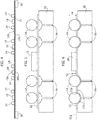
Figures 1 to 8 are exemplary of steps of a method according to one or more embodiments, -
Figures 9 and 10 , portions a) and b), are exemplary of features related to laser direct structuring technology, -
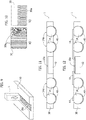
Figures 11 to 17 are exemplary of steps of a method according to one or more embodiments, -
Figures 18 to 21 represent cross-sectional views of semiconductor devices that may be manufactured with the method according to one or more embodiments, and -
Figures 22 to 25 , portions a) to c), are exemplary of possible features comprised in one or more embodiments. - By way of general remark, one may note that details and features herein discussed, singly or in combination, in connection with any one of the figures are not necessarily limited to use in embodiments as exemplified in that figure; such details and features may in fact be applied, singly or in combination, in embodiments as exemplified in any other of the figures annexed herein.
- In the ensuing description, one or more specific details are illustrated, aimed at providing an in-depth understanding of examples of embodiments of this description. The embodiments may be obtained without one or more of the specific details, or with other methods, components, materials, etc. In other cases, known structures, materials, or operations are not illustrated or described in detail so that certain aspects of embodiments will not be obscured.
- Reference to "an embodiment" or "one embodiment" in the framework of the present description is intended to indicate that a particular configuration, structure, or characteristic described in relation to the embodiment is comprised in at least one embodiment. Hence, phrases such as "in an embodiment" or "in one embodiment" that may be present in one or more points of the present description do not necessarily refer to one and the same embodiment. Moreover, particular conformations, structures, or characteristics may be combined in any adequate way in one or more embodiments.
- The references used herein are provided merely for convenience and hence do not define the extent of protection or the scope of the embodiments.
- One or more embodiments may improve over certain previous developments, e.g. MicroLeadFrame® MLF packages, for example rtMLF® (routable molded lead frame), as available with Amkor Technology - 2045 East Innovation Circle Tempe, AZ 85284, (480) 821-5000, United States, are exemplary of conventional solution.
- In one or more embodiments as exemplified in
Figure 1 , for manufacturing a semiconductor device, one or more semiconductor dies 10 may be arranged on a temporarylaminar support member 12, e.g. a temporary polyamide tape. The semiconductor dies 10 may be arranged on respective mounting locations onto afront surface 12a of thesupport member 12, with the mounting locations being arranged sidewise with respect to one another, optionally arranged in a row or in a matrix arrangement. - Accordingly, the semiconductor dies 10 may be arranged having a
back surface 10b facing thefront surface 12a of thesupport member 12, and afront surface 10a, opposite to theback surface 10b, that may comprise one or more die pads. - In one or more embodiments, the
support member 12 may comprise an adhesive tape having anadhesive front surface 12a, and the semiconductor dies 10 may be adhesively attached thereon. Alternatively, thesupport member 12 may comprise a UV curable layer of glue, that may act as a temporary substrate. - The following description of one or more embodiments will refer to the manufacturing of a single semiconductor device for brevity and for the sake of understanding. However, even if described with respect to a single semiconductor device, the method may be extended to the manufacturing process of an array of packages, by adding a singulation step at the end of the method according to one or more embodiments.
- In one or more embodiments, a plurality of
recesses 13 may be formed in thesupport member 12. As exemplified inFigure 2 , a support structure 32 (e.g. a mold element of a molding tool) may comprise a plurality of recesses on a front surface and thesupport member 12 may be laid on the front surface. The plurality of recesses of thesupport structure 32 may receive theback surface 12b of thesupport member 12, and the plurality ofrecesses 13 may be formed in thesupport member 12. - In one or more embodiments, vacuum may be applied to facilitate retaining the
support member 12 on the front surface of thesupport structure 32. For example, theback surface 12b of thesupport member 12 may be maintained adherent to the front surface of thesupport structure 32 via vacuum applied throughopenings 34 of thesupport structure 32. - In one or more embodiments, the plurality of
recesses 13 may have dimensions suitable for receiving a plurality ofspheres 14, as exemplified inFigure 3 . Thespheres 14 may be dropped, i.e. placed, incorresponding recesses 13 with stencil, with thefront surface 12a of thesupport member 12 that may facilitate maintaining thespheres 14 in therecesses 13, e.g. via adhesive attachment if thesupport member 12 comprises anadhesive front surface 12a. It will be appreciated that: - the semiconductor die 10 may lie on a plane X12, exemplified with a dashed line in
Figure 3 , - the dimensions of the
recesses 13 may be so that thespheres 14 may lie at least partially below the plane X12, i.e. in the present exemplary arrangement, portions of thespheres 14 may lie below theback surface 10b of thesemiconductor die 10, and/or - the
spheres 14 may have thickness so that, when received within therecesses 13, thespheres 14 may have a height h1 with respect to the plane X12 that exceeds a height h2 of thesemiconductor die 10 with respect to the plane X12. - In one or more embodiments, the plurality of
spheres 14 may be arranged sidewise with respect to one another, and/or surrounding the semiconductor dies 10. - In the following description of
Figures 4 to 25 , parts or elements like part or elements already introduced in connection withFigures 1 to 3 are indicated with like reference symbols, without repeating the related description for the sake of brevity. - In one or more embodiments as exemplified in the cross-sectional views of
Figures 4 to 6 , thespheres 14 may be arranged on the temporarylaminar support member 12 in a substantially concurrent step with respect to the arrangement in a row of the semiconductor dies 10. For example, thespheres 14 may be arranged on thelaminar support member 12 sidewise with respect to one another and surrounding the semiconductor dies 10. Again, if thesupport member 12 is an adhesive tape, thespheres 14 and theback surfaces 10b of the semiconductor dies 10 may be attached thereto at respective mounting locations. - In one or more embodiments, rigid frames (boats) 36 may be provided, having reference holes for molding. For example, the
support member 12 may be held with a rigid ring. - In one or more embodiments, with reference to
Figure 5 , thesupport member 12, having thespheres 14 and semiconductor dies 10 attached thereon (for simplicity, only onesemiconductor die 10 is visible), may be laid on the support structure 32 (e.g. a molding element of a molding tool), with thespheres 14 arranged over the plurality of recesses of thesupport structure 32. Again, vacuum may be applied via theopenings 34, and thespheres 14 may thus form the plurality ofrecesses 13 of thesupport member 12. - In one or more embodiments, the
spheres 14 may be maintained in position in therecesses 13 of thesupport member 12, thanks to the adhesivefront surface 12a thereof, if present. - In one or more embodiments, molding material may be applied to the
spheres 14 and the semiconductor die 10, the molding material surrounding and optionally embedding thespheres 14 and the semiconductor die 10. - For example, in one or more embodiments, as exemplified in
Figure 7 , a molding tool may be used for applying molding material to thespheres 14 and the semiconductor die 10. In the non-limiting example ofFigure 7 , thesupport structure 32 may comprise a first mold part and asecond mold part 38, with the first andsecond mold parts - In one or more embodiments, the arrangement of either
Figures 3 or6 may be enclosed in the molding cavity C, with thesecond molding part 38 placed over thespheres 14 and the semiconductor die 10: optionally, thespheres 14 may be clamped in the molding cavity C, i.e. in one or more embodiments, the cavity C may have a height, with respect to the plane X12, higher or equal to the height h1 of thespheres 14. -
Figure 8 represents a molding step, wherein transfer molding or sheet molding may be performed, e.g. a mold layer such as the one available with by Shin-Etsu, Asahi Seimei Otemachi Bldg., 6-1, Ohtemachi 2-chome, Chiyoda-ku, Tokyo 100-0004, Japan. - Therefore, a mold layer may be formed of molding material, e.g. laser direct
structuring material LDS 30, that may surround and embed thespheres 14 and semiconductor die 10. Anassembly 1, comprising theLDS layer 30, thespheres 14 and the semiconductor die 10 may be extracted from the molding cavity C, and thetemporary support member 12 may be discarded, at least at thespheres 14. - By way of background,
Figure 9 is exemplary of laser direct structuring LDS technology, that may be used to provide a routing level in one or more embodiments. - A modified
polymer 30 may be provided, comprising a metallorganic complex additive in a polymer matrix, the metallorganic complex (e.g. comprising Nitrogen, a metal element and Oxygen) being laser-activatable. In one or more embodiments, the modifiedpolymer 30 may comprise a LDS material, e.g. a thermoset epoxy compound. - Laser light L radiation may be applied on the modified
polymer 30, andportions 30a of the modifiedpolymer 30, whereon the laser light L passes, may become conductive, insofar as the metallorganic complex additive comprised in the modifiedpolymer 30 may be activated by laser ablation. -
Figure 10 , portions a) and b) exemplify metallized LDS polymer material: in one or more embodiments, theportions 30a of theLDS material 30 may be metallized and used for routing, e.g. as electrically-conductive traces. -
Figure 11 represents a cross-sectional view of theassembly 1 after a grinding step: theLDS layer 30 may be thinner after grinding, and levelled or flattenedsurfaces 14a of thespheres 14 may be formed. - Laser light may be applied to the
assembly 1, thereby: - forming vias in the
LDS layer 30 at die pads (not visible in the figures) present on thefront surface 10a of the semiconductor die 10, and - forming a routing pattern between selected ones of the
spheres 14 and selected ones of the die pads of the semiconductor die 10. -
Figure 12 exemplifies theassembly 1 after a laser exposure step and a plating step is performed: electrically-conductive material may be applied in the routing pattern written by the laser light, that may form plated traces 18. Thetraces 18 may substantially correspond to thetraces 30a exemplified inFigure 10 , portions a) and b). - In the
assembly 1 ofFigures 11 and 12 , atin plating 40 may be performed, whereby portions of thespheres 14 that may be left uncovered due to the removal of thesupport member 12 may be plated with tin. -
Figure 13 exemplifies the possibility of providing thesecond mold part 38 with aprotrusion 39 that may be in contact with thefront surface 10a of the semiconductor die 10 when thesecond mold part 38 is placed over thespheres 14 and semiconductor die 10, clamps thespheres 14 and the molding cavity C is formed. -
Figure 14 represents a (e.g. transfer) molding step, wherein amold layer 42, e.g. of STD standard epoxy, may be applied, that may embed thespheres 14 and surround the semiconductor die 10, as exemplified herein: the epoxy molding therefore may be performed exposing thefront surface 10a of the semiconductor die 10. -
Figure 15 represents a cross-sectional view of theassembly 1 that may be extracted from the molding cavity, after a grinding step. Arecess 44 in aground surface 1a may be present, due to theprotrusion 39, with thefront surface 10a of the semiconductor die 10 being exposed therein. Also, the levelled or flattenedsurfaces 14a of thespheres 14 may be present at theground surface 1a. - A
LDS layer 30 may be applied on theground surface 1a, that may cover the levelled surfaces 14a of thespheres 14 and fill the recess 44 (thereby covering thefront surface 10a of the semiconductor die 10), as exemplified inFigure 16 . If the compound used comprisesLDS material 30, vias and traces can be lasered and plated, and a layer ofLDS material 30 may be applied on top of the mold before grinding or after grinding. - Again, with reference to
Figure 17 , laser light may be applied to theLDS layer 30 and: - vias may be formed in the
LDS layer 30 at levelledsurfaces 14a of thespheres 14 and at die pads (not visible) on thefront surface 10a of the semiconductor die 10, - routes may be formed between selected ones of the
spheres 14 and selected ones of the die pads of the semiconductor die 10, and - electrically-conductive material may be applied to the routes and vias written by the laser.
- Electrically-conductive plated traces 18 may thus be present within the
LDS layer 30, that may be similar to the metallizedportions 30a ofFigure 10 , portions a) and b). - Also in the
assembly 1 ofFigures 15 to 17 , the tin plating 40 may be present. -
Figures 18 to 21 represent cross-sectional views ofsemiconductor devices 100 that may be obtained with the method according to one or more embodiments. The semiconductor die 10 and the (e.g. ground and flattened)spheres 14 may be surrounded by moldingmaterial 42, e.g. STD epoxy material, that may be applied so that thefront surface 10a of the semiconductor die 10 may be exposed. Theback surface 10b of the semiconductor die 10 may lie in the plane X12. Also aback surface 100b of thesemiconductor device 100 may lie in the plane X12, with portions of thespheres 14 protruding therefrom. - In
Figure 18 , the semiconductor die 10, which may include a silicon die, may be connected, at the die pads (not visible) thereof, via thick plated traces 18, to selected ones of thespheres 14, that may or may not be visible in the cross-sectional view ofFigure 18 . The traces may be formed within theLDS material 30 and may have a thickness corresponding to a thickness of theLDS material 30 in portions of the LDS material away from therecess 44. - A
further molding material 46, e.g. a polymeric resist, may be applied over the plated traces 18 and theLDS material 30, to cover and protect thesemiconductor device 100. In one or more embodiments, as exemplified inFigure 18 , thespheres 14 may be full, e.g. copper spheres 14', or may comprisespheres 14" that may include apolymeric material core 140 coated with electrically-conductive material 142. Thespheres 14', 14" may be coated withtin 40 at portions extruding from theback surface 100b of thesemiconductor device 100. -
Figure 19 represents apossible semiconductor device 100, similar to thesemiconductor device 100 ofFigure 18 , wherein also the molding material surrounding the semiconductor die 10 andground spheres 14 may compriseLDS material 30. Accordingly, in one or more embodiments, the molding material may consist ofLDS material 30, and the semiconductor die 10 andspheres 14 may be surrounded and embedded in theLDS material 30. An overmolding material may be provided on theLDS layer 30, after routing, to protect thesemiconductor device 100, with the overmolding material comprising polymeric resist 46. - In one or more embodiments, as exemplified in
Figure 20 , a grinding step may be absent, i.e. the levelled surfaces 14a of thespheres 14 may be absent. For example, the grinding step may be absent if diameters of thespheres 14 are smaller than double a thickness of the semiconductor die 10. - The molding material, e.g.
epoxy material 42, may surround thespheres 14 and the semiconductor die 10, with theepoxy material 42 having a thickness corresponding to the thickness of the semiconductor die. In particular, front and back portions of thespheres 14 may protrude in either direction from themolding material 42. On theback surface 100b of thesemiconductor device 100, the back protruding portions of thespheres 14 may be coated withtin 40. Conversely,LDS material 30 may be applied on afront surface 42a of the molding material 42: theLDS material 30 may cover the front protruding portions of thespheres 14 and thefront surface 10a of thesemiconductor device 100. - In one or more embodiments, vias 48 may be formed, by laser, in the
LDS material 30, at the die pads of the semiconductor die 10 and at the protruding front portions of thespheres 14. Thevias 48 may be filled with electrically-conductive material. - In one or more embodiments, thick plated traces 18 may be formed, on the
LDS material 30, between selected ones of the vias 48 at the protruding front portions of thespheres 14 and selected ones of the vias 48 at the die pads of the semiconductor die 10. - In one or more embodiments, as exemplified in
Figure 21 , multiple layers ofLDS material 30 may be provided, e.g. a first layer 30' and asecond layer 30". Also, the molding material surrounding the semiconductor die 10 and theground spheres 14 may compriseLDS material 30, or, as exemplified herein,STD epoxy material 42. - For example, the first layer 30' may be applied on the
ground surface 1a, andfirst vias 48' and first plated traces 18' may be formed within the first layer of LDS material 30', as previously discussed, that may connect a first set ofspheres 14 and die pads. - The second layer of
LDS material 30" may be applied on asurface 1b of the first layer of LDS material 30', thereby covering the first layer of LDS material 30' and the first plated traces 18'. Similarly,second vias 48" may be formed, that may pass through the first and second layer of LDS material 30' and 30'', towards a second set ofspheres 14 and die pads. Second plated traces 18" may be formed within the second layer ofLDS material 30", that may connect the die pads and thespheres 14 of the second set of spheres and die pads. - Again, the polymeric resist 46 coating may be applied, on a
surface 1c of the second layer ofLDS material 30", thereby covering the second layer ofLDS material 30" and the second plated traces 18", and protecting thesemiconductor device 100. -
Figure 21 is also exemplary of the possibility, in one or more embodiments to provide plural ormultiple vias sphere 14. Such an arrangement may facilitate and increased current flow, e.g. in power devices. - One or more embodiments may thus relate to the possibility of realizing a thin package in the absence of a leadframe, by using electrically-conductive (e.g. copper) bodies (e.g. spheres) or electrically-conductive bodies having a core of polymeric material plated with electrically-conductive material, e.g. copper. Hereinafter, the electrically-conductive bodies will be exemplified and referred to as spheres, for the sake of brevity and understanding, however the spherical shape is merely a non-limiting example of possible shapes that may be used for the electrically-conductive bodies.
- In one or more embodiments, the spheres may act as connections or pads for the package, after plating and connection steps are performed with die pads of a semiconductor die comprised in the package. Accordingly, plated traces may be provided, connecting the die pads and the spheres, e.g. formed on laser direct structuring LDS molding compound.
- In one or more embodiments, a connection with an electrically-conductive surface of the spheres may be done on the molding compound, after a plating step may be performed on a path defined by laser writing.
-
Figures 22 to 25 exemplify possible features of electrically-conductive bodies 14 according to one or more embodiments, wherein: -
Figure 22 exemplifies afull sphere 14 made of copper alloy, -
Figure 23 exemplifies ametallic core 140 coated with electrically-conductive material 142, e.g. copper, -
figure 24 exemplifies a polymeric, e.g. PTFE, polytetrafluoroethylene -core 140 coated with electrically-conductive material 142, -
Figure 25 exemplifies a polymeric, e.g. a laser direct structuring LDS material,core 140 coated with an electrically-conductive material 142, and wherein: - portions a) exemplify cross-sectional views of the
spheres 14, - portions b) exemplify top views of the
spheres 14 after grinding steps are performed thereon, and - portions c) exemplify top views of the
spheres 14 after trace plating steps are performed. - In one or more embodiments, as exemplified in portions b) of
Figures 22 to 25 , thespheres 14 may be embedded (not visible in the figures) and/or surrounded by moldingmaterial 16, and a grinding step may be performed on a surface of the molding material in order to expose thespheres 14, and optionally form levelledfront surfaces 14a of thespheres 14. - For example, considering an x-y-z Cartesian system as exemplified in
Figures 22 to 25 , a grinding step may be performed in a vertical direction, i.e. in a direction aligned to a z axis: for example, the grinding step may be discontinued when the levelled surfaces 14a of thespheres 14 may be formed, in the present-non limiting example the levelledsurfaces 14a, that be exposed after grinding, may exemplified as dashed lines in portions a) ofFigures 22 to 25 . - Accordingly, in the top views of portions b) of
Figures 22 to 25 , the levelledfront surfaces 14a may be visible, and thecores 140 of the spheres 14 - if present - may be exposed. - In one or more embodiments, trace plating steps may be performed after the
spheres 14 are ground, as exemplified in portions c) ofFigures 22 to 25 , wherein: - a
trace 18 may extend to a peripheral portion of thesphere 14, as exemplified inFigure 22 portion c), - a
trace 18 may extend to cover the entire levelledsurface 14a of thesphere 14, as exemplified inFigure 23 portion c), - a
trace 18 may extend to a peripheral portion of thesphere 14, leaving exposed thecore 140, as exemplified inFigure 24 portion c), and - a
linear trace 18 may extend across thesphere 14 reaching two opposite ends of thecoated portion 142 thereof, as exemplified inFigure 25 portion c). - It will be appreciated that a geometry of the
traces 18 may be plated on laser direct structuring material by laser shaping. - In one or more embodiments, a sphere thickness may be comprised in a range of 100 µm to 500 µm (1 µm = 10- 6 m), which may be related to a package body thickness and a semiconductor die thickness. In one or more embodiments, if the
spheres 14 are coated with electrically-conductive material 142, e.g. copper plated polymer spheres, the electrically-conductive coating thickness may be defined in order to maintain unexposed the core 140 after grinding, depending of a shape that may be desired for connection with thespheres 14, as exemplified by the different trace profiles exemplified in portions c) ofFigures 22 to 25 . - One or more embodiments may thus relate to a method that may comprise:
- providing a laminar support member (e.g. 12), having a front surface (e.g. 12a) and a back surface (e.g. 12b) with at least one semiconductor die mounting location lying in a plane (e.g. X12) at the front surface of the support member,
- arranging at the at least one semiconductor die mounting location lying in the plane at least one semiconductor die (e.g. 10) having a front surface (e.g. 10a) and a back surface (e.g. 10b) with the back surface of the at least one semiconductor die towards the front surface of the support member, the at least one semiconductor die having die pads at the front surface thereof,
- arranging at the front surface of the support member sidewise of the at least one semiconductor die mounting location a plurality of electrically-conductive bodies (e.g. 14), the electrically-conductive bodies arranged at respective recesses (e.g. 13) in the support member, the respective recesses opening at the front surface of the support member,
- providing a filling of molding material (e.g. 30, 42, 46) over the laminar support member between the at least one semiconductor die and the electrically-conductive bodies, and
- providing electrically-conductive lines (e.g. 18) between selected ones of the die pads of the semiconductor die and selected ones of the plurality of electrically-conductive bodies.
- One or more embodiments may comprise:
- forming respective recesses in the laminar support member and arranging the electrically-conductive bodies into the recesses formed in the laminar support member; or
- arranging the electrically-conductive bodies at the front surface of the support member and causing the electrically-conductive bodies to advance into the support member with respective recesses provided therein.
- One or more embodiments may comprise forming the respective recesses in the laminar support member by vacuum forming thereof.
- One or more embodiments may comprise:
- providing the electrically-conductive lines extending over the filling of molding material between the at least one semiconductor die and the electrically-conductive bodies, and
- providing at least one further filling of molding material (e.g. 30, 42, 46) covering the electrically-conductive lines, the front surface of the at least one semiconductor die and the electrically-conductive bodies.
- One or more embodiments may comprise:
- dispensing the filling of molding material over the laminar support member by covering the at least one semiconductor die and the electrically-conductive bodies,
- providing electrically contact surfaces for the electrically-conductive lines at said selected ones of the die pads of the semiconductor die and selected ones of the plurality of electrically-conductive bodies by:
- selectively removing the molding material at the selected ones of the die pads of the semiconductor die and/or selected ones of the plurality of electrically-conductive bodies, and/or
- including laser direct structuring material (e.g. 30) in the molding material at said selected ones of the die pads of the semiconductor die and/or selected ones of the plurality of electrically-conductive bodies and laser activating (e.g. L) the laser direct structuring material at said selected ones of the die pads of the semiconductor die and/or selected ones of the plurality of electrically-conductive bodies.
- In one or more embodiments, selectively removing the molding material may comprise:
- drilling passageways (e.g. 48) through the molding material, and/or
- grinding the molding material.
- One or more embodiments may comprise filling with electrically-conductive material the passageways drilled through the molding material.
- In one or more embodiments, the electrically-conductive bodies may comprise an electrically-insulating core (e.g. 140) coated with electrically-conductive material (e.g. 142).
- One or more embodiments may comprise adhesively applying the at the at least one semiconductor die and the electrically-conductive bodies at the front surface of the laminar support member.
- One or more embodiments may comprise providing the laminar support member as a tape having a plurality of semiconductor die mounting location therealong.
- One or more embodiments may comprise, after providing the filling of molding material, removing the laminar support member at least at the electrically-conductive bodies.
- One or more embodiments may relate to a semiconductor device (e.g. 100), comprising:
- at least one semiconductor die (e.g. 10), the at least one semiconductor die having a front surface (e.g. 10a) and a back surface (e.g. 10b) lying in plane (e.g. X12), the at least one semiconductor die having die pads at the front surface thereof,
- a plurality of electrically-conductive bodies (e.g. 14), the electrically-conductive bodies arranged sidewise of the at least one semiconductor die and protruding from the plane away from the back surface of the at least one semiconductor die, opposite the at least one semiconductor die,
- a filling of molding material (e.g. 30, 42, 46) between the at least one semiconductor die and the electrically-conductive bodies, and
- electrically-conductive lines (e.g. 18) between selected ones of the die pads of the semiconductor die and selected ones of the plurality of electrically-conductive bodies, the semiconductor device obtainable with the method according to one or more embodiments.
- Without prejudice to the underlying principles, the details and embodiments may vary, even significantly, with respect to what has been disclosed by way of example only, without departing from the extent of protection.
- In that respect, one may again note that details and features herein discussed, singly or in combination, in connection with any one of the figures are not necessarily limited to use in embodiments as exemplified in that figure; such details and features may in fact be applied, singly or in combination, in embodiments as exemplified in any other of the figures annexed herein.
- The extent of protection is defined by the annexed claims.
Claims (12)
- A method, comprising:- providing a laminar support member (12) having a front surface (12a) and a back surface (12b) with at least one semiconductor die mounting location lying in a plane (X12) at the front surface (12a) of the support member (12),- arranging at the at least one semiconductor die mounting location lying in said plane (X12) at least one semiconductor die (10) having a front surface (10a) and a back surface (10b) with the back surface (10b) of the at least one semiconductor die (10) towards the front surface (12a) of the support member (12), the at least one semiconductor die (10) having die pads at the front surface (10a) thereof,- arranging at the front surface (12a) of the support member (12) sidewise of the at least one semiconductor die mounting location a plurality of electrically-conductive bodies (14), the electrically-conductive bodies (14) arranged at respective recesses (13) in the support member (12), the respective recesses (13) opening at the front surface (12a) of the support member (12),- providing a filling of molding material (30, 42, 46) over the laminar support member (12) between the at least one semiconductor die (10) and the electrically-conductive bodies (14), and- providing electrically-conductive lines (18) between selected ones of the die pads of the semiconductor die (10) and selected ones of the plurality of electrically-conductive bodies (14).
- The method of claim 1, comprising:- forming respective recesses (13) in the laminar support member (12) and arranging the electrically-conductive bodies (14) into the recesses (13) formed in the laminar support member (12); or- arranging the electrically-conductive bodies (14) at the front surface (12a) of the support member (12) and causing the electrically-conductive bodies (14) to advance into the support member (12) with respective recesses (13) provided therein.
- The method of claim 1 or claim 2, comprising forming the respective recesses (13) in the laminar support member (12) by vacuum forming thereof.
- The method of any of the previous claims, comprising:- providing said electrically-conductive lines (18) extending over the filling of molding material (30, 42, 46) between the at least one semiconductor die (10) and the electrically-conductive bodies (14), and- providing at least one further filling of molding material (30, 42, 46) covering the electrically-conductive lines (18), the front surface (10a) of the at least one semiconductor die (10) and the electrically-conductive bodies (14).
- The method of any of the previous claims, comprising:- dispensing the filling of molding material (30, 42, 46) over the laminar support member (12) by covering the at least one semiconductor die (10) and the electrically-conductive bodies (14),- providing electrically contact surfaces for the electrically-conductive lines (18) at said selected ones of the die pads of the semiconductor die (10) and selected ones of the plurality of electrically-conductive bodies (14) by:- selectively removing the molding material (30, 42, 46) at said selected ones of the die pads of the semiconductor die (10) and/or selected ones of the plurality of electrically-conductive bodies (14), and/or- including laser direct structuring material (30) in the molding material (30, 42, 46) at said selected ones of the die pads of the semiconductor die (10) and/or selected ones of the plurality of electrically-conductive bodies (14) and laser activating (L) the laser direct structuring material (30) at said selected ones of the die pads of the semiconductor die (10) and/or selected ones of the plurality of electrically-conductive bodies (14).
- The method of claim 5, wherein selectively removing the molding material (30, 42, 46) comprises:- drilling passageways (48) through the molding material (30, 42, 46), and/or- grinding the molding material (30, 42, 46).
- The method of claim 6 comprising filling with electrically-conductive material the passageways (48) drilled through the molding material (30, 42, 46).
- The method of any of the previous claims, wherein the electrically-conductive bodies (14) comprise an electrically-insulating core (140) coated with electrically-conductive material (142).
- The method of any of the previous claims, comprising adhesively applying the at the at least one semiconductor die (10) and the electrically-conductive bodies (14) at the front surface (12a) of the laminar support member (12).
- The method of any of the previous claims, comprising providing the laminar support member (12) as a tape having a plurality of semiconductor die mounting location therealong.
- The method of any of the previous claims, comprising, after providing the filling of molding material (30, 42, 46), removing the laminar support member (12) at least at the electrically-conductive bodies (14).
- A semiconductor device (100), comprising:- at least one semiconductor die (10), the at least one semiconductor die (10) having a front surface (10a) and a back surface (10b) lying in plane (X12), the at least one semiconductor die (10) having die pads at the front surface (10a) thereof,- a plurality of electrically-conductive bodies (14), the electrically-conductive bodies (14) arranged sidewise of the at least one semiconductor die (10) and protruding from said plane (X12) opposite the at least one semiconductor die (10),- a filling of molding material (30, 42, 46) between the at least one semiconductor die (10) and the electrically-conductive bodies (14), and- electrically-conductive lines (18) between selected ones of the die pads of the semiconductor die (10) and selected ones of the plurality of electrically-conductive bodies (14).
Applications Claiming Priority (1)
| Application Number | Priority Date | Filing Date | Title |
|---|---|---|---|
| IT102018000002903A IT201800002903A1 (en) | 2018-02-21 | 2018-02-21 | PROCEDURE FOR MANUFACTURING SEMICONDUCTOR DEVICES AND CORRESPONDING SEMICONDUCTOR DEVICE |
Publications (1)
| Publication Number | Publication Date |
|---|---|
| EP3531441A1 true EP3531441A1 (en) | 2019-08-28 |
Family
ID=62089982
Family Applications (1)
| Application Number | Title | Priority Date | Filing Date |
|---|---|---|---|
| EP19156418.6A Withdrawn EP3531441A1 (en) | 2018-02-21 | 2019-02-11 | A method of manufacturing semiconductor devices and corresponding semiconductor device |
Country Status (4)
| Country | Link |
|---|---|
| US (1) | US10971375B2 (en) |
| EP (1) | EP3531441A1 (en) |
| CN (2) | CN110176404A (en) |
| IT (1) | IT201800002903A1 (en) |
Cited By (2)
| Publication number | Priority date | Publication date | Assignee | Title |
|---|---|---|---|---|
| DE102020108851B4 (en) | 2019-04-04 | 2023-03-16 | Infineon Technologies Ag | THE-TO-WIRE CONNECTION IN THE PACKAGING OF A MOLDED SEMICONDUCTOR HOUSING AND METHOD FOR ITS MANUFACTURE |
| US12021052B2 (en) | 2020-01-29 | 2024-06-25 | Stmicroelectronics S.R.L. | Method of manufacturing semiconductor products, semiconductor product, device and testing method |
Families Citing this family (11)
| Publication number | Priority date | Publication date | Assignee | Title |
|---|---|---|---|---|
| IT201700073501A1 (en) * | 2017-06-30 | 2018-12-30 | St Microelectronics Srl | SEMICONDUCTOR PRODUCT AND CORRESPONDENT PROCEDURE |
| US10741466B2 (en) | 2017-11-17 | 2020-08-11 | Infineon Technologies Ag | Formation of conductive connection tracks in package mold body using electroless plating |
| KR102605122B1 (en) | 2017-12-08 | 2023-11-24 | 인피니언 테크놀로지스 아게 | Semiconductor package with air cavity |
| IT201800002903A1 (en) * | 2018-02-21 | 2019-08-21 | St Microelectronics Srl | PROCEDURE FOR MANUFACTURING SEMICONDUCTOR DEVICES AND CORRESPONDING SEMICONDUCTOR DEVICE |
| US11133281B2 (en) | 2019-04-04 | 2021-09-28 | Infineon Technologies Ag | Chip to chip interconnect in encapsulant of molded semiconductor package |
| CN112018052A (en) | 2019-05-31 | 2020-12-01 | 英飞凌科技奥地利有限公司 | Semiconductor package with laser activatable molding compound |
| US11587800B2 (en) | 2020-05-22 | 2023-02-21 | Infineon Technologies Ag | Semiconductor package with lead tip inspection feature |
| US12519046B2 (en) * | 2021-03-02 | 2026-01-06 | Stmicroelectronics Pte Ltd | Wafer level packaging having redistribution layer formed utilizing laser direct structuring |
| US12080631B2 (en) * | 2021-08-31 | 2024-09-03 | Stmicroelectronics S.R.L. | Leadframe-less laser direct structuring (LDS) package |
| FR3131977A1 (en) * | 2022-01-20 | 2023-07-21 | Stmicroelectronics (Tours) Sas | Manufacture of electronic components |
| US12599004B2 (en) | 2022-09-28 | 2026-04-07 | Nxp Usa, Inc. | Semiconductor device with active mold package and method therefor |
Citations (7)
| Publication number | Priority date | Publication date | Assignee | Title |
|---|---|---|---|---|
| US20010002330A1 (en) * | 1999-04-03 | 2001-05-31 | Benenati Joseph A. | Rolling ball connector |
| US20070190690A1 (en) * | 2006-02-14 | 2007-08-16 | Stats Chippac Ltd. | Integrated circuit package system with exposed interconnects |
| US20090102066A1 (en) * | 2007-10-22 | 2009-04-23 | Advanced Semiconductor Engineering, Inc. | Chip package structure and method of manufacturing the same |
| US20100072599A1 (en) * | 2008-09-22 | 2010-03-25 | Stats Chippac, Ltd. | Semiconductor Device and Method of Forming a Wafer Level Package with Top and Bottom Solder Bump Interconnection |
| US20100127386A1 (en) * | 2008-11-26 | 2010-05-27 | Infineon Technologies Ag | Device including a semiconductor chip |
| US20130105991A1 (en) * | 2011-11-02 | 2013-05-02 | Stmicroelectronics Pte Ltd. | Embedded wafer level package for 3d and package-on-package applications, and method of manufacture |
| US20170345764A1 (en) * | 2016-05-24 | 2017-11-30 | Taiwan Semiconductor Manufacturing Co., Ltd. | Integrated fan-out package and method of fabricating the same |
Family Cites Families (13)
| Publication number | Priority date | Publication date | Assignee | Title |
|---|---|---|---|---|
| TW466723B (en) * | 2000-12-01 | 2001-12-01 | Siliconware Precision Industries Co Ltd | Super thin package having high heat-dissipation property |
| US8237259B2 (en) * | 2007-06-13 | 2012-08-07 | Infineon Technologies Ag | Embedded chip package |
| US8390107B2 (en) * | 2007-09-28 | 2013-03-05 | Intel Mobile Communications GmbH | Semiconductor device and methods of manufacturing semiconductor devices |
| US7888181B2 (en) * | 2008-09-22 | 2011-02-15 | Stats Chippac, Ltd. | Method of forming a wafer level package with RDL interconnection over encapsulant between bump and semiconductor die |
| US8105915B2 (en) * | 2009-06-12 | 2012-01-31 | Stats Chippac, Ltd. | Semiconductor device and method of forming vertical interconnect structure between non-linear portions of conductive layers |
| US8546193B2 (en) * | 2010-11-02 | 2013-10-01 | Stats Chippac, Ltd. | Semiconductor device and method of forming penetrable film encapsulant around semiconductor die and interconnect structure |
| US8922013B2 (en) * | 2011-11-08 | 2014-12-30 | Stmicroelectronics Pte Ltd. | Through via package |
| US8878360B2 (en) * | 2012-07-13 | 2014-11-04 | Intel Mobile Communications GmbH | Stacked fan-out semiconductor chip |
| US9425178B2 (en) * | 2014-07-08 | 2016-08-23 | Taiwan Semiconductor Manufacturing Company, Ltd. | RDL-first packaging process |
| US9461009B1 (en) * | 2015-05-27 | 2016-10-04 | Freescale Semiconductor, Inc. | Method and apparatus for assembling a semiconductor package |
| US20180096975A1 (en) * | 2016-09-30 | 2018-04-05 | Intel Corporation | High density package on package devices created through a self assembly monolayer assisted laser direct structuring process on mold compound |
| US10818578B2 (en) * | 2017-10-12 | 2020-10-27 | Stmicroelectronics S.R.L. | Method of manufacturing semiconductor devices, corresponding device and circuit |
| IT201800002903A1 (en) * | 2018-02-21 | 2019-08-21 | St Microelectronics Srl | PROCEDURE FOR MANUFACTURING SEMICONDUCTOR DEVICES AND CORRESPONDING SEMICONDUCTOR DEVICE |
-
2018
- 2018-02-21 IT IT102018000002903A patent/IT201800002903A1/en unknown
-
2019
- 2019-02-11 EP EP19156418.6A patent/EP3531441A1/en not_active Withdrawn
- 2019-02-12 US US16/273,991 patent/US10971375B2/en active Active
- 2019-02-20 CN CN201910127244.9A patent/CN110176404A/en active Pending
- 2019-02-20 CN CN201920222984.6U patent/CN209592023U/en active Active
Patent Citations (7)
| Publication number | Priority date | Publication date | Assignee | Title |
|---|---|---|---|---|
| US20010002330A1 (en) * | 1999-04-03 | 2001-05-31 | Benenati Joseph A. | Rolling ball connector |
| US20070190690A1 (en) * | 2006-02-14 | 2007-08-16 | Stats Chippac Ltd. | Integrated circuit package system with exposed interconnects |
| US20090102066A1 (en) * | 2007-10-22 | 2009-04-23 | Advanced Semiconductor Engineering, Inc. | Chip package structure and method of manufacturing the same |
| US20100072599A1 (en) * | 2008-09-22 | 2010-03-25 | Stats Chippac, Ltd. | Semiconductor Device and Method of Forming a Wafer Level Package with Top and Bottom Solder Bump Interconnection |
| US20100127386A1 (en) * | 2008-11-26 | 2010-05-27 | Infineon Technologies Ag | Device including a semiconductor chip |
| US20130105991A1 (en) * | 2011-11-02 | 2013-05-02 | Stmicroelectronics Pte Ltd. | Embedded wafer level package for 3d and package-on-package applications, and method of manufacture |
| US20170345764A1 (en) * | 2016-05-24 | 2017-11-30 | Taiwan Semiconductor Manufacturing Co., Ltd. | Integrated fan-out package and method of fabricating the same |
Cited By (2)
| Publication number | Priority date | Publication date | Assignee | Title |
|---|---|---|---|---|
| DE102020108851B4 (en) | 2019-04-04 | 2023-03-16 | Infineon Technologies Ag | THE-TO-WIRE CONNECTION IN THE PACKAGING OF A MOLDED SEMICONDUCTOR HOUSING AND METHOD FOR ITS MANUFACTURE |
| US12021052B2 (en) | 2020-01-29 | 2024-06-25 | Stmicroelectronics S.R.L. | Method of manufacturing semiconductor products, semiconductor product, device and testing method |
Also Published As
| Publication number | Publication date |
|---|---|
| IT201800002903A1 (en) | 2019-08-21 |
| US20190259629A1 (en) | 2019-08-22 |
| CN110176404A (en) | 2019-08-27 |
| CN209592023U (en) | 2019-11-05 |
| US10971375B2 (en) | 2021-04-06 |
Similar Documents
| Publication | Publication Date | Title |
|---|---|---|
| EP3531441A1 (en) | A method of manufacturing semiconductor devices and corresponding semiconductor device | |
| CN110729258B (en) | Chip packaging method and chip structure | |
| US10128211B2 (en) | Thin fan-out multi-chip stacked package structure and manufacturing method thereof | |
| US6717248B2 (en) | Semiconductor package and method for fabricating the same | |
| CN101656238B (en) | Quad flat no-lead package structure and manufacturing method | |
| US20160189983A1 (en) | Method and structure for fan-out wafer level packaging | |
| US20120025375A1 (en) | Routable array metal integrated circuit package fabricated using partial etching process | |
| US10096555B2 (en) | Shielded QFN package and method of making | |
| TWI699012B (en) | Package structure and package method of a light-emitting chip | |
| TWI414028B (en) | Injection sealing system and method thereof | |
| CN105830240A (en) | Light emitting device package | |
| CN106783788A (en) | Semiconductor packages with routing traces | |
| US20230143539A1 (en) | Method of manufacturing semiconductor devices and corresponding semiconductor device | |
| WO2018113574A1 (en) | Process method for mounting pre-encapsulated metal conductive three-dimensional packaging structure | |
| TW200406810A (en) | Semiconductor device and manufacturing method of manufacturing the same | |
| JP7618072B2 (en) | Semiconductor device and its manufacturing method | |
| US8283780B2 (en) | Surface mount semiconductor device | |
| CN110828389A (en) | Semiconductor device and method of manufacturing the same | |
| CN106684051A (en) | Metal post conducting chip-scale packaging structure and technique thereof | |
| US8183683B1 (en) | Semiconductor device and fabricating method thereof | |
| US20040173903A1 (en) | Thin type ball grid array package | |
| KR20130023432A (en) | Lead frame structure for semiconductor packaging, manufacturing method of the same and manufacturing method of semiconductor package by using the same | |
| CN215731589U (en) | Tapeless lead frame package and integrated circuit package | |
| KR20120018756A (en) | Leadframe for ic package and method of manufacture | |
| KR100487135B1 (en) | Ball Grid Array Package |
Legal Events
| Date | Code | Title | Description |
|---|---|---|---|
| PUAI | Public reference made under article 153(3) epc to a published international application that has entered the european phase |
Free format text: ORIGINAL CODE: 0009012 |
|
| STAA | Information on the status of an ep patent application or granted ep patent |
Free format text: STATUS: THE APPLICATION HAS BEEN PUBLISHED |
|
| AK | Designated contracting states |
Kind code of ref document: A1 Designated state(s): AL AT BE BG CH CY CZ DE DK EE ES FI FR GB GR HR HU IE IS IT LI LT LU LV MC MK MT NL NO PL PT RO RS SE SI SK SM TR |
|
| AX | Request for extension of the european patent |
Extension state: BA ME |
|
| STAA | Information on the status of an ep patent application or granted ep patent |
Free format text: STATUS: REQUEST FOR EXAMINATION WAS MADE |
|
| 17P | Request for examination filed |
Effective date: 20200218 |
|
| RBV | Designated contracting states (corrected) |
Designated state(s): AL AT BE BG CH CY CZ DE DK EE ES FI FR GB GR HR HU IE IS IT LI LT LU LV MC MK MT NL NO PL PT RO RS SE SI SK SM TR |
|
| STAA | Information on the status of an ep patent application or granted ep patent |
Free format text: STATUS: EXAMINATION IS IN PROGRESS |
|
| 17Q | First examination report despatched |
Effective date: 20210219 |
|
| STAA | Information on the status of an ep patent application or granted ep patent |
Free format text: STATUS: THE APPLICATION HAS BEEN WITHDRAWN |
|
| 18W | Application withdrawn |
Effective date: 20210611 |