US8183683B1 - Semiconductor device and fabricating method thereof - Google Patents
Semiconductor device and fabricating method thereof Download PDFInfo
- Publication number
- US8183683B1 US8183683B1 US12/549,068 US54906809A US8183683B1 US 8183683 B1 US8183683 B1 US 8183683B1 US 54906809 A US54906809 A US 54906809A US 8183683 B1 US8183683 B1 US 8183683B1
- Authority
- US
- United States
- Prior art keywords
- bond pad
- semiconductor die
- protected
- substrate
- bond pads
- Prior art date
- Legal status (The legal status is an assumption and is not a legal conclusion. Google has not performed a legal analysis and makes no representation as to the accuracy of the status listed.)
- Active, expires
Links
- 239000004065 semiconductor Substances 0.000 title claims abstract description 181
- 238000000034 method Methods 0.000 title claims abstract description 22
- 239000000463 material Substances 0.000 claims abstract description 28
- 239000000758 substrate Substances 0.000 claims description 59
- 239000008393 encapsulating agent Substances 0.000 claims description 17
- 229910052751 metal Inorganic materials 0.000 claims description 14
- 239000002184 metal Substances 0.000 claims description 14
- 229910052782 aluminium Inorganic materials 0.000 claims description 5
- XAGFODPZIPBFFR-UHFFFAOYSA-N aluminium Chemical compound [Al] XAGFODPZIPBFFR-UHFFFAOYSA-N 0.000 claims description 5
- FYYHWMGAXLPEAU-UHFFFAOYSA-N Magnesium Chemical compound [Mg] FYYHWMGAXLPEAU-UHFFFAOYSA-N 0.000 claims description 4
- 229910000861 Mg alloy Inorganic materials 0.000 claims description 4
- HCHKCACWOHOZIP-UHFFFAOYSA-N Zinc Chemical compound [Zn] HCHKCACWOHOZIP-UHFFFAOYSA-N 0.000 claims description 4
- 229910001297 Zn alloy Inorganic materials 0.000 claims description 4
- 229910052790 beryllium Inorganic materials 0.000 claims description 4
- ATBAMAFKBVZNFJ-UHFFFAOYSA-N beryllium atom Chemical compound [Be] ATBAMAFKBVZNFJ-UHFFFAOYSA-N 0.000 claims description 4
- 229910052793 cadmium Inorganic materials 0.000 claims description 4
- BDOSMKKIYDKNTQ-UHFFFAOYSA-N cadmium atom Chemical compound [Cd] BDOSMKKIYDKNTQ-UHFFFAOYSA-N 0.000 claims description 4
- 229910052749 magnesium Inorganic materials 0.000 claims description 4
- 239000011777 magnesium Substances 0.000 claims description 4
- 150000002739 metals Chemical class 0.000 claims description 4
- 229910052725 zinc Inorganic materials 0.000 claims description 4
- 239000011701 zinc Substances 0.000 claims description 4
- 230000007797 corrosion Effects 0.000 abstract description 25
- 238000005260 corrosion Methods 0.000 abstract description 25
- 230000007547 defect Effects 0.000 abstract description 2
- 229910000679 solder Inorganic materials 0.000 description 17
- 239000000853 adhesive Substances 0.000 description 9
- 230000001070 adhesive effect Effects 0.000 description 9
- RYGMFSIKBFXOCR-UHFFFAOYSA-N Copper Chemical compound [Cu] RYGMFSIKBFXOCR-UHFFFAOYSA-N 0.000 description 7
- 229910052802 copper Inorganic materials 0.000 description 7
- 239000010949 copper Substances 0.000 description 7
- 230000015572 biosynthetic process Effects 0.000 description 6
- 239000003822 epoxy resin Substances 0.000 description 5
- 238000004519 manufacturing process Methods 0.000 description 5
- 229920000647 polyepoxide Polymers 0.000 description 5
- BQCADISMDOOEFD-UHFFFAOYSA-N Silver Chemical compound [Ag] BQCADISMDOOEFD-UHFFFAOYSA-N 0.000 description 4
- 238000010276 construction Methods 0.000 description 4
- 238000005538 encapsulation Methods 0.000 description 4
- PCHJSUWPFVWCPO-UHFFFAOYSA-N gold Chemical compound [Au] PCHJSUWPFVWCPO-UHFFFAOYSA-N 0.000 description 4
- 229910052737 gold Inorganic materials 0.000 description 4
- 239000010931 gold Substances 0.000 description 4
- 238000010438 heat treatment Methods 0.000 description 4
- 229910052709 silver Inorganic materials 0.000 description 4
- 239000004332 silver Substances 0.000 description 4
- 238000007772 electroless plating Methods 0.000 description 3
- 238000009713 electroplating Methods 0.000 description 3
- 238000005530 etching Methods 0.000 description 3
- LNEPOXFFQSENCJ-UHFFFAOYSA-N haloperidol Chemical compound C1CC(O)(C=2C=CC(Cl)=CC=2)CCN1CCCC(=O)C1=CC=C(F)C=C1 LNEPOXFFQSENCJ-UHFFFAOYSA-N 0.000 description 3
- 229910001316 Ag alloy Inorganic materials 0.000 description 2
- 239000004642 Polyimide Substances 0.000 description 2
- ATJFFYVFTNAWJD-UHFFFAOYSA-N Tin Chemical compound [Sn] ATJFFYVFTNAWJD-UHFFFAOYSA-N 0.000 description 2
- 239000002390 adhesive tape Substances 0.000 description 2
- UMIVXZPTRXBADB-UHFFFAOYSA-N benzocyclobutene Chemical compound C1=CC=C2CCC2=C1 UMIVXZPTRXBADB-UHFFFAOYSA-N 0.000 description 2
- 239000011133 lead Substances 0.000 description 2
- 229920002120 photoresistant polymer Polymers 0.000 description 2
- 229920001721 polyimide Polymers 0.000 description 2
- 229920005989 resin Polymers 0.000 description 2
- 239000011347 resin Substances 0.000 description 2
- 239000000523 sample Substances 0.000 description 2
- 229920002050 silicone resin Polymers 0.000 description 2
- 238000007711 solidification Methods 0.000 description 2
- 230000008023 solidification Effects 0.000 description 2
- 239000011135 tin Substances 0.000 description 2
- 229910021417 amorphous silicon Inorganic materials 0.000 description 1
- 239000004020 conductor Substances 0.000 description 1
- 230000000694 effects Effects 0.000 description 1
- 239000012777 electrically insulating material Substances 0.000 description 1
- 239000011346 highly viscous material Substances 0.000 description 1
- 239000011810 insulating material Substances 0.000 description 1
- 230000001788 irregular Effects 0.000 description 1
- 230000007257 malfunction Effects 0.000 description 1
- 230000008018 melting Effects 0.000 description 1
- 238000002844 melting Methods 0.000 description 1
- 229910021421 monocrystalline silicon Inorganic materials 0.000 description 1
- 230000003647 oxidation Effects 0.000 description 1
- 238000007254 oxidation reaction Methods 0.000 description 1
- 230000000149 penetrating effect Effects 0.000 description 1
- 238000007747 plating Methods 0.000 description 1
- 229910021420 polycrystalline silicon Inorganic materials 0.000 description 1
- 229920000642 polymer Polymers 0.000 description 1
- 229920001187 thermosetting polymer Polymers 0.000 description 1
Images


Classifications
-
- H—ELECTRICITY
- H01—ELECTRIC ELEMENTS
- H01L—SEMICONDUCTOR DEVICES NOT COVERED BY CLASS H10
- H01L24/00—Arrangements for connecting or disconnecting semiconductor or solid-state bodies; Methods or apparatus related thereto
- H01L24/01—Means for bonding being attached to, or being formed on, the surface to be connected, e.g. chip-to-package, die-attach, "first-level" interconnects; Manufacturing methods related thereto
- H01L24/02—Bonding areas ; Manufacturing methods related thereto
- H01L24/04—Structure, shape, material or disposition of the bonding areas prior to the connecting process
- H01L24/05—Structure, shape, material or disposition of the bonding areas prior to the connecting process of an individual bonding area
-
- H—ELECTRICITY
- H01—ELECTRIC ELEMENTS
- H01L—SEMICONDUCTOR DEVICES NOT COVERED BY CLASS H10
- H01L24/00—Arrangements for connecting or disconnecting semiconductor or solid-state bodies; Methods or apparatus related thereto
- H01L24/01—Means for bonding being attached to, or being formed on, the surface to be connected, e.g. chip-to-package, die-attach, "first-level" interconnects; Manufacturing methods related thereto
- H01L24/02—Bonding areas ; Manufacturing methods related thereto
- H01L24/03—Manufacturing methods
-
- H—ELECTRICITY
- H01—ELECTRIC ELEMENTS
- H01L—SEMICONDUCTOR DEVICES NOT COVERED BY CLASS H10
- H01L25/00—Assemblies consisting of a plurality of individual semiconductor or other solid state devices ; Multistep manufacturing processes thereof
- H01L25/03—Assemblies consisting of a plurality of individual semiconductor or other solid state devices ; Multistep manufacturing processes thereof all the devices being of a type provided for in the same subgroup of groups H01L27/00 - H01L33/00, or in a single subclass of H10K, H10N, e.g. assemblies of rectifier diodes
- H01L25/04—Assemblies consisting of a plurality of individual semiconductor or other solid state devices ; Multistep manufacturing processes thereof all the devices being of a type provided for in the same subgroup of groups H01L27/00 - H01L33/00, or in a single subclass of H10K, H10N, e.g. assemblies of rectifier diodes the devices not having separate containers
- H01L25/065—Assemblies consisting of a plurality of individual semiconductor or other solid state devices ; Multistep manufacturing processes thereof all the devices being of a type provided for in the same subgroup of groups H01L27/00 - H01L33/00, or in a single subclass of H10K, H10N, e.g. assemblies of rectifier diodes the devices not having separate containers the devices being of a type provided for in group H01L27/00
- H01L25/0657—Stacked arrangements of devices
-
- H—ELECTRICITY
- H01—ELECTRIC ELEMENTS
- H01L—SEMICONDUCTOR DEVICES NOT COVERED BY CLASS H10
- H01L2224/00—Indexing scheme for arrangements for connecting or disconnecting semiconductor or solid-state bodies and methods related thereto as covered by H01L24/00
- H01L2224/01—Means for bonding being attached to, or being formed on, the surface to be connected, e.g. chip-to-package, die-attach, "first-level" interconnects; Manufacturing methods related thereto
- H01L2224/02—Bonding areas; Manufacturing methods related thereto
- H01L2224/0212—Auxiliary members for bonding areas, e.g. spacers
- H01L2224/02122—Auxiliary members for bonding areas, e.g. spacers being formed on the semiconductor or solid-state body
- H01L2224/02163—Auxiliary members for bonding areas, e.g. spacers being formed on the semiconductor or solid-state body on the bonding area
-
- H—ELECTRICITY
- H01—ELECTRIC ELEMENTS
- H01L—SEMICONDUCTOR DEVICES NOT COVERED BY CLASS H10
- H01L2224/00—Indexing scheme for arrangements for connecting or disconnecting semiconductor or solid-state bodies and methods related thereto as covered by H01L24/00
- H01L2224/01—Means for bonding being attached to, or being formed on, the surface to be connected, e.g. chip-to-package, die-attach, "first-level" interconnects; Manufacturing methods related thereto
- H01L2224/02—Bonding areas; Manufacturing methods related thereto
- H01L2224/04—Structure, shape, material or disposition of the bonding areas prior to the connecting process
- H01L2224/04042—Bonding areas specifically adapted for wire connectors, e.g. wirebond pads
-
- H—ELECTRICITY
- H01—ELECTRIC ELEMENTS
- H01L—SEMICONDUCTOR DEVICES NOT COVERED BY CLASS H10
- H01L2224/00—Indexing scheme for arrangements for connecting or disconnecting semiconductor or solid-state bodies and methods related thereto as covered by H01L24/00
- H01L2224/01—Means for bonding being attached to, or being formed on, the surface to be connected, e.g. chip-to-package, die-attach, "first-level" interconnects; Manufacturing methods related thereto
- H01L2224/02—Bonding areas; Manufacturing methods related thereto
- H01L2224/04—Structure, shape, material or disposition of the bonding areas prior to the connecting process
- H01L2224/05—Structure, shape, material or disposition of the bonding areas prior to the connecting process of an individual bonding area
- H01L2224/0554—External layer
- H01L2224/0555—Shape
- H01L2224/05556—Shape in side view
-
- H—ELECTRICITY
- H01—ELECTRIC ELEMENTS
- H01L—SEMICONDUCTOR DEVICES NOT COVERED BY CLASS H10
- H01L2224/00—Indexing scheme for arrangements for connecting or disconnecting semiconductor or solid-state bodies and methods related thereto as covered by H01L24/00
- H01L2224/01—Means for bonding being attached to, or being formed on, the surface to be connected, e.g. chip-to-package, die-attach, "first-level" interconnects; Manufacturing methods related thereto
- H01L2224/02—Bonding areas; Manufacturing methods related thereto
- H01L2224/04—Structure, shape, material or disposition of the bonding areas prior to the connecting process
- H01L2224/05—Structure, shape, material or disposition of the bonding areas prior to the connecting process of an individual bonding area
- H01L2224/0554—External layer
- H01L2224/05575—Plural external layers
- H01L2224/05578—Plural external layers being disposed next to each other, e.g. side-to-side arrangements
-
- H—ELECTRICITY
- H01—ELECTRIC ELEMENTS
- H01L—SEMICONDUCTOR DEVICES NOT COVERED BY CLASS H10
- H01L2224/00—Indexing scheme for arrangements for connecting or disconnecting semiconductor or solid-state bodies and methods related thereto as covered by H01L24/00
- H01L2224/01—Means for bonding being attached to, or being formed on, the surface to be connected, e.g. chip-to-package, die-attach, "first-level" interconnects; Manufacturing methods related thereto
- H01L2224/02—Bonding areas; Manufacturing methods related thereto
- H01L2224/04—Structure, shape, material or disposition of the bonding areas prior to the connecting process
- H01L2224/05—Structure, shape, material or disposition of the bonding areas prior to the connecting process of an individual bonding area
- H01L2224/0554—External layer
- H01L2224/05599—Material
- H01L2224/056—Material with a principal constituent of the material being a metal or a metalloid, e.g. boron [B], silicon [Si], germanium [Ge], arsenic [As], antimony [Sb], tellurium [Te] and polonium [Po], and alloys thereof
- H01L2224/05601—Material with a principal constituent of the material being a metal or a metalloid, e.g. boron [B], silicon [Si], germanium [Ge], arsenic [As], antimony [Sb], tellurium [Te] and polonium [Po], and alloys thereof the principal constituent melting at a temperature of less than 400°C
-
- H—ELECTRICITY
- H01—ELECTRIC ELEMENTS
- H01L—SEMICONDUCTOR DEVICES NOT COVERED BY CLASS H10
- H01L2224/00—Indexing scheme for arrangements for connecting or disconnecting semiconductor or solid-state bodies and methods related thereto as covered by H01L24/00
- H01L2224/01—Means for bonding being attached to, or being formed on, the surface to be connected, e.g. chip-to-package, die-attach, "first-level" interconnects; Manufacturing methods related thereto
- H01L2224/02—Bonding areas; Manufacturing methods related thereto
- H01L2224/04—Structure, shape, material or disposition of the bonding areas prior to the connecting process
- H01L2224/05—Structure, shape, material or disposition of the bonding areas prior to the connecting process of an individual bonding area
- H01L2224/0554—External layer
- H01L2224/05599—Material
- H01L2224/056—Material with a principal constituent of the material being a metal or a metalloid, e.g. boron [B], silicon [Si], germanium [Ge], arsenic [As], antimony [Sb], tellurium [Te] and polonium [Po], and alloys thereof
- H01L2224/05617—Material with a principal constituent of the material being a metal or a metalloid, e.g. boron [B], silicon [Si], germanium [Ge], arsenic [As], antimony [Sb], tellurium [Te] and polonium [Po], and alloys thereof the principal constituent melting at a temperature of greater than or equal to 400°C and less than 950°C
- H01L2224/05618—Zinc [Zn] as principal constituent
-
- H—ELECTRICITY
- H01—ELECTRIC ELEMENTS
- H01L—SEMICONDUCTOR DEVICES NOT COVERED BY CLASS H10
- H01L2224/00—Indexing scheme for arrangements for connecting or disconnecting semiconductor or solid-state bodies and methods related thereto as covered by H01L24/00
- H01L2224/01—Means for bonding being attached to, or being formed on, the surface to be connected, e.g. chip-to-package, die-attach, "first-level" interconnects; Manufacturing methods related thereto
- H01L2224/02—Bonding areas; Manufacturing methods related thereto
- H01L2224/04—Structure, shape, material or disposition of the bonding areas prior to the connecting process
- H01L2224/05—Structure, shape, material or disposition of the bonding areas prior to the connecting process of an individual bonding area
- H01L2224/0554—External layer
- H01L2224/05599—Material
- H01L2224/056—Material with a principal constituent of the material being a metal or a metalloid, e.g. boron [B], silicon [Si], germanium [Ge], arsenic [As], antimony [Sb], tellurium [Te] and polonium [Po], and alloys thereof
- H01L2224/05617—Material with a principal constituent of the material being a metal or a metalloid, e.g. boron [B], silicon [Si], germanium [Ge], arsenic [As], antimony [Sb], tellurium [Te] and polonium [Po], and alloys thereof the principal constituent melting at a temperature of greater than or equal to 400°C and less than 950°C
- H01L2224/05623—Magnesium [Mg] as principal constituent
-
- H—ELECTRICITY
- H01—ELECTRIC ELEMENTS
- H01L—SEMICONDUCTOR DEVICES NOT COVERED BY CLASS H10
- H01L2224/00—Indexing scheme for arrangements for connecting or disconnecting semiconductor or solid-state bodies and methods related thereto as covered by H01L24/00
- H01L2224/01—Means for bonding being attached to, or being formed on, the surface to be connected, e.g. chip-to-package, die-attach, "first-level" interconnects; Manufacturing methods related thereto
- H01L2224/02—Bonding areas; Manufacturing methods related thereto
- H01L2224/04—Structure, shape, material or disposition of the bonding areas prior to the connecting process
- H01L2224/05—Structure, shape, material or disposition of the bonding areas prior to the connecting process of an individual bonding area
- H01L2224/0554—External layer
- H01L2224/05599—Material
- H01L2224/056—Material with a principal constituent of the material being a metal or a metalloid, e.g. boron [B], silicon [Si], germanium [Ge], arsenic [As], antimony [Sb], tellurium [Te] and polonium [Po], and alloys thereof
- H01L2224/05617—Material with a principal constituent of the material being a metal or a metalloid, e.g. boron [B], silicon [Si], germanium [Ge], arsenic [As], antimony [Sb], tellurium [Te] and polonium [Po], and alloys thereof the principal constituent melting at a temperature of greater than or equal to 400°C and less than 950°C
- H01L2224/05624—Aluminium [Al] as principal constituent
-
- H—ELECTRICITY
- H01—ELECTRIC ELEMENTS
- H01L—SEMICONDUCTOR DEVICES NOT COVERED BY CLASS H10
- H01L2224/00—Indexing scheme for arrangements for connecting or disconnecting semiconductor or solid-state bodies and methods related thereto as covered by H01L24/00
- H01L2224/01—Means for bonding being attached to, or being formed on, the surface to be connected, e.g. chip-to-package, die-attach, "first-level" interconnects; Manufacturing methods related thereto
- H01L2224/02—Bonding areas; Manufacturing methods related thereto
- H01L2224/04—Structure, shape, material or disposition of the bonding areas prior to the connecting process
- H01L2224/05—Structure, shape, material or disposition of the bonding areas prior to the connecting process of an individual bonding area
- H01L2224/0554—External layer
- H01L2224/05599—Material
- H01L2224/056—Material with a principal constituent of the material being a metal or a metalloid, e.g. boron [B], silicon [Si], germanium [Ge], arsenic [As], antimony [Sb], tellurium [Te] and polonium [Po], and alloys thereof
- H01L2224/05638—Material with a principal constituent of the material being a metal or a metalloid, e.g. boron [B], silicon [Si], germanium [Ge], arsenic [As], antimony [Sb], tellurium [Te] and polonium [Po], and alloys thereof the principal constituent melting at a temperature of greater than or equal to 950°C and less than 1550°C
-
- H—ELECTRICITY
- H01—ELECTRIC ELEMENTS
- H01L—SEMICONDUCTOR DEVICES NOT COVERED BY CLASS H10
- H01L2224/00—Indexing scheme for arrangements for connecting or disconnecting semiconductor or solid-state bodies and methods related thereto as covered by H01L24/00
- H01L2224/01—Means for bonding being attached to, or being formed on, the surface to be connected, e.g. chip-to-package, die-attach, "first-level" interconnects; Manufacturing methods related thereto
- H01L2224/26—Layer connectors, e.g. plate connectors, solder or adhesive layers; Manufacturing methods related thereto
- H01L2224/28—Structure, shape, material or disposition of the layer connectors prior to the connecting process
- H01L2224/29—Structure, shape, material or disposition of the layer connectors prior to the connecting process of an individual layer connector
- H01L2224/29001—Core members of the layer connector
- H01L2224/29099—Material
- H01L2224/2919—Material with a principal constituent of the material being a polymer, e.g. polyester, phenolic based polymer, epoxy
-
- H—ELECTRICITY
- H01—ELECTRIC ELEMENTS
- H01L—SEMICONDUCTOR DEVICES NOT COVERED BY CLASS H10
- H01L2224/00—Indexing scheme for arrangements for connecting or disconnecting semiconductor or solid-state bodies and methods related thereto as covered by H01L24/00
- H01L2224/01—Means for bonding being attached to, or being formed on, the surface to be connected, e.g. chip-to-package, die-attach, "first-level" interconnects; Manufacturing methods related thereto
- H01L2224/26—Layer connectors, e.g. plate connectors, solder or adhesive layers; Manufacturing methods related thereto
- H01L2224/31—Structure, shape, material or disposition of the layer connectors after the connecting process
- H01L2224/32—Structure, shape, material or disposition of the layer connectors after the connecting process of an individual layer connector
- H01L2224/321—Disposition
- H01L2224/32135—Disposition the layer connector connecting between different semiconductor or solid-state bodies, i.e. chip-to-chip
- H01L2224/32145—Disposition the layer connector connecting between different semiconductor or solid-state bodies, i.e. chip-to-chip the bodies being stacked
-
- H—ELECTRICITY
- H01—ELECTRIC ELEMENTS
- H01L—SEMICONDUCTOR DEVICES NOT COVERED BY CLASS H10
- H01L2224/00—Indexing scheme for arrangements for connecting or disconnecting semiconductor or solid-state bodies and methods related thereto as covered by H01L24/00
- H01L2224/01—Means for bonding being attached to, or being formed on, the surface to be connected, e.g. chip-to-package, die-attach, "first-level" interconnects; Manufacturing methods related thereto
- H01L2224/26—Layer connectors, e.g. plate connectors, solder or adhesive layers; Manufacturing methods related thereto
- H01L2224/31—Structure, shape, material or disposition of the layer connectors after the connecting process
- H01L2224/32—Structure, shape, material or disposition of the layer connectors after the connecting process of an individual layer connector
- H01L2224/321—Disposition
- H01L2224/32151—Disposition the layer connector connecting between a semiconductor or solid-state body and an item not being a semiconductor or solid-state body, e.g. chip-to-substrate, chip-to-passive
- H01L2224/32221—Disposition the layer connector connecting between a semiconductor or solid-state body and an item not being a semiconductor or solid-state body, e.g. chip-to-substrate, chip-to-passive the body and the item being stacked
- H01L2224/32225—Disposition the layer connector connecting between a semiconductor or solid-state body and an item not being a semiconductor or solid-state body, e.g. chip-to-substrate, chip-to-passive the body and the item being stacked the item being non-metallic, e.g. insulating substrate with or without metallisation
-
- H—ELECTRICITY
- H01—ELECTRIC ELEMENTS
- H01L—SEMICONDUCTOR DEVICES NOT COVERED BY CLASS H10
- H01L2224/00—Indexing scheme for arrangements for connecting or disconnecting semiconductor or solid-state bodies and methods related thereto as covered by H01L24/00
- H01L2224/01—Means for bonding being attached to, or being formed on, the surface to be connected, e.g. chip-to-package, die-attach, "first-level" interconnects; Manufacturing methods related thereto
- H01L2224/42—Wire connectors; Manufacturing methods related thereto
- H01L2224/44—Structure, shape, material or disposition of the wire connectors prior to the connecting process
- H01L2224/45—Structure, shape, material or disposition of the wire connectors prior to the connecting process of an individual wire connector
- H01L2224/45001—Core members of the connector
- H01L2224/45099—Material
- H01L2224/451—Material with a principal constituent of the material being a metal or a metalloid, e.g. boron (B), silicon (Si), germanium (Ge), arsenic (As), antimony (Sb), tellurium (Te) and polonium (Po), and alloys thereof
- H01L2224/45138—Material with a principal constituent of the material being a metal or a metalloid, e.g. boron (B), silicon (Si), germanium (Ge), arsenic (As), antimony (Sb), tellurium (Te) and polonium (Po), and alloys thereof the principal constituent melting at a temperature of greater than or equal to 950°C and less than 1550°C
- H01L2224/45139—Silver (Ag) as principal constituent
-
- H—ELECTRICITY
- H01—ELECTRIC ELEMENTS
- H01L—SEMICONDUCTOR DEVICES NOT COVERED BY CLASS H10
- H01L2224/00—Indexing scheme for arrangements for connecting or disconnecting semiconductor or solid-state bodies and methods related thereto as covered by H01L24/00
- H01L2224/01—Means for bonding being attached to, or being formed on, the surface to be connected, e.g. chip-to-package, die-attach, "first-level" interconnects; Manufacturing methods related thereto
- H01L2224/42—Wire connectors; Manufacturing methods related thereto
- H01L2224/44—Structure, shape, material or disposition of the wire connectors prior to the connecting process
- H01L2224/45—Structure, shape, material or disposition of the wire connectors prior to the connecting process of an individual wire connector
- H01L2224/45001—Core members of the connector
- H01L2224/45099—Material
- H01L2224/451—Material with a principal constituent of the material being a metal or a metalloid, e.g. boron (B), silicon (Si), germanium (Ge), arsenic (As), antimony (Sb), tellurium (Te) and polonium (Po), and alloys thereof
- H01L2224/45138—Material with a principal constituent of the material being a metal or a metalloid, e.g. boron (B), silicon (Si), germanium (Ge), arsenic (As), antimony (Sb), tellurium (Te) and polonium (Po), and alloys thereof the principal constituent melting at a temperature of greater than or equal to 950°C and less than 1550°C
- H01L2224/45144—Gold (Au) as principal constituent
-
- H—ELECTRICITY
- H01—ELECTRIC ELEMENTS
- H01L—SEMICONDUCTOR DEVICES NOT COVERED BY CLASS H10
- H01L2224/00—Indexing scheme for arrangements for connecting or disconnecting semiconductor or solid-state bodies and methods related thereto as covered by H01L24/00
- H01L2224/01—Means for bonding being attached to, or being formed on, the surface to be connected, e.g. chip-to-package, die-attach, "first-level" interconnects; Manufacturing methods related thereto
- H01L2224/42—Wire connectors; Manufacturing methods related thereto
- H01L2224/44—Structure, shape, material or disposition of the wire connectors prior to the connecting process
- H01L2224/45—Structure, shape, material or disposition of the wire connectors prior to the connecting process of an individual wire connector
- H01L2224/45001—Core members of the connector
- H01L2224/45099—Material
- H01L2224/451—Material with a principal constituent of the material being a metal or a metalloid, e.g. boron (B), silicon (Si), germanium (Ge), arsenic (As), antimony (Sb), tellurium (Te) and polonium (Po), and alloys thereof
- H01L2224/45138—Material with a principal constituent of the material being a metal or a metalloid, e.g. boron (B), silicon (Si), germanium (Ge), arsenic (As), antimony (Sb), tellurium (Te) and polonium (Po), and alloys thereof the principal constituent melting at a temperature of greater than or equal to 950°C and less than 1550°C
- H01L2224/45147—Copper (Cu) as principal constituent
-
- H—ELECTRICITY
- H01—ELECTRIC ELEMENTS
- H01L—SEMICONDUCTOR DEVICES NOT COVERED BY CLASS H10
- H01L2224/00—Indexing scheme for arrangements for connecting or disconnecting semiconductor or solid-state bodies and methods related thereto as covered by H01L24/00
- H01L2224/01—Means for bonding being attached to, or being formed on, the surface to be connected, e.g. chip-to-package, die-attach, "first-level" interconnects; Manufacturing methods related thereto
- H01L2224/42—Wire connectors; Manufacturing methods related thereto
- H01L2224/47—Structure, shape, material or disposition of the wire connectors after the connecting process
- H01L2224/48—Structure, shape, material or disposition of the wire connectors after the connecting process of an individual wire connector
- H01L2224/4805—Shape
- H01L2224/4809—Loop shape
- H01L2224/48091—Arched
-
- H—ELECTRICITY
- H01—ELECTRIC ELEMENTS
- H01L—SEMICONDUCTOR DEVICES NOT COVERED BY CLASS H10
- H01L2224/00—Indexing scheme for arrangements for connecting or disconnecting semiconductor or solid-state bodies and methods related thereto as covered by H01L24/00
- H01L2224/01—Means for bonding being attached to, or being formed on, the surface to be connected, e.g. chip-to-package, die-attach, "first-level" interconnects; Manufacturing methods related thereto
- H01L2224/42—Wire connectors; Manufacturing methods related thereto
- H01L2224/47—Structure, shape, material or disposition of the wire connectors after the connecting process
- H01L2224/48—Structure, shape, material or disposition of the wire connectors after the connecting process of an individual wire connector
- H01L2224/481—Disposition
- H01L2224/48151—Connecting between a semiconductor or solid-state body and an item not being a semiconductor or solid-state body, e.g. chip-to-substrate, chip-to-passive
- H01L2224/48221—Connecting between a semiconductor or solid-state body and an item not being a semiconductor or solid-state body, e.g. chip-to-substrate, chip-to-passive the body and the item being stacked
- H01L2224/48225—Connecting between a semiconductor or solid-state body and an item not being a semiconductor or solid-state body, e.g. chip-to-substrate, chip-to-passive the body and the item being stacked the item being non-metallic, e.g. insulating substrate with or without metallisation
- H01L2224/48227—Connecting between a semiconductor or solid-state body and an item not being a semiconductor or solid-state body, e.g. chip-to-substrate, chip-to-passive the body and the item being stacked the item being non-metallic, e.g. insulating substrate with or without metallisation connecting the wire to a bond pad of the item
-
- H—ELECTRICITY
- H01—ELECTRIC ELEMENTS
- H01L—SEMICONDUCTOR DEVICES NOT COVERED BY CLASS H10
- H01L2224/00—Indexing scheme for arrangements for connecting or disconnecting semiconductor or solid-state bodies and methods related thereto as covered by H01L24/00
- H01L2224/01—Means for bonding being attached to, or being formed on, the surface to be connected, e.g. chip-to-package, die-attach, "first-level" interconnects; Manufacturing methods related thereto
- H01L2224/42—Wire connectors; Manufacturing methods related thereto
- H01L2224/47—Structure, shape, material or disposition of the wire connectors after the connecting process
- H01L2224/48—Structure, shape, material or disposition of the wire connectors after the connecting process of an individual wire connector
- H01L2224/484—Connecting portions
- H01L2224/48463—Connecting portions the connecting portion on the bonding area of the semiconductor or solid-state body being a ball bond
- H01L2224/48465—Connecting portions the connecting portion on the bonding area of the semiconductor or solid-state body being a ball bond the other connecting portion not on the bonding area being a wedge bond, i.e. ball-to-wedge, regular stitch
-
- H—ELECTRICITY
- H01—ELECTRIC ELEMENTS
- H01L—SEMICONDUCTOR DEVICES NOT COVERED BY CLASS H10
- H01L2224/00—Indexing scheme for arrangements for connecting or disconnecting semiconductor or solid-state bodies and methods related thereto as covered by H01L24/00
- H01L2224/01—Means for bonding being attached to, or being formed on, the surface to be connected, e.g. chip-to-package, die-attach, "first-level" interconnects; Manufacturing methods related thereto
- H01L2224/42—Wire connectors; Manufacturing methods related thereto
- H01L2224/47—Structure, shape, material or disposition of the wire connectors after the connecting process
- H01L2224/48—Structure, shape, material or disposition of the wire connectors after the connecting process of an individual wire connector
- H01L2224/485—Material
- H01L2224/48505—Material at the bonding interface
- H01L2224/48599—Principal constituent of the connecting portion of the wire connector being Gold (Au)
- H01L2224/486—Principal constituent of the connecting portion of the wire connector being Gold (Au) with a principal constituent of the bonding area being a metal or a metalloid, e.g. boron (B), silicon (Si), germanium (Ge), arsenic (As), antimony (Sb), tellurium (Te) and polonium (Po), and alloys thereof
- H01L2224/48617—Principal constituent of the connecting portion of the wire connector being Gold (Au) with a principal constituent of the bonding area being a metal or a metalloid, e.g. boron (B), silicon (Si), germanium (Ge), arsenic (As), antimony (Sb), tellurium (Te) and polonium (Po), and alloys thereof the principal constituent melting at a temperature of greater than or equal to 400°C and less than 950 °C
- H01L2224/48618—Zinc (Zn) as principal constituent
-
- H—ELECTRICITY
- H01—ELECTRIC ELEMENTS
- H01L—SEMICONDUCTOR DEVICES NOT COVERED BY CLASS H10
- H01L2224/00—Indexing scheme for arrangements for connecting or disconnecting semiconductor or solid-state bodies and methods related thereto as covered by H01L24/00
- H01L2224/01—Means for bonding being attached to, or being formed on, the surface to be connected, e.g. chip-to-package, die-attach, "first-level" interconnects; Manufacturing methods related thereto
- H01L2224/42—Wire connectors; Manufacturing methods related thereto
- H01L2224/47—Structure, shape, material or disposition of the wire connectors after the connecting process
- H01L2224/48—Structure, shape, material or disposition of the wire connectors after the connecting process of an individual wire connector
- H01L2224/485—Material
- H01L2224/48505—Material at the bonding interface
- H01L2224/48599—Principal constituent of the connecting portion of the wire connector being Gold (Au)
- H01L2224/486—Principal constituent of the connecting portion of the wire connector being Gold (Au) with a principal constituent of the bonding area being a metal or a metalloid, e.g. boron (B), silicon (Si), germanium (Ge), arsenic (As), antimony (Sb), tellurium (Te) and polonium (Po), and alloys thereof
- H01L2224/48617—Principal constituent of the connecting portion of the wire connector being Gold (Au) with a principal constituent of the bonding area being a metal or a metalloid, e.g. boron (B), silicon (Si), germanium (Ge), arsenic (As), antimony (Sb), tellurium (Te) and polonium (Po), and alloys thereof the principal constituent melting at a temperature of greater than or equal to 400°C and less than 950 °C
- H01L2224/48623—Magnesium (Mg) as principal constituent
-
- H—ELECTRICITY
- H01—ELECTRIC ELEMENTS
- H01L—SEMICONDUCTOR DEVICES NOT COVERED BY CLASS H10
- H01L2224/00—Indexing scheme for arrangements for connecting or disconnecting semiconductor or solid-state bodies and methods related thereto as covered by H01L24/00
- H01L2224/01—Means for bonding being attached to, or being formed on, the surface to be connected, e.g. chip-to-package, die-attach, "first-level" interconnects; Manufacturing methods related thereto
- H01L2224/42—Wire connectors; Manufacturing methods related thereto
- H01L2224/47—Structure, shape, material or disposition of the wire connectors after the connecting process
- H01L2224/48—Structure, shape, material or disposition of the wire connectors after the connecting process of an individual wire connector
- H01L2224/485—Material
- H01L2224/48505—Material at the bonding interface
- H01L2224/48599—Principal constituent of the connecting portion of the wire connector being Gold (Au)
- H01L2224/486—Principal constituent of the connecting portion of the wire connector being Gold (Au) with a principal constituent of the bonding area being a metal or a metalloid, e.g. boron (B), silicon (Si), germanium (Ge), arsenic (As), antimony (Sb), tellurium (Te) and polonium (Po), and alloys thereof
- H01L2224/48617—Principal constituent of the connecting portion of the wire connector being Gold (Au) with a principal constituent of the bonding area being a metal or a metalloid, e.g. boron (B), silicon (Si), germanium (Ge), arsenic (As), antimony (Sb), tellurium (Te) and polonium (Po), and alloys thereof the principal constituent melting at a temperature of greater than or equal to 400°C and less than 950 °C
- H01L2224/48624—Aluminium (Al) as principal constituent
-
- H—ELECTRICITY
- H01—ELECTRIC ELEMENTS
- H01L—SEMICONDUCTOR DEVICES NOT COVERED BY CLASS H10
- H01L2224/00—Indexing scheme for arrangements for connecting or disconnecting semiconductor or solid-state bodies and methods related thereto as covered by H01L24/00
- H01L2224/01—Means for bonding being attached to, or being formed on, the surface to be connected, e.g. chip-to-package, die-attach, "first-level" interconnects; Manufacturing methods related thereto
- H01L2224/42—Wire connectors; Manufacturing methods related thereto
- H01L2224/47—Structure, shape, material or disposition of the wire connectors after the connecting process
- H01L2224/48—Structure, shape, material or disposition of the wire connectors after the connecting process of an individual wire connector
- H01L2224/485—Material
- H01L2224/48505—Material at the bonding interface
- H01L2224/48799—Principal constituent of the connecting portion of the wire connector being Copper (Cu)
- H01L2224/488—Principal constituent of the connecting portion of the wire connector being Copper (Cu) with a principal constituent of the bonding area being a metal or a metalloid, e.g. boron (B), silicon (Si), germanium (Ge), arsenic (As), antimony (Sb), tellurium (Te) and polonium (Po), and alloys thereof
- H01L2224/48801—Principal constituent of the connecting portion of the wire connector being Copper (Cu) with a principal constituent of the bonding area being a metal or a metalloid, e.g. boron (B), silicon (Si), germanium (Ge), arsenic (As), antimony (Sb), tellurium (Te) and polonium (Po), and alloys thereof the principal constituent melting at a temperature of less than 400°C
-
- H—ELECTRICITY
- H01—ELECTRIC ELEMENTS
- H01L—SEMICONDUCTOR DEVICES NOT COVERED BY CLASS H10
- H01L2224/00—Indexing scheme for arrangements for connecting or disconnecting semiconductor or solid-state bodies and methods related thereto as covered by H01L24/00
- H01L2224/01—Means for bonding being attached to, or being formed on, the surface to be connected, e.g. chip-to-package, die-attach, "first-level" interconnects; Manufacturing methods related thereto
- H01L2224/42—Wire connectors; Manufacturing methods related thereto
- H01L2224/47—Structure, shape, material or disposition of the wire connectors after the connecting process
- H01L2224/48—Structure, shape, material or disposition of the wire connectors after the connecting process of an individual wire connector
- H01L2224/485—Material
- H01L2224/48505—Material at the bonding interface
- H01L2224/48799—Principal constituent of the connecting portion of the wire connector being Copper (Cu)
- H01L2224/488—Principal constituent of the connecting portion of the wire connector being Copper (Cu) with a principal constituent of the bonding area being a metal or a metalloid, e.g. boron (B), silicon (Si), germanium (Ge), arsenic (As), antimony (Sb), tellurium (Te) and polonium (Po), and alloys thereof
- H01L2224/48817—Principal constituent of the connecting portion of the wire connector being Copper (Cu) with a principal constituent of the bonding area being a metal or a metalloid, e.g. boron (B), silicon (Si), germanium (Ge), arsenic (As), antimony (Sb), tellurium (Te) and polonium (Po), and alloys thereof the principal constituent melting at a temperature of greater than or equal to 400°C and less than 950 °C
- H01L2224/48818—Zinc (Zn) as principal constituent
-
- H—ELECTRICITY
- H01—ELECTRIC ELEMENTS
- H01L—SEMICONDUCTOR DEVICES NOT COVERED BY CLASS H10
- H01L2224/00—Indexing scheme for arrangements for connecting or disconnecting semiconductor or solid-state bodies and methods related thereto as covered by H01L24/00
- H01L2224/01—Means for bonding being attached to, or being formed on, the surface to be connected, e.g. chip-to-package, die-attach, "first-level" interconnects; Manufacturing methods related thereto
- H01L2224/42—Wire connectors; Manufacturing methods related thereto
- H01L2224/47—Structure, shape, material or disposition of the wire connectors after the connecting process
- H01L2224/48—Structure, shape, material or disposition of the wire connectors after the connecting process of an individual wire connector
- H01L2224/485—Material
- H01L2224/48505—Material at the bonding interface
- H01L2224/48799—Principal constituent of the connecting portion of the wire connector being Copper (Cu)
- H01L2224/488—Principal constituent of the connecting portion of the wire connector being Copper (Cu) with a principal constituent of the bonding area being a metal or a metalloid, e.g. boron (B), silicon (Si), germanium (Ge), arsenic (As), antimony (Sb), tellurium (Te) and polonium (Po), and alloys thereof
- H01L2224/48817—Principal constituent of the connecting portion of the wire connector being Copper (Cu) with a principal constituent of the bonding area being a metal or a metalloid, e.g. boron (B), silicon (Si), germanium (Ge), arsenic (As), antimony (Sb), tellurium (Te) and polonium (Po), and alloys thereof the principal constituent melting at a temperature of greater than or equal to 400°C and less than 950 °C
- H01L2224/48823—Magnesium (Mg) as principal constituent
-
- H—ELECTRICITY
- H01—ELECTRIC ELEMENTS
- H01L—SEMICONDUCTOR DEVICES NOT COVERED BY CLASS H10
- H01L2224/00—Indexing scheme for arrangements for connecting or disconnecting semiconductor or solid-state bodies and methods related thereto as covered by H01L24/00
- H01L2224/01—Means for bonding being attached to, or being formed on, the surface to be connected, e.g. chip-to-package, die-attach, "first-level" interconnects; Manufacturing methods related thereto
- H01L2224/42—Wire connectors; Manufacturing methods related thereto
- H01L2224/47—Structure, shape, material or disposition of the wire connectors after the connecting process
- H01L2224/48—Structure, shape, material or disposition of the wire connectors after the connecting process of an individual wire connector
- H01L2224/485—Material
- H01L2224/48505—Material at the bonding interface
- H01L2224/48799—Principal constituent of the connecting portion of the wire connector being Copper (Cu)
- H01L2224/488—Principal constituent of the connecting portion of the wire connector being Copper (Cu) with a principal constituent of the bonding area being a metal or a metalloid, e.g. boron (B), silicon (Si), germanium (Ge), arsenic (As), antimony (Sb), tellurium (Te) and polonium (Po), and alloys thereof
- H01L2224/48838—Principal constituent of the connecting portion of the wire connector being Copper (Cu) with a principal constituent of the bonding area being a metal or a metalloid, e.g. boron (B), silicon (Si), germanium (Ge), arsenic (As), antimony (Sb), tellurium (Te) and polonium (Po), and alloys thereof the principal constituent melting at a temperature of greater than or equal to 950°C and less than 1550°C
-
- H—ELECTRICITY
- H01—ELECTRIC ELEMENTS
- H01L—SEMICONDUCTOR DEVICES NOT COVERED BY CLASS H10
- H01L2224/00—Indexing scheme for arrangements for connecting or disconnecting semiconductor or solid-state bodies and methods related thereto as covered by H01L24/00
- H01L2224/73—Means for bonding being of different types provided for in two or more of groups H01L2224/10, H01L2224/18, H01L2224/26, H01L2224/34, H01L2224/42, H01L2224/50, H01L2224/63, H01L2224/71
- H01L2224/732—Location after the connecting process
- H01L2224/73251—Location after the connecting process on different surfaces
- H01L2224/73265—Layer and wire connectors
-
- H—ELECTRICITY
- H01—ELECTRIC ELEMENTS
- H01L—SEMICONDUCTOR DEVICES NOT COVERED BY CLASS H10
- H01L2224/00—Indexing scheme for arrangements for connecting or disconnecting semiconductor or solid-state bodies and methods related thereto as covered by H01L24/00
- H01L2224/80—Methods for connecting semiconductor or other solid state bodies using means for bonding being attached to, or being formed on, the surface to be connected
- H01L2224/85—Methods for connecting semiconductor or other solid state bodies using means for bonding being attached to, or being formed on, the surface to be connected using a wire connector
-
- H—ELECTRICITY
- H01—ELECTRIC ELEMENTS
- H01L—SEMICONDUCTOR DEVICES NOT COVERED BY CLASS H10
- H01L2224/00—Indexing scheme for arrangements for connecting or disconnecting semiconductor or solid-state bodies and methods related thereto as covered by H01L24/00
- H01L2224/91—Methods for connecting semiconductor or solid state bodies including different methods provided for in two or more of groups H01L2224/80 - H01L2224/90
- H01L2224/92—Specific sequence of method steps
- H01L2224/922—Connecting different surfaces of the semiconductor or solid-state body with connectors of different types
- H01L2224/9222—Sequential connecting processes
- H01L2224/92242—Sequential connecting processes the first connecting process involving a layer connector
- H01L2224/92247—Sequential connecting processes the first connecting process involving a layer connector the second connecting process involving a wire connector
-
- H—ELECTRICITY
- H01—ELECTRIC ELEMENTS
- H01L—SEMICONDUCTOR DEVICES NOT COVERED BY CLASS H10
- H01L2225/00—Details relating to assemblies covered by the group H01L25/00 but not provided for in its subgroups
- H01L2225/03—All the devices being of a type provided for in the same subgroup of groups H01L27/00 - H01L33/648 and H10K99/00
- H01L2225/04—All the devices being of a type provided for in the same subgroup of groups H01L27/00 - H01L33/648 and H10K99/00 the devices not having separate containers
- H01L2225/065—All the devices being of a type provided for in the same subgroup of groups H01L27/00 - H01L33/648 and H10K99/00 the devices not having separate containers the devices being of a type provided for in group H01L27/00
- H01L2225/06503—Stacked arrangements of devices
- H01L2225/0651—Wire or wire-like electrical connections from device to substrate
-
- H—ELECTRICITY
- H01—ELECTRIC ELEMENTS
- H01L—SEMICONDUCTOR DEVICES NOT COVERED BY CLASS H10
- H01L2225/00—Details relating to assemblies covered by the group H01L25/00 but not provided for in its subgroups
- H01L2225/03—All the devices being of a type provided for in the same subgroup of groups H01L27/00 - H01L33/648 and H10K99/00
- H01L2225/04—All the devices being of a type provided for in the same subgroup of groups H01L27/00 - H01L33/648 and H10K99/00 the devices not having separate containers
- H01L2225/065—All the devices being of a type provided for in the same subgroup of groups H01L27/00 - H01L33/648 and H10K99/00 the devices not having separate containers the devices being of a type provided for in group H01L27/00
- H01L2225/06503—Stacked arrangements of devices
- H01L2225/06555—Geometry of the stack, e.g. form of the devices, geometry to facilitate stacking
- H01L2225/06565—Geometry of the stack, e.g. form of the devices, geometry to facilitate stacking the devices having the same size and there being no auxiliary carrier between the devices
-
- H—ELECTRICITY
- H01—ELECTRIC ELEMENTS
- H01L—SEMICONDUCTOR DEVICES NOT COVERED BY CLASS H10
- H01L23/00—Details of semiconductor or other solid state devices
- H01L23/28—Encapsulations, e.g. encapsulating layers, coatings, e.g. for protection
- H01L23/31—Encapsulations, e.g. encapsulating layers, coatings, e.g. for protection characterised by the arrangement or shape
- H01L23/3107—Encapsulations, e.g. encapsulating layers, coatings, e.g. for protection characterised by the arrangement or shape the device being completely enclosed
- H01L23/3121—Encapsulations, e.g. encapsulating layers, coatings, e.g. for protection characterised by the arrangement or shape the device being completely enclosed a substrate forming part of the encapsulation
- H01L23/3128—Encapsulations, e.g. encapsulating layers, coatings, e.g. for protection characterised by the arrangement or shape the device being completely enclosed a substrate forming part of the encapsulation the substrate having spherical bumps for external connection
-
- H—ELECTRICITY
- H01—ELECTRIC ELEMENTS
- H01L—SEMICONDUCTOR DEVICES NOT COVERED BY CLASS H10
- H01L24/00—Arrangements for connecting or disconnecting semiconductor or solid-state bodies; Methods or apparatus related thereto
- H01L24/01—Means for bonding being attached to, or being formed on, the surface to be connected, e.g. chip-to-package, die-attach, "first-level" interconnects; Manufacturing methods related thereto
- H01L24/26—Layer connectors, e.g. plate connectors, solder or adhesive layers; Manufacturing methods related thereto
- H01L24/28—Structure, shape, material or disposition of the layer connectors prior to the connecting process
- H01L24/29—Structure, shape, material or disposition of the layer connectors prior to the connecting process of an individual layer connector
-
- H—ELECTRICITY
- H01—ELECTRIC ELEMENTS
- H01L—SEMICONDUCTOR DEVICES NOT COVERED BY CLASS H10
- H01L24/00—Arrangements for connecting or disconnecting semiconductor or solid-state bodies; Methods or apparatus related thereto
- H01L24/01—Means for bonding being attached to, or being formed on, the surface to be connected, e.g. chip-to-package, die-attach, "first-level" interconnects; Manufacturing methods related thereto
- H01L24/26—Layer connectors, e.g. plate connectors, solder or adhesive layers; Manufacturing methods related thereto
- H01L24/31—Structure, shape, material or disposition of the layer connectors after the connecting process
- H01L24/32—Structure, shape, material or disposition of the layer connectors after the connecting process of an individual layer connector
-
- H—ELECTRICITY
- H01—ELECTRIC ELEMENTS
- H01L—SEMICONDUCTOR DEVICES NOT COVERED BY CLASS H10
- H01L24/00—Arrangements for connecting or disconnecting semiconductor or solid-state bodies; Methods or apparatus related thereto
- H01L24/01—Means for bonding being attached to, or being formed on, the surface to be connected, e.g. chip-to-package, die-attach, "first-level" interconnects; Manufacturing methods related thereto
- H01L24/42—Wire connectors; Manufacturing methods related thereto
- H01L24/44—Structure, shape, material or disposition of the wire connectors prior to the connecting process
- H01L24/45—Structure, shape, material or disposition of the wire connectors prior to the connecting process of an individual wire connector
-
- H—ELECTRICITY
- H01—ELECTRIC ELEMENTS
- H01L—SEMICONDUCTOR DEVICES NOT COVERED BY CLASS H10
- H01L24/00—Arrangements for connecting or disconnecting semiconductor or solid-state bodies; Methods or apparatus related thereto
- H01L24/01—Means for bonding being attached to, or being formed on, the surface to be connected, e.g. chip-to-package, die-attach, "first-level" interconnects; Manufacturing methods related thereto
- H01L24/42—Wire connectors; Manufacturing methods related thereto
- H01L24/47—Structure, shape, material or disposition of the wire connectors after the connecting process
- H01L24/48—Structure, shape, material or disposition of the wire connectors after the connecting process of an individual wire connector
-
- H—ELECTRICITY
- H01—ELECTRIC ELEMENTS
- H01L—SEMICONDUCTOR DEVICES NOT COVERED BY CLASS H10
- H01L24/00—Arrangements for connecting or disconnecting semiconductor or solid-state bodies; Methods or apparatus related thereto
- H01L24/73—Means for bonding being of different types provided for in two or more of groups H01L24/10, H01L24/18, H01L24/26, H01L24/34, H01L24/42, H01L24/50, H01L24/63, H01L24/71
-
- H—ELECTRICITY
- H01—ELECTRIC ELEMENTS
- H01L—SEMICONDUCTOR DEVICES NOT COVERED BY CLASS H10
- H01L24/00—Arrangements for connecting or disconnecting semiconductor or solid-state bodies; Methods or apparatus related thereto
- H01L24/80—Methods for connecting semiconductor or other solid state bodies using means for bonding being attached to, or being formed on, the surface to be connected
- H01L24/85—Methods for connecting semiconductor or other solid state bodies using means for bonding being attached to, or being formed on, the surface to be connected using a wire connector
-
- H—ELECTRICITY
- H01—ELECTRIC ELEMENTS
- H01L—SEMICONDUCTOR DEVICES NOT COVERED BY CLASS H10
- H01L2924/00—Indexing scheme for arrangements or methods for connecting or disconnecting semiconductor or solid-state bodies as covered by H01L24/00
- H01L2924/01—Chemical elements
- H01L2924/01012—Magnesium [Mg]
-
- H—ELECTRICITY
- H01—ELECTRIC ELEMENTS
- H01L—SEMICONDUCTOR DEVICES NOT COVERED BY CLASS H10
- H01L2924/00—Indexing scheme for arrangements or methods for connecting or disconnecting semiconductor or solid-state bodies as covered by H01L24/00
- H01L2924/01—Chemical elements
- H01L2924/01013—Aluminum [Al]
-
- H—ELECTRICITY
- H01—ELECTRIC ELEMENTS
- H01L—SEMICONDUCTOR DEVICES NOT COVERED BY CLASS H10
- H01L2924/00—Indexing scheme for arrangements or methods for connecting or disconnecting semiconductor or solid-state bodies as covered by H01L24/00
- H01L2924/01—Chemical elements
- H01L2924/01014—Silicon [Si]
-
- H—ELECTRICITY
- H01—ELECTRIC ELEMENTS
- H01L—SEMICONDUCTOR DEVICES NOT COVERED BY CLASS H10
- H01L2924/00—Indexing scheme for arrangements or methods for connecting or disconnecting semiconductor or solid-state bodies as covered by H01L24/00
- H01L2924/01—Chemical elements
- H01L2924/01029—Copper [Cu]
-
- H—ELECTRICITY
- H01—ELECTRIC ELEMENTS
- H01L—SEMICONDUCTOR DEVICES NOT COVERED BY CLASS H10
- H01L2924/00—Indexing scheme for arrangements or methods for connecting or disconnecting semiconductor or solid-state bodies as covered by H01L24/00
- H01L2924/01—Chemical elements
- H01L2924/0103—Zinc [Zn]
-
- H—ELECTRICITY
- H01—ELECTRIC ELEMENTS
- H01L—SEMICONDUCTOR DEVICES NOT COVERED BY CLASS H10
- H01L2924/00—Indexing scheme for arrangements or methods for connecting or disconnecting semiconductor or solid-state bodies as covered by H01L24/00
- H01L2924/01—Chemical elements
- H01L2924/01033—Arsenic [As]
-
- H—ELECTRICITY
- H01—ELECTRIC ELEMENTS
- H01L—SEMICONDUCTOR DEVICES NOT COVERED BY CLASS H10
- H01L2924/00—Indexing scheme for arrangements or methods for connecting or disconnecting semiconductor or solid-state bodies as covered by H01L24/00
- H01L2924/01—Chemical elements
- H01L2924/01047—Silver [Ag]
-
- H—ELECTRICITY
- H01—ELECTRIC ELEMENTS
- H01L—SEMICONDUCTOR DEVICES NOT COVERED BY CLASS H10
- H01L2924/00—Indexing scheme for arrangements or methods for connecting or disconnecting semiconductor or solid-state bodies as covered by H01L24/00
- H01L2924/01—Chemical elements
- H01L2924/0105—Tin [Sn]
-
- H—ELECTRICITY
- H01—ELECTRIC ELEMENTS
- H01L—SEMICONDUCTOR DEVICES NOT COVERED BY CLASS H10
- H01L2924/00—Indexing scheme for arrangements or methods for connecting or disconnecting semiconductor or solid-state bodies as covered by H01L24/00
- H01L2924/01—Chemical elements
- H01L2924/01079—Gold [Au]
-
- H—ELECTRICITY
- H01—ELECTRIC ELEMENTS
- H01L—SEMICONDUCTOR DEVICES NOT COVERED BY CLASS H10
- H01L2924/00—Indexing scheme for arrangements or methods for connecting or disconnecting semiconductor or solid-state bodies as covered by H01L24/00
- H01L2924/01—Chemical elements
- H01L2924/01082—Lead [Pb]
-
- H—ELECTRICITY
- H01—ELECTRIC ELEMENTS
- H01L—SEMICONDUCTOR DEVICES NOT COVERED BY CLASS H10
- H01L2924/00—Indexing scheme for arrangements or methods for connecting or disconnecting semiconductor or solid-state bodies as covered by H01L24/00
- H01L2924/013—Alloys
- H01L2924/014—Solder alloys
-
- H—ELECTRICITY
- H01—ELECTRIC ELEMENTS
- H01L—SEMICONDUCTOR DEVICES NOT COVERED BY CLASS H10
- H01L2924/00—Indexing scheme for arrangements or methods for connecting or disconnecting semiconductor or solid-state bodies as covered by H01L24/00
- H01L2924/10—Details of semiconductor or other solid state devices to be connected
- H01L2924/11—Device type
- H01L2924/14—Integrated circuits
-
- H—ELECTRICITY
- H01—ELECTRIC ELEMENTS
- H01L—SEMICONDUCTOR DEVICES NOT COVERED BY CLASS H10
- H01L2924/00—Indexing scheme for arrangements or methods for connecting or disconnecting semiconductor or solid-state bodies as covered by H01L24/00
- H01L2924/15—Details of package parts other than the semiconductor or other solid state devices to be connected
- H01L2924/151—Die mounting substrate
- H01L2924/153—Connection portion
- H01L2924/1531—Connection portion the connection portion being formed only on the surface of the substrate opposite to the die mounting surface
- H01L2924/15311—Connection portion the connection portion being formed only on the surface of the substrate opposite to the die mounting surface being a ball array, e.g. BGA
-
- H—ELECTRICITY
- H01—ELECTRIC ELEMENTS
- H01L—SEMICONDUCTOR DEVICES NOT COVERED BY CLASS H10
- H01L2924/00—Indexing scheme for arrangements or methods for connecting or disconnecting semiconductor or solid-state bodies as covered by H01L24/00
- H01L2924/15—Details of package parts other than the semiconductor or other solid state devices to be connected
- H01L2924/181—Encapsulation
Definitions
- the present invention relates to a semiconductor device and a method for fabricating the same.
- a typical semiconductor device has a structure in which conductive patterns of a substrate are interconnected to pads of a semiconductor die attached to the upper surface of the substrate through wires.
- the wires are made of gold or copper and the bond pads are made of aluminum.
- the use of the different metals gives rise to a potential difference between the wires and the bond pads. This potential difference allows electrons to migrate between the wires and the bond pads.
- the wires having a noble potential tend to corrode at a reduced rate and the bond pads having an active potential tend to corrode at an accelerated rate, resulting in corrosion at the interfaces between the wires and the bond pads. This corrosion is called “galvanic corrosion.”
- Galvanic corrosion weakens the bonding between the conductive wires and the semiconductor die. That is, galvanic corrosion is considered to be a major factor that causes disconnection of the conductive wires from the semiconductor die, resulting in operational failure or malfunction of the semiconductor device.
- a semiconductor device comprises a semiconductor die having bond pads, each of which consists of a first bond pad made of a material whose ionization tendency is relatively low and a second bond pad made of a material whose ionization tendency is relatively high.
- the second bond pads function as sacrificial anodes to prevent the occurrence of galvanic corrosion at the interfaces between the first bond pads and conductive wires.
- the upper surfaces of the second bond pads are marked instead of those of the first bond pads, which reduces the number of defects in the first bond pads.
- a method for fabricating the semiconductor device is also provided.
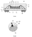
- FIG. 1A is a cross-sectional view illustrating a semiconductor device according to an embodiment of the present invention.
- FIG. 1B is an enlarged view illustrating area 1 B of FIG. 1A ;
- FIG. 1C is a plan view of a semiconductor die used in the semiconductor device according to the embodiment of the present invention.
- FIG. 2A is a cross-sectional view illustrating a semiconductor device according to a further embodiment of the present invention.
- FIG. 2B is an enlarged view illustrating area 2 B of FIG. 2A ;
- FIG. 3A is a cross-sectional view illustrating a semiconductor device according to another embodiment of the present invention.
- FIG. 3B is an enlarged view illustrating area 3 B of FIG. 3A ;
- FIG. 4 is a cross-sectional view illustrating a semiconductor device according to another embodiment of the present invention.
- FIG. 5 is a flow chart for explaining a method for fabricating a semiconductor device according to an embodiment of the present invention.
- FIGS. 6A , 6 B, 6 C, 6 D, 6 E, 6 F are cross-sectional views for explaining a method for fabricating a semiconductor device according to an embodiment of the present invention.
- FIG. 1A there is illustrated a cross-sectional view of a semiconductor device 100 according to an embodiment of the present invention.
- FIG. 1B there is illustrated an enlarged view of area 1 B of FIG. 1A .
- FIG. 1C there is illustrated a plan view of a semiconductor die 130 used in the semiconductor device 100 according to the embodiment of the present invention.
- the semiconductor die 100 comprises a substrate 110 , a semiconductor die 130 attached to the upper surface of the substrate 110 , conductive wires 140 electrically connecting the substrate 110 to the semiconductor die 130 , and an encapsulant 150 formed surrounding the semiconductor die 130 .
- the semiconductor device 100 may further comprise solder balls 160 formed under the substrate 110 .
- the substrate 110 provides a base for the fabrication of the semiconductor device 110 .
- the substrate 110 includes an insulating layer 111 , lands 112 formed on the lower surface of the insulating layer 111 , conductive vias 113 penetrating the insulating layer 111 and connected to the respective lands 112 , conductive patterns 114 formed on the upper surface of the insulating layer 111 to be connected to the respective conductive vias 113 , and a solder mask 115 covering an area other than areas where the lands 112 are formed.
- the insulating layer 111 is substantially in the form of a thin plate and plays a basic role in insulating the overlying semiconductor die 130 from an external circuit. To this end, the insulating layer 111 is formed of an electrically insulating material such as a thermosetting resin or a polymer (e.g., polyimide).
- an electrically insulating material such as a thermosetting resin or a polymer (e.g., polyimide).
- the lands 112 are formed on the lower surface of the insulating layer 111 . Only one land 112 may be provided. In the case of a land grid array (LGA) type, the lands 112 are directly electrically connected to an external circuit. In the case of a ball grid array (BGA) type, the lands 112 are electrically connected to an external circuit through solder balls 160 . To this end, the lands 112 are made of highly electrically conductive copper or its equivalent.
- LGA land grid array
- BGA ball grid array
- the conductive vias 113 are formed so as to penetrate the insulating layer 111 in relation to the respective lands 112 .
- the conductive vias 113 electrically connect the lands 112 and the respective conductive patterns 114 .
- the conductive vias 113 may be formed by filling via-holes with a metal when the conductive patterns 114 are formed.
- the conductive vias 113 are made of highly electrically conductive copper or its equivalent.
- the conductive patterns 114 are formed on the upper surface of the insulating layer 111 .
- the conductive patterns 114 are electrically connected to the semiconductor die 130 .
- the conductive patterns 114 are electrically connected to an external circuit through the conductive vias 113 and the lands 112 .
- the conductive patterns 114 are made of highly electrically conductive copper or its equivalent.
- the solder mask 115 is formed on the lower surface of the insulating layer 111 .
- the solder mask 115 is formed so as to cover an area other than areas where the lands 112 are exposed.
- the solder mask 115 is formed of a highly insulating material selected from benzocyclobutene (BCB) resins, polyimide and equivalents thereof.
- the semiconductor die 130 is attached to the upper surface of the substrate 110 by means of an adhesive 120 .
- the adhesive is a highly viscous material (such as an epoxy resin or an adhesive tape) or its equivalent.
- the semiconductor die 130 is an integrated circuit made of single-crystal silicon, polycrystalline silicon, amorphous silicon or an equivalent thereof as a main material using a semiconductor manufacturing process.
- the semiconductor die 130 includes one or more bond pads 131 ( 131 a ; 131 b ) on the upper surface thereof.
- the bond pads 131 provide passages through which the semiconductor die 130 electrically inputs/outputs signals from/to the outside.
- Each of the bond pads 131 is divided into the first bond pad 131 a and the second bond pad 131 b .
- First bond pad 131 a is sometimes called a protected or cathodic bond pad 131 a .
- Second bond pad 131 b is sometimes called a sacrificial or anodic bond pad 131 b .
- the first bond pads 131 a contact and are electrically connected to the respective second bond pads 131 b.
- the first bond pad 131 a is positioned outwardly relative to the second bond pad 131 b in the region of the bond pad 131 .
- the first bond pad 131 a is bonded to the corresponding conductive wire 140 and is connected to the corresponding conductive pattern 114 of the substrate 110 through the conductive wire 140 . Accordingly, the outward positioning of the first bond pads 131 a with respect to a plane parallel to the upper surface of the semiconductor die 130 , sometimes called the plane of the semiconductor die 130 , leads to a reduction in the length of the conductive wires 140 , thus contributing to the reduction of electrical noise signals.
- the first bond pads 131 a can be made of aluminum.
- Each of the second bond pads 131 b is positioned more inwardly than and in lateral contact with the corresponding first bond pad 131 a .
- the second bond pads 131 b prevent the occurrence of galvanic corrosion in the first bond pads 131 a .
- the second bond pads 131 b are made of a metal having a higher ionization tendency than a metal for the first bond pads 131 a , so that the second bond pads 131 b can be more readily oxidized than the first bond pads 131 a . That is, the second bond pads 131 b function as sacrificial anodes and are corroded at a higher rate than the first bond pads 131 a .
- the second bond pads are made of a material selected from magnesium, magnesium alloys, zinc, zinc alloys, cadmium, beryllium, and combinations thereof.
- the oxidation/corrosion mechanism of the bond pads 131 prevents the occurrence of galvanic corrosion at the interfaces between the first bond pads 131 a and the conductive wires 140 after bonding.
- the second bond pads 131 b may be marked instead of the first bond pads 131 b , which ensures firm bonding between the conductive wires 140 and the first bond pads 131 a.
- the bond pads 131 include the first bond pads 131 a and at least one second bond pad 131 b electrically connected to the first bond pads 131 a . In this case, there is no restriction on the position of the second bond pads 131 b on the upper surface of the semiconductor die 130 .
- This irregular configuration of the bond pads 131 is disadvantageous in terms of anticorrosive effects but allows the formation of the second bond pads 131 b in a simple manner, which enables the fabrication of the semiconductor device 100 at reduced cost, when compared to the configuration of the first and second bond pads 131 a and 131 b in a one-to-one relationship.
- the conductive wires 140 electrically connect the substrate 110 and the semiconductor die 130 . Specifically, the conductive wires 140 electrically connect the conductive patterns 114 of the substrate 110 and the first bond pads 131 a of the semiconductor die 130 .
- the conductive wires 140 may be made of a highly conductive material, such as gold, silver or copper.
- the use of the second bond pads 131 b made of a material having a higher ionization tendency than a material for the first bond pads 131 a in the semiconductor device 100 according to the embodiment of the present invention prevents the occurrence of galvanic corrosion in the bond pads 131 of the semiconductor die 130 .
- the encapsulant 150 is formed surrounding the semiconductor die 130 and the conductive wires 140 on the substrate 110 .
- the encapsulant 150 protects the elements from the ambient environment.
- the encapsulant 150 is formed using a material selected from epoxy resins, silicone resins and equivalents thereof that are widely used in the art.
- the solder balls 160 have a substantially spherical shape and are connected to the lower surface of the substrate 110 .
- the solder balls 160 electrically connect the lands 112 of the substrate 110 and an external circuit.
- the solder balls 160 are easy to produce and handle and are made of a material selected from tin, lead, silver, silver alloys and combinations thereof, all of which have melting points.
- each of the bond pads 131 of the semiconductor die 130 consists of the first bond pad 131 a made of a material whose ionization tendency is relatively low and the second bond pad 131 b made of a material whose ionization tendency is relatively high. Therefore, the second bond pads 131 b function as sacrificial anodes to prevent the occurrence of galvanic corrosion in the first bond pads 131 a bonded to the conductive wires 140 and to prevent damage of the first bond pads 131 a resulting from marking by a probe.
- FIG. 2A there is illustrated a cross-sectional view of the semiconductor device 200 .
- FIG. 2B there is illustrated an enlarged view of area 2 B of FIG. 2A .
- the semiconductor device 200 comprises a substrate 110 , a semiconductor die 230 attached to the substrate 110 by means of an adhesive 120 , conductive wires 140 , and an encapsulant 150 .
- the semiconductor device 200 may further comprise solder balls 160 formed under the substrate 110 .
- the same reference numerals are used to designate elements having the same structure and function as the elements of the previous embodiment. Differences of the semiconductor device 200 from the semiconductor device 100 will be mainly explained below.
- the semiconductor die 230 is attached to the upper surface of the substrate 110 by means of the adhesive 120 .
- the semiconductor die 230 includes one or more bond pads 231 ( 231 a ; 231 b ) on the upper surface thereof.
- each bond pad 231 includes a first bond pad 231 a and a second bond pad 231 b .
- First bond pad 231 a is sometimes called a protected or cathodic bond pad 231 a .
- Second bond pad 231 b is sometimes called a sacrificial or anodic bond pad 231 b.
- the first bond pads 231 a are formed on the upper surface of the semiconductor die 230 and are inwardly indented to a predetermined depth to form the second bond pads 231 b.
- the bond pads 231 are planar in shape, which is determined as a whole by the shape of the first bond pads 231 a . Inner portions of the first bond pads 231 a with respect to the plane of the semiconductor die 230 are etched to a predetermined depth to form etched cavities, sometimes called etched portions, in the first bond pads 231 a .
- the second bond pads 231 b are formed in the respective etched cavities of the first bond pads 231 a .
- the first bond pads 231 a are connected to conductive patterns 114 of the substrate 110 through the respective conductive wires 140 .
- the second bond pads 231 b are filled in the etched portions of the first bond pads 231 a .
- the second bond pads 231 b are made of a material whose ionization tendency is higher than a material for the first bond pads 231 a . Accordingly, the second bond pads 231 b function as sacrificial anodes to prevent the first bond pads 231 a from galvanic corrosion.
- the bond pads 231 are formed by etching inner portions of the first bond pads 231 a with respect to the plane of the semiconductor die 230 to a predetermined depth and forming the second bond pads 231 b in the respective etched portions of the first bond pads 231 a to prevent the first bond pads 231 a from galvanic corrosion.
- FIG. 3A there is illustrated a cross-sectional view of the semiconductor device 300 .
- FIG. 3B there is illustrated an enlarged view of area 3 B of FIG. 3A .
- the semiconductor device 300 comprises a substrate 110 , a semiconductor die 330 attached to the substrate 110 by means of an adhesive 120 , conductive wires 140 , and an encapsulant 150 .
- the semiconductor device 300 may further comprise solder balls 160 formed under the substrate 110 .
- the same reference numerals are used to designate elements having the same structure and function as the elements of the previous embodiments. Differences of the semiconductor device 300 and the semiconductor devices 100 and 200 will be mainly explained below.
- the semiconductor die 330 is attached to the upper surface of the substrate 110 by means the adhesive 120 .
- the semiconductor die 330 includes one or more bond pads 331 ( 331 a ; 331 b ) on the upper surface thereof.
- each bond pad 331 includes a first bond pad 331 a and a second bond pad 331 b .
- First bond pad 331 a is sometimes called a protected or cathodic bond pad 331 a .
- Second bond pad 331 b is sometimes called a sacrificial or anodic bond pad 331 b.
- the first bond pads 331 a are formed on the upper surface of the semiconductor die 330 .
- the bond pads 331 are substantially planar in shape, which is determined as a whole by the shape of the first bond pads 331 a .
- a portion of the upper surface of each of the first bond pads 331 a is covered with the corresponding second bond pad 331 b .
- the first bond pads 331 a are connected to conductive patterns 114 of the substrate 110 through the respective conductive wires 140 .
- Each of the second bond pads 331 b is formed on a portion of the upper surface of the first bond pad 331 a .
- the second bond pad 331 b protrudes from the inner portion of the first bond pad 331 a with respect to the plane of the semiconductor die 330 .
- the second bond pads 331 b are made of a material having a higher ionization tendency than a material for the first bond pads 331 a to prevent the first bond pads 331 a from galvanic corrosion. Further, the second bond pads 331 b are formed in an easy manner on the upper surfaces of the first bond pads 331 a without the need for additional etching, which enables the fabrication of the semiconductor device 300 at reduced cost.
- the first bond pads 331 a are made of a material whose ionization tendency is relatively low and the second bond pads 331 b are made of a material whose ionization tendency is relatively high. Therefore, the second bond pads 331 b can be formed by relatively simple processing to prevent the first bond pads 331 a bonded to the conductive wires 140 from galvanic corrosion.
- FIG. 4 there is illustrated a cross-sectional view of the semiconductor device 400 .
- the semiconductor device 400 comprises a substrate 110 , a semiconductor die 130 attached to the substrate 110 by means of an adhesive 120 , conductive wires 140 , a film-over-wire (FOW) 420 formed on the semiconductor die, another semiconductor die 430 stacked on the FOW 420 , conductive wires 440 connecting the semiconductor die 430 to the substrate 110 , and an encapsulant 150 .
- the semiconductor device 400 may further comprise solder balls 160 formed under the substrate 110 .
- the same reference numerals are used to designate elements having the same structure and function as the elements of the previous embodiments. Differences of the semiconductor device 400 from the semiconductor devices 100 , 200 and 300 will be mainly explained below.
- the FOW 420 is formed so as to surround wire loops of the conductive wires 140 connected to the semiconductor die 130 .
- the FOW 420 can be formed of a general epoxy resin.
- the FOW 420 has a uniform thickness and the semiconductor die 430 is stacked thereon.
- the FOW 420 may surround portions of the conductive wires 140 before being solidified.
- the FOW 420 may be attached to the lower surface of the semiconductor die 430 , bonded to upper portions of the conductive wires 140 , and solidified.
- the FOW 420 is solidified by heating. However, heating may increase the risk of galvanic corrosion at the interfaces between the first bond pads 131 a and the conductive wires 140 .
- This risk can be avoided by forming second bond pads 131 b in lateral contact with the first bond pads 131 a using a material having a higher ionization tendency than a material for the first bond pads 131 a to function as sacrificial anodes. Accordingly, corrosion occurs in the second bond pads 131 b rather than in the first bond pads 131 a . That is, the second bond pads 131 b prevent the occurrence of corrosion at the interfaces between the first bond pads 131 a and the conductive wires 140 , which makes the bonding between the first bond pads 131 a and the conductive wires 140 stronger.
- the semiconductor die 430 stacked on the FOW 420 has the same constitution as the semiconductor die 130 . That is, the semiconductor die 430 includes bond pads 431 ( 431 a ; 431 b ) corresponding to the bond pads 131 of the semiconductor die 130 . Each of the bond pads 431 is divided into the first bond pad 431 a and the second bond pad 431 b in lateral contact with the first bond pad 431 a .
- the semiconductor die 430 may be provided in plurality. In this case, a plurality of FOWs may also be used to stack the semiconductor dies 430 .
- the semiconductor die 130 and the semiconductor die 430 exemplify the semiconductor die 130 of the semiconductor device 100 according to the previous embodiment of the present invention. However, it should be understood that the semiconductor die 130 and the semiconductor die 430 can be independently selected from the semiconductor dies 130 , 230 and 330 of the semiconductor devices 100 , 200 and 300 according to the previous embodiments of the present invention.
- the conductive wires 440 electrically connect lands 114 of the substrate 110 and the first bond pads 431 a of the semiconductor die 430 .
- the conductive wires 440 have the same constitution as the conductive wires 140 .
- At least one semiconductor die 430 can be stacked on the FOW 420 overlying the semiconductor die 130 , and the semiconductor die 130 includes the first bond pads 131 a and the second bond pads 131 b .
- This construction can prevent the occurrence of corrosion at the interfaces between the first bond pads 131 a and the conductive wires 140 during heating for the solidification of the FOW 420 .
- the semiconductor device having a lead frame structure.
- the semiconductor device comprises a lead frame having lands exposed to the lower surface thereof and/or leads exposed to the side surfaces thereof as a substrate, a semiconductor die attached to the upper surface of the substrate and having bond pads on the upper surface thereof, and conductive wires connecting the lands and/or the leads of the substrate to the bond pads of the semiconductor die.
- Each of the bond pads of the semiconductor die consists of a first bond pad made of a material whose ionization tendency is relatively low and a second bond pad made of a material whose ionization tendency is relatively high. Therefore, the second bond pads function as sacrificial anodes to prevent the occurrence of galvanic corrosion in the first bond pads bonded to the conductive wires.
- FIG. 5 there is illustrated a flow chart for explaining the method according to the embodiment of the present invention.
- FIGS. 6A through 6F there are illustrated cross-sectional views for explaining the method according to the embodiment of the present invention.
- the method comprises the following operations: a formation of pad regions operation S 1 , a die attachment operation S 2 , a wire bonding operation S 3 and an encapsulation operation S 4 .
- the method may further comprise the operation of a formation of solder balls operation S 5 after encapsulation operation S 4 .
- the individual operations of the method illustrated in FIG. 5 will be explained with reference to FIGS. 6A through 6F .
- bond pads 131 are formed on a semiconductor die 130 in formation of pad regions operation S 1 .
- the first bond pads 131 a are formed on the semiconductor die 130
- the second bond pads 131 b are formed so as to be in lateral contact with the respective first bond pads 131 a .
- the second bond pads 131 b are positioned more inwardly than the first bond pads 131 a with respect to the plane of the semiconductor die 130 .
- the second bond pads 131 b can be formed by forming a pattern using a photoresist, plating a metal on the pattern by electroplating or electroless plating, and removing the photoresist.
- the metal can be selected from magnesium, magnesium alloys, zinc, zinc alloys, cadmium, beryllium and combinations thereof.
- the semiconductor die 130 is attached to the upper surface of a substrate 110 by means of an adhesive 120 in die attachment operation S 2 .
- the adhesive 120 include, but are not limited to, epoxy resins, adhesive tapes and equivalents thereof.
- the substrate 110 is electrically connected to the semiconductor die 130 through conductive wires 140 in wire bonding operation S 3 .
- the conductive wires 140 electrically connect conductive patterns 114 of the substrate 110 and the first bond pads 131 a of the semiconductor die 130 .
- the conductive wires 140 can be made of a material selected from gold, silver, copper and combinations thereof.
- the second bond pads 131 b prevent the occurrence of galvanic corrosion at the interfaces between the conductive wires 140 and the first bond pads 131 a.
- Suitable materials for the encapsulant 150 include epoxy resins, silicone resins and equivalents thereof, but are not limited thereto.
- the method may further comprise the operation of forming solder balls 160 on the lower surface of the substrate 110 in solder balls operation S 5 , as illustrated in FIG. 5 and FIG. 6F .
- the solder balls 160 are electrically connected to lands 112 of the substrate 110 .
- the solder balls 160 can be made of a material selected from tin, lead, silver, silver alloys and combinations thereof.
- the second bond pads 131 b prevent the occurrence of galvanic corrosion at the interfaces between the first bond pads 131 a and the conductive wires 140 .
- formation of pad regions operation S 1 may be carried out by forming first bond pads 231 a , etching portions of the first bond pads 231 a , and electroplating or electroless plating a metal on the etched portions to form second bond pads 231 b.
- formation of pad regions operation S 1 may be carried out by forming first bond pads 331 a and electroplating or electroless plating a metal on the inner upper surfaces of the first bond pads 331 a to form second bond pads 331 b.
- the subsequent operations are the same as those of the method for fabricating the semiconductor device 100 .
- a series of operations of forming a FOW 420 , attaching a semiconductor die 430 to the FOW 420 and connecting the substrate 110 to the semiconductor die 430 through conductive wires 440 is repeated at least one time between wire bonding operation S 3 and encapsulation operation S 4 .
- the semiconductor device having a lead frame structure can be fabricated by preparing a lead frame as the substrate and carrying out operations S 1 through S 4 .
Abstract
Description
Claims (18)
Priority Applications (1)
| Application Number | Priority Date | Filing Date | Title |
|---|---|---|---|
| US12/549,068 US8183683B1 (en) | 2009-08-27 | 2009-08-27 | Semiconductor device and fabricating method thereof |
Applications Claiming Priority (1)
| Application Number | Priority Date | Filing Date | Title |
|---|---|---|---|
| US12/549,068 US8183683B1 (en) | 2009-08-27 | 2009-08-27 | Semiconductor device and fabricating method thereof |
Publications (1)
| Publication Number | Publication Date |
|---|---|
| US8183683B1 true US8183683B1 (en) | 2012-05-22 |
Family
ID=46061255
Family Applications (1)
| Application Number | Title | Priority Date | Filing Date |
|---|---|---|---|
| US12/549,068 Active 2030-07-29 US8183683B1 (en) | 2009-08-27 | 2009-08-27 | Semiconductor device and fabricating method thereof |
Country Status (1)
| Country | Link |
|---|---|
| US (1) | US8183683B1 (en) |
Cited By (4)
| Publication number | Priority date | Publication date | Assignee | Title |
|---|---|---|---|---|
| US20140367684A1 (en) * | 2013-06-12 | 2014-12-18 | International Business Machines Corporation | Methods for testing integrated circuits of wafer and testing structures for integrated circuits |
| US9412709B2 (en) | 2013-05-21 | 2016-08-09 | Freescale Semiconductor, Inc. | Semiconductor structure with sacrificial anode and passivation layer and method for forming |
| CN106057762A (en) * | 2015-04-17 | 2016-10-26 | 半导体元件工业有限责任公司 | Wire bonding systems and related methods |
| US9608403B2 (en) | 2014-11-03 | 2017-03-28 | International Business Machines Corporation | Dual bond pad structure for photonics |
Citations (4)
| Publication number | Priority date | Publication date | Assignee | Title |
|---|---|---|---|---|
| US6306751B1 (en) * | 1999-09-27 | 2001-10-23 | Lsi Logic Corporation | Apparatus and method for improving ball joints in semiconductor packages |
| US6348742B1 (en) * | 1999-01-25 | 2002-02-19 | Clear Logic, Inc. | Sacrificial bond pads for laser configured integrated circuits |
| US6515366B1 (en) * | 2002-02-14 | 2003-02-04 | Taiwan Semiconductor Manufacturing Company, Ltd. | Reduction of metal corrosion in semiconductor devices |
| US6849533B2 (en) * | 2003-01-29 | 2005-02-01 | Taiwan Semiconductor Manufacturing Co., Ltd | Method for fabricating microelectronic product with attenuated bond pad corrosion |
-
2009
- 2009-08-27 US US12/549,068 patent/US8183683B1/en active Active
Patent Citations (4)
| Publication number | Priority date | Publication date | Assignee | Title |
|---|---|---|---|---|
| US6348742B1 (en) * | 1999-01-25 | 2002-02-19 | Clear Logic, Inc. | Sacrificial bond pads for laser configured integrated circuits |
| US6306751B1 (en) * | 1999-09-27 | 2001-10-23 | Lsi Logic Corporation | Apparatus and method for improving ball joints in semiconductor packages |
| US6515366B1 (en) * | 2002-02-14 | 2003-02-04 | Taiwan Semiconductor Manufacturing Company, Ltd. | Reduction of metal corrosion in semiconductor devices |
| US6849533B2 (en) * | 2003-01-29 | 2005-02-01 | Taiwan Semiconductor Manufacturing Co., Ltd | Method for fabricating microelectronic product with attenuated bond pad corrosion |
Cited By (12)
| Publication number | Priority date | Publication date | Assignee | Title |
|---|---|---|---|---|
| US9412709B2 (en) | 2013-05-21 | 2016-08-09 | Freescale Semiconductor, Inc. | Semiconductor structure with sacrificial anode and passivation layer and method for forming |
| US10199339B2 (en) | 2013-05-21 | 2019-02-05 | Nxp Usa, Inc. | Semiconductor structure with sacrificial anode and method for forming |
| US20140367684A1 (en) * | 2013-06-12 | 2014-12-18 | International Business Machines Corporation | Methods for testing integrated circuits of wafer and testing structures for integrated circuits |
| US9269642B2 (en) * | 2013-06-12 | 2016-02-23 | Globalfoundries Inc. | Methods for testing integrated circuits of wafer and testing structures for integrated circuits |
| US9608403B2 (en) | 2014-11-03 | 2017-03-28 | International Business Machines Corporation | Dual bond pad structure for photonics |
| US10476227B2 (en) | 2014-11-03 | 2019-11-12 | International Business Machines Corporation | Dual bond pad structure for photonics |
| US10833038B2 (en) | 2014-11-03 | 2020-11-10 | International Business Machines Corporation | Dual bond pad structure for photonics |
| US10978416B2 (en) | 2014-11-03 | 2021-04-13 | International Business Machines Corporation | Dual bond pad structure for photonics |
| CN106057762A (en) * | 2015-04-17 | 2016-10-26 | 半导体元件工业有限责任公司 | Wire bonding systems and related methods |
| US20190013290A1 (en) * | 2015-04-17 | 2019-01-10 | Semiconductor Components Industries, Llc | Wire bonding systems and related methods |
| US10535623B2 (en) * | 2015-04-17 | 2020-01-14 | Semiconductor Components Industries, Llc | Wire bonding systems and related methods |
| CN106057762B (en) * | 2015-04-17 | 2021-03-16 | 半导体元件工业有限责任公司 | Wire bonding system and related method |
Similar Documents
| Publication | Publication Date | Title |
|---|---|---|
| KR100671921B1 (en) | Semiconductor device and manufacturing method thereof | |
| KR100563887B1 (en) | Semiconductor device and manufacturing method thereof | |
| JP4850392B2 (en) | Manufacturing method of semiconductor device | |
| US9595453B2 (en) | Chip package method and package assembly | |
| KR100709662B1 (en) | Semiconductor device and manufacturing method thereof | |
| US20100178734A1 (en) | Leadless Semiconductor Package with Electroplated Layer Embedded in Encapsulant and the Method for Manufacturing the Same | |
| US10229892B2 (en) | Semiconductor package and method for manufacturing a semiconductor package | |
| US9177837B2 (en) | Fabrication method of semiconductor package having electrical connecting structures | |
| TW201507080A (en) | Embedded packaging with preformed vias | |
| US20110163430A1 (en) | Leadframe Structure, Advanced Quad Flat No Lead Package Structure Using the Same, and Manufacturing Methods Thereof | |
| US20110159643A1 (en) | Fabrication method of semiconductor package structure | |
| US8067698B2 (en) | Wiring substrate for use in semiconductor apparatus, method for fabricating the same, and semiconductor apparatus using the same | |
| KR20040101924A (en) | Semiconductor device and method for manufacturing the same | |
| KR100551576B1 (en) | Semiconductor device and method of producing the same | |
| US9704747B2 (en) | Semiconductor device and manufacturing method thereof | |
| KR20200068958A (en) | Connection structure and method of forming the same | |
| US8183683B1 (en) | Semiconductor device and fabricating method thereof | |
| US20170372988A1 (en) | Wafer level chip scale semiconductor package | |
| US9461009B1 (en) | Method and apparatus for assembling a semiconductor package | |
| JP2014078658A (en) | Substrate for semiconductor package and manufacturing method of the same | |
| US11348863B2 (en) | Semiconductor package having a semiconductor die on a plated conductive layer | |
| US20080006940A1 (en) | Lead frames, microelectronic devices with lead frames, and methods for manufacturing lead frames and microelectronic devices with lead frames | |
| JP4511148B2 (en) | Manufacturing method of semiconductor device | |
| JP2017191840A (en) | Semiconductor device and method of manufacturing semiconductor device | |
| TWI816063B (en) | Semiconductor device and manufacturing method thereof |
Legal Events
| Date | Code | Title | Description |
|---|---|---|---|
| AS | Assignment |
Owner name: AMKOR TECHNOLOGY, INC., ARIZONA Free format text: ASSIGNMENT OF ASSIGNORS INTEREST;ASSIGNORS:KIM, JOON SU;PARK, JUNG SOO;HWANG, TAE KYUNG;SIGNING DATES FROM 20090819 TO 20090821;REEL/FRAME:023158/0330 |
|
| STCF | Information on status: patent grant |
Free format text: PATENTED CASE |
|
| AS | Assignment |
Owner name: BANK OF AMERICA, N.A., TEXAS Free format text: PATENT SECURITY AGREEMENT;ASSIGNOR:AMKOR TECHNOLOGY, INC.;REEL/FRAME:029422/0178 Effective date: 20120913 |
|
| FPAY | Fee payment |
Year of fee payment: 4 |
|
| AS | Assignment |
Owner name: BANK OF AMERICA, N.A., AS AGENT, CALIFORNIA Free format text: SECURITY INTEREST;ASSIGNOR:AMKOR TECHNOLOGY, INC.;REEL/FRAME:046683/0139 Effective date: 20180713 |
|
| MAFP | Maintenance fee payment |
Free format text: PAYMENT OF MAINTENANCE FEE, 8TH YEAR, LARGE ENTITY (ORIGINAL EVENT CODE: M1552); ENTITY STATUS OF PATENT OWNER: LARGE ENTITY Year of fee payment: 8 |
|
| AS | Assignment |
Owner name: AMKOR TECHNOLOGY SINGAPORE HOLDING PTE.LTD., SINGAPORE Free format text: ASSIGNMENT OF ASSIGNORS INTEREST;ASSIGNOR:AMKOR TECHNOLOGY, INC.;REEL/FRAME:054067/0135 Effective date: 20191119 |
|
| MAFP | Maintenance fee payment |
Free format text: PAYMENT OF MAINTENANCE FEE, 12TH YEAR, LARGE ENTITY (ORIGINAL EVENT CODE: M1553); ENTITY STATUS OF PATENT OWNER: LARGE ENTITY Year of fee payment: 12 |