EP3528299B1 - Manufacturing method of a transparent oled display - Google Patents
Manufacturing method of a transparent oled display Download PDFInfo
- Publication number
- EP3528299B1 EP3528299B1 EP16918595.6A EP16918595A EP3528299B1 EP 3528299 B1 EP3528299 B1 EP 3528299B1 EP 16918595 A EP16918595 A EP 16918595A EP 3528299 B1 EP3528299 B1 EP 3528299B1
- Authority
- EP
- European Patent Office
- Prior art keywords
- manufacturing
- transparent
- cathode
- etl
- htl
- Prior art date
- Legal status (The legal status is an assumption and is not a legal conclusion. Google has not performed a legal analysis and makes no representation as to the accuracy of the status listed.)
- Active
Links
- 238000004519 manufacturing process Methods 0.000 title claims description 46
- 239000000758 substrate Substances 0.000 claims description 65
- 238000000034 method Methods 0.000 claims description 41
- 150000003254 radicals Chemical class 0.000 claims description 37
- 239000000463 material Substances 0.000 claims description 36
- 230000008569 process Effects 0.000 claims description 32
- 238000004528 spin coating Methods 0.000 claims description 15
- 239000011368 organic material Substances 0.000 claims description 14
- 229910044991 metal oxide Inorganic materials 0.000 claims description 11
- 150000004706 metal oxides Chemical class 0.000 claims description 11
- XLOMVQKBTHCTTD-UHFFFAOYSA-N Zinc monoxide Chemical compound [Zn]=O XLOMVQKBTHCTTD-UHFFFAOYSA-N 0.000 claims description 10
- 238000005507 spraying Methods 0.000 claims description 10
- 230000005525 hole transport Effects 0.000 claims description 8
- 238000006243 chemical reaction Methods 0.000 claims description 7
- -1 N, N-dimethylaminopropyl Chemical group 0.000 claims description 6
- RMBPEFMHABBEKP-UHFFFAOYSA-N fluorene Chemical compound C1=CC=C2C3=C[CH]C=CC3=CC2=C1 RMBPEFMHABBEKP-UHFFFAOYSA-N 0.000 claims description 6
- NIHNNTQXNPWCJQ-UHFFFAOYSA-N o-biphenylenemethane Natural products C1=CC=C2CC3=CC=CC=C3C2=C1 NIHNNTQXNPWCJQ-UHFFFAOYSA-N 0.000 claims description 6
- 239000010409 thin film Substances 0.000 claims description 6
- 230000008020 evaporation Effects 0.000 claims description 5
- 238000001704 evaporation Methods 0.000 claims description 5
- 239000011787 zinc oxide Substances 0.000 claims description 4
- 238000010030 laminating Methods 0.000 claims description 3
- 239000004065 semiconductor Substances 0.000 description 7
- 230000008901 benefit Effects 0.000 description 5
- 238000005516 engineering process Methods 0.000 description 5
- 239000000243 solution Substances 0.000 description 5
- 238000004544 sputter deposition Methods 0.000 description 5
- OKTJSMMVPCPJKN-UHFFFAOYSA-N Carbon Chemical compound [C] OKTJSMMVPCPJKN-UHFFFAOYSA-N 0.000 description 4
- 150000001875 compounds Chemical class 0.000 description 4
- 230000006378 damage Effects 0.000 description 4
- 239000010408 film Substances 0.000 description 4
- 229910002804 graphite Inorganic materials 0.000 description 4
- 239000010439 graphite Substances 0.000 description 4
- 229920001621 AMOLED Polymers 0.000 description 3
- 239000002131 composite material Substances 0.000 description 3
- 239000007772 electrode material Substances 0.000 description 3
- 238000010438 heat treatment Methods 0.000 description 3
- 239000012528 membrane Substances 0.000 description 3
- GFLJTEHFZZNCTR-UHFFFAOYSA-N 3-prop-2-enoyloxypropyl prop-2-enoate Chemical compound C=CC(=O)OCCCOC(=O)C=C GFLJTEHFZZNCTR-UHFFFAOYSA-N 0.000 description 2
- 239000011521 glass Substances 0.000 description 2
- AMGQUBHHOARCQH-UHFFFAOYSA-N indium;oxotin Chemical compound [In].[Sn]=O AMGQUBHHOARCQH-UHFFFAOYSA-N 0.000 description 2
- 239000011159 matrix material Substances 0.000 description 2
- 229920000371 poly(diallyldimethylammonium chloride) polymer Polymers 0.000 description 2
- 241000237519 Bivalvia Species 0.000 description 1
- 229910052782 aluminium Inorganic materials 0.000 description 1
- XAGFODPZIPBFFR-UHFFFAOYSA-N aluminium Chemical compound [Al] XAGFODPZIPBFFR-UHFFFAOYSA-N 0.000 description 1
- 230000004888 barrier function Effects 0.000 description 1
- 235000020639 clam Nutrition 0.000 description 1
- 238000004132 cross linking Methods 0.000 description 1
- 230000005684 electric field Effects 0.000 description 1
- 238000005286 illumination Methods 0.000 description 1
- 238000002347 injection Methods 0.000 description 1
- 239000007924 injection Substances 0.000 description 1
- 229910052751 metal Inorganic materials 0.000 description 1
- 239000002184 metal Substances 0.000 description 1
- 230000004048 modification Effects 0.000 description 1
- 238000012986 modification Methods 0.000 description 1
- 230000005693 optoelectronics Effects 0.000 description 1
- 238000004806 packaging method and process Methods 0.000 description 1
- 230000035515 penetration Effects 0.000 description 1
- 239000002243 precursor Substances 0.000 description 1
- 238000003825 pressing Methods 0.000 description 1
- 230000005855 radiation Effects 0.000 description 1
- 230000004044 response Effects 0.000 description 1
- 238000002791 soaking Methods 0.000 description 1
- 239000000126 substance Substances 0.000 description 1
- XLYOFNOQVPJJNP-UHFFFAOYSA-N water Substances O XLYOFNOQVPJJNP-UHFFFAOYSA-N 0.000 description 1
Images
Classifications
-
- H—ELECTRICITY
- H10—SEMICONDUCTOR DEVICES; ELECTRIC SOLID-STATE DEVICES NOT OTHERWISE PROVIDED FOR
- H10K—ORGANIC ELECTRIC SOLID-STATE DEVICES
- H10K71/00—Manufacture or treatment specially adapted for the organic devices covered by this subclass
-
- H—ELECTRICITY
- H10—SEMICONDUCTOR DEVICES; ELECTRIC SOLID-STATE DEVICES NOT OTHERWISE PROVIDED FOR
- H10K—ORGANIC ELECTRIC SOLID-STATE DEVICES
- H10K50/00—Organic light-emitting devices
-
- H—ELECTRICITY
- H10—SEMICONDUCTOR DEVICES; ELECTRIC SOLID-STATE DEVICES NOT OTHERWISE PROVIDED FOR
- H10K—ORGANIC ELECTRIC SOLID-STATE DEVICES
- H10K50/00—Organic light-emitting devices
- H10K50/10—OLEDs or polymer light-emitting diodes [PLED]
- H10K50/11—OLEDs or polymer light-emitting diodes [PLED] characterised by the electroluminescent [EL] layers
-
- H—ELECTRICITY
- H10—SEMICONDUCTOR DEVICES; ELECTRIC SOLID-STATE DEVICES NOT OTHERWISE PROVIDED FOR
- H10K—ORGANIC ELECTRIC SOLID-STATE DEVICES
- H10K50/00—Organic light-emitting devices
- H10K50/10—OLEDs or polymer light-emitting diodes [PLED]
- H10K50/14—Carrier transporting layers
- H10K50/15—Hole transporting layers
-
- H—ELECTRICITY
- H10—SEMICONDUCTOR DEVICES; ELECTRIC SOLID-STATE DEVICES NOT OTHERWISE PROVIDED FOR
- H10K—ORGANIC ELECTRIC SOLID-STATE DEVICES
- H10K50/00—Organic light-emitting devices
- H10K50/10—OLEDs or polymer light-emitting diodes [PLED]
- H10K50/14—Carrier transporting layers
- H10K50/16—Electron transporting layers
-
- H—ELECTRICITY
- H10—SEMICONDUCTOR DEVICES; ELECTRIC SOLID-STATE DEVICES NOT OTHERWISE PROVIDED FOR
- H10K—ORGANIC ELECTRIC SOLID-STATE DEVICES
- H10K50/00—Organic light-emitting devices
- H10K50/10—OLEDs or polymer light-emitting diodes [PLED]
- H10K50/17—Carrier injection layers
-
- H—ELECTRICITY
- H10—SEMICONDUCTOR DEVICES; ELECTRIC SOLID-STATE DEVICES NOT OTHERWISE PROVIDED FOR
- H10K—ORGANIC ELECTRIC SOLID-STATE DEVICES
- H10K50/00—Organic light-emitting devices
- H10K50/80—Constructional details
- H10K50/805—Electrodes
- H10K50/81—Anodes
-
- H—ELECTRICITY
- H10—SEMICONDUCTOR DEVICES; ELECTRIC SOLID-STATE DEVICES NOT OTHERWISE PROVIDED FOR
- H10K—ORGANIC ELECTRIC SOLID-STATE DEVICES
- H10K50/00—Organic light-emitting devices
- H10K50/80—Constructional details
- H10K50/805—Electrodes
- H10K50/82—Cathodes
-
- H—ELECTRICITY
- H10—SEMICONDUCTOR DEVICES; ELECTRIC SOLID-STATE DEVICES NOT OTHERWISE PROVIDED FOR
- H10K—ORGANIC ELECTRIC SOLID-STATE DEVICES
- H10K50/00—Organic light-emitting devices
- H10K50/80—Constructional details
- H10K50/805—Electrodes
- H10K50/82—Cathodes
- H10K50/828—Transparent cathodes, e.g. comprising thin metal layers
-
- H—ELECTRICITY
- H10—SEMICONDUCTOR DEVICES; ELECTRIC SOLID-STATE DEVICES NOT OTHERWISE PROVIDED FOR
- H10K—ORGANIC ELECTRIC SOLID-STATE DEVICES
- H10K50/00—Organic light-emitting devices
- H10K50/80—Constructional details
- H10K50/84—Passivation; Containers; Encapsulations
- H10K50/841—Self-supporting sealing arrangements
-
- H—ELECTRICITY
- H10—SEMICONDUCTOR DEVICES; ELECTRIC SOLID-STATE DEVICES NOT OTHERWISE PROVIDED FOR
- H10K—ORGANIC ELECTRIC SOLID-STATE DEVICES
- H10K59/00—Integrated devices, or assemblies of multiple devices, comprising at least one organic light-emitting element covered by group H10K50/00
- H10K59/10—OLED displays
- H10K59/12—Active-matrix OLED [AMOLED] displays
- H10K59/1201—Manufacture or treatment
-
- H—ELECTRICITY
- H10—SEMICONDUCTOR DEVICES; ELECTRIC SOLID-STATE DEVICES NOT OTHERWISE PROVIDED FOR
- H10K—ORGANIC ELECTRIC SOLID-STATE DEVICES
- H10K59/00—Integrated devices, or assemblies of multiple devices, comprising at least one organic light-emitting element covered by group H10K50/00
- H10K59/10—OLED displays
- H10K59/12—Active-matrix OLED [AMOLED] displays
- H10K59/123—Connection of the pixel electrodes to the thin film transistors [TFT]
-
- H—ELECTRICITY
- H10—SEMICONDUCTOR DEVICES; ELECTRIC SOLID-STATE DEVICES NOT OTHERWISE PROVIDED FOR
- H10K—ORGANIC ELECTRIC SOLID-STATE DEVICES
- H10K71/00—Manufacture or treatment specially adapted for the organic devices covered by this subclass
- H10K71/10—Deposition of organic active material
- H10K71/12—Deposition of organic active material using liquid deposition, e.g. spin coating
-
- H—ELECTRICITY
- H10—SEMICONDUCTOR DEVICES; ELECTRIC SOLID-STATE DEVICES NOT OTHERWISE PROVIDED FOR
- H10K—ORGANIC ELECTRIC SOLID-STATE DEVICES
- H10K71/00—Manufacture or treatment specially adapted for the organic devices covered by this subclass
- H10K71/10—Deposition of organic active material
- H10K71/16—Deposition of organic active material using physical vapour deposition [PVD], e.g. vacuum deposition or sputtering
- H10K71/164—Deposition of organic active material using physical vapour deposition [PVD], e.g. vacuum deposition or sputtering using vacuum deposition
-
- H—ELECTRICITY
- H10—SEMICONDUCTOR DEVICES; ELECTRIC SOLID-STATE DEVICES NOT OTHERWISE PROVIDED FOR
- H10K—ORGANIC ELECTRIC SOLID-STATE DEVICES
- H10K71/00—Manufacture or treatment specially adapted for the organic devices covered by this subclass
- H10K71/50—Forming devices by joining two substrates together, e.g. lamination techniques
-
- H—ELECTRICITY
- H10—SEMICONDUCTOR DEVICES; ELECTRIC SOLID-STATE DEVICES NOT OTHERWISE PROVIDED FOR
- H10K—ORGANIC ELECTRIC SOLID-STATE DEVICES
- H10K71/00—Manufacture or treatment specially adapted for the organic devices covered by this subclass
- H10K71/60—Forming conductive regions or layers, e.g. electrodes
-
- H—ELECTRICITY
- H10—SEMICONDUCTOR DEVICES; ELECTRIC SOLID-STATE DEVICES NOT OTHERWISE PROVIDED FOR
- H10K—ORGANIC ELECTRIC SOLID-STATE DEVICES
- H10K77/00—Constructional details of devices covered by this subclass and not covered by groups H10K10/80, H10K30/80, H10K50/80 or H10K59/80
- H10K77/10—Substrates, e.g. flexible substrates
- H10K77/111—Flexible substrates
-
- H—ELECTRICITY
- H10—SEMICONDUCTOR DEVICES; ELECTRIC SOLID-STATE DEVICES NOT OTHERWISE PROVIDED FOR
- H10K—ORGANIC ELECTRIC SOLID-STATE DEVICES
- H10K2102/00—Constructional details relating to the organic devices covered by this subclass
- H10K2102/10—Transparent electrodes, e.g. using graphene
- H10K2102/101—Transparent electrodes, e.g. using graphene comprising transparent conductive oxides [TCO]
- H10K2102/103—Transparent electrodes, e.g. using graphene comprising transparent conductive oxides [TCO] comprising indium oxides, e.g. ITO
-
- H—ELECTRICITY
- H10—SEMICONDUCTOR DEVICES; ELECTRIC SOLID-STATE DEVICES NOT OTHERWISE PROVIDED FOR
- H10K—ORGANIC ELECTRIC SOLID-STATE DEVICES
- H10K2102/00—Constructional details relating to the organic devices covered by this subclass
- H10K2102/301—Details of OLEDs
-
- H—ELECTRICITY
- H10—SEMICONDUCTOR DEVICES; ELECTRIC SOLID-STATE DEVICES NOT OTHERWISE PROVIDED FOR
- H10K—ORGANIC ELECTRIC SOLID-STATE DEVICES
- H10K2102/00—Constructional details relating to the organic devices covered by this subclass
- H10K2102/301—Details of OLEDs
- H10K2102/302—Details of OLEDs of OLED structures
- H10K2102/3023—Direction of light emission
- H10K2102/3031—Two-side emission, e.g. transparent OLEDs [TOLED]
-
- H—ELECTRICITY
- H10—SEMICONDUCTOR DEVICES; ELECTRIC SOLID-STATE DEVICES NOT OTHERWISE PROVIDED FOR
- H10K—ORGANIC ELECTRIC SOLID-STATE DEVICES
- H10K2102/00—Constructional details relating to the organic devices covered by this subclass
- H10K2102/301—Details of OLEDs
- H10K2102/311—Flexible OLED
-
- H—ELECTRICITY
- H10—SEMICONDUCTOR DEVICES; ELECTRIC SOLID-STATE DEVICES NOT OTHERWISE PROVIDED FOR
- H10K—ORGANIC ELECTRIC SOLID-STATE DEVICES
- H10K2102/00—Constructional details relating to the organic devices covered by this subclass
- H10K2102/301—Details of OLEDs
- H10K2102/321—Inverted OLED, i.e. having cathode between substrate and anode
-
- H—ELECTRICITY
- H10—SEMICONDUCTOR DEVICES; ELECTRIC SOLID-STATE DEVICES NOT OTHERWISE PROVIDED FOR
- H10K—ORGANIC ELECTRIC SOLID-STATE DEVICES
- H10K85/00—Organic materials used in the body or electrodes of devices covered by this subclass
- H10K85/10—Organic polymers or oligomers
- H10K85/111—Organic polymers or oligomers comprising aromatic, heteroaromatic, or aryl chains, e.g. polyaniline, polyphenylene or polyphenylene vinylene
- H10K85/115—Polyfluorene; Derivatives thereof
-
- H—ELECTRICITY
- H10—SEMICONDUCTOR DEVICES; ELECTRIC SOLID-STATE DEVICES NOT OTHERWISE PROVIDED FOR
- H10K—ORGANIC ELECTRIC SOLID-STATE DEVICES
- H10K85/00—Organic materials used in the body or electrodes of devices covered by this subclass
- H10K85/10—Organic polymers or oligomers
- H10K85/151—Copolymers
-
- Y—GENERAL TAGGING OF NEW TECHNOLOGICAL DEVELOPMENTS; GENERAL TAGGING OF CROSS-SECTIONAL TECHNOLOGIES SPANNING OVER SEVERAL SECTIONS OF THE IPC; TECHNICAL SUBJECTS COVERED BY FORMER USPC CROSS-REFERENCE ART COLLECTIONS [XRACs] AND DIGESTS
- Y02—TECHNOLOGIES OR APPLICATIONS FOR MITIGATION OR ADAPTATION AGAINST CLIMATE CHANGE
- Y02E—REDUCTION OF GREENHOUSE GAS [GHG] EMISSIONS, RELATED TO ENERGY GENERATION, TRANSMISSION OR DISTRIBUTION
- Y02E10/00—Energy generation through renewable energy sources
- Y02E10/50—Photovoltaic [PV] energy
- Y02E10/549—Organic PV cells
-
- Y—GENERAL TAGGING OF NEW TECHNOLOGICAL DEVELOPMENTS; GENERAL TAGGING OF CROSS-SECTIONAL TECHNOLOGIES SPANNING OVER SEVERAL SECTIONS OF THE IPC; TECHNICAL SUBJECTS COVERED BY FORMER USPC CROSS-REFERENCE ART COLLECTIONS [XRACs] AND DIGESTS
- Y02—TECHNOLOGIES OR APPLICATIONS FOR MITIGATION OR ADAPTATION AGAINST CLIMATE CHANGE
- Y02P—CLIMATE CHANGE MITIGATION TECHNOLOGIES IN THE PRODUCTION OR PROCESSING OF GOODS
- Y02P70/00—Climate change mitigation technologies in the production process for final industrial or consumer products
- Y02P70/50—Manufacturing or production processes characterised by the final manufactured product
Definitions
- the present invention relates to the field of display techniques, and in particular to a transparent OLED display and manufacturing method thereof.
- the organic light emitting diode (OLED) display also called organic electroluminescent display, is the new trend of flat panel display technology. Because the OLED display provides the advantages of simple manufacturing process, low cost, low power-consumption, high illumination, wide operating temperature range, thin size, short response time, enabling full-color large display, easy to match integrated circuit (IC) driver, and enabling flexible display, the OLED is recognized as the technology with widest application prospect.
- OLED organic light emitting diode
- the driving types of OLED can be divided according to the passive matrix OLED (PMOLED) and active matrix OLED (AMOLED), i.e., the direct addressable type and thin film transistor, TFT, addressable type, wherein the AMOLED provides the advantages of pixels arranged in an array, self-luminous, and high luminous efficiency and is commonly used for high definition large-size display.
- PMOLED passive matrix OLED
- AMOLED active matrix OLED
- TFT thin film transistor
- the structure of an OLED display comprises: a substrate, an anode disposed on the substrate, a hole inject layer, HIL, disposed on the anode, a hole transport layer (HTL) disposed on the HIL, a light-emitting layer disposed on the HTL, an electron transport layer, ETL, disposed on the light-emitting layer, an electron inject layer (EIL) disposed on the ETL, and a cathode disposed on the EIL.
- the light-emission principle of the OLED display is that the semiconductor material and the organic light-emitting material emit light through the carrier injection and compound driven by an electric field.
- the OLED display usually uses ITO pixel electrode and metal electrode respectively for the anode and cathode.
- the electrons and holes are injected into the ETL and HTL respectively from the cathode and anode.
- the electrons and the holes are migrated respectively to the light-emitting layer and encounter each other to form excitons and excite the light-emitting molecules, which emit visible lights through radiation relaxation.
- the transparent display technology is proposed due to the novelty display means.
- the transparent display device allows the viewer to see the images displayed by the display and the actual background behind the display.
- the transparent display has many possible applications, such as, window display for building or vehicles. Other than those large-area applications, the transparent display is also applicable to handheld devices, such as, viewing a map while also viewing the view behind the display.
- the majority of current display market is estimated to be replaced by the transparent displays, for example, in building, advertisements, and public information applications.
- the OLED Compared to TFT-LCD, the OLED provides the advantages of the ability to realize large-sized, ultra-thin, flexible and transparent displays.
- the manufacturing of transparent OLED display needs to solve the problem of transparent electrodes as the material for transparent electrodes must provide higher conductivity and high penetration rate.
- the main material for transparent electrode currently is ITO, which is often manufactured by sputtering process. The sputtering process may damage the organic light-emitting layer of the OLED when a too-high power is applied, and suffers a too-long film forming time and low yield rate when a too-low power is applied.
- US2005/009227A1 is a related prior art for this field. More particularly, US2005/009227A1 discloses a method to fabricate an organic electronic and opto-electronic device comprising: preparing a first part with at least a layer of a first organic material containing a first polymerisable group; preparing a second part with at least a layer of a second organic material containing a second polymerisable group; and bonding said first part to said second part under an environment with controlled parameters, wherein said bonding of said first part and said second part is achieved by cross-linking between said first polymerisable group and said second polymerisable groups.
- WO2006112537A1 is a related prior art for this field.
- JP 2013222750A is a related prior art for this field. More particularly, JP 2013222750A discloses a method for manufacturing a photoelectric conversion element capable of stably obtaining desired photoelectric conversion efficiency without damaging the structure of an electrode or an active layer and capable of being manufactured at low cost, wherein a first layer comprises an active layer and a first carrier transport layer which is an electron transport layer or a hole transport layer, or a precursor layer of the first carrier transport layer, on a first electrode.
- CN104966792A is a related prior art for this field. More particularly, CN104966792A discloses a composite film and a method for manufacturing the same, and an organic light-emitting diode and a method for packaging the same.
- the composite film comprises: a base membrane; a PDDA layer, which is deposited on a first surface of the base membrane; a graphite oxide layer, which is deposited on the PDDA layer; a monomolecular layer, which is self-assembled on a surface of the graphite oxide layer and is composed of a compound of Formula I.
- the method for manufacturing the composite film comprises a self-assembling step which includes placing and soaking a base membrane deposited with a graphite oxide layer in a solution of a compound of Formula I, and self-assembling the compound of Formula I on the graphite oxide layer.
- the object of the present invention is to provide a manufacturing method of transparent OLED display to improve yield rate and production efficiency.
- Another object of the present disclosure is to provide a transparent OLED display, which is easy to manufacture and provides high performance.
- the present invention provides a manufacturing method of transparent OLED display, which comprises: Step 1: providing a thin film transistor, TFT, array substrate, forming a cathode, an electron transport layer, ETL, a light-emitting layer and a hole transport layer (HTL) sequentially on the TFT array substrate to form a lower substrate, wherein the cathode being a transparent electrode, the HTL being made of an organic material with positive radicals; Step 2: providing an encapsulating cover plate, and forming an anode and a hole inject layer, HIL, on the encapsulating cover layer sequentially to form an upper substrate, wherein the anode being a transparent electrode, the HIL being made of an organic material with negative radicals; execution order of Step 1 and Step 2 being exchangeable; Step 3: laminating the upper substrate and the lower substrate in accordance with attaching the HTL and the HIL correspondingly, the positive radicals on the surface of the HTL and the negative radicals on the surface of the HIL being mutually
- Step 1 a spin coating process or a spraying process is used to form the ETL on the cathode; a spin coating process or an evaporation process is used to form the light-emitting layer on the ETL, and a spin coating process or a spraying process is used to form the HTL on the light-emitting layer.
- the materials of the cathode and the materials of the anode both comprise transparent conductive metal oxide.
- the materials of the ETL comprise at least one of zinc oxide and poly [9,9-dioctafluorene-9,9-bis (N, N-dimethylaminopropyl) fluorene].
- Step 3 is performed in a vacuum environment and under heated condition, and the temperature range is 100°C-400°C.
- a transparent OLED display which comprises: an upper substrate and a lower substrate attached correspondingly; the upper substrate further comprising: an encapsulating cover plate, an anode disposed on the encapsulating plate, and a hole inject layer, HIL, disposed on the anode; the lower substrate comprising: a thin film transistor, TFT, array substrate, a cathode disposed on the TFT array substrate, an electron transport layer, ETL, disposed on the cathode, a light-emitting layer disposed on the ETL, and a hole transport layer (HTL) disposed on the light-emitting layer; both the cathode and anode being transparent electrodes; the HTL being made of an organic material with positive radicals; the HIL being made of an organic material with negative radicals; wherein the upper substrate and the lower substrate being laminated in accordance with attaching the HTL and the HIL correspondingly, the positive radicals on the surface of the HTL and the negative radicals on the surface of
- the positive radicals comprise at least one of NH 3 + and H +
- the negative radicals comprise at least one of COO - , OH - and Cl - .
- the materials of the cathode and the materials of the anode both comprise transparent conductive metal oxide.
- the materials of the ETL comprise at least one of zinc oxide and poly [9,9-dioctafluorene-9,9-bis (N, N-dimethylaminopropyl) fluorene].
- the positive radicals comprise at least one of NH 3 + and H +
- the negative radicals comprise at least one of COO - , OH - and Cl -
- Step 1 a spin coating process or a spraying process is used to form the ETL on the cathode; a spin coating process or an evaporation process is used to form the light-emitting layer on the ETL, and a spin coating process or a spraying process is used to form the HTL on the light-emitting layer.
- the present invention provides a manufacturing method of transparent OLED display, by preparing the cathode and the anode on two different substrates to effectively avoid the destruction of the light-emitting layer made of the organic light-emitting material caused by sputtering the anode at the top of OLED to improve yield rate.
- the use of the transparent conductive metal oxide to manufacture the cathode and the anode of the OLED display provides an effective solution to the manufacturing of transparent OLED display which requires high conductivity and high transparency for the electrode material.
- the two substrates can be manufactured the same time and then pressed to attach to achieve high manufacturing efficiency.
- the OLED display provided by the present invention is easy to manufacture and provides good performance.
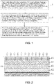
- the present invention provides a manufacturing method transparent OLED display, which comprises the following steps:
- Step 1 as shown in Figure 2 , providing a thin film transistor, TFT, array substrate 11, forming a cathode 12, an electron transport layer, ETL, 13, a light-emitting layer 14 and a hole transport layer (HTL) 15 sequentially on the TFT array substrate 11 to form a lower substrate 10.
- TFT thin film transistor
- ETL electron transport layer
- HTL hole transport layer
- the cathode 12 is a transparent electrode.
- the HTL 15 is made of an organic material with positive radicals.
- the positive radicals comprise at least one of NH 3 + and H + .
- a spin coating process or a spraying process is used to form the ETL 13 on the cathode 12; a spin coating process or an evaporation process is used to form the light-emitting layer 14 on the ETL 13, and a spin coating process or a spraying process is used to form the HTL 15 on the light-emitting layer 15.
- the materials of the ETL 13 comprise at least one of zinc oxide (ZnO) and poly [9,9-dioctafluorene-9,9-bis (N, N-dimethylaminopropyl) fluorene] (PFN).
- ZnO zinc oxide
- PPN poly [9,9-dioctafluorene-9,9-bis (N, N-dimethylaminopropyl) fluorene]
- the materials for the light-emitting layer 14 comprise organic light-emitting materials.
- Step 1 further comprises a step of forming an electron inject layer between the cathode 12 and the ETL 13.
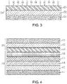
- Step 2 as shown in Figure 3 , providing an encapsulating cover plate 21, and forming an anode 22 and a hole inject layer, HIL, 23 on the encapsulating cover layer 21 sequentially to form an upper substrate 20.
- the anode 22 is a transparent electrode.
- the HIL 23 is made of an organic material with negative radicals.
- Step 1 and Step 2 are exchangeable.
- the negative radicals comprise at least one of COO - , OH - and Cl - .
- the materials of the cathode 12 and the materials of the anode 22 both comprise transparent conductive metal oxide, and the transparent conductive metal oxide is preferably indium tin oxide (ITO).
- ITO indium tin oxide
- the organic material with positive radicals in the HTL 15 and the organic material with negative radicals in the HIL 23 are respectively a hole transport material and a hole inject material commonly used in the known technology.
- the chemical treatment of these materials can be performed to made these materials carrying positive and negative radicals, respectively.
- the encapsulating cover plate 21 is a glass substrate or a plastic substrate.
- Step 3 laminating the upper substrate 20 and the lower substrate 10 in accordance with attaching the HTL 15 and the HIL 23 correspondingly, the positive radicals on the surface of the HTL 15 and the negative radicals on the surface of the HIL 23 mutually attracted by Coulomb force to create chemical reaction so that the upper substrate 20 and the lower substrate 10 being tightly attached to form a transparent OLED display.
- Step 3 is performed in a vacuum environment and under heated condition, and the temperature range is 100°C-400°C, and preferably, 200 °C.
- the heating can be performed by placing the upper substrate 20 on a heating plate, and placing the lower substrate 10 on top of the upper substrate 20, and followed by pressing together.
- Step 3 the heating of the upper substrate 20 and the lower substrate 10 can make the attachment of the upper substrate 20 and the lower substrate 10 tighter.
- the aforementioned manufacturing method by preparing the cathode 12 and the anode 22 on two different substrates, effectively avoids the destruction of the light-emitting layer 14 made of the organic light-emitting material caused by sputtering the anode 22 at the top of OLED and improves yield rate.
- the use of the transparent conductive metal oxide to manufacture the cathode 12 and the anode 22 of the OLED display provides an effective solution to the manufacturing of transparent OLED display which requires high conductivity and high transparency for the electrode material.
- the two substrates can be manufactured at the same time and then pressed to attach to achieve high manufacturing efficiency.
- the OLED display provided by the present invention is easy to manufacture and provides good performance.
- the present disclosure also provides a transparent OLED display, which comprises: an upper substrate 20 and a lower substrate 10 attached correspondingly.
- the upper substrate 20 further comprises: an encapsulating cover plate 21, an anode 22 disposed on the encapsulating plate 21, and a hole inject layer, HIL, 23 disposed on the anode 22.
- the lower substrate 10 comprises: a thin film transistor, TFT, array substrate 11, a cathode 12 disposed on the TFT array substrate 11, an electron transport layer, ETL, 13 disposed on the cathode 12, a light-emitting layer 14 disposed on the ETL 13, and a hole transport layer (HTL) 15 disposed on the light-emitting layer 14.
- Both the cathode 12 and anode 22 are transparent electrodes; the HTL 15 is made of an organic material with positive radicals; and the HIL 23 is made of an organic material with negative radicals.
- the upper substrate 20 and the lower substrate 10 are laminated in accordance with attaching the HTL 15 and the HIL 23 correspondingly.
- the positive radicals on the surface of the HTL 15 and the negative radicals on the surface of the HIL23 are mutually attracted by a Coulomb force to create a chemical reaction such that the upper substrate 20 and the lower substrate 10 are tightly attached to form a transparent OLED display.
- the positive radicals comprise at least one of NH 3 + and H +
- the negative radicals comprise at least one of COO - , OH - and Cl - .
- the materials of the cathode 12 and the materials of the anode 22 both comprise transparent conductive metal oxide, and the transparent conductive metal oxide is preferably indium tin oxide (ITO).
- ITO indium tin oxide
- the materials of the ETL 13 comprise at least one of zinc oxide (ZnO) and poly [9,9-dioctafluorene-9,9-bis (N, N-dimethylaminopropyl) fluorene] (PFN).
- ZnO zinc oxide
- PPN poly [9,9-dioctafluorene-9,9-bis (N, N-dimethylaminopropyl) fluorene]
- the materials for the light-emitting layer 14 comprise organic light-emitting materials.
- an electron inject layer is may be further formed between the cathode 12 and the ETL 13.
- the encapsulating cover plate 21 is a glass substrate or a plastic substrate.
- the aforementioned OLED display is easy to manufacture and provides good performance.
- an inverted (i.e., upside down) OLED structure is formed.
- the use of the inverted OLED structure can prolong the lifespan of the OLED display. This is because the inverted OLED structure uses ITO for the cathode 12. Compared to common OLED using a material such as aluminum, the ITO for the cathode 12 greatly improves the atmospheric stability of the cathode 12.
- the electron inject layer or the electron transport layer 13 above the cathode 12 can achieve oxygen- and water-resistant properties by using an inert material, which is particularly advantageous in a flexible OLED display because the necessity of using a high barrier hard encapsulating material is reduced.
- Another advantage of using an inverted OLED structure is that the driving stability of an active matrix (AM)-typed display using an n-type TFT is improved.
- AM active matrix
- the present invention provides a manufacturing method of transparent OLED display, by preparing the cathode and the anode on two different substrates to effectively avoid the destruction of the light-emitting layer made of the organic light-emitting material caused by sputtering the anode at the top of OLED to improve yield rate.
- the use of the transparent conductive metal oxide to manufacture the cathode and the anode of the OLED display provides an effective solution to the manufacturing of transparent OLED display which requires high conductivity and high transparency for the electrode material.
- the two substrates can be manufactured the same time and then pressed to attach to achieve high manufacturing efficiency.
- the OLED display obtained using the manufacturing method of the present invention is easy to manufacture and provides good performance.
Description
- The present invention relates to the field of display techniques, and in particular to a transparent OLED display and manufacturing method thereof.
- The organic light emitting diode (OLED) display, also called organic electroluminescent display, is the new trend of flat panel display technology. Because the OLED display provides the advantages of simple manufacturing process, low cost, low power-consumption, high illumination, wide operating temperature range, thin size, short response time, enabling full-color large display, easy to match integrated circuit (IC) driver, and enabling flexible display, the OLED is recognized as the technology with widest application prospect.
- The driving types of OLED can be divided according to the passive matrix OLED (PMOLED) and active matrix OLED (AMOLED), i.e., the direct addressable type and thin film transistor, TFT, addressable type, wherein the AMOLED provides the advantages of pixels arranged in an array, self-luminous, and high luminous efficiency and is commonly used for high definition large-size display.
- In general, the structure of an OLED display comprises: a substrate, an anode disposed on the substrate, a hole inject layer, HIL, disposed on the anode, a hole transport layer (HTL) disposed on the HIL, a light-emitting layer disposed on the HTL, an electron transport layer, ETL, disposed on the light-emitting layer, an electron inject layer (EIL) disposed on the ETL, and a cathode disposed on the EIL. The light-emission principle of the OLED display is that the semiconductor material and the organic light-emitting material emit light through the carrier injection and compound driven by an electric field. Specifically, the OLED display usually uses ITO pixel electrode and metal electrode respectively for the anode and cathode. Under a specific voltage driving, the electrons and holes are injected into the ETL and HTL respectively from the cathode and anode. The electrons and the holes are migrated respectively to the light-emitting layer and encounter each other to form excitons and excite the light-emitting molecules, which emit visible lights through radiation relaxation.
- As the technology rapidly progresses, the transparent display technology is proposed due to the novelty display means. The transparent display device allows the viewer to see the images displayed by the display and the actual background behind the display. The transparent display has many possible applications, such as, window display for building or vehicles. Other than those large-area applications, the transparent display is also applicable to handheld devices, such as, viewing a map while also viewing the view behind the display. The majority of current display market is estimated to be replaced by the transparent displays, for example, in building, advertisements, and public information applications.
- Compared to TFT-LCD, the OLED provides the advantages of the ability to realize large-sized, ultra-thin, flexible and transparent displays. The manufacturing of transparent OLED display needs to solve the problem of transparent electrodes as the material for transparent electrodes must provide higher conductivity and high penetration rate. The main material for transparent electrode currently is ITO, which is often manufactured by sputtering process. The sputtering process may damage the organic light-emitting layer of the OLED when a too-high power is applied, and suffers a too-long film forming time and low yield rate when a too-low power is applied.
-
US2005/009227A1 is a related prior art for this field. More particularly,US2005/009227A1 discloses a method to fabricate an organic electronic and opto-electronic device comprising: preparing a first part with at least a layer of a first organic material containing a first polymerisable group; preparing a second part with at least a layer of a second organic material containing a second polymerisable group; and bonding said first part to said second part under an environment with controlled parameters, wherein said bonding of said first part and said second part is achieved by cross-linking between said first polymerisable group and said second polymerisable groups.WO2006112537A1 is a related prior art for this field. More particularly,WO2006112537A1 discloses a method of manufacturing a semiconductor element which can produce a semiconductor element provided with a semiconductor layer having a high carrier transport ability, a semiconductor element manufactured by the semiconductor element manufacturing method, an electronic device provided with the semiconductor element, and electronic equipment having a high reliability.JP 2013222750A JP 2013222750A CN104966792A is a related prior art for this field. More particularly,CN104966792A discloses a composite film and a method for manufacturing the same, and an organic light-emitting diode and a method for packaging the same. The composite film comprises: a base membrane; a PDDA layer, which is deposited on a first surface of the base membrane; a graphite oxide layer, which is deposited on the PDDA layer; a monomolecular layer, which is self-assembled on a surface of the graphite oxide layer and is composed of a compound of Formula I. The method for manufacturing the composite film comprises a self-assembling step which includes placing and soaking a base membrane deposited with a graphite oxide layer in a solution of a compound of Formula I, and self-assembling the compound of Formula I on the graphite oxide layer. - The object of the present invention is to provide a manufacturing method of transparent OLED display to improve yield rate and production efficiency.
- Another object of the present disclosure is to provide a transparent OLED display, which is easy to manufacture and provides high performance.
- To achieve the above object, the present invention provides a manufacturing method of transparent OLED display, which comprises: Step 1: providing a thin film transistor, TFT, array substrate, forming a cathode, an electron transport layer, ETL, a light-emitting layer and a hole transport layer (HTL) sequentially on the TFT array substrate to form a lower substrate, wherein the cathode being a transparent electrode, the HTL being made of an organic material with positive radicals; Step 2: providing an encapsulating cover plate, and forming an anode and a hole inject layer, HIL, on the encapsulating cover layer sequentially to form an upper substrate, wherein the anode being a transparent electrode, the HIL being made of an organic material with negative radicals; execution order of
Step 1 andStep 2 being exchangeable; Step 3: laminating the upper substrate and the lower substrate in accordance with attaching the HTL and the HIL correspondingly, the positive radicals on the surface of the HTL and the negative radicals on the surface of the HIL being mutually attracted by Coulomb force to create a chemical reaction such that the upper substrate and the lower substrate are tightly attached to form a transparent OLED display. According to a preferred embodiment of the present invention, the positive radicals comprise at least one of NH3 + and H+, and the negative radicals comprise at least one of COO-, OH- and Cl-. - According to a preferred embodiment of the present invention, in
Step 1, a spin coating process or a spraying process is used to form the ETL on the cathode; a spin coating process or an evaporation process is used to form the light-emitting layer on the ETL, and a spin coating process or a spraying process is used to form the HTL on the light-emitting layer. - According to a preferred embodiment of the present invention, the materials of the cathode and the materials of the anode both comprise transparent conductive metal oxide.
- According to a preferred embodiment of the present invention, the materials of the ETL comprise at least one of zinc oxide and poly [9,9-dioctafluorene-9,9-bis (N, N-dimethylaminopropyl) fluorene].
- According to a preferred embodiment of the present invention,
Step 3 is performed in a vacuum environment and under heated condition, and the temperature range is 100°C-400°C. - Another embodiment of the present disclosure provides a transparent OLED display, which comprises: an upper substrate and a lower substrate attached correspondingly; the upper substrate further comprising: an encapsulating cover plate, an anode disposed on the encapsulating plate, and a hole inject layer, HIL, disposed on the anode; the lower substrate comprising: a thin film transistor, TFT, array substrate, a cathode disposed on the TFT array substrate, an electron transport layer, ETL, disposed on the cathode, a light-emitting layer disposed on the ETL, and a hole transport layer (HTL) disposed on the light-emitting layer; both the cathode and anode being transparent electrodes; the HTL being made of an organic material with positive radicals; the HIL being made of an organic material with negative radicals; wherein the upper substrate and the lower substrate being laminated in accordance with attaching the HTL and the HIL correspondingly, the positive radicals on the surface of the HTL and the negative radicals on the surface of the HIL being mutually attracted by a Coulomb force to create a chemical reaction such that the upper substrate and the lower substrate are tightly attached to form a transparent OLED display.
- According to a preferred embodiment of the present disclosure, the positive radicals comprise at least one of NH3 + and H+, and the negative radicals comprise at least one of COO-, OH- and Cl-.
- According to a preferred embodiment of the present disclosure, the materials of the cathode and the materials of the anode both comprise transparent conductive metal oxide.
- According to a preferred embodiment of the present disclosure, the materials of the ETL comprise at least one of zinc oxide and poly [9,9-dioctafluorene-9,9-bis (N, N-dimethylaminopropyl) fluorene].
- According to a preferred embodiment of the present invention, the positive radicals comprise at least one of NH3 + and H+, and the negative radicals comprise at least one of COO-, OH- and Cl-; wherein, in
Step 1, a spin coating process or a spraying process is used to form the ETL on the cathode; a spin coating process or an evaporation process is used to form the light-emitting layer on the ETL, and a spin coating process or a spraying process is used to form the HTL on the light-emitting layer. - Compared to the known techniques, the present invention provides the following advantages. The present invention provides a manufacturing method of transparent OLED display, by preparing the cathode and the anode on two different substrates to effectively avoid the destruction of the light-emitting layer made of the organic light-emitting material caused by sputtering the anode at the top of OLED to improve yield rate. The use of the transparent conductive metal oxide to manufacture the cathode and the anode of the OLED display provides an effective solution to the manufacturing of transparent OLED display which requires high conductivity and high transparency for the electrode material. In addition, the two substrates can be manufactured the same time and then pressed to attach to achieve high manufacturing efficiency. The OLED display provided by the present invention is easy to manufacture and provides good performance.
- To make the technical solution of the embodiments according to the present invention, a brief description of the drawings that are necessary for the illustration of the embodiments will be given as follows. Apparently, the drawings described below show only example embodiments of the present invention and for those having ordinary skills in the art, other drawings may be easily obtained from these drawings without paying any creative effort. In the drawings:
-
Figure 1 is a schematic view showing the flowchart of the manufacturing method of OLED display provided by an embodiment of the present invention; -
Figure 2 is a schematic view showingStep 1 of the manufacturing method of OLED display provided by an embodiment of the present invention; -
Figure 3 is a schematic view showingStep 2 of the manufacturing method of OLED display provided by an embodiment of the present invention; and -
Figure 4 is a schematic view showingStep 3 of the manufacturing method of OLED display provided by an embodiment of the present invention, and the structure of the transparent OLED display provided by an embodiment of the present disclosure. - Referring to
Figure 1 , the present invention provides a manufacturing method transparent OLED display, which comprises the following steps: - Step 1: as shown in
Figure 2 , providing a thin film transistor, TFT,array substrate 11, forming acathode 12, an electron transport layer, ETL, 13, a light-emitting layer 14 and a hole transport layer (HTL) 15 sequentially on theTFT array substrate 11 to form alower substrate 10. - The
cathode 12 is a transparent electrode. - The HTL 15 is made of an organic material with positive radicals.
- Preferably, the positive radicals comprise at least one of NH3 + and H+.
- Specifically, a spin coating process or a spraying process is used to form the
ETL 13 on thecathode 12; a spin coating process or an evaporation process is used to form the light-emittinglayer 14 on theETL 13, and a spin coating process or a spraying process is used to form theHTL 15 on the light-emittinglayer 15. - Preferably, the materials of the
ETL 13 comprise at least one of zinc oxide (ZnO) and poly [9,9-dioctafluorene-9,9-bis (N, N-dimethylaminopropyl) fluorene] (PFN). - Specifically, the materials for the light-emitting
layer 14 comprise organic light-emitting materials. - Optionally,
Step 1 further comprises a step of forming an electron inject layer between thecathode 12 and theETL 13. - Step 2: as shown in
Figure 3 , providing an encapsulatingcover plate 21, and forming ananode 22 and a hole inject layer, HIL, 23 on the encapsulatingcover layer 21 sequentially to form anupper substrate 20. - The
anode 22 is a transparent electrode. - The
HIL 23 is made of an organic material with negative radicals. - Specifically, the execution order of
Step 1 andStep 2 is exchangeable. - Preferably, the negative radicals comprise at least one of COO-, OH- and Cl-.
- Specifically, the materials of the
cathode 12 and the materials of theanode 22 both comprise transparent conductive metal oxide, and the transparent conductive metal oxide is preferably indium tin oxide (ITO). - Specifically, the organic material with positive radicals in the
HTL 15 and the organic material with negative radicals in theHIL 23 are respectively a hole transport material and a hole inject material commonly used in the known technology. The chemical treatment of these materials can be performed to made these materials carrying positive and negative radicals, respectively. - Specifically, the encapsulating
cover plate 21 is a glass substrate or a plastic substrate. - Step 3: as shown in
Figure 4 , laminating theupper substrate 20 and thelower substrate 10 in accordance with attaching theHTL 15 and theHIL 23 correspondingly, the positive radicals on the surface of theHTL 15 and the negative radicals on the surface of theHIL 23 mutually attracted by Coulomb force to create chemical reaction so that theupper substrate 20 and thelower substrate 10 being tightly attached to form a transparent OLED display. - Preferably,
Step 3 is performed in a vacuum environment and under heated condition, and the temperature range is 100°C-400°C, and preferably, 200 °C. The heating can be performed by placing theupper substrate 20 on a heating plate, and placing thelower substrate 10 on top of theupper substrate 20, and followed by pressing together. - Specifically, in
Step 3, the heating of theupper substrate 20 and thelower substrate 10 can make the attachment of theupper substrate 20 and thelower substrate 10 tighter. - The aforementioned manufacturing method, by preparing the
cathode 12 and theanode 22 on two different substrates, effectively avoids the destruction of the light-emittinglayer 14 made of the organic light-emitting material caused by sputtering theanode 22 at the top of OLED and improves yield rate. The use of the transparent conductive metal oxide to manufacture thecathode 12 and theanode 22 of the OLED display provides an effective solution to the manufacturing of transparent OLED display which requires high conductivity and high transparency for the electrode material. In addition, the two substrates can be manufactured at the same time and then pressed to attach to achieve high manufacturing efficiency. The OLED display provided by the present invention is easy to manufacture and provides good performance. - Referring to
Figure 4 , based on the aforementioned manufacturing method of transparent OLED display, the present disclosure also provides a transparent OLED display, which comprises: anupper substrate 20 and alower substrate 10 attached correspondingly. Theupper substrate 20 further comprises: an encapsulatingcover plate 21, ananode 22 disposed on the encapsulatingplate 21, and a hole inject layer, HIL, 23 disposed on theanode 22. - The
lower substrate 10 comprises: a thin film transistor, TFT,array substrate 11, acathode 12 disposed on theTFT array substrate 11, an electron transport layer, ETL, 13 disposed on thecathode 12, a light-emittinglayer 14 disposed on theETL 13, and a hole transport layer (HTL) 15 disposed on the light-emittinglayer 14. - Both the
cathode 12 andanode 22 are transparent electrodes; theHTL 15 is made of an organic material with positive radicals; and theHIL 23 is made of an organic material with negative radicals. - The
upper substrate 20 and thelower substrate 10 are laminated in accordance with attaching theHTL 15 and theHIL 23 correspondingly. The positive radicals on the surface of theHTL 15 and the negative radicals on the surface of the HIL23 are mutually attracted by a Coulomb force to create a chemical reaction such that theupper substrate 20 and thelower substrate 10 are tightly attached to form a transparent OLED display. - Preferably, the positive radicals comprise at least one of NH3 + and H+, and the negative radicals comprise at least one of COO-, OH- and Cl-.
- Preferably, the materials of the
cathode 12 and the materials of theanode 22 both comprise transparent conductive metal oxide, and the transparent conductive metal oxide is preferably indium tin oxide (ITO). - Preferably, the materials of the
ETL 13 comprise at least one of zinc oxide (ZnO) and poly [9,9-dioctafluorene-9,9-bis (N, N-dimethylaminopropyl) fluorene] (PFN). - Specifically, the materials for the light-emitting
layer 14 comprise organic light-emitting materials. - Specifically, in the
lower substrate 10, an electron inject layer is may be further formed between thecathode 12 and theETL 13. - Specifically, the encapsulating
cover plate 21 is a glass substrate or a plastic substrate. - The aforementioned OLED display is easy to manufacture and provides good performance. In addition, by disposing the
cathode 12 on theTFT array substrate 11, and the top electrode provided as theanode 22, an inverted (i.e., upside down) OLED structure is formed. The use of the inverted OLED structure can prolong the lifespan of the OLED display. This is because the inverted OLED structure uses ITO for thecathode 12. Compared to common OLED using a material such as aluminum, the ITO for thecathode 12 greatly improves the atmospheric stability of thecathode 12. In addition, the electron inject layer or theelectron transport layer 13 above thecathode 12 can achieve oxygen- and water-resistant properties by using an inert material, which is particularly advantageous in a flexible OLED display because the necessity of using a high barrier hard encapsulating material is reduced. Another advantage of using an inverted OLED structure is that the driving stability of an active matrix (AM)-typed display using an n-type TFT is improved. - In summary, the present invention provides a manufacturing method of transparent OLED display, by preparing the cathode and the anode on two different substrates to effectively avoid the destruction of the light-emitting layer made of the organic light-emitting material caused by sputtering the anode at the top of OLED to improve yield rate. The use of the transparent conductive metal oxide to manufacture the cathode and the anode of the OLED display provides an effective solution to the manufacturing of transparent OLED display which requires high conductivity and high transparency for the electrode material. In addition, the two substrates can be manufactured the same time and then pressed to attach to achieve high manufacturing efficiency. The OLED display obtained using the manufacturing method of the present invention is easy to manufacture and provides good performance.
- It should be noted that in the present disclosure the terms, such as, first, second are only for distinguishing an entity or operation from another entity or operation, and does not imply any specific relation or order between the entities or operations. Also, the terms "comprises", "include", and other similar variations, do not exclude the inclusion of other non-listed elements. Without further restrictions, the expression "comprises a..." does not exclude other identical elements from presence besides the listed elements.
- Embodiments of the present invention have been described, but not intending to impose any unduly constraint to the appended claims. Any modification made according to the disclosure and drawings of the present invention, or any application thereof, directly or indirectly, to other related fields of technique, is considered encompassed in the scope of protection defined by the clams of the present invention.
Claims (10)
- A manufacturing method of a transparent organic light-emitting diode, OLED, display, the method comprising:Step 1: providing a thin film transistor, TFT, array substrate (11), forming a cathode (12), an electron transport layer, ETL (13), a light-emitting layer (14) and a hole transport layer (15), HTL, sequentially on the TFT array substrate (11) to form a lower substrate (10), wherein the cathode (12) being a transparent electrode, the HTL (15) being made of an organic material with positive radicals;Step 2: providing an encapsulating cover plate (21), and forming an anode (22) and a hole inject layer, HIL (23), on the encapsulating cover layer sequentially to form an upper substrate (20), wherein the anode (22) being a transparent electrode, the HIL (23) being made of an organic material with negative radicals; execution order of Step 1 and Step 2 being exchangeable;Step 3: laminating the upper substrate (20) and the lower substrate (10) in accordance with attaching the HTL (15) and the HIL (23) correspondingly, the positive radicals on the surface of the HTL (15) and the negative radicals on the surface of the HIL (23) being mutually attracted by a Coulomb force to create a chemical reaction such that the upper substrate (20) and the lower substrate (10) are tightly attached to form the transparent OLED display.
- The manufacturing method of transparent OLED as claimed in Claim 1, wherein the positive radicals comprise at least one of NH3 + and H+, and the negative radicals comprise at least one of COO-, OH- and Cl-.
- The manufacturing method of transparent OLED as claimed in Claim 1, wherein in Step 1, a spin coating process or a spraying process is used to form the ETL (13) on the cathode (12); a spin coating process or an evaporation process is used to form the light-emitting layer (14) on the ETL (13), and a spin coating process or a spraying process is used to form the HTL (15) on the light-emitting layer (14).
- The manufacturing method of transparent OLED as claimed in Claim 1, wherein the materials of the cathode (12) and the materials of the anode (22) both comprise transparent conductive metal oxide.
- The manufacturing method of transparent OLED as claimed in Claim 1, wherein the materials of the ETL (13) comprise at least one of zinc oxide and poly [9,9-dioctafluorene-9,9-bis (N, N-dimethylaminopropyl) fluorene].
- The manufacturing method of transparent OLED as claimed in Claim 1, wherein Step 3 is performed in a vacuum environment and under heated condition, and the temperature range is 100°C-400°C.
- The manufacturing method of transparent organic light-emitting diode (OLED) display, according to claim 1, wherein the positive radicals comprise at least one of NH3+ and H+, and the negative radicals comprise at least one of COO-, OH- and Cl-, and
in Step 1, a spin coating process or a spraying process is used to form the ETL (13) on the cathode (12); a spin coating process or an evaporation process is used to form the light-emitting layer (14) on the ETL (13), and a spin coating process or a spraying process is used to form the HTL (15) on the light-emitting layer (14). - The manufacturing method of transparent OLED as claimed in Claim 7, wherein the materials of the cathode (12) and the materials of the anode (22) both comprise transparent conductive metal oxide.
- The manufacturing method of transparent OLED as claimed in any one of Claims 7-8, wherein the materials of the ETL (13) comprise at least one of zinc oxide and poly [9,9-dioctafluorene-9,9-bis (N, N-dimethylaminopropyl) fluorene].
- The manufacturing method of transparent OLED as claimed in any one of Claims 7-9, wherein Step 3 is performed in a vacuum environment and under heated condition, and the temperature range is 100°C-400°C.
Applications Claiming Priority (2)
| Application Number | Priority Date | Filing Date | Title |
|---|---|---|---|
| CN201610891514.XA CN106450015B (en) | 2016-10-11 | 2016-10-11 | Transparent OLED display and preparation method thereof |
| PCT/CN2016/109567 WO2018068379A1 (en) | 2016-10-11 | 2016-12-13 | Transparent oled display and manufacturing method therefor |
Publications (3)
| Publication Number | Publication Date |
|---|---|
| EP3528299A1 EP3528299A1 (en) | 2019-08-21 |
| EP3528299A4 EP3528299A4 (en) | 2020-06-24 |
| EP3528299B1 true EP3528299B1 (en) | 2022-11-09 |
Family
ID=58174719
Family Applications (1)
| Application Number | Title | Priority Date | Filing Date |
|---|---|---|---|
| EP16918595.6A Active EP3528299B1 (en) | 2016-10-11 | 2016-12-13 | Manufacturing method of a transparent oled display |
Country Status (7)
| Country | Link |
|---|---|
| US (1) | US10211399B2 (en) |
| EP (1) | EP3528299B1 (en) |
| JP (1) | JP6910432B2 (en) |
| KR (1) | KR102135217B1 (en) |
| CN (1) | CN106450015B (en) |
| PL (1) | PL3528299T3 (en) |
| WO (1) | WO2018068379A1 (en) |
Families Citing this family (9)
| Publication number | Priority date | Publication date | Assignee | Title |
|---|---|---|---|---|
| CN105355798A (en) * | 2015-11-25 | 2016-02-24 | 京东方科技集团股份有限公司 | Organic electroluminescent device, manufacturing method thereof, and display device |
| CN107302059A (en) * | 2017-06-13 | 2017-10-27 | 深圳市华星光电技术有限公司 | A kind of flexible OLED and preparation method thereof |
| KR102418612B1 (en) | 2018-01-03 | 2022-07-08 | 엘지전자 주식회사 | Mobile terminal |
| CN109244260B (en) * | 2018-09-19 | 2021-01-29 | 京东方科技集团股份有限公司 | Preparation method of display panel |
| CN109545991B (en) * | 2018-10-24 | 2021-10-26 | 东北石油大学 | Application of gold nano bipyramid in OLED device |
| CN109545827A (en) * | 2018-11-21 | 2019-03-29 | 惠科股份有限公司 | Display panel and display device |
| CN109683379A (en) * | 2019-01-25 | 2019-04-26 | 京东方科技集团股份有限公司 | Color membrane structure, color membrane substrates, display panel and display device |
| CN109801950B (en) * | 2019-01-31 | 2021-02-26 | 厦门天马微电子有限公司 | Display panel, display device and manufacturing method of display panel |
| KR20220083179A (en) | 2020-12-11 | 2022-06-20 | 차영서 | OLED license plate |
Citations (1)
| Publication number | Priority date | Publication date | Assignee | Title |
|---|---|---|---|---|
| CN104966792A (en) * | 2015-07-17 | 2015-10-07 | 京东方科技集团股份有限公司 | Composite thin film and manufacturing method, organic light emitting diode and packaging method |
Family Cites Families (18)
| Publication number | Priority date | Publication date | Assignee | Title |
|---|---|---|---|---|
| DE69831243T2 (en) * | 1998-10-13 | 2006-08-10 | Sony Deutschland Gmbh | A manufacturing method of an active matrix light-emitting display device |
| US7063994B2 (en) * | 2003-07-11 | 2006-06-20 | Organic Vision Inc. | Organic semiconductor devices and methods of fabrication including forming two parts with polymerisable groups and bonding the parts |
| KR20050029426A (en) * | 2003-09-22 | 2005-03-28 | 삼성에스디아이 주식회사 | Full color oled having color filter layer or color conversion medium |
| WO2006019270A1 (en) * | 2004-08-19 | 2006-02-23 | Lg Chem. Ltd. | Organic light-emitting device comprising buffer layer and method for fabricating the same |
| JP2006302556A (en) * | 2005-04-18 | 2006-11-02 | Seiko Epson Corp | Manufacturing method of semiconductor device, semiconductor device, electronic device, and electronic apparatus |
| KR101413233B1 (en) * | 2007-09-14 | 2014-06-30 | 삼성전자 주식회사 | Nano-imprint lithography process |
| US20090130296A1 (en) * | 2007-11-15 | 2009-05-21 | Universal Display Corporation | Fabrication of Organic Electronic Devices by Ink-Jet Printing at Low Temperatures |
| CN101777577B (en) * | 2010-03-10 | 2012-01-04 | 彩虹集团公司 | Color organic light emitting display panel and manufacturing method thereof |
| CN103120020B (en) * | 2010-07-21 | 2016-03-23 | 住友化学株式会社 | The manufacture method of organic electroluminescent device |
| JP5706180B2 (en) * | 2011-02-15 | 2015-04-22 | 常陽工学株式会社 | Sealing method and apparatus |
| KR101218651B1 (en) * | 2011-12-30 | 2013-01-21 | 한국과학기술원 | Organic light emitting device and method for the same |
| JP2013184346A (en) * | 2012-03-07 | 2013-09-19 | Asahi Glass Co Ltd | Glass laminate, and method for producing electronic device |
| JP2013222750A (en) * | 2012-04-13 | 2013-10-28 | Kuraray Co Ltd | Photoelectric conversion element, method for manufacturing the same, and solar cell |
| KR20140000565A (en) * | 2012-06-25 | 2014-01-03 | 삼성디스플레이 주식회사 | Donor substrate, method of laser induced thermal imaging using a donor substrate and method of manufacturing an organic light emitting display device using a donor substrate |
| TWI690585B (en) * | 2014-08-11 | 2020-04-11 | 德商漢高股份有限及兩合公司 | Electroluminescent crosslinked nanocrystal films |
| KR102354969B1 (en) * | 2015-02-05 | 2022-01-25 | 삼성디스플레이 주식회사 | Organic light emitting display apparatus |
| US20170324049A1 (en) * | 2016-05-05 | 2017-11-09 | Universal Display Corporation | Organic Electroluminescent Materials and Devices |
| US10964893B2 (en) * | 2016-11-17 | 2021-03-30 | Universal Display Corporation | Organic electroluminescent materials and devices |
-
2016
- 2016-10-11 CN CN201610891514.XA patent/CN106450015B/en active Active
- 2016-12-13 JP JP2019519397A patent/JP6910432B2/en active Active
- 2016-12-13 KR KR1020197013492A patent/KR102135217B1/en active IP Right Grant
- 2016-12-13 PL PL16918595.6T patent/PL3528299T3/en unknown
- 2016-12-13 US US15/326,639 patent/US10211399B2/en active Active
- 2016-12-13 EP EP16918595.6A patent/EP3528299B1/en active Active
- 2016-12-13 WO PCT/CN2016/109567 patent/WO2018068379A1/en active Application Filing
Patent Citations (1)
| Publication number | Priority date | Publication date | Assignee | Title |
|---|---|---|---|---|
| CN104966792A (en) * | 2015-07-17 | 2015-10-07 | 京东方科技集团股份有限公司 | Composite thin film and manufacturing method, organic light emitting diode and packaging method |
Also Published As
| Publication number | Publication date |
|---|---|
| CN106450015B (en) | 2018-07-10 |
| CN106450015A (en) | 2017-02-22 |
| JP6910432B2 (en) | 2021-07-28 |
| JP2019537201A (en) | 2019-12-19 |
| WO2018068379A1 (en) | 2018-04-19 |
| US20180337336A1 (en) | 2018-11-22 |
| US10211399B2 (en) | 2019-02-19 |
| PL3528299T3 (en) | 2023-01-23 |
| KR102135217B1 (en) | 2020-07-17 |
| KR20190058649A (en) | 2019-05-29 |
| EP3528299A4 (en) | 2020-06-24 |
| EP3528299A1 (en) | 2019-08-21 |
Similar Documents
| Publication | Publication Date | Title |
|---|---|---|
| EP3528299B1 (en) | Manufacturing method of a transparent oled display | |
| US10811479B2 (en) | Flexible TFT substrate having a plurality of grooves in organic layer | |
| TWI231153B (en) | Organic electroluminescence display device and its fabrication method | |
| CN100530752C (en) | Organic electro luminescence device and fabrication method thereof | |
| US10290688B2 (en) | AMOLED device and manufacturing method thereof | |
| US20180198094A1 (en) | Manufacturing method of flexible oled display panel | |
| CN102544056A (en) | Organic light emitting diode display and manufacturing method of the same | |
| CN106449711A (en) | Flexible AMOLED display device preparation method | |
| US10243163B2 (en) | Flexible OLED display and manufacturing method thereof | |
| CN104538420A (en) | Flexible oled display device and manufacturing method thereof | |
| US20150171376A1 (en) | Method for manufacturing flexible oled (organic light emitting diode) panel | |
| KR20080054626A (en) | Organic electro luminescence display device and fabricating method thereof | |
| WO2019090837A1 (en) | Double-sided display, and manufacturing method thereof | |
| CN104538421A (en) | OLED display substrate and manufacturing method of OLED display substrate | |
| WO2019041578A1 (en) | Oled substrate and manufacturing method therefor | |
| CN109659344B (en) | Flexible OLED device | |
| WO2020237952A1 (en) | Double-sided display panel and preparation method thereof, and display apparatus | |
| CN108565351B (en) | OLED display device and manufacturing method thereof | |
| KR20110017715A (en) | Organic light emitting display apparatus and method of manufacturing the same | |
| KR101015887B1 (en) | Organic light emitting display apparatus | |
| US20200381501A1 (en) | Double-sided display panel, fabricating method of same, and display device | |
| KR20120110777A (en) | Organic light emitting device | |
| CN110085652B (en) | OLED substrate | |
| KR20040106923A (en) | Apparatus and method of employing self-assembled molecules to function as an electron injection layer of oled | |
| KR100961954B1 (en) | The Method For Fabricating Organic Light Emitting Display |
Legal Events
| Date | Code | Title | Description |
|---|---|---|---|
| STAA | Information on the status of an ep patent application or granted ep patent |
Free format text: STATUS: THE INTERNATIONAL PUBLICATION HAS BEEN MADE |
|
| PUAI | Public reference made under article 153(3) epc to a published international application that has entered the european phase |
Free format text: ORIGINAL CODE: 0009012 |
|
| STAA | Information on the status of an ep patent application or granted ep patent |
Free format text: STATUS: REQUEST FOR EXAMINATION WAS MADE |
|
| 17P | Request for examination filed |
Effective date: 20190503 |
|
| AK | Designated contracting states |
Kind code of ref document: A1 Designated state(s): AL AT BE BG CH CY CZ DE DK EE ES FI FR GB GR HR HU IE IS IT LI LT LU LV MC MK MT NL NO PL PT RO RS SE SI SK SM TR |
|
| AX | Request for extension of the european patent |
Extension state: BA ME |
|
| DAV | Request for validation of the european patent (deleted) | ||
| DAX | Request for extension of the european patent (deleted) | ||
| REG | Reference to a national code |
Ref country code: DE Ref legal event code: R079 Ref document number: 602016076297 Country of ref document: DE Free format text: PREVIOUS MAIN CLASS: H01L0051500000 Ipc: H01L0051520000 |
|
| A4 | Supplementary search report drawn up and despatched |
Effective date: 20200526 |
|
| RIC1 | Information provided on ipc code assigned before grant |
Ipc: H01L 51/52 20060101AFI20200518BHEP Ipc: H01L 51/56 20060101ALI20200518BHEP |
|
| STAA | Information on the status of an ep patent application or granted ep patent |
Free format text: STATUS: EXAMINATION IS IN PROGRESS |
|
| 17Q | First examination report despatched |
Effective date: 20220104 |
|
| INTG | Intention to grant announced |
Effective date: 20220721 |
|
| RIN1 | Information on inventor provided before grant (corrected) |
Inventor name: XU, CHAO |
|
| GRAS | Grant fee paid |
Free format text: ORIGINAL CODE: EPIDOSNIGR3 |
|
| STAA | Information on the status of an ep patent application or granted ep patent |
Free format text: STATUS: GRANT OF PATENT IS INTENDED |
|
| GRAA | (expected) grant |
Free format text: ORIGINAL CODE: 0009210 |
|
| STAA | Information on the status of an ep patent application or granted ep patent |
Free format text: STATUS: THE PATENT HAS BEEN GRANTED |
|
| AK | Designated contracting states |
Kind code of ref document: B1 Designated state(s): AL AT BE BG CH CY CZ DE DK EE ES FI FR GB GR HR HU IE IS IT LI LT LU LV MC MK MT NL NO PL PT RO RS SE SI SK SM TR |
|
| RAP3 | Party data changed (applicant data changed or rights of an application transferred) |
Owner name: WUHAN CHINA STAR OPTOELECTRONICS TECHNOLOGY CO., LTD. |
|
| REG | Reference to a national code |
Ref country code: GB Ref legal event code: FG4D |
|
| REG | Reference to a national code |
Ref country code: CH Ref legal event code: EP Ref country code: AT Ref legal event code: REF Ref document number: 1530948 Country of ref document: AT Kind code of ref document: T Effective date: 20221115 |
|
| REG | Reference to a national code |
Ref country code: DE Ref legal event code: R079 Ref document number: 602016076297 Country of ref document: DE Free format text: PREVIOUS MAIN CLASS: H01L0051520000 Ipc: H10K0050800000 |
|
| REG | Reference to a national code |
Ref country code: DE Ref legal event code: R096 Ref document number: 602016076297 Country of ref document: DE |
|
| REG | Reference to a national code |
Ref country code: IE Ref legal event code: FG4D |
|
| REG | Reference to a national code |
Ref country code: LT Ref legal event code: MG9D |
|
| REG | Reference to a national code |
Ref country code: NL Ref legal event code: MP Effective date: 20221109 |
|
| REG | Reference to a national code |
Ref country code: AT Ref legal event code: MK05 Ref document number: 1530948 Country of ref document: AT Kind code of ref document: T Effective date: 20221109 |
|
| PG25 | Lapsed in a contracting state [announced via postgrant information from national office to epo] |
Ref country code: SE Free format text: LAPSE BECAUSE OF FAILURE TO SUBMIT A TRANSLATION OF THE DESCRIPTION OR TO PAY THE FEE WITHIN THE PRESCRIBED TIME-LIMIT Effective date: 20221109 Ref country code: PT Free format text: LAPSE BECAUSE OF FAILURE TO SUBMIT A TRANSLATION OF THE DESCRIPTION OR TO PAY THE FEE WITHIN THE PRESCRIBED TIME-LIMIT Effective date: 20230309 Ref country code: NO Free format text: LAPSE BECAUSE OF FAILURE TO SUBMIT A TRANSLATION OF THE DESCRIPTION OR TO PAY THE FEE WITHIN THE PRESCRIBED TIME-LIMIT Effective date: 20230209 Ref country code: LT Free format text: LAPSE BECAUSE OF FAILURE TO SUBMIT A TRANSLATION OF THE DESCRIPTION OR TO PAY THE FEE WITHIN THE PRESCRIBED TIME-LIMIT Effective date: 20221109 Ref country code: FI Free format text: LAPSE BECAUSE OF FAILURE TO SUBMIT A TRANSLATION OF THE DESCRIPTION OR TO PAY THE FEE WITHIN THE PRESCRIBED TIME-LIMIT Effective date: 20221109 Ref country code: ES Free format text: LAPSE BECAUSE OF FAILURE TO SUBMIT A TRANSLATION OF THE DESCRIPTION OR TO PAY THE FEE WITHIN THE PRESCRIBED TIME-LIMIT Effective date: 20221109 Ref country code: AT Free format text: LAPSE BECAUSE OF FAILURE TO SUBMIT A TRANSLATION OF THE DESCRIPTION OR TO PAY THE FEE WITHIN THE PRESCRIBED TIME-LIMIT Effective date: 20221109 |
|
| PG25 | Lapsed in a contracting state [announced via postgrant information from national office to epo] |
Ref country code: RS Free format text: LAPSE BECAUSE OF FAILURE TO SUBMIT A TRANSLATION OF THE DESCRIPTION OR TO PAY THE FEE WITHIN THE PRESCRIBED TIME-LIMIT Effective date: 20221109 Ref country code: LV Free format text: LAPSE BECAUSE OF FAILURE TO SUBMIT A TRANSLATION OF THE DESCRIPTION OR TO PAY THE FEE WITHIN THE PRESCRIBED TIME-LIMIT Effective date: 20221109 Ref country code: IS Free format text: LAPSE BECAUSE OF FAILURE TO SUBMIT A TRANSLATION OF THE DESCRIPTION OR TO PAY THE FEE WITHIN THE PRESCRIBED TIME-LIMIT Effective date: 20230309 Ref country code: HR Free format text: LAPSE BECAUSE OF FAILURE TO SUBMIT A TRANSLATION OF THE DESCRIPTION OR TO PAY THE FEE WITHIN THE PRESCRIBED TIME-LIMIT Effective date: 20221109 Ref country code: GR Free format text: LAPSE BECAUSE OF FAILURE TO SUBMIT A TRANSLATION OF THE DESCRIPTION OR TO PAY THE FEE WITHIN THE PRESCRIBED TIME-LIMIT Effective date: 20230210 |
|
| PGFP | Annual fee paid to national office [announced via postgrant information from national office to epo] |
Ref country code: PL Payment date: 20221229 Year of fee payment: 7 |
|
| PG25 | Lapsed in a contracting state [announced via postgrant information from national office to epo] |
Ref country code: NL Free format text: LAPSE BECAUSE OF FAILURE TO SUBMIT A TRANSLATION OF THE DESCRIPTION OR TO PAY THE FEE WITHIN THE PRESCRIBED TIME-LIMIT Effective date: 20221109 |
|
| P01 | Opt-out of the competence of the unified patent court (upc) registered |
Effective date: 20230530 |
|
| PG25 | Lapsed in a contracting state [announced via postgrant information from national office to epo] |
Ref country code: SM Free format text: LAPSE BECAUSE OF FAILURE TO SUBMIT A TRANSLATION OF THE DESCRIPTION OR TO PAY THE FEE WITHIN THE PRESCRIBED TIME-LIMIT Effective date: 20221109 Ref country code: RO Free format text: LAPSE BECAUSE OF FAILURE TO SUBMIT A TRANSLATION OF THE DESCRIPTION OR TO PAY THE FEE WITHIN THE PRESCRIBED TIME-LIMIT Effective date: 20221109 Ref country code: EE Free format text: LAPSE BECAUSE OF FAILURE TO SUBMIT A TRANSLATION OF THE DESCRIPTION OR TO PAY THE FEE WITHIN THE PRESCRIBED TIME-LIMIT Effective date: 20221109 Ref country code: DK Free format text: LAPSE BECAUSE OF FAILURE TO SUBMIT A TRANSLATION OF THE DESCRIPTION OR TO PAY THE FEE WITHIN THE PRESCRIBED TIME-LIMIT Effective date: 20221109 Ref country code: CZ Free format text: LAPSE BECAUSE OF FAILURE TO SUBMIT A TRANSLATION OF THE DESCRIPTION OR TO PAY THE FEE WITHIN THE PRESCRIBED TIME-LIMIT Effective date: 20221109 |
|
| REG | Reference to a national code |
Ref country code: CH Ref legal event code: PL |
|
| REG | Reference to a national code |
Ref country code: DE Ref legal event code: R097 Ref document number: 602016076297 Country of ref document: DE |
|
| REG | Reference to a national code |
Ref country code: BE Ref legal event code: MM Effective date: 20221231 |
|
| PG25 | Lapsed in a contracting state [announced via postgrant information from national office to epo] |
Ref country code: SK Free format text: LAPSE BECAUSE OF FAILURE TO SUBMIT A TRANSLATION OF THE DESCRIPTION OR TO PAY THE FEE WITHIN THE PRESCRIBED TIME-LIMIT Effective date: 20221109 Ref country code: AL Free format text: LAPSE BECAUSE OF FAILURE TO SUBMIT A TRANSLATION OF THE DESCRIPTION OR TO PAY THE FEE WITHIN THE PRESCRIBED TIME-LIMIT Effective date: 20221109 Ref country code: LU Free format text: LAPSE BECAUSE OF NON-PAYMENT OF DUE FEES Effective date: 20221213 |
|
| PLBE | No opposition filed within time limit |
Free format text: ORIGINAL CODE: 0009261 |
|
| STAA | Information on the status of an ep patent application or granted ep patent |
Free format text: STATUS: NO OPPOSITION FILED WITHIN TIME LIMIT |
|
| 26N | No opposition filed |
Effective date: 20230810 |
|
| PG25 | Lapsed in a contracting state [announced via postgrant information from national office to epo] |
Ref country code: LI Free format text: LAPSE BECAUSE OF NON-PAYMENT OF DUE FEES Effective date: 20221231 Ref country code: IE Free format text: LAPSE BECAUSE OF NON-PAYMENT OF DUE FEES Effective date: 20221213 Ref country code: CH Free format text: LAPSE BECAUSE OF NON-PAYMENT OF DUE FEES Effective date: 20221231 |
|
| PG25 | Lapsed in a contracting state [announced via postgrant information from national office to epo] |
Ref country code: SI Free format text: LAPSE BECAUSE OF FAILURE TO SUBMIT A TRANSLATION OF THE DESCRIPTION OR TO PAY THE FEE WITHIN THE PRESCRIBED TIME-LIMIT Effective date: 20221109 Ref country code: BE Free format text: LAPSE BECAUSE OF NON-PAYMENT OF DUE FEES Effective date: 20221231 |
|
| PGFP | Annual fee paid to national office [announced via postgrant information from national office to epo] |
Ref country code: GB Payment date: 20231220 Year of fee payment: 8 |
|
| PGFP | Annual fee paid to national office [announced via postgrant information from national office to epo] |
Ref country code: FR Payment date: 20231222 Year of fee payment: 8 Ref country code: DE Payment date: 20231214 Year of fee payment: 8 |
|
| PGFP | Annual fee paid to national office [announced via postgrant information from national office to epo] |
Ref country code: PL Payment date: 20231130 Year of fee payment: 8 |
|
| PG25 | Lapsed in a contracting state [announced via postgrant information from national office to epo] |
Ref country code: HU Free format text: LAPSE BECAUSE OF FAILURE TO SUBMIT A TRANSLATION OF THE DESCRIPTION OR TO PAY THE FEE WITHIN THE PRESCRIBED TIME-LIMIT; INVALID AB INITIO Effective date: 20161213 |