EP3528290A2 - Verfahren zur rippenstrukturbildung von unten nach oben - Google Patents
Verfahren zur rippenstrukturbildung von unten nach oben Download PDFInfo
- Publication number
- EP3528290A2 EP3528290A2 EP19156890.6A EP19156890A EP3528290A2 EP 3528290 A2 EP3528290 A2 EP 3528290A2 EP 19156890 A EP19156890 A EP 19156890A EP 3528290 A2 EP3528290 A2 EP 3528290A2
- Authority
- EP
- European Patent Office
- Prior art keywords
- substrate
- structures
- mandrel structures
- gap fill
- hardmask
- Prior art date
- Legal status (The legal status is an assumption and is not a legal conclusion. Google has not performed a legal analysis and makes no representation as to the accuracy of the status listed.)
- Withdrawn
Links
Images


Classifications
-
- H—ELECTRICITY
- H10—SEMICONDUCTOR DEVICES; ELECTRIC SOLID-STATE DEVICES NOT OTHERWISE PROVIDED FOR
- H10D—INORGANIC ELECTRIC SEMICONDUCTOR DEVICES
- H10D30/00—Field-effect transistors [FET]
- H10D30/01—Manufacture or treatment
- H10D30/021—Manufacture or treatment of FETs having insulated gates [IGFET]
- H10D30/024—Manufacture or treatment of FETs having insulated gates [IGFET] of fin field-effect transistors [FinFET]
-
- H—ELECTRICITY
- H10—SEMICONDUCTOR DEVICES; ELECTRIC SOLID-STATE DEVICES NOT OTHERWISE PROVIDED FOR
- H10P—GENERIC PROCESSES OR APPARATUS FOR THE MANUFACTURE OR TREATMENT OF DEVICES COVERED BY CLASS H10
- H10P76/00—Manufacture or treatment of masks on semiconductor bodies, e.g. by lithography or photolithography
- H10P76/40—Manufacture or treatment of masks on semiconductor bodies, e.g. by lithography or photolithography of masks comprising inorganic materials
- H10P76/408—Manufacture or treatment of masks on semiconductor bodies, e.g. by lithography or photolithography of masks comprising inorganic materials characterised by their sizes, orientations, dispositions, behaviours or shapes
- H10P76/4085—Manufacture or treatment of masks on semiconductor bodies, e.g. by lithography or photolithography of masks comprising inorganic materials characterised by their sizes, orientations, dispositions, behaviours or shapes characterised by the processes involved to create the masks
-
- H—ELECTRICITY
- H10—SEMICONDUCTOR DEVICES; ELECTRIC SOLID-STATE DEVICES NOT OTHERWISE PROVIDED FOR
- H10D—INORGANIC ELECTRIC SEMICONDUCTOR DEVICES
- H10D30/00—Field-effect transistors [FET]
- H10D30/60—Insulated-gate field-effect transistors [IGFET]
- H10D30/62—Fin field-effect transistors [FinFET]
-
- H—ELECTRICITY
- H10—SEMICONDUCTOR DEVICES; ELECTRIC SOLID-STATE DEVICES NOT OTHERWISE PROVIDED FOR
- H10D—INORGANIC ELECTRIC SEMICONDUCTOR DEVICES
- H10D30/00—Field-effect transistors [FET]
- H10D30/60—Insulated-gate field-effect transistors [IGFET]
- H10D30/62—Fin field-effect transistors [FinFET]
- H10D30/6215—Fin field-effect transistors [FinFET] having multiple independently-addressable gate electrodes
-
- H—ELECTRICITY
- H10—SEMICONDUCTOR DEVICES; ELECTRIC SOLID-STATE DEVICES NOT OTHERWISE PROVIDED FOR
- H10D—INORGANIC ELECTRIC SEMICONDUCTOR DEVICES
- H10D84/00—Integrated devices formed in or on semiconductor substrates that comprise only semiconducting layers, e.g. on Si wafers or on GaAs-on-Si wafers
- H10D84/01—Manufacture or treatment
- H10D84/0123—Integrating together multiple components covered by H10D12/00 or H10D30/00, e.g. integrating multiple IGBTs
- H10D84/0126—Integrating together multiple components covered by H10D12/00 or H10D30/00, e.g. integrating multiple IGBTs the components including insulated gates, e.g. IGFETs
- H10D84/0158—Integrating together multiple components covered by H10D12/00 or H10D30/00, e.g. integrating multiple IGBTs the components including insulated gates, e.g. IGFETs the components including FinFETs
-
- H—ELECTRICITY
- H10—SEMICONDUCTOR DEVICES; ELECTRIC SOLID-STATE DEVICES NOT OTHERWISE PROVIDED FOR
- H10D—INORGANIC ELECTRIC SEMICONDUCTOR DEVICES
- H10D84/00—Integrated devices formed in or on semiconductor substrates that comprise only semiconducting layers, e.g. on Si wafers or on GaAs-on-Si wafers
- H10D84/01—Manufacture or treatment
- H10D84/02—Manufacture or treatment characterised by using material-based technologies
- H10D84/03—Manufacture or treatment characterised by using material-based technologies using Group IV technology, e.g. silicon technology or silicon-carbide [SiC] technology
- H10D84/038—Manufacture or treatment characterised by using material-based technologies using Group IV technology, e.g. silicon technology or silicon-carbide [SiC] technology using silicon technology, e.g. SiGe
-
- H—ELECTRICITY
- H10—SEMICONDUCTOR DEVICES; ELECTRIC SOLID-STATE DEVICES NOT OTHERWISE PROVIDED FOR
- H10P—GENERIC PROCESSES OR APPARATUS FOR THE MANUFACTURE OR TREATMENT OF DEVICES COVERED BY CLASS H10
- H10P50/00—Etching of wafers, substrates or parts of devices
- H10P50/69—Etching of wafers, substrates or parts of devices using masks for semiconductor materials
- H10P50/691—Etching of wafers, substrates or parts of devices using masks for semiconductor materials for Group V materials or Group III-V materials
- H10P50/693—Etching of wafers, substrates or parts of devices using masks for semiconductor materials for Group V materials or Group III-V materials characterised by their size, orientation, disposition, behaviour or shape, in horizontal or vertical plane
- H10P50/695—Etching of wafers, substrates or parts of devices using masks for semiconductor materials for Group V materials or Group III-V materials characterised by their size, orientation, disposition, behaviour or shape, in horizontal or vertical plane characterised by the process involved to create the mask, e.g. lift-off masks or sidewalls or to modify the mask
-
- H—ELECTRICITY
- H10—SEMICONDUCTOR DEVICES; ELECTRIC SOLID-STATE DEVICES NOT OTHERWISE PROVIDED FOR
- H10P—GENERIC PROCESSES OR APPARATUS FOR THE MANUFACTURE OR TREATMENT OF DEVICES COVERED BY CLASS H10
- H10P50/00—Etching of wafers, substrates or parts of devices
- H10P50/73—Etching of wafers, substrates or parts of devices using masks for insulating materials
-
- H—ELECTRICITY
- H10—SEMICONDUCTOR DEVICES; ELECTRIC SOLID-STATE DEVICES NOT OTHERWISE PROVIDED FOR
- H10P—GENERIC PROCESSES OR APPARATUS FOR THE MANUFACTURE OR TREATMENT OF DEVICES COVERED BY CLASS H10
- H10P76/00—Manufacture or treatment of masks on semiconductor bodies, e.g. by lithography or photolithography
- H10P76/40—Manufacture or treatment of masks on semiconductor bodies, e.g. by lithography or photolithography of masks comprising inorganic materials
- H10P76/405—Manufacture or treatment of masks on semiconductor bodies, e.g. by lithography or photolithography of masks comprising inorganic materials characterised by their composition, e.g. multilayer masks
-
- H—ELECTRICITY
- H10—SEMICONDUCTOR DEVICES; ELECTRIC SOLID-STATE DEVICES NOT OTHERWISE PROVIDED FOR
- H10W—GENERIC PACKAGES, INTERCONNECTIONS, CONNECTORS OR OTHER CONSTRUCTIONAL DETAILS OF DEVICES COVERED BY CLASS H10
- H10W20/00—Interconnections in chips, wafers or substrates
- H10W20/01—Manufacture or treatment
- H10W20/031—Manufacture or treatment of conductive parts of the interconnections
- H10W20/032—Manufacture or treatment of conductive parts of the interconnections of conductive barrier, adhesion or liner layers
- H10W20/042—Manufacture or treatment of conductive parts of the interconnections of conductive barrier, adhesion or liner layers the barrier, adhesion or liner layers being seed or nucleation layers
- H10W20/045—Manufacture or treatment of conductive parts of the interconnections of conductive barrier, adhesion or liner layers the barrier, adhesion or liner layers being seed or nucleation layers for deposition from the gaseous phase, e.g. for chemical vapour deposition [CVD]
-
- H—ELECTRICITY
- H10—SEMICONDUCTOR DEVICES; ELECTRIC SOLID-STATE DEVICES NOT OTHERWISE PROVIDED FOR
- H10W—GENERIC PACKAGES, INTERCONNECTIONS, CONNECTORS OR OTHER CONSTRUCTIONAL DETAILS OF DEVICES COVERED BY CLASS H10
- H10W20/00—Interconnections in chips, wafers or substrates
- H10W20/01—Manufacture or treatment
- H10W20/071—Manufacture or treatment of dielectric parts thereof
- H10W20/098—Manufacture or treatment of dielectric parts thereof by filling between adjacent conductive parts
-
- H—ELECTRICITY
- H10—SEMICONDUCTOR DEVICES; ELECTRIC SOLID-STATE DEVICES NOT OTHERWISE PROVIDED FOR
- H10P—GENERIC PROCESSES OR APPARATUS FOR THE MANUFACTURE OR TREATMENT OF DEVICES COVERED BY CLASS H10
- H10P14/00—Formation of materials, e.g. in the shape of layers or pillars
- H10P14/20—Formation of materials, e.g. in the shape of layers or pillars of semiconductor materials
- H10P14/24—Formation of materials, e.g. in the shape of layers or pillars of semiconductor materials using chemical vapour deposition [CVD]
-
- H—ELECTRICITY
- H10—SEMICONDUCTOR DEVICES; ELECTRIC SOLID-STATE DEVICES NOT OTHERWISE PROVIDED FOR
- H10P—GENERIC PROCESSES OR APPARATUS FOR THE MANUFACTURE OR TREATMENT OF DEVICES COVERED BY CLASS H10
- H10P14/00—Formation of materials, e.g. in the shape of layers or pillars
- H10P14/20—Formation of materials, e.g. in the shape of layers or pillars of semiconductor materials
- H10P14/34—Deposited materials, e.g. layers
- H10P14/3402—Deposited materials, e.g. layers characterised by the chemical composition
- H10P14/3404—Deposited materials, e.g. layers characterised by the chemical composition being Group IVA materials
- H10P14/3411—Silicon, silicon germanium or germanium
Definitions
- Embodiments of the present disclosure generally relate to methods for bottom up fin structure formation.
- Fin field effect transistors are structures commonly utilized in the fabrication of semiconductor devices.
- Conventional FinFETs at current technology nodes are fabricated with conventional etching techniques.
- conventional etching techniques are inadequate to fabricate defect free FinFET devices.
- thick spacers are utilized to pattern an underlying hardmask.
- the thick spacer height is utilized to reduce bending or leaning of the patterned spacer.
- less than desirable verticality of the hardmask may persist which results in FinFET devices with slanted sidewalls or occluded trenches between adjacent FinFET structures.
- a substrate processing method includes forming a patterned hardmask material on a substrate, forming first mandrel structures on exposed regions of the substrate, and depositing gap fill material on the hardmask material and the first mandrel structures.
- the method also includes removing the first mandrel structure to expose second regions of the substrate and form second mandrel structures comprising the hardmask material and the gap fill material and forming fin structures on the second regions of the substrate using the second mandrel structures as a mask.
- a substrate processing method includes forming a hardmask material on a substrate, depositing a spacer material on the hardmask material, patterning the spacer material, and transferring the pattern of the spacer material to the hardmask material by etching the hardmask material to expose regions of the substrate.
- First mandrel structures are formed on the exposed regions of the substrate.
- a gap fill material is deposited on the hardmask material and the first mandrel structures.
- the first mandrel structures are removed to expose second regions of the substrate and form form second mandrel structure comprising the hardmask material and the gap fill material.
- Fin structures are formed on the second regions of the substrate using the second mandrel structures as a mask, and recessing the gap fill material below a top surface of the fin structures.
- a substrate processing method includes forming a patterned hardmask material on a substrate and forming III-V material first mandrel structures on exposed region of the substrate.
- the III-V material first mandrel structures extend a first distance of greater than about 80 nm above a top surface of the substrate.
- a flowable oxide gap fill material is deposited on the hardmask material and the III-V material first mandrel structures.
- the III-V material first mandrel structure are removed to expose second regions of the substrate and form second mandrel structures comprising the hardmask material and the flowable oxide gap fill material.
- the second mandrel structures extend a second distance above the top surface of the substrate that is approximately equal to the first distance. Fin structures are epitaxially deposited on the second regions of the substrate and the gap fill material is etched after forming the fin structures.
- Embodiments described herein relate to substrate processing methods that advantageously form fin structures form the bottom up.
- the methods include forming a patterned hardmask material on a substrate, forming first mandrel structures on exposed regions of the substrate, and depositing a gap fill material on the substrate over the hardmask material and the first mandrel structures.
- the first mandrel structures are removed to expose second region of the substrate form second mandrel structures comprising the hardmask material and the gap fill material and fin structures are deposited on the substrate using the second mandrel structures as a mask.
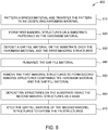
- Figure 8 illustrates a flow diagram of a method 800 for bottom up patterning and etching a substrate according to an embodiment described herein.
- the method 800 is discussed concurrently with the illustrations depicted in Figures 1-6 .
- a spacer material is patterned and the pattern is transferred to an underlying hardmask material.
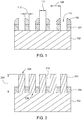
- Figure 1 illustrates a partial cross-sectional view of a substrate 102 having a patterned spacer material 106 and a hardmask material 104 formed thereon according to an embodiment described herein.
- the substrate 102 is fabricated from a semiconducting material, such as silicon.
- the substrate 102 is a monocrystalline silicon material which is either an intrinsic (un-doped) silicon material or an extrinsic (doped) silicon material. If an extrinsic silicon material is utilized, the dopant may be a p-type dopant, such as boron.
- the substrate 102 is a silicon-on-insulator substrate.
- the spacer material 106 and the hardmask material 104 are patterned. Prior to patterning, the hardmask material 104 is deposited on and in contact with the substrate 102 in a blanket type layer. The spacer material 106 is then deposited on and in contact with the hardmask material 104. Patterning of the spacer material 106 is performed by various processes suitable for advanced technology nodes, such as the 10 nm node, the 7 nm node, the 5 nm node, and beyond. Examples of suitable patterning processes include self-aligned double patterning and self-aligned quadruple patterning which are, depending upon the desired implementation, immersion lithography or extreme ultraviolet (EUV) lithography processes. Other suitable patterning processes include directed self-assembly, 193 nm immersion litho-etch-litho-etch (LELE), and EUV LELE, among others.
- LELE immersion litho-etch-litho-etch
- the patterned spacer material 106 creates a mask for subsequent etching of the underlying hardmask material 104.
- the spacer material 106 is a silicon oxide material, a silicon nitride material, or a titanium oxide material.
- a thickness of the patterned spacer material 106 is approximately equal to one half of the fin pitch.
- the thickness of the patterned spacer material is between about 15 nm and about 20 nm.
- a thickness of the hardmask material 104 is between about 30 nm and about 50 nm, such as about 40 nm.
- the hardmask material 104 is fabricated from a silicon oxide material in one embodiment and a silicon nitride material in another embodiment.
- An etching process such as a wet etching process or dry etching process, is utilized to etch the hardmask material 104, thus transferring the pattern from the spacer material 106 to the hardmask material.
- the etching process is a dry etching process.
- a nitride or oxide containing film is etched with a fluorine containing plasma generated from one or more of the following precursors: CF 4 , CHF 3 , CH 2 F 2 , CH 3 F, C 4 F 6 , or C 4 F 8 .
- a source power utilized to generate the plasma is between about 300W and about 1500W
- a bias power utilized to bias the plasma is between about 50 W and about 700W
- a pressure of a process environment for performing the etching process is maintained between about 5 mTorr and about 20 mTorr
- a temperature of the substrate 102 during the etching process is maintained between about 10°C and about 80°C.
- a pitch 108 of the patterned hardmask 106 is less than about 40 nm, such as about 30 nm or less.
- a width 110 of certain hardmask material portions is about 20 nm or less, such as about 15 nm or less.
- a width 112 of the exposed regions 114 is about 20 nm or less, such as about 15 nm or less.
- first mandrel structures 202 are formed on a substrate patterned by the hardmask material 104.
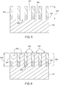
- Figure 2 illustrates a partial cross-sectional view of the substrate of Figure 1 with the spacer material 106 removed and first mandrel structures 202 formed on the substrate 102 according to an embodiment described herein.
- the spacer material 106 is removed by suitable selective etching processes, such as wet etching or drying etching processes.
- a plasma is generated from one or more of the following precursors: C 4 F 6 , O 2 , Ar, and He.
- a source power utilized to generate the plasma is between about 300W and about 900W
- a bias power utilized to bias the plasma is between about 300W and about 700W
- a pressure of a process environment for performing the etching process is maintained between about 5 mTorr and about 15 mTorr.
- a plasma is generated from one or more of the following precursors: CH 3 F, CH 4 , O 2 , H 2 , N 2 , and He.
- a source power utilized to generate the plasma is between about 400W and about 800W and a bias power utilized to bias the plasma is between about 30W and about 100W.
- a dilute HF wet etching process is utilized.
- suitable apparatus for performing the etching process is the CENTRISTM SYM3TM etching apparatus available from Applied Materials, Inc., Santa Clara, CA. It is contemplated that other suitably configured apparatus from other manufacturers may also be utilized in accordance with the embodiments described herein.
- the spacer removal process removes the spacer material 106 selectively to the hardmask material 104 and the substrate 102, leaving the hardmask material 104 on the substrate 102.
- the first mandrel structures 202 are formed in the exposed regions 114 depicted in Figure 1 .
- the first mandrel structures 202 are deposited on a surface 206 of the substrate and the first mandrel structures 202 grown from the surface 206 of the substrate 102.
- a suitable apparatus for performing the first mandrel structure deposition is the CENTURA® RP EPI apparatus available from Applied Materials, Inc., Santa Clara, CA. It is contemplated that other suitably configured apparatus from other manufacturers may also be utilized in accordance with the embodiments described herein.
- Each of the first mandrel structures 202 are separated from adjacent first mandrel structures 202 by the patterned hardmask material 104 and spaces 210.
- the first mandrel structures 202 are grown such that a top surface 208 of the first mandrel structures 202 is a distance 204 or greater than about 80 nm above the surface 206 of the substrate 102. In one embodiment, the distance 204 is between about 100 nm and about 200 nm.
- the first mandrel structures 202 are formed on the substrate 102 by an epitaxial deposition process.
- a gallium containing precursor and an arsenic containing precursor are pulsed in an alternating matter to deposit the first mandrel structures 202.
- the gallium containing precursor is trimethylgallium and the arsenic containing precursor is AsH 3 .
- the first mandrel structures 202 are fabricated in an environment maintained at a pressure of between about 1 Torr and about 10 Torr and a temperature of between about 450°C and about 800°C.
- the epitaxial deposition process utilizes a layer-by-layer deposition technique which is believed to maintain the substantially vertical orientation of the first mandrel structures 202 as the first mandrel structures 202 continue to grow from the surface 206 and above the hardmask material 104.
- the first mandrel structures 202 are formed from a III-V material.
- the first mandrel structures 202 are formed from one or more of aluminum antimonide, aluminum arsenide, aluminum gallium arsenide, aluminum gallium indium phosphide, aluminum gallium nitride, aluminum gallium phosphide, aluminum indium arsenide, aluminum nitride, aluminum phosphide, boron arsenide, boron nitride, boron phosphide, gallium antimonide, gallium arsenide, gallium arsenide phosphide, gallium phosphide, indium antimonide, indium arsenide, indium gallium arsenide, indium gallium nitride, indium gallium phosphide, indium nitride, and indium phosphide, among others.
- the gap fill material 302 is deposited on the substrate 102 over the hardmask material 104 and the first mandrel structures 202.
- Figure 3 illustrates a partial cross-sectional view of the substrate 102 of Figure 2 with a gap fill material 302 formed on the substrate 102 over the hardmask material 104 and the first mandrel structures 202 according to an embodiment described herein.
- the gap fill material 302 is deposited such that the gap fill material fills the voids 210 and is deposited to a thickness beyond the top surface 208 of the first mandrel structures 202.
- a suitable apparatus for performing the gap fill deposition process is the PRODUCER® ETERNATM FCVDTM apparatus available from Applied Materials, Inc., Santa Clara, CA. It is contemplated that suitably configured apparatus from other manufacturers may also be utilized in accordance with the embodiments described herein.
- the gap fill material is a flowable material.
- the flowable material has characteristics of a solid material but also has the ability to "flow," thus enabling substantially void-free bottom up material deposition.
- the gap fill material 302 is deposited by a flowable chemical vapor deposition (CVD) process.
- CVD chemical vapor deposition
- a CVD process is utilized to deposit a flowable silicon oxide containing gap fill material 302.
- a silicon oxide material is sequentially deposited, cured, and annealed.
- a CVD process is utilized to deposit a silicon nitride gap fill material 302.
- a silicon nitride material is sequentially deposited and subjected to a nitridation plasma treatment.
- the gap fill material 302 is formed by a spin on glass (SOG) process.
- the gap fill material 302 is an oxide containing material, such as silicon dioxide or the like.
- the gap fill material is planarized.
- Figure 4 illustrates a partial cross-sectional view of the substrate 102 of Figure 3 after planarization of the gap fill material 302 according to an embodiment described herein.
- planarization of the gap fill material 302 is performed by a chemical mechanical polishing process.
- planarization of the gap fill material 302 is performed by an etching process.
- the gap fill material 302 is removed to a point where a top surface 402 of the gap fill material 302 is substantially planar with the top surface 208 of the first mandrel structures 202. In one embodiment, it is contemplated that the first mandrel structures 202 are utilized as a removal point. In another embodiment, the gap fill material 302 is subjected to a time based etching process to planarize the surfaces 402, 208.
- the first mandrel structures 202 are removed to form the second mandrel structures 500 which include the hardmask material 104 and the gap fill material 302.
- Figure 5 illustrates a partial cross-sectional view of the substrate 102 of Figure 4 with the first mandrel structures 202 removed to form second mandrel structures 500 according to an embodiment described herein.
- a selective etching process is utilized to remove the first mandrel structures 202.
- etch chemistries selective to III-V materials are utilized to remove the first mandrel structures 202 selectively to the oxide and/or nitride containing gap fill material 302 and hardmask material 104.
- a chlorine containing precursor such as HCI
- HCI is delivered to a process environment with a hydrogen containing precursor, such as H 2 .
- the precursors are delivered to the process environment with an inert carrier gas such as N 2 or Ar.
- the HCI is delivered to the process environment at a flow rate of between about 1 sccm and about 500 sccm.
- a temperature of the process environment is maintained between about 300°C and about 700°C and a pressure of the process environment is maintained between about 0 Torr and about 100 Torr.
- Removal of the first mandrel structures 202 results in spaces 502 formed between adjacent second mandrel structures 500.
- the spaces 502 also expose a second region of the top surface 206 of the substrate 102.
- a height 504 of the second mandrel structures 500 is similar to the distance 204, for example, substantially equal to the distance 204.
- the fin structures 602 are deposited on the substrate 102 using the second mandrel structures 500 as a mask.
- Figure 6 illustrates a partial cross-sectional view of the substrate 102 of Figure 5 after forming fin structures 602 on the substrate 102 according to an embodiment described herein.
- the fin structures 602 extend a second distance 606 of greater than about 80 nm, such as between about 100 nm and about 200 nm, above the surface 206.
- the fin structures 602 are formed by an epitaxial deposition process.
- the material utilized to form the fin structures 602 are the same as the material utilized to form the substrate 102.
- the materials utilized to form the fin structures include silicon containing materials, germanium containing materials, silicon germanium containing material, and III-V materials, among others.
- a dichlorosilane precursor and a GeH 4 precursor are activated and pulsed in an alternating manner to deposit a silicon germanium material as the fin structures 602.
- the fin structures 602 extend the second distance 606 such that a top surface 604 of the fin structures 602 are substantially co-planar with the top surface 402 of the gap fill material 302.
- the fin structures 602 exhibit improved verticality profile due to the improved verticality of the hardmask material 104 and the gap fill material 302 of the second mandrel structures 500.
- the second mandrel structures 500 are also believed to reduce lateral growth of the fin structures 602 during formation and may also reduce undesirable facet formation within the fin structures 602.
- the gap fill material 302 of the second mandrel structures 500 is etched to expose the fin structures 602.
- Figure 7 illustrates a partial cross-sectional view of the substrate 102 of Figure 6 after etching the gap fill material 302 according to an embodiment described herein.
- the top surface 402 of the gap fill material 302 is recessed from the top surface 604 of the fin structures a third distance 704 of greater than about 80 nm, such as between about 100 nm and about 200 nm.
- the gap fill material 302 is etched by a selective etching process that preferentially etches to the oxide or nitride materials of the gap fill material 302.
- a SICONI® process available from Applied Materials, Inc., Santa Clara, CA, is utilized to etch the gap fill material 302.
- second mandrel structures 500 may remain disposed on the substrate 102 to provide for fin isolation or may be removed, depending upon the desired device implementation.
- improved mask formation and etching process flows provide for bottom up fin formation for the fabrication of advanced semiconductor devices.
- improved etching verticality may be achieved.
- sidewall verticality of the masks first and second mandrel structures
- sidewall (lateral growth) is more effectively controlled and edge roughness is also reduced.
Landscapes
- Insulated Gate Type Field-Effect Transistor (AREA)
- Thin Film Transistor (AREA)
- Semiconductor Memories (AREA)
- Drying Of Semiconductors (AREA)
Applications Claiming Priority (1)
| Application Number | Priority Date | Filing Date | Title |
|---|---|---|---|
| US15/896,839 US10204781B1 (en) | 2018-02-14 | 2018-02-14 | Methods for bottom up fin structure formation |
Publications (2)
| Publication Number | Publication Date |
|---|---|
| EP3528290A2 true EP3528290A2 (de) | 2019-08-21 |
| EP3528290A3 EP3528290A3 (de) | 2019-12-18 |
Family
ID=65241821
Family Applications (1)
| Application Number | Title | Priority Date | Filing Date |
|---|---|---|---|
| EP19156890.6A Withdrawn EP3528290A3 (de) | 2018-02-14 | 2019-02-13 | Verfahren zur rippenstrukturbildung von unten nach oben |
Country Status (6)
| Country | Link |
|---|---|
| US (2) | US10204781B1 (de) |
| EP (1) | EP3528290A3 (de) |
| JP (1) | JP2019140395A (de) |
| KR (1) | KR20190098715A (de) |
| CN (1) | CN110164973A (de) |
| TW (1) | TW201935527A (de) |
Families Citing this family (6)
| Publication number | Priority date | Publication date | Assignee | Title |
|---|---|---|---|---|
| US10204781B1 (en) * | 2018-02-14 | 2019-02-12 | Applied Materials, Inc. | Methods for bottom up fin structure formation |
| US11239368B2 (en) * | 2019-08-30 | 2022-02-01 | Taiwan Semiconductor Manufacturing Company, Ltd. | Semiconductor device and method |
| US11482411B2 (en) * | 2020-06-30 | 2022-10-25 | Taiwan Semiconductor Manufacturing Co., Ltd. | Semiconductor device and method |
| US11462406B2 (en) * | 2020-07-29 | 2022-10-04 | Nanya Technology Corporation | Semiconductor device structure with fine boron nitride spacer patterns and method for forming the same |
| US12374584B2 (en) | 2020-10-28 | 2025-07-29 | Applied Materials, Inc. | Multi color stack for self aligned dual pattern formation for multi purpose device structures |
| US20250176158A1 (en) * | 2023-11-24 | 2025-05-29 | Nanya Technology Corporation | Assembly structure including a plurality of spacers and method of manufacturing the same |
Family Cites Families (25)
| Publication number | Priority date | Publication date | Assignee | Title |
|---|---|---|---|---|
| JP3540633B2 (ja) | 1998-11-11 | 2004-07-07 | 株式会社東芝 | 半導体装置の製造方法 |
| US6864164B1 (en) | 2002-12-17 | 2005-03-08 | Advanced Micro Devices, Inc. | Finfet gate formation using reverse trim of dummy gate |
| US6855582B1 (en) | 2003-06-12 | 2005-02-15 | Advanced Micro Devices, Inc. | FinFET gate formation using reverse trim and oxide polish |
| US7018551B2 (en) | 2003-12-09 | 2006-03-28 | International Business Machines Corporation | Pull-back method of forming fins in FinFets |
| US7470570B2 (en) | 2006-11-14 | 2008-12-30 | International Business Machines Corporation | Process for fabrication of FinFETs |
| US7772048B2 (en) | 2007-02-23 | 2010-08-10 | Freescale Semiconductor, Inc. | Forming semiconductor fins using a sacrificial fin |
| JP5731858B2 (ja) | 2011-03-09 | 2015-06-10 | ピーエスフォー ルクスコ エスエイアールエルPS4 Luxco S.a.r.l. | 半導体装置及び半導体装置の製造方法 |
| US8637359B2 (en) | 2011-06-10 | 2014-01-28 | International Business Machines Corporation | Fin-last replacement metal gate FinFET process |
| US8669186B2 (en) | 2012-01-26 | 2014-03-11 | Globalfoundries Inc. | Methods of forming SRAM devices using sidewall image transfer techniques |
| CN103855009B (zh) | 2012-11-30 | 2017-06-13 | 中国科学院微电子研究所 | 鳍结构制造方法 |
| US8828839B2 (en) | 2013-01-29 | 2014-09-09 | GlobalFoundries, Inc. | Methods for fabricating electrically-isolated finFET semiconductor devices |
| US8975155B2 (en) * | 2013-07-10 | 2015-03-10 | Taiwan Semiconductor Manufacturing Company, Ltd. | Method of forming a shallow trench isolation structure |
| CN104347421A (zh) | 2013-08-07 | 2015-02-11 | 中芯国际集成电路制造(北京)有限公司 | 鳍式场效应管的形成方法 |
| US9564361B2 (en) | 2013-09-13 | 2017-02-07 | Qualcomm Incorporated | Reverse self aligned double patterning process for back end of line fabrication of a semiconductor device |
| US9245882B2 (en) | 2013-09-27 | 2016-01-26 | Taiwan Semiconductor Manufacturing Company, Ltd. | FinFETs with gradient germanium-containing channels |
| US8993419B1 (en) | 2013-10-03 | 2015-03-31 | Applied Materials, Inc. | Trench formation with CD less than 10 NM for replacement Fin growth |
| US9023705B1 (en) | 2013-11-01 | 2015-05-05 | Globalfoundries Inc. | Methods of forming stressed multilayer FinFET devices with alternative channel materials |
| US9412603B2 (en) | 2013-11-19 | 2016-08-09 | Applied Materials, Inc. | Trimming silicon fin width through oxidation and etch |
| US9224654B2 (en) | 2013-11-25 | 2015-12-29 | International Business Machines Corporation | Fin capacitor employing sidewall image transfer |
| US20150187909A1 (en) * | 2013-12-30 | 2015-07-02 | Global Foundries, Inc. | Methods for fabricating multiple-gate integrated circuits |
| US9252208B1 (en) | 2014-07-31 | 2016-02-02 | Stmicroelectronics, Inc. | Uniaxially-strained FD-SOI finFET |
| US9209279B1 (en) | 2014-09-12 | 2015-12-08 | Applied Materials, Inc. | Self aligned replacement fin formation |
| US9530637B2 (en) | 2014-10-05 | 2016-12-27 | Applied Materials, Inc. | Fin structure formation by selective etching |
| US10096524B1 (en) * | 2017-10-18 | 2018-10-09 | International Business Machines Corporation | Semiconductor fin patterning techniques to achieve uniform fin profiles for fin field effect transistors |
| US10204781B1 (en) * | 2018-02-14 | 2019-02-12 | Applied Materials, Inc. | Methods for bottom up fin structure formation |
-
2018
- 2018-02-14 US US15/896,839 patent/US10204781B1/en active Active
-
2019
- 2019-01-28 US US16/259,585 patent/US10741393B2/en not_active Expired - Fee Related
- 2019-02-12 TW TW108104540A patent/TW201935527A/zh unknown
- 2019-02-13 CN CN201910116287.7A patent/CN110164973A/zh active Pending
- 2019-02-13 KR KR1020190016593A patent/KR20190098715A/ko not_active Withdrawn
- 2019-02-13 EP EP19156890.6A patent/EP3528290A3/de not_active Withdrawn
- 2019-02-14 JP JP2019024076A patent/JP2019140395A/ja active Pending
Non-Patent Citations (1)
| Title |
|---|
| None |
Also Published As
| Publication number | Publication date |
|---|---|
| TW201935527A (zh) | 2019-09-01 |
| KR20190098715A (ko) | 2019-08-22 |
| US10204781B1 (en) | 2019-02-12 |
| CN110164973A (zh) | 2019-08-23 |
| EP3528290A3 (de) | 2019-12-18 |
| JP2019140395A (ja) | 2019-08-22 |
| US20190252187A1 (en) | 2019-08-15 |
| US10741393B2 (en) | 2020-08-11 |
Similar Documents
| Publication | Publication Date | Title |
|---|---|---|
| US9373546B2 (en) | Self aligned replacement Fin formation | |
| US10741393B2 (en) | Methods for bottom up fin structure formation | |
| US12408367B2 (en) | Semiconductor device | |
| US9530637B2 (en) | Fin structure formation by selective etching | |
| US11164940B2 (en) | Method of forming III-V on insulator structure on semiconductor substrate | |
| US12002683B2 (en) | Lateral etching of silicon | |
| US12087847B2 (en) | Variable size fin structures | |
| US10439047B2 (en) | Methods for etch mask and fin structure formation | |
| CN108987476B (zh) | 半导体结构及其形成方法 | |
| CN106531631B (zh) | 一种形成鳍的方法及结构 |
Legal Events
| Date | Code | Title | Description |
|---|---|---|---|
| PUAI | Public reference made under article 153(3) epc to a published international application that has entered the european phase |
Free format text: ORIGINAL CODE: 0009012 |
|
| STAA | Information on the status of an ep patent application or granted ep patent |
Free format text: STATUS: THE APPLICATION HAS BEEN PUBLISHED |
|
| AK | Designated contracting states |
Kind code of ref document: A2 Designated state(s): AL AT BE BG CH CY CZ DE DK EE ES FI FR GB GR HR HU IE IS IT LI LT LU LV MC MK MT NL NO PL PT RO RS SE SI SK SM TR |
|
| AX | Request for extension of the european patent |
Extension state: BA ME |
|
| PUAL | Search report despatched |
Free format text: ORIGINAL CODE: 0009013 |
|
| AK | Designated contracting states |
Kind code of ref document: A3 Designated state(s): AL AT BE BG CH CY CZ DE DK EE ES FI FR GB GR HR HU IE IS IT LI LT LU LV MC MK MT NL NO PL PT RO RS SE SI SK SM TR |
|
| AX | Request for extension of the european patent |
Extension state: BA ME |
|
| RIC1 | Information provided on ipc code assigned before grant |
Ipc: H01L 29/66 20060101AFI20191108BHEP Ipc: H01L 21/308 20060101ALN20191108BHEP Ipc: H01L 29/78 20060101ALN20191108BHEP |
|
| STAA | Information on the status of an ep patent application or granted ep patent |
Free format text: STATUS: REQUEST FOR EXAMINATION WAS MADE |
|
| 17P | Request for examination filed |
Effective date: 20200618 |
|
| RBV | Designated contracting states (corrected) |
Designated state(s): AL AT BE BG CH CY CZ DE DK EE ES FI FR GB GR HR HU IE IS IT LI LT LU LV MC MK MT NL NO PL PT RO RS SE SI SK SM TR |
|
| STAA | Information on the status of an ep patent application or granted ep patent |
Free format text: STATUS: THE APPLICATION IS DEEMED TO BE WITHDRAWN |
|
| 18D | Application deemed to be withdrawn |
Effective date: 20210901 |