EP3528237A1 - Current correction techniques for accurate high current short channel driver - Google Patents
Current correction techniques for accurate high current short channel driver Download PDFInfo
- Publication number
- EP3528237A1 EP3528237A1 EP19157716.2A EP19157716A EP3528237A1 EP 3528237 A1 EP3528237 A1 EP 3528237A1 EP 19157716 A EP19157716 A EP 19157716A EP 3528237 A1 EP3528237 A1 EP 3528237A1
- Authority
- EP
- European Patent Office
- Prior art keywords
- current
- output
- node
- terminal
- voltage
- Prior art date
- Legal status (The legal status is an assumption and is not a legal conclusion. Google has not performed a legal analysis and makes no representation as to the accuracy of the status listed.)
- Granted
Links
Images



Classifications
-
- G—PHYSICS
- G05—CONTROLLING; REGULATING
- G05F—SYSTEMS FOR REGULATING ELECTRIC OR MAGNETIC VARIABLES
- G05F3/00—Non-retroactive systems for regulating electric variables by using an uncontrolled element, or an uncontrolled combination of elements, such element or such combination having self-regulating properties
- G05F3/02—Regulating voltage or current
- G05F3/08—Regulating voltage or current wherein the variable is DC
- G05F3/10—Regulating voltage or current wherein the variable is DC using uncontrolled devices with non-linear characteristics
- G05F3/16—Regulating voltage or current wherein the variable is DC using uncontrolled devices with non-linear characteristics being semiconductor devices
- G05F3/20—Regulating voltage or current wherein the variable is DC using uncontrolled devices with non-linear characteristics being semiconductor devices using diode- transistor combinations
- G05F3/24—Regulating voltage or current wherein the variable is DC using uncontrolled devices with non-linear characteristics being semiconductor devices using diode- transistor combinations wherein the transistors are of the field-effect type only
-
- H—ELECTRICITY
- H05—ELECTRIC TECHNIQUES NOT OTHERWISE PROVIDED FOR
- H05B—ELECTRIC HEATING; ELECTRIC LIGHT SOURCES NOT OTHERWISE PROVIDED FOR; CIRCUIT ARRANGEMENTS FOR ELECTRIC LIGHT SOURCES, IN GENERAL
- H05B45/00—Circuit arrangements for operating light-emitting diodes [LED]
- H05B45/30—Driver circuits
-
- G—PHYSICS
- G05—CONTROLLING; REGULATING
- G05F—SYSTEMS FOR REGULATING ELECTRIC OR MAGNETIC VARIABLES
- G05F3/00—Non-retroactive systems for regulating electric variables by using an uncontrolled element, or an uncontrolled combination of elements, such element or such combination having self-regulating properties
- G05F3/02—Regulating voltage or current
- G05F3/08—Regulating voltage or current wherein the variable is DC
- G05F3/10—Regulating voltage or current wherein the variable is DC using uncontrolled devices with non-linear characteristics
- G05F3/16—Regulating voltage or current wherein the variable is DC using uncontrolled devices with non-linear characteristics being semiconductor devices
- G05F3/20—Regulating voltage or current wherein the variable is DC using uncontrolled devices with non-linear characteristics being semiconductor devices using diode- transistor combinations
- G05F3/26—Current mirrors
- G05F3/262—Current mirrors using field-effect transistors only
-
- G—PHYSICS
- G09—EDUCATION; CRYPTOGRAPHY; DISPLAY; ADVERTISING; SEALS
- G09G—ARRANGEMENTS OR CIRCUITS FOR CONTROL OF INDICATING DEVICES USING STATIC MEANS TO PRESENT VARIABLE INFORMATION
- G09G3/00—Control arrangements or circuits, of interest only in connection with visual indicators other than cathode-ray tubes
- G09G3/04—Control arrangements or circuits, of interest only in connection with visual indicators other than cathode-ray tubes for presentation of a single character by selection from a plurality of characters, or by composing the character by combination of individual elements, e.g. segments using a combination of such display devices for composing words, rows or the like, in a frame with fixed character positions
- G09G3/06—Control arrangements or circuits, of interest only in connection with visual indicators other than cathode-ray tubes for presentation of a single character by selection from a plurality of characters, or by composing the character by combination of individual elements, e.g. segments using a combination of such display devices for composing words, rows or the like, in a frame with fixed character positions using controlled light sources
- G09G3/12—Control arrangements or circuits, of interest only in connection with visual indicators other than cathode-ray tubes for presentation of a single character by selection from a plurality of characters, or by composing the character by combination of individual elements, e.g. segments using a combination of such display devices for composing words, rows or the like, in a frame with fixed character positions using controlled light sources using electroluminescent elements
- G09G3/14—Semiconductor devices, e.g. diodes
-
- H—ELECTRICITY
- H05—ELECTRIC TECHNIQUES NOT OTHERWISE PROVIDED FOR
- H05B—ELECTRIC HEATING; ELECTRIC LIGHT SOURCES NOT OTHERWISE PROVIDED FOR; CIRCUIT ARRANGEMENTS FOR ELECTRIC LIGHT SOURCES, IN GENERAL
- H05B45/00—Circuit arrangements for operating light-emitting diodes [LED]
- H05B45/10—Controlling the intensity of the light
-
- H—ELECTRICITY
- H05—ELECTRIC TECHNIQUES NOT OTHERWISE PROVIDED FOR
- H05B—ELECTRIC HEATING; ELECTRIC LIGHT SOURCES NOT OTHERWISE PROVIDED FOR; CIRCUIT ARRANGEMENTS FOR ELECTRIC LIGHT SOURCES, IN GENERAL
- H05B45/00—Circuit arrangements for operating light-emitting diodes [LED]
- H05B45/30—Driver circuits
- H05B45/345—Current stabilisation; Maintaining constant current
-
- H—ELECTRICITY
- H05—ELECTRIC TECHNIQUES NOT OTHERWISE PROVIDED FOR
- H05B—ELECTRIC HEATING; ELECTRIC LIGHT SOURCES NOT OTHERWISE PROVIDED FOR; CIRCUIT ARRANGEMENTS FOR ELECTRIC LIGHT SOURCES, IN GENERAL
- H05B45/00—Circuit arrangements for operating light-emitting diodes [LED]
- H05B45/30—Driver circuits
- H05B45/395—Linear regulators
- H05B45/397—Current mirror circuits
-
- Y—GENERAL TAGGING OF NEW TECHNOLOGICAL DEVELOPMENTS; GENERAL TAGGING OF CROSS-SECTIONAL TECHNOLOGIES SPANNING OVER SEVERAL SECTIONS OF THE IPC; TECHNICAL SUBJECTS COVERED BY FORMER USPC CROSS-REFERENCE ART COLLECTIONS [XRACs] AND DIGESTS
- Y02—TECHNOLOGIES OR APPLICATIONS FOR MITIGATION OR ADAPTATION AGAINST CLIMATE CHANGE
- Y02B—CLIMATE CHANGE MITIGATION TECHNOLOGIES RELATED TO BUILDINGS, e.g. HOUSING, HOUSE APPLIANCES OR RELATED END-USER APPLICATIONS
- Y02B20/00—Energy efficient lighting technologies, e.g. halogen lamps or gas discharge lamps
- Y02B20/30—Semiconductor lamps, e.g. solid state lamps [SSL] light emitting diodes [LED] or organic LED [OLED]
Definitions
- the present disclosure relates generally to current driver circuitry, and more particularly to controlling current flow in current driver applications.
- a current driver is employed to control current flow through a diode, such as a Light Emitting Diode (LED).
- a remote control includes a microcontroller, the current driver, the LED, and a battery that supplies a Direct Current (DC) voltage onto a supply node.
- One terminal of the LED is coupled to the supply node and another terminal of the LED is coupled in some fashion to the current driver.
- the current driver controls an output current that flows through the LED, either by sourcing current from the battery, through the current driver, through the LED and onto a ground node, or by sinking current from the supply node, through the LED, through the current driver, and onto the ground node.
- the current driver uses a reference current to set a current level of the output current through the LED. The current level of the output current is generally desired to be maintained at a pre- determined multiple of the reference current.
- a system comprises a supply node, a controller integrated circuit (IC), a current driver IC, a diode, and a ground node.
- the current driver IC is an example of a high current driver that controls currents greater than at least 200 milliamps through the diode.
- the diode is a Light Emitting Diode (LED) and the current driver IC is coupled to sink current from the supply node, through the diode, through the current driver IC, and onto the ground node.
- the LED has an anode coupled to a supply node and a cathode coupled to a drive terminal of the current driver IC.
- the current driver has a control terminal coupled to receive a control signal EN from the controller IC that enables (turning on the LED) ordisables (turning off the LED) the current driver IC.
- the supply node is supplied by Direct Current (DC) source such as a battery.
- the supply node is supplied by an Alternating Current (AC) source, such as an AC line.
- DC Direct Current
- AC Alternating Current
- the current driver IC is enabled and sinks an output current from the supply node, through the LED, through the drive terminal, and onto a ground node.
- An output voltage is present between the cathode of the LED and the ground node.
- the output voltage typically varies due to charge and discharge cycles of the battery which cause the battery voltage to decrease over time.
- the output voltage may also vary depending on the voltage and current demands across different applications.
- changes in temperature of the LED may also cause the output voltage to change.
- the current driver IC maintains variation of a current level of the output current to be within five percent of a desired output current level when the output voltage is anywhere within at least a two-volt range.
- the desired output current level is 250 milliamps
- the current driver IC controls the output current to be between 255 milliamps and 245 milliamps when the output voltage is anywhere between at least 0.3 volts and 2.4 volts.
- the current driver integrated circuit comprises a voltage detector circuit, an Output Model Current Mirror (OMCM) circuit, a Corrected Current Mirror (CCM) circuit, a summing node reference current generator circuit, a Corrected Current to Gate Voltage Converter (CCGVC) circuit, a summing node, and a current drive transistor.
- the voltage detector circuit detects an output voltage on an output node and generates a replica voltage.
- the OMCM circuit receives the replica voltage and generates an output model current I s .
- the output model current I S models a short channel effect on the current driver transistor.
- the output model current I S is a factor of the reference current I REF modulated by the output voltage V OUT . In this example, the factor is approximately one.
- the short channel current modulation is caused by short channel effects present on a transistor of the OMCM circuit that is coupled to detect the replica voltage.
- the transistor of the OMCM circuit that detects the replica voltage has a drain terminal on which the replica voltage is present.
- the amount of modulation is adjustable by adjusting the length of the transistor that detects the replica voltage. The length of this transistor is adjusted to increase or decrease the amount of short channel current modulation to match that of the current driver transistor.
- the summing node is maintained at a stable current level which is a first factor times a reference current.
- a current on the summing node is maintained to be twice a reference current ("2xI REF ").
- the OMCM circuit supplies the output model current I s onto the summing node, and the CCM circuit generates and supplies a corrected current I C onto the summing node. Because the current on the summing node is substantially constant, and because both the output model current I S and the corrected current I C are supplied onto the summing node, as the output model current I S decreases, the corrected current I C increases.
- a scaled corrected current I D is used to generate a gate voltage that controls operation of the current driver transistor.
- the CCM circuit generates the scaled corrected current I D by scaling the corrected current I C by a second factor. For example, the scaled corrected current I D is fifteen times the corrected current I C .
- the CCGVC circuit receives the scaled corrected current I D and converts the scaled corrected current I D into a gate voltage.
- the CCGVC circuit supplies the gate voltage onto a gate terminal of the current driver transistor.
- the gate voltage controls the conductivity of the current driver transistor such that current flow through the diode remains within five percent of the desired output current level over at least a 2V range of the output voltage.
- the desired output current level is a third factor times the scaled corrected current I D .
- the current level of the output current I OUT is two-hundred and six times the scaled corrected current I D .
- the increase in corrected current I C compensates for the decrease in output model current due to variation in the output voltage V OUT thereby controlling the current level of the output current I OUT to be maintained within five percent of the desired output current level.
- Figure 1 is a circuit diagram of a current driver circuit 10 having a single drive transistor 11.
- the current driver circuit 10 includes a reference current generator 12 and a current mirror circuit 13.
- the current mirror circuit includes the drive field effect transistor 11 and field effect transistor 14.
- a gate terminal of transistor 14 is coupled to a drain terminal of the transistor 14.
- the gate terminal of transistor 14 is also coupled to a gate terminal of the drive transistor 11.
- the drive transistor 11 is approximately two-hundred ("200") times the size of transistor 14.
- the current driver circuit 10 drives load 15 from supply node 16.
- a load 15 is coupled between a supply node 16 and a drain terminal of the drive transistor 11.
- a source terminal of the drive transistor 11 is coupled to a ground node 17.
- the current driver circuit 10 drives the load 15 by sinking current I OUT 18 from a supply node 16 through the load 15 through the drive field effect transistor 11 and onto a ground node 17.
- the reference current generator circuit 12 outputs a reference current I REF 19 onto a drain terminal of the transistor 14.
- the output current I OUT 18 that flows through the load 15 is a factor of the reference current I REF 19.
- the factor is determined by a ratio of the size of the drive transistor 11 to the size of the transistor 14. In this example, the factor is two-hundred ("200") because the drive transistor 11 is approximately two-hundred ("200") times the size of transistor 14.
- the output current I OUT 18 will be 200 times the reference current I REF 19.
- the reference current I REF 19 is approximately 1.2 milliamps and the output current I OUT 18 will be approximately 240 milliamps.
- the output current I OUT 18 In most applications of current driver circuit 10, it is desirable for the output current I OUT 18 to remain constant and at a fixed factor of the reference current I REF 19 across a range of output voltage V OUT 20. However, during operation of the current driver circuit 10, the output current I OUT 18 tends to change as the output voltage V OUT 20 changes. As shown in Figure 3 , the output current I OUT 18 varies approximately 90 milliamps over a 2V range of output voltage 20.
- FIG 2 is a diagram of a top-down view of drive transistor 11 shown in Figure 1 .
- the drive transistor 11 includes a polysilicon gate 21, a drain region 22, and a source region 23.
- the variation of the output current I OUT 18 can be minimized by increasing length L of the polysilicon gate 21.
- increasing the length L requires increasing the width W to maintain the same width to length ratio of the drive transistor 11, which in turn, increases the overall size of drive transistor 11.
- Increasing the size of drive transistor 11 is generally undesirable due to increased die area that would be consumed by the drive transistor 11. For example, if the width W increases by a factor of two ("2”), then the length L would also be increased by a factor of two (“2”) to maintain the width to length ratio.
- an overall die area of the transistor would increase by a factor of four ("4").
- FIG 3 is a diagram showing graphs of the output current I out 18 and reference current I REF 19 versus the output voltage V out 20 during operation of the current driver circuit 10 shown in Figure 1 .
- the output voltage V out 20 extends approximately 2V ranging from 0.4 V to 2.4V.
- the reference current I REF 19 is set at a constant 1.2 milliamps over the range of output voltages.
- the output current extends from around 185 milliamps to approximately 275 milliamps over the range of output voltages.
- the current driver circuit 10 shown in Figure 1 has an output current 18 that varies approximately 90 milliamps over a 2.0V range of output voltages. As identified by dashed line 24, when the output voltage V out 20 is less than 0.6V, the output current I out 18 increases much more rapidly as compared to when the output voltage V OUT 20 is greaterthan 0.6 V.
- FIG. 4 is a circuit diagram of a current driver circuit 30 having two high power output transistors 31 and 32.
- Current driver circuit 30 comprises a reference current generator 33, the drive transistor 31, and the cascode transistor 32.
- a drain terminal of the cascode transistor 32 is coupled to load 35.
- a source terminal of the cascode transistor 32 is coupled to a drain terminal of the drive transistor 31.
- the current driver circuit 30 sinks an output current I OUT 36 from the supply node 37, through load 35, through cascode transistor 32, through drive transistor 31, and onto a ground node 38.
- the reference current generator 33 outputs a reference current I REF 39 onto a drain terminal of the transistor 34.
- the output current I OUT 36 is a factor of the reference current I REF 39.
- the factor depends upon a width to length ratio of the drive transistor 31 and a width to length ratio of transistor 34.
- An output voltage V OUT 40 is present between a drain terminal of the cascode transistor 32 and a source terminal of the drive transistor 31.
- the cascode transistor 32 and the drive transistor 31 are each two-hundred ("200") times a sizeof the transistor 34.
- Figure 5 is a diagram showing graphs of the output current I OUT 36 and reference current I REF 39 versus the output voltage V out 40 during operation of the current driver circuit 30 shown in Figure 4 .
- the output current I OUT 36 tends to vary depending on the output voltage V OUT 40. As identified by dashed line 41, when the output voltage V out 40 is less than 0.8V, the output current I out 36 increases much more rapidly as compared to when the output voltage V OUT 40 is greater than 0.8 V. Over a range of 2V of the output voltage V OUT 40, the current I OUT 36 of the current driver circuit 30 varies by approximately 100 milliamps.
- FIG. 6 is a circuit diagram of system 50 involving a novel current driver integrated circuit 51.
- System 50 comprises the current driver integrated circuit 51, a battery 52, a controller integrated circuit 53, a diode 54, a supply node 55, and a ground node 56.
- the battery 52 has a positive terminal that is coupled to the supply node 55, and a negative terminal that is coupled to the ground node 56.
- the battery 52 controls the supply node 55 to be at a fixed voltage VDD.
- VDD is between 2.7 V and 3.3 V.
- diode 54 is a light emitting diode (LED).
- system 50 is part of a remote control in which current is pulsed through the diode thereby radiating energy used in wireless communication.
- the controller integrated circuit 53 has a supply terminal 57, a control terminal 58, and a ground terminal 59.
- the supply terminal 57 of the controller integrated circuit 53 is coupled to the supply node 55.
- the ground terminal 59 of the controller integrated circuit 53 is coupled to the ground node 56.
- the current driver integrated circuit 51 has a supply terminal 60, a control terminal 61, a drive terminal 62, and a ground terminal 63.
- the supply terminal 60 of the current driver integrated circuit 51 is coupled to the supply node 55.
- the ground terminal 63 of the current driver integrated circuit 51 is coupled to the ground node 56.
- the control terminal 61 of the current driver integrated circuit 51 is coupled to the control terminal 58 of the controller integrated circuit 53.
- the current driver IC 51 is an integrated circuit die and the terminals 60-63 are bond pads.
- Diode 54 has an anode terminal A that is coupled to the supply node 55.
- Diode 54 has a cathode terminal C that is coupled to the drive terminal 62 of the current driver integrated circuit 51.
- the controller integrated circuit 53 and current driver integrated circuit 51 are supplied by a direct current (DC) source, however, in other embodiments the controller integrated circuit 53 and the current driver integrated circuit 51 are supplied from an Alternating Current (AC) source.
- DC direct current
- AC Alternating Current
- the diode 54 is initially off and in a non-conductive state such that no current is flowing through diode 54.
- the controller integrated circuit 53 determines that the diode 54 is to switch from a non-conductive state to a conductive state such that current is to flow through the diode 54.
- Controller integrated circuit 53 asserts a control signal EN 64 that is supplied from the control terminal 58 onto the control terminal 61 of the current driver integrated circuit 51 via conductor 64.
- the current driver integrated circuit 51 sinks current from the supply node 55 through the diode 66, and onto the ground node 56 through the current driver integrated circuit 51.
- the current driver integrated circuit 51 drives the diode 54 such that the output current I OUT 66 varies by less than 10% over a range of output voltage V OUT 67.
- the battery voltage might start out at 3.6V and a typical voltage drop across the LED might be 1.2V, so the output voltage V OUT 67 would be 2.4V. If the battery discharges to 1.8V, then the output voltage V OUT 67 could decrease to 0.6V.
- the output current I OUT 66 remains within a desired output current range where the output voltage V OUT 67 ranges between 0.4V and 2.4V (or a 2V range).
- the current driver integrated circuit 51 drives the diode 54 such that the output current I OUT 66 varies by less than four percent over at least a two-volt range of output voltages V OUT 67. In another example, the current driver integrated circuit 51 drives the diode 54 such that the output current I OUT 66 varies by less than ten percent over at least a two-volt range of output voltages V OUT 67.
- FIG. 7 is a detailed circuit diagram of the current driver integrated circuit 51 shown in Figure 6 .
- the current driver integrated circuit 51 comprises voltage detector circuit 70, an Output Model Current Mirror (OMCM) circuit 71, a Corrected Current Mirror (CCM) circuit 72, a summing node reference current generator circuit 73, a Corrected Current To Gate Voltage Converter (CCGVC) circuit 74, a reference current generator 75, a bias current generator 76, a current drive transistor 77, an inverter 78, transistors 79, 80, 81 and 82, a replica node 83, an output node 84, a reference current node 85, a bias current node 86, and a summing node 87.
- the reference current generator 75 generates and outputs a reference current I REF 88 onto the reference current node 85.
- the bias current generator 76 generates and outputs a bias current I BIAS 89 on to the bias current node 86.
- the voltage detector circuit 70 detects the output voltage V OUT 67 on the output node 84 and generates a replica voltage 90.
- the voltage detector circuit 70 outputs the generated replica voltage 90 onto the replica node 83.
- the voltage detector circuit 70 comprises a first transistor 91 and a second transistor 92.
- a drain terminal and a gate terminal of first transistor 91 are coupled to the bias current node 86 and receives the bias current I BIAS 89.
- a source terminal of the first transistor 91 is coupled to the output node 84.
- a gate of the first transistor 91 is coupled to a gate of the second transistor 92.
- the detected output voltage V OUT 67 plus the voltage required to turn on the first transistor 91 is received onto the gate of the second transistor 92.
- a drain terminal of the second transistor 92 is coupled to the OMCM circuit 71 and a source terminal of the second transistor 92 is coupled to the replica node 83.
- the Output Model Current Mirror (OMCM) circuit 71 receives the replica voltage 90 generated by the voltage detector circuit 70 and generates an output model current I s 93.
- the output model current I S 93 is supplied onto the summing node 87.
- the output model current I S 93 is also referred to as a model short channel effect current because it models a short channel effect on the current driver transistor 77.
- the OMCM circuit 71 outputs the generated output model current I S 93 onto the summingnode 87.
- the output model current I S 93 is a factor of the I REF current88 modulated by the output voltage V OUT 67. In this example, the factor is approximately one.
- the short channel current modulation is due to short channel effects present on transistor 94. The amount of modulation is adjusted by adjusting the length of transistor 94 to increase or decrease the amount of short channel current modulation to match that of current driver transistor 77.
- the OMCM circuit 71 comprises a first transistor 94, second transistor 95, and a third transistor 96.
- the second transistor 95 and the third transistor 96 form a current mirror.
- the gate of the second transistor 95 is coupled to the gate of the third transistor 96 and to a drain terminal of the second transistor 95.
- the gates of both the second transistor 95 and the third transistor 96 are coupled to a drain terminal of the second transistor 92 of the voltage detector circuit 70.
- Source terminals of the second transistor 95 and the third transistor 96 are coupled to the supply node 55 via the supply terminal 60.
- a drain terminal of the third transistor 96 is coupled to the summing node 87.
- the Corrected Current Mirror (CCM) circuit 72 generates a scaled corrected current 97.
- the CCM circuit 72 generates the scaled corrected current 97 by scaling a corrected current 98.
- the corrected current 98 is supplied onto the summing node 87.
- a summing node reference current 99 is present on the summing node 87.
- the summing node reference current 99 is fixed and independent of the supply voltage VDD.
- the summing node reference current 99 is a sum of the output model current I S 93 and the corrected current I C 98.
- the corrected current I C 98 is a difference between the summing node reference current 99 and the output model current I S 93.
- the CCM circuit 72 comprises a current mirror that includes a first transistor 100 and a second transistor 101.
- Source terminals of the first transistor 100 and the second transistor 101 are coupled to the supply node 55via the supply terminal 60.
- Gates of the first transistor 100 and the second transistor 101 are coupled to the drain terminal of the first transistor 100 and to the summing node 87.
- a drain terminal of the second transistor 101 is coupled to a gate voltage node 102.
- the Corrected Current to Gate Voltage Converter (CCGVC) circuit 74 receives the scaled corrected current I D 97.
- the CCGVC circuit 74 converts the scaled corrected current I D 97 onto a gate voltage 103.
- the CCGVC circuit 74 supplies the generated gate voltage 103 onto a gate terminal of the current driver transistor 77.
- the gate voltage 103 is a function of the scaled corrected current I D 97.
- the gate voltage 103 controls the conductivity of the current driver transistor 77 and in turn, controls current flow through the diode 54.
- the CCGVC circuit 74 comprises a first transistor 104 and a second transistor 105.
- a drain terminal of the first transistor 104 is coupled to gate voltage node 102.
- a source terminal of the first transistor 104 is coupledto a drain terminal of the second transistor 105.
- a gate of the first transistor 104 is coupled to the bias current node 86 and to the gate of the first transistor 91 of the voltage detector circuit 70.
- a gate terminal of the second transistor 105 is coupled to the gate voltage node 102.
- a source terminal of the second transistor 105 is coupled to the ground node 56 via the ground terminal 63.
- the summing node reference current generator circuit 73 generates the summing node reference current 99 on the summing node 87.
- the reference current generator circuit 73 comprises a first transistor 106 and a second transistor 107.
- the summing node reference current generatorcircuit 73 maintains a current level of the summing node reference current 99 on the summing node 87 to be at a current level equal to the reference current I REF 88 times a firstfactor 108.
- the first factor is two ("2") and consequently the summing node reference current 99 is maintained to be twice the reference current I REF 88.
- this summing node reference current 99 on the summing node 87 is maintained at twice the reference current I REF 88, the output model current I S 93 and corrected current I C 98 supplied onto the summing node 87 change in an opposite manner. For example, a decrease in the output model current 93 during the operating mode results in a corresponding increase in the corrected current I C 98. As the output voltage V OUT 67 decreases mainly due todischarge of battery 52, the output model current I S 93 tends to decrease. In response, the corrected current I C 98 increases thereby causing the output current 66 to remain within five percent of the desired output current overat least a 2V range of the output voltage 67.
- Figure 8 is a graph of current on various nodes versus the output voltage V OUT 67 during operation of the current driver integrated circuit 51 shown in Figure 7 .
- the desired current level of the output current I OUT 66 is approximately 250.0 milliamps. As shown in Figure 8 , the current level of the output current I OUT 66 remains within +/- 5.0 milliamps of the desired current level. Due to the novel control technique, the output current I OUT 66 varies less than +/- 2% of the desired current level when the output voltage V OUT 67 is between 0.3 volts and 2.4 volts.
- the current driver integrated circuit 51 yields a substantially more stable output current as compared to the current driver 10 shown in Figure 1 and compared to the current driver 30 shown in Figure 4 .
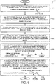
- FIG 9 is a flowchart of a method 200 in accordance with one novel aspect.
- a summing node reference current is supplied onto a summing node of a current driver circuit.
- the summing node reference current 99 on the summing node 87 is maintained at a stable and constant current level by the summing node reference current generator circuit 73.
- the current level is a first factor 108 times the reference current I REF 88 (for example, "2 x I REF ").
- a second step an output voltage of a current driver circuit is detected during an operating mode.
- the output voltage is present on an output nodeof the current driver circuit.
- the output voltage V OUT 67 present between the output node 84 and the ground node 56 is detected by the voltage detector circuit 70.
- the voltage detector circuit 70 is a source follower circuit.
- a replica voltage is generated from the detected output voltage.
- the replica voltage is supplied onto a replica node.
- the voltage detector circuit 70 generates a replica voltage 90 that is supplied onto the replica node 83.
- the replica voltage 90 changes proportionally with respect to the output voltage V OUT 67.
- an output model current is generated using the replica voltage that is present on the replica node.
- the output model current is supplied onto a summing node.
- the OMCM circuit 71 receives the replica voltage 90 from the replica node 83 and generates therefrom an output model current I S 93.
- the OMCM circuit 71 supplies the generates output model current I S 93 onto the summing node 87.
- a corrected current is generated using the output model current and the summing node reference current.
- the corrected current is a difference between the summing node reference current and the output model current.
- the CCM circuit 72 generates a corrected current I C 98 that is supplied onto the summing node 87. Because the summing node 87 is maintained at the constant current level ("2 x I REF "), as the output model current I S 93 decreases, this causes the corrected current I C 98 to increase in a corresponding fashion.
- a gate voltage is generated and supplied onto a current driver transistor.
- the gate voltage is generated from a current proportional to the corrected current.
- the current driver transistor is part of the current driver circuit and has a terminal coupled to the output node.
- the CCM circuit 72 generates a scaled corrected current I D 97 and supplies the scaled corrected current I D 97 onto the CCGVC circuit 74.
- the scaled corrected current I D 97 has a current level that is a second factor 109 times the corrected current I C 98, for example "15 x I C ".
- the scaled corrected current I D 97 is proportional to the corrected current I C 98.
- the CCGVC circuit 74 receives the scaled corrected current I D 97 and generates therefrom a gate voltage 103 that is supplied onto the gate of the current driver transistor 77.
- the drain of the current driver transistor 77 is coupled to the output node 84 via the drive terminal 62.
- the gate voltage 103 controls the output current I OUT 66 to have a current level that is a third factor 110 times the scaled corrected current I D 97, for example "206 x I D ".
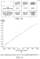
- Figure 10 is a table 300 showing the substantial improvement in stability and size of the output current that is achieved by the current driver 51 as compared to the current drivers 10 and 30.
- the variation of the current through the diode being driven by the current driver 51 is less than five percent when the outputvoltage is anywhere between 0.3 volts and 2.4 volts and significantly smaller in area than current driver 30.
- Figure 11 is a diagram showing how the gate voltage 103 is a function of the corrected current I C 98.
- the gate voltage 103 is supplied onto a gate of the current driver transistor 77 and controls current flow through the diode 54.
- FIG. 12 is a flowchart of a method 400 in accordance with another novel aspect.
- Method 400 is a method of operating the current driver circuit 51.
- a first step 401 identifies the state of various transistors of the current driver I C 51 before the control signal EN 64 is asserted and current is not conducting through the diode 54.
- Steps 402-406 identify a novel current control loop that maintains the output current within five percent of the desired output current level while current is conducting through the diode 54.
- a first step the control signal EN 64 is de-asserted and the transistors 79 and 80 are on.
- Reference current I REF 88 conducts through transistors 81 and 82.
- the summing node reference current 99 is flowing through transistors 106, 107, and 79.
- the transistor 79 maintains transistors 100 and 101 in a non-conductive state.
- Transistor 80 maintains transistors 104 and 105 of the CCGVC circuit 74 in a non-conductive state and transistor 80 also maintains current driver transistor 77 in a non-conductive state.
- Bias current 89 maintains transistor 91 in a conductive state.
- Transistor 92 maintains a voltage on the replica node 83 substantially equal to the output voltage V OUT 67 on the output node 84.
- the output model current I S 93 is flowing in transistors 95, 92, and 94.
- step 402 it is determined whether the control signal EN 64 is asserted. If the control signal EN 64 is de-asserted (for example, a digital logic low level), then the method proceeds to initial step 401. If, on the other hand, the control signal EN 64 is asserted (for example, a digital logic high level), then the method 400 proceeds to the steps of the current control loop 407.
- transistors 79 and 80 are switched from a conductive state to a non-conductive state.
- the control signal EN 64 is supplied onto the gate of the transistor 79 causing transistor 79 to switch off.
- Inverter 78 supplies an inverted version of the control signal EN 64 onto the gate of transistor 80 causing transistor 80 to switch off.
- Transistors 79 and 80 are of opposite conductivity types. For example, transistor 79 is P-type Field Effect Transistor (P-type FET) and transistor 80 is an N-type Field Effect Transistor (N-type FET).
- step 404 output model current I S 93 flows through transistor 96.
- the corrected current I C 98 flows through transistor 100.
- the scaled corrected current I D 97 flows through transistors 101, 104, and 105.
- the output current I OUT 66 flows through diode 54, through current driver transistor 77, and onto ground node 56.
- a fifth step in response to detecting a change in output voltage V OUT 67 on output node 84, transistors 91 and 92 cause the replica voltage 90 on the replica node 83 to match the output voltage V OUT 67 on the output node 84.
- step 406 the adjusted replica voltage 90 adjusts the short channel effect on transistor 93 which in turn adjusts other currents accordingly.
- the method proceeds to step 402 where it is determined whether to remain in the current control loop 407 if the control signal EN 64 is asserted, or to return to the initial step of 401 if the control signal EN 64 is de-asserted.
- the present invention has been described in connection with certain specific embodiments for instructional purposes, the present invention is not limited thereto.
- the current driver IC 51 of Figure 6 sinks current from the LED 54 to ground
- the current driver IC 51 is coupled between the supply node and the LED 54 such that the current driver IC 51 sources current from the supply node 55 through the LED 54, and onto ground node 56.
- the example of Figure 6 uses a Direct Current (DC) voltage source 52 for supplying the LED 54.
- DC Direct Current
- AC Alternating Current
- a rectifier is used to rectify an AC voltage from the AC source.
- a switching regulator receives the rectified AC voltage and supplies a fixed DC voltage onto the supply node 55.
- the current driver IC 51 has only one control terminal 61 onto which the controller IC 53 supplies the control signal EN 64, in other examples, the current driver IC has more than one control terminal.
- the current driver 51 is configured to receive a current control signal.
- the current control indicates a desired output current to send through the LED 54.
- the current control signal is used by the current driver IC 51 to set the various currents ofthe control loop such that the output current I OUT 66 is at the desired current level indicated by the current control signal.
- the supply voltage VDD is between 2.7V and 3.3V and the output voltage V OUT extends approximately 2V. It is appreciated that these voltage ranges are but one example, and in other embodiments, the novel current driver IC 51 can be used with substantially higher voltages (greater than 12V). In other mbodiments, the output voltage V OUT extends over a significantly greater range (more than 10V), yet the novel current driver IC 51 operates to maintain the output current I OUT within five percent of the desired output current level. Accordingly, various modifications, adaptations, and combinations of various features of the described embodiments can be practiced without departing from the scope of the invention as set forth in the claims.
Landscapes
- Engineering & Computer Science (AREA)
- Physics & Mathematics (AREA)
- Microelectronics & Electronic Packaging (AREA)
- General Physics & Mathematics (AREA)
- Nonlinear Science (AREA)
- Electromagnetism (AREA)
- Radar, Positioning & Navigation (AREA)
- Automation & Control Theory (AREA)
- Theoretical Computer Science (AREA)
- Computer Hardware Design (AREA)
- Electronic Switches (AREA)
- Continuous-Control Power Sources That Use Transistors (AREA)
- Control Of Electrical Variables (AREA)
Abstract
Description
- The present disclosure relates generally to current driver circuitry, and more particularly to controlling current flow in current driver applications.
- In typical lighting and light communication applications, a current driver is employed to control current flow through a diode, such as a Light Emitting Diode (LED). In one example, a remote control includes a microcontroller, the current driver, the LED, and a battery that supplies a Direct Current (DC) voltage onto a supply node. One terminal of the LED is coupled to the supply node and another terminal of the LED is coupled in some fashion to the current driver. During operation, the current driver controls an output current that flows through the LED, either by sourcing current from the battery, through the current driver, through the LED and onto a ground node, or by sinking current from the supply node, through the LED, through the current driver, and onto the ground node. Often, the current driver uses a reference current to set a current level of the output current through the LED. The current level of the output current is generally desired to be maintained at a pre- determined multiple of the reference current.
- As current flows through the LED, the battery discharges. Discharging and charging of the battery causes the battery voltage to change over time. In addition, different applications require different battery voltages. Variation in the battery voltage often causes an output voltage between a terminal of the LED and the ground node to vary. The output voltage variation can vary significantly over time due to the charging and discharging of the battery or depending on the voltage and current demands involved in different applications. This variation in the output voltage tends to cause undesirable changes in the current level of the output current flowing through the LED. A solution that overcomes these shortcomings is desirable.
- A system comprises a supply node, a controller integrated circuit (IC), a current driver IC, a diode, and a ground node. The current driver IC is an example of a high current driver that controls currents greater than at least 200 milliamps through the diode. In one example, the diode is a Light Emitting Diode (LED) and the current driver IC is coupled to sink current from the supply node, through the diode, through the current driver IC, and onto the ground node. The LED has an anode coupled to a supply node and a cathode coupled to a drive terminal of the current driver IC. The current driver has a control terminal coupled to receive a control signal EN from the controller IC that enables (turning on the LED) ordisables (turning off the LED) the current driver IC. In one example, the supply node is supplied by Direct Current (DC) source such as a battery. In another example, the supply node is supplied by an Alternating Current (AC) source, such as an AC line.
- During operation, the current driver IC is enabled and sinks an output current from the supply node, through the LED, through the drive terminal, and onto a ground node. An output voltage is present between the cathode of the LED and the ground node. The output voltage typically varies due to charge and discharge cycles of the battery which cause the battery voltage to decrease over time. The output voltage may also vary depending on the voltage and current demands across different applications. In addition, changes in temperature of the LED may also cause the output voltage to change. The current driver IC maintains variation of a current level of the output current to be within five percent of a desired output current level when the output voltage is anywhere within at least a two-volt range. For example, the desired output current level is 250 milliamps, and the current driver IC controls the output current to be between 255 milliamps and 245 milliamps when the output voltage is anywhere between at least 0.3 volts and 2.4 volts.
- In one embodiment, the current driver integrated circuit comprises a voltage detector circuit, an Output Model Current Mirror (OMCM) circuit, a Corrected Current Mirror (CCM) circuit, a summing node reference current generator circuit, a Corrected Current to Gate Voltage Converter (CCGVC) circuit, a summing node, and a current drive transistor. The voltage detector circuit detects an output voltage on an output node and generates a replica voltage.
- The OMCM circuit receives the replica voltage and generates an output model current Is. The output model current IS models a short channel effect on the current driver transistor. The output model current IS is a factor of the reference current IREF modulated by the output voltage VOUT. In this example, the factor is approximately one. The short channel current modulation is caused by short channel effects present on a transistor of the OMCM circuit that is coupled to detect the replica voltage. The transistor of the OMCM circuit that detects the replica voltage has a drain terminal on which the replica voltage is present. The amount of modulation is adjustable by adjusting the length of the transistor that detects the replica voltage. The length of this transistor is adjusted to increase or decrease the amount of short channel current modulation to match that of the current driver transistor.
- In accordance with one novel aspect, the summing node is maintained at a stable current level which is a first factor times a reference current. For example, a current on the summing node is maintained to be twice a reference current ("2xIREF"). The OMCM circuit supplies the output model current Is onto the summing node, and the CCM circuit generates and supplies a corrected current IC onto the summing node. Because the current on the summing node is substantially constant, and because both the output model current IS and the corrected current IC are supplied onto the summing node, as the output model current IS decreases, the corrected current IC increases.
- A scaled corrected current ID is used to generate a gate voltage that controls operation of the current driver transistor. The CCM circuit generates the scaled corrected current ID by scaling the corrected current IC by a second factor. For example, the scaled corrected current ID is fifteen times the corrected current IC. The CCGVC circuit receives the scaled corrected current ID and converts the scaled corrected current ID into a gate voltage. The CCGVC circuit supplies the gate voltage onto a gate terminal of the current driver transistor. The gate voltage controls the conductivity of the current driver transistor such that current flow through the diode remains within five percent of the desired output current level over at least a 2V range of the output voltage. The desired output current level is a third factor times the scaled corrected current ID. For example, the current level of the output current IOUT is two-hundred and six times the scaled corrected current ID. In this way, the increase in corrected current IC compensates for the decrease in output model current due to variation in the output voltage VOUT thereby controlling the current level of the output current IOUT to be maintained within five percent of the desired output current level.
- The foregoing is a summary and thus contains, by necessity, simplifications, generalizations and omissions of detail. Consequently, it is appreciated that the summary is illustrative only. Still other methods, structures and details are set forth in the detailed description below. This summary does not purport to define the invention. The invention is defined by the claims.
- The accompanying drawings, where like numerals indicate like components, illustrate embodiments ofthe invention.
-
Figure 1 is a circuit diagram of acurrent driver circuit 10 having asingle drive transistor 11. -
Figure 2 is a diagram of a top-down view ofdrive transistor 11 shown inFigure 1 . -
Figure 3 is a diagram showing graphs of the output current Iout 18 and reference current IREF 19 versus theoutput voltage V out 20 during operation of thecurrent driver circuit 10 shown inFigure 1 . -
Figure 4 is a circuit diagram of acurrent driver circuit 30 having two highpower output transistors -
Figure 5 is a diagram showing graphs of the output current IOUT 36 andreference current I REF 39 versus theoutput voltage V out 40 during operation of thecurrent driver circuit 30 shown inFigure 4 . -
Figure 6 is a circuit diagram ofsystem 50 involving a novel current driver integratedcircuit 51. -
Figure 7 is a detailed circuit diagram of the current driver integratedcircuit 51 shown inFigure 6 . -
Figure 8 is a graph of current on various nodes versus theoutput voltage V OUT 67 during operation of the current driver integratedcircuit 51 shown inFigure 7 .Figure 9 is a flowchart of amethod 200 in accordance with one novel aspect. -
Figure 10 is a table 300 showing the substantial improvement in stability and size of the output current that is achieved by thecurrent driver 51 as compared to thecurrent drivers -
Figure 11 is a diagram showing how thegate voltage 103 is a function of the correctedcurrent I C 98. -
Figure 12 is a flowchart of amethod 400 in accordance with another novel aspect. - Reference will now be made in detail to exemplary embodiments of the invention, examples of which are illustrated in the accompanying drawings.
-
Figure 1 is a circuit diagram of acurrent driver circuit 10 having asingle drive transistor 11. Thecurrent driver circuit 10 includes a referencecurrent generator 12 and acurrent mirror circuit 13. The current mirror circuit includes the drivefield effect transistor 11 andfield effect transistor 14. A gate terminal oftransistor 14 is coupled to a drain terminal of thetransistor 14. The gate terminal oftransistor 14 is also coupled to a gate terminal of thedrive transistor 11. In the example ofFigure 1 , thedrive transistor 11 is approximately two-hundred ("200") times the size oftransistor 14. Thecurrent driver circuit 10 drives load 15 fromsupply node 16. Aload 15 is coupled between asupply node 16 and a drain terminal of thedrive transistor 11. A source terminal of thedrive transistor 11 is coupled to aground node 17. - During operation of the
current driver circuit 10, thecurrent driver circuit 10 drives theload 15 by sinking current IOUT 18 from asupply node 16 through theload 15 through the drivefield effect transistor 11 and onto aground node 17. The referencecurrent generator circuit 12 outputs a reference current IREF 19 onto a drain terminal of thetransistor 14. The output current IOUT 18 that flows through theload 15 is a factor of the referencecurrent I REF 19. The factor is determined by a ratio of the size of thedrive transistor 11 to the size of thetransistor 14. In this example, the factor is two-hundred ("200") because thedrive transistor 11 is approximately two-hundred ("200") times the size oftransistor 14. The output current IOUT 18 will be 200 times the referencecurrent I REF 19. In this example, the reference current IREF 19 is approximately 1.2 milliamps and the output current IOUT 18 will be approximately 240 milliamps. - In most applications of
current driver circuit 10, it is desirable for the output current IOUT 18 to remain constant and at a fixed factor of the reference current IREF 19 across a range ofoutput voltage V OUT 20. However, during operation of thecurrent driver circuit 10, the output current IOUT 18 tends to change as theoutput voltage V OUT 20 changes. As shown inFigure 3 , the output current IOUT 18 varies approximately 90 milliamps over a 2V range ofoutput voltage 20. -
Figure 2 is a diagram of a top-down view ofdrive transistor 11 shown inFigure 1 . Thedrive transistor 11 includes apolysilicon gate 21, adrain region 22, and asource region 23. The variation of the output current IOUT 18 can be minimized by increasing length L of thepolysilicon gate 21. However, increasing the length L requires increasing the width W to maintain the same width to length ratio of thedrive transistor 11, which in turn, increases the overall size ofdrive transistor 11. Increasing the size ofdrive transistor 11 is generally undesirable due to increased die area that would be consumed by thedrive transistor 11. For example, if the width W increases by a factor of two ("2"), then the length L would also be increased by a factor of two ("2") to maintain the width to length ratio. Thus, in this example, an overall die area of the transistor would increase by a factor of four ("4"). -
Figure 3 is a diagram showing graphs of the output current Iout 18 and reference current IREF 19 versus theoutput voltage V out 20 during operation of thecurrent driver circuit 10 shown inFigure 1 . Theoutput voltage V out 20 extends approximately 2V ranging from 0.4 V to 2.4V. The reference current IREF 19 is set at a constant 1.2 milliamps over the range of output voltages. The output current extends from around 185 milliamps to approximately 275 milliamps over the range of output voltages. Thecurrent driver circuit 10 shown inFigure 1 has an output current 18 that varies approximately 90 milliamps over a 2.0V range of output voltages. As identified by dashedline 24, when theoutput voltage V out 20 is less than 0.6V, the output current Iout 18 increases much more rapidly as compared to when theoutput voltage V OUT 20 is greaterthan 0.6 V. -
Figure 4 is a circuit diagram of acurrent driver circuit 30 having two highpower output transistors Current driver circuit 30 comprises a referencecurrent generator 33, thedrive transistor 31, and thecascode transistor 32. A drain terminal of thecascode transistor 32 is coupled to load 35. A source terminal of thecascode transistor 32 is coupled to a drain terminal of thedrive transistor 31. During operation, thecurrent driver circuit 30 sinks an output current IOUT 36 from thesupply node 37, throughload 35, throughcascode transistor 32, throughdrive transistor 31, and onto aground node 38. The referencecurrent generator 33 outputs a reference current IREF 39 onto a drain terminal of thetransistor 34. The output current IOUT 36 is a factor of the referencecurrent I REF 39. The factor depends upon a width to length ratio of thedrive transistor 31 and a width to length ratio oftransistor 34. Anoutput voltage V OUT 40 is present between a drain terminal of thecascode transistor 32 and a source terminal of thedrive transistor 31. In this example, thecascode transistor 32 and thedrive transistor 31 are each two-hundred ("200") times a sizeof thetransistor 34. -
Figure 5 is a diagram showing graphs of the output current IOUT 36 and reference current IREF 39 versus theoutput voltage V out 40 during operation of thecurrent driver circuit 30 shown inFigure 4 . The output current IOUT 36 tends to vary depending on theoutput voltage V OUT 40. As identified by dashedline 41, when theoutput voltage V out 40 is less than 0.8V, the output current Iout 36 increases much more rapidly as compared to when theoutput voltage V OUT 40 is greater than 0.8 V. Over a range of 2V of theoutput voltage V OUT 40, the current IOUT 36 of thecurrent driver circuit 30 varies by approximately 100 milliamps. -
Figure 6 is a circuit diagram ofsystem 50 involving a novel current driver integratedcircuit 51.System 50 comprises the current driver integratedcircuit 51, abattery 52, a controller integratedcircuit 53, adiode 54, asupply node 55, and aground node 56. Thebattery 52 has a positive terminal that is coupled to thesupply node 55, and a negative terminal that is coupled to theground node 56. Thebattery 52 controls thesupply node 55 to be at a fixed voltage VDD. For example, VDD is between 2.7 V and 3.3 V. In this example,diode 54 is a light emitting diode (LED). In one example,system 50 is part of a remote control in which current is pulsed through the diode thereby radiating energy used in wireless communication. - The controller integrated
circuit 53 has asupply terminal 57, acontrol terminal 58, and aground terminal 59. Thesupply terminal 57 of the controller integratedcircuit 53 is coupled to thesupply node 55. Theground terminal 59 of the controller integratedcircuit 53 is coupled to theground node 56. The current driver integratedcircuit 51 has asupply terminal 60, acontrol terminal 61, adrive terminal 62, and aground terminal 63. Thesupply terminal 60 of the current driver integratedcircuit 51 is coupled to thesupply node 55. Theground terminal 63 of the current driver integratedcircuit 51 is coupled to theground node 56. Thecontrol terminal 61 of the current driver integratedcircuit 51 is coupled to thecontrol terminal 58 of the controller integratedcircuit 53. In one example, thecurrent driver IC 51 is an integrated circuit die and the terminals 60-63 are bond pads. -
Diode 54 has an anode terminal A that is coupled to thesupply node 55.Diode 54 has a cathode terminal C that is coupled to thedrive terminal 62 of the current driver integratedcircuit 51. In the example ofFigure 6 , the controller integratedcircuit 53 and current driver integratedcircuit 51 are supplied by a direct current (DC) source, however, in other embodiments the controller integratedcircuit 53 and the current driver integratedcircuit 51 are supplied from an Alternating Current (AC) source. - During operation, the
diode 54 is initially off and in a non-conductive state such that no current is flowing throughdiode 54. Next, the controller integratedcircuit 53 determines that thediode 54 is to switch from a non-conductive state to a conductive state such that current is to flow through thediode 54. Controller integratedcircuit 53 asserts acontrol signal EN 64 that is supplied from thecontrol terminal 58 onto thecontrol terminal 61 of the current driver integratedcircuit 51 viaconductor 64. In response to detecting thecontrol signal EN 64 switching from a digital logic low level to a digital logic high-level, the current driver integratedcircuit 51 sinks current from thesupply node 55 through thediode 66, and onto theground node 56 through the current driver integratedcircuit 51. Current flows from the supplyingnode 55, onto the anode terminal ofdiode 54, through thediode 54 and out of the cathode terminal of thediode 54, onto thedrive terminal 62 of the current driver integratedcircuit 51, through the current driver integratedcircuit 51, out of theground terminal 63, and onto theground node 56. Anoutput voltage V OUT 67 is present between conductor 68 andground node 56. - In accordance with one novel aspect, the current driver integrated
circuit 51 drives thediode 54 such that the output current IOUT 66 varies by less than 10% over a range ofoutput voltage V OUT 67. For example, the battery voltage might start out at 3.6V and a typical voltage drop across the LED might be 1.2V, so theoutput voltage V OUT 67 would be 2.4V. If the battery discharges to 1.8V, then theoutput voltage V OUT 67 could decrease to 0.6V. Despite the variation in theoutput voltage V OUT 67, the output current IOUT 66 remains within a desired output current range where theoutput voltage V OUT 67 ranges between 0.4V and 2.4V (or a 2V range). In one example, the current driver integratedcircuit 51 drives thediode 54 such that the output current IOUT 66 varies by less than four percent over at least a two-volt range ofoutput voltages V OUT 67. In another example, the current driver integratedcircuit 51 drives thediode 54 such that the output current IOUT 66 varies by less than ten percent over at least a two-volt range ofoutput voltages V OUT 67. -
Figure 7 is a detailed circuit diagram of the current driver integratedcircuit 51 shown inFigure 6 . The current driver integratedcircuit 51 comprisesvoltage detector circuit 70, an Output Model Current Mirror (OMCM)circuit 71, a Corrected Current Mirror (CCM)circuit 72, a summing node referencecurrent generator circuit 73, a Corrected Current To Gate Voltage Converter (CCGVC)circuit 74, a referencecurrent generator 75, a biascurrent generator 76, acurrent drive transistor 77, aninverter 78,transistors replica node 83, anoutput node 84, a referencecurrent node 85, a biascurrent node 86, and a summingnode 87. The referencecurrent generator 75 generates and outputs a reference current IREF 88 onto the referencecurrent node 85. The biascurrent generator 76 generates and outputs a bias current IBIAS 89 on to the biascurrent node 86. - The
voltage detector circuit 70 detects theoutput voltage V OUT 67 on theoutput node 84 and generates areplica voltage 90. Thevoltage detector circuit 70 outputs the generatedreplica voltage 90 onto thereplica node 83. Thevoltage detector circuit 70 comprises a first transistor 91 and asecond transistor 92. A drain terminal and a gate terminal of first transistor 91 are coupled to the biascurrent node 86 and receives the biascurrent I BIAS 89. A source terminal of the first transistor 91 is coupled to theoutput node 84. A gate of the first transistor 91 is coupled to a gate of thesecond transistor 92. The detectedoutput voltage V OUT 67 plus the voltage required to turn on the first transistor 91 is received onto the gate of thesecond transistor 92. A drain terminal of thesecond transistor 92 is coupled to theOMCM circuit 71 and a source terminal of thesecond transistor 92 is coupled to thereplica node 83. - The Output Model Current Mirror (OMCM)
circuit 71 receives thereplica voltage 90 generated by thevoltage detector circuit 70 and generates an output model current Is 93. The output model current IS 93 is supplied onto the summingnode 87. The output model current IS 93 is also referred to as a model short channel effect current because it models a short channel effect on thecurrent driver transistor 77. TheOMCM circuit 71 outputs the generated output model current IS 93 onto thesummingnode 87. The output model current IS 93 is a factor of the IREF current88 modulated by theoutput voltage V OUT 67. In this example, the factor is approximately one. The short channel current modulation is due to short channel effects present ontransistor 94. The amount of modulation is adjusted by adjusting the length oftransistor 94 to increase or decrease the amount of short channel current modulation to match that ofcurrent driver transistor 77. - The
OMCM circuit 71 comprises afirst transistor 94,second transistor 95, and athird transistor 96. Thesecond transistor 95 and thethird transistor 96 form a current mirror. The gate of thesecond transistor 95 is coupled to the gate of thethird transistor 96 and to a drain terminal of thesecond transistor 95. The gates of both thesecond transistor 95 and thethird transistor 96 are coupled to a drain terminal of thesecond transistor 92 of thevoltage detector circuit 70. Source terminals of thesecond transistor 95 and thethird transistor 96 are coupled to thesupply node 55 via thesupply terminal 60. A drain terminal of thethird transistor 96 is coupled to the summingnode 87. - The Corrected Current Mirror (CCM)
circuit 72 generates a scaled corrected current 97. TheCCM circuit 72 generates the scaled corrected current 97 by scaling a corrected current 98. The corrected current 98 is supplied onto the summingnode 87. A summing node reference current 99 is present on the summingnode 87. The summing node reference current 99 is fixed and independent of the supply voltage VDD. The summing node reference current 99 is a sum of the output model current IS 93 and the correctedcurrent I C 98. The corrected current IC 98 is a difference between the summing node reference current 99 and the output model current IS 93. - The
CCM circuit 72 comprises a current mirror that includes afirst transistor 100 and asecond transistor 101. Source terminals of thefirst transistor 100 and thesecond transistor 101 are coupled to the supply node 55via thesupply terminal 60. Gates of thefirst transistor 100 and thesecond transistor 101 are coupled to the drain terminal of thefirst transistor 100 and to the summingnode 87. A drain terminal of thesecond transistor 101 is coupled to agate voltage node 102. - The Corrected Current to Gate Voltage Converter (CCGVC)
circuit 74 receives the scaled correctedcurrent I D 97. TheCCGVC circuit 74 converts the scaled corrected current ID 97 onto agate voltage 103. TheCCGVC circuit 74 supplies the generatedgate voltage 103 onto a gate terminal of thecurrent driver transistor 77. Thegate voltage 103 is a function of the scaled correctedcurrent I D 97. Thegate voltage 103 controls the conductivity of thecurrent driver transistor 77 and in turn, controls current flow through thediode 54. - The
CCGVC circuit 74 comprises afirst transistor 104 and a second transistor 105. A drain terminal of thefirst transistor 104 is coupled togate voltage node 102. A source terminal of thefirst transistor 104 is coupledto a drain terminal of the second transistor 105. A gate of thefirst transistor 104 is coupled to the biascurrent node 86 and to the gate of the first transistor 91 of thevoltage detector circuit 70. A gate terminal of the second transistor 105 is coupled to thegate voltage node 102. A source terminal of the second transistor 105 is coupled to theground node 56 via theground terminal 63. - The summing node reference
current generator circuit 73 generates the summing node reference current 99 on the summingnode 87. The referencecurrent generator circuit 73 comprises a first transistor 106 and a second transistor 107. The summing node referencecurrent generatorcircuit 73 maintains a current level of the summing node reference current 99 on the summingnode 87 to be at a current level equal to the reference current IREF 88 times afirstfactor 108. In this example the first factor is two ("2") and consequently the summing node reference current 99 is maintained to be twice the referencecurrent I REF 88. Because this summing node reference current 99 on the summingnode 87 is maintained at twice the reference current IREF 88, the output model current IS 93 and corrected current IC 98 supplied onto the summingnode 87 change in an opposite manner. For example, a decrease in the output model current 93 during the operating mode results in a corresponding increase in the correctedcurrent I C 98. As theoutput voltage V OUT 67 decreases mainly due todischarge ofbattery 52, the output model current IS 93 tends to decrease. In response, the corrected current IC 98 increases thereby causing the output current 66 to remain within five percent of the desired output current overat least a 2V range of theoutput voltage 67. -
Figure 8 is a graph of current on various nodes versus theoutput voltage V OUT 67 during operation of the current driver integratedcircuit 51 shown inFigure 7 . The desired current level of the output current IOUT 66 is approximately 250.0 milliamps. As shown inFigure 8 , the current level of the output current IOUT 66 remains within +/- 5.0 milliamps of the desired current level. Due to the novel control technique, the output current IOUT 66 varies less than +/- 2% of the desired current level when theoutput voltage V OUT 67 is between 0.3 volts and 2.4 volts. The current driver integratedcircuit 51 yields a substantially more stable output current as compared to thecurrent driver 10 shown inFigure 1 and compared to thecurrent driver 30 shown inFigure 4 . -
Figure 9 is a flowchart of amethod 200 in accordance with one novel aspect. In a first step (step 201), a summing node reference current is supplied onto a summing node of a current driver circuit. For example, in thecurrent driver IC 51 ofFigure 7 , the summing node reference current 99 on the summingnode 87 is maintained at a stable and constant current level by the summing node referencecurrent generator circuit 73. The current level is afirst factor 108 times the reference current IREF 88 (for example, "2 x IREF"). - In a second step (step 202), an output voltage of a current driver circuit is detected during an operating mode. The output voltage is present on an output nodeof the current driver circuit. In the example of the
current driver IC 51 ofFigure 7 , theoutput voltage V OUT 67 present between theoutput node 84 and theground node 56 is detected by thevoltage detector circuit 70. In one example, thevoltage detector circuit 70 is a source follower circuit. - In a third step (step 203), a replica voltage is generated from the detected output voltage. The replica voltage is supplied onto a replica node.
- In the example of
Figure 7 , thevoltage detector circuit 70 generates areplica voltage 90 that is supplied onto thereplica node 83. Thereplica voltage 90 changes proportionally with respect to theoutput voltage V OUT 67. - In a fourth step (step 204), an output model current is generated using the replica voltage that is present on the replica node. The output model current is supplied onto a summing node. In the example of
Figure 7 , theOMCM circuit 71 receives thereplica voltage 90 from thereplica node 83 and generates therefrom an output model current IS 93. TheOMCM circuit 71 supplies the generates output model current IS 93 onto the summingnode 87. - In a fifth step (step 205), a corrected current is generated using the output model current and the summing node reference current. The corrected current is a difference between the summing node reference current and the output model current. In the example of
Figure 7 , theCCM circuit 72 generates a corrected current IC 98 that is supplied onto the summingnode 87. Because the summingnode 87 is maintained at the constant current level ("2 x IREF"), as the output model current IS 93 decreases, this causes the corrected current IC 98 to increase in a corresponding fashion. - In a sixth step (step 206), a gate voltage is generated and supplied onto a current driver transistor. The gate voltage is generated from a current proportional to the corrected current. The current driver transistor is part of the current driver circuit and has a terminal coupled to the output node. For example, in the
current driver IC 51 ofFigure 7 , theCCM circuit 72 generates a scaled corrected current ID 97 and supplies the scaled corrected current ID 97 onto theCCGVC circuit 74. The scaled corrected current ID 97 has a current level that is asecond factor 109 times the corrected current IC 98, for example "15 x IC". The scaled corrected current ID 97 is proportional to the correctedcurrent I C 98. TheCCGVC circuit 74 receives the scaled correctedcurrent I D 97 and generates therefrom agate voltage 103 that is supplied onto the gate of thecurrent driver transistor 77. The drain of thecurrent driver transistor 77 is coupled to theoutput node 84 via thedrive terminal 62. Thegate voltage 103 controls the output current IOUT 66 to have a current level that is athird factor 110 times the scaled corrected current ID 97, for example "206 x ID". -
Figure 10 is a table 300 showing the substantial improvement in stability and size of the output current that is achieved by thecurrent driver 51 as compared to thecurrent drivers current driver 51 is less than five percent when the outputvoltage is anywhere between 0.3 volts and 2.4 volts and significantly smaller in area thancurrent driver 30. -
Figure 11 is a diagram showing how thegate voltage 103 is a function of the correctedcurrent I C 98. Thegate voltage 103 is supplied onto a gate of thecurrent driver transistor 77 and controls current flow through thediode 54. -
Figure 12 is a flowchart of amethod 400 in accordance with another novel aspect.Method 400 is a method of operating thecurrent driver circuit 51. A first step 401 identifies the state of various transistors of the current driver IC 51 before thecontrol signal EN 64 is asserted and current is not conducting through thediode 54. Steps 402-406 identify a novel current control loop that maintains the output current within five percent of the desired output current level while current is conducting through thediode 54. - In a first step (step 401), the
control signal EN 64 is de-asserted and thetransistors transistors 106, 107, and 79. Thetransistor 79 maintainstransistors Transistor 80 maintainstransistors 104 and 105 of theCCGVC circuit 74 in a non-conductive state andtransistor 80 also maintainscurrent driver transistor 77 in a non-conductive state. Bias current 89 maintains transistor 91 in a conductive state.Transistor 92 maintains a voltage on thereplica node 83 substantially equal to theoutput voltage V OUT 67 on theoutput node 84. The output model current IS 93 is flowing intransistors - In a second step (step 402), it is determined whether the
control signal EN 64 is asserted. If thecontrol signal EN 64 is de-asserted (for example, a digital logic low level), then the method proceeds to initial step 401. If, on the other hand, thecontrol signal EN 64 is asserted (for example, a digital logic high level), then themethod 400 proceeds to the steps of thecurrent control loop 407. - In a third step (step 403),
transistors control signal EN 64 is supplied onto the gate of thetransistor 79 causingtransistor 79 to switch off.Inverter 78 supplies an inverted version of thecontrol signal EN 64 onto the gate oftransistor 80 causingtransistor 80 to switch off.Transistors transistor 79 is P-type Field Effect Transistor (P-type FET) andtransistor 80 is an N-type Field Effect Transistor (N-type FET). - In a fourth step (step 404), output model current IS 93 flows through
transistor 96. The corrected current IC 98 flows throughtransistor 100. The scaled corrected current ID 97 flows throughtransistors diode 54, throughcurrent driver transistor 77, and ontoground node 56. - In a fifth step (step 405), in response to detecting a change in
output voltage V OUT 67 onoutput node 84,transistors 91 and 92 cause thereplica voltage 90 on thereplica node 83 to match theoutput voltage V OUT 67 on theoutput node 84. - In a sixth step (step 406), the adjusted
replica voltage 90 adjusts the short channel effect ontransistor 93 which in turn adjusts other currents accordingly. Next, the method proceeds to step 402 where it is determined whether to remain in thecurrent control loop 407 if thecontrol signal EN 64 is asserted, or to return to the initial step of 401 if thecontrol signal EN 64 is de-asserted. - Although the present invention has been described in connection with certain specific embodiments for instructional purposes, the present invention is not limited thereto. For example, although the
current driver IC 51 ofFigure 6 sinks current from theLED 54 to ground, in other embodiments, thecurrent driver IC 51 is coupled between the supply node and theLED 54 such that thecurrent driver IC 51 sources current from thesupply node 55 through theLED 54, and ontoground node 56. - The example of
Figure 6 uses a Direct Current (DC)voltage source 52 for supplying theLED 54. In another example, an Alternating Current (AC) source is used to supply theLED 54. For example, a rectifier is used to rectify an AC voltage from the AC source. A switching regulator receives the rectified AC voltage and supplies a fixed DC voltage onto thesupply node 55. - Although the
current driver IC 51 has only onecontrol terminal 61 onto which thecontroller IC 53 supplies thecontrol signal EN 64, in other examples, the current driver IC has more than one control terminal. For example, in another embodiment, thecurrent driver 51 is configured to receive a current control signal. The current control indicates a desired output current to send through theLED 54. The current control signal is used by thecurrent driver IC 51 to set the various currents ofthe control loop such that the output current IOUT 66 is at the desired current level indicated by the current control signal. - In the example of
Figure 6 , the supply voltage VDD is between 2.7V and 3.3V and the output voltage VOUT extends approximately 2V. It is appreciated that these voltage ranges are but one example, and in other embodiments, the novelcurrent driver IC 51 can be used with substantially higher voltages (greater than 12V). In other mbodiments, the output voltage VOUT extends over a significantly greater range (more than 10V), yet the novelcurrent driver IC 51 operates to maintain the output current IOUT within five percent of the desired output current level. Accordingly, various modifications, adaptations, and combinations of various features of the described embodiments can be practiced without departing from the scope of the invention as set forth in the claims.
Claims (15)
- An apparatuscomprising:an output node;a ground node;a bias current node;a replica node;a summing node;a current driver transistor;a summing node reference current generator circuit, wherein the summing node reference current generator circuit generates a summing node reference current on the summing node;voltage detector circuit, wherein during an operating mode the voltage detector circuit detects an output voltage on the output node and generates a replica voltage on the replica node;an Output Model Current Mirror (OMCM) circuit,wherein the OMCM circuit receives the replica voltage generated by the voltage detector circuit and generates an output model current, and wherein the output model current is supplied onto the summing node;a Corrected Current Mirror (CCM) circuit that generates a scaled corrected current, wherein the CCM circuit generates the scaled corrected current by scaling a corrected current, and wherein the corrected current is a difference between the summing node reference current and the output model current; anda Corrected Current to Gate Voltage Converter (CCGVC) circuit, wherein the CCGVC circuit converts the scaled corrected current into a gate voltage that is supplied onto the gate of the current driver transistor.
- The apparatus of claim 1, wherein the apparatus is a packaged integrated circuit, wherein the packaged integrated circuit comprises an output integrated circuit package terminal and a ground integrated circuit package terminal, wherein the output integrated circuit package terminal is a part of the output node, and wherein the ground integrated circuit package terminal is a part ofthe ground node.
- The apparatus of claim 1 or 2, wherein the summing node reference current on the summing node is a substantially stable and constant current during the operating mode, wherein the summing node reference current is generated from a current generated by a reference current generator, wherein the summing node reference current is a scaled version of the current generated by the reference current generator, and wherein the gate voltage is a function of the scaled corrected current.
- The apparatus of any of the preceding claims, wherein a decrease in the output model current during the operating mode results ina corresponding increase in the corrected current, and wherein a decrease in the output model current during the operating mode results in a corresponding increase in the scaled corrected current.
- The apparatus of any of the preceding claims, wherein a drain terminalof the current driver transistor is coupled to the output node, and wherein the current driver transistor is anN- channel Field Effect Transistor.
- The apparatus of any of the preceding claims, wherein the voltage detector circuit comprises:a first transistor having a first terminal, a second terminal, and a third terminal, wherein the first terminal is coupled to the bias current node, wherein the second terminal is coupled to the output node, and wherein the third terminal is coupled to the bias current node;anda second transistor having a first terminal, a second terminal, and a third terminal, wherein the first terminal is coupled to a transistor of the output model current mirror circuit, wherein the second terminal is coupled to the replica node, and wherein the third terminal of the second transistor is coupled to the third terminal of the first transistor.
- The apparatus of any of the preceding claims, further comprising:a control terminal, wherein the operating mode is enabled in response to a digital signal on the control terminal switching from a first digital logic level to a second digital logic level;a supply terminal, wherein the referencecurrent generator is supplied by the supply voltage terminal;a ground terminal, wherein the ground terminal is coupled to a source terminal of the current driver transistor; anda drive terminal, wherein the drive terminal is coupled to a drain terminal of the current driver transistor.
- The apparatus of any of the preceding claims, wherein the output node is coupled to a cathode of a diode, and wherein during the operating mode the current driver transistor sinkscurrent from the diode to the ground node,
and/or
wherein during the operating mode an output current on the output node varies lessthan five percent when an output voltage is between 0.3 volts and 2.4 volts, and wherein the output voltage is present between the output node and the ground node. - A method comprising:(a) supplying a summing node reference current on to a summing node of a current driver circuit;(b) detecting an output voltage on an output node of the current driver circuit during an operating mode of a current driver circuit;(c) generating a replica voltage from the output voltage detected in (b), wherein the replica voltage is supplied onto a replica node;(d) generating an output model current using the replica voltage present on the replica node, wherein the output model current is supplied onto the summing node;(e) generating a corrected current using the output model current and the summing node reference current, wherein the corrected current is a difference between the summing node reference current and the output model current; and(f) generating and supplying a gate voltage onto a current driver transistor, wherein the gate voltage is generated from a current proportional to the corrected current, wherein the current driver transistor is part of the current driver circuit, and wherein the currentdriver transistor has a terminal coupled to the output node.
- The method of claim 9, wherein the replica voltage generated in (c) varies proportionally to the output voltage detected in (b) present on the output node ofthe current driver circuit, and wherein the gate voltage is generated using the corrected current generated in (e),
and/or
wherein the output node is coupled to a cathode of a diode, and wherein during the operating mode the current driver circuit causes a current to conduct from the cathode of the diode, through the output node, through the current driver transistor, and to a ground node. - The method of claim 9 or 10, wherein the supplying ofthe summing node reference current in (a) further comprises:(a1) generating a reference current using a reference current generator;(a2) scaling the reference current to generate the summing node reference current, wherein a current levelof the summing node reference current is greater than and proportional to the reference current generated in (al); and(a3) supplying the summing node reference currentto the summing node such that a current level of the summing node remains substantially constant during the operating mode.
- The method of any of the claims 9-11, further comprising:
(h) supplying a bias current onto the voltage detector circuit, wherein the supplying of (h) occurs before the supplying of (a), and wherein the voltage detector circuit is part of the current drivercircuit. - The method of any of the preceding claims 9-12, wherein (a) through (f) in part cause an output current on the output node to vary no more than five percent when the output voltage is between a voltage range, wherein the voltage range extends across at least 2.0 volts, preferably wherein the voltage range extends between 0.3 volts and 2.4 volts.
- An integrated circuit device comprising:an output terminal that is coupled to a terminal of a diode, wherein during a mode of operation of the integrated circuit device an output current is present on the output terminal, and wherein an output voltage is present between the output terminal and a ground terminal; andmeans for limiting a variation of the output current during the mode of operation to be less than five percent when the output voltage is within a voltage range that extends across at least 2.0 volts.
- The integrated circuit device of claim 14 with one or more of the following:wherein the means for limiting comprises a reference current generator, a summing node reference current generator circuit, a voltage detector circuit, an output model current mirror circuit, a corrected current mirror circuit, and a corrected current to gate voltage converter circuit;wherein the voltage range extends from 0.3 volts to 2.4 volts;wherein during the mode of operation of the integrated circuit device the output current conducts from the terminal ofthe diode, through the output terminal, through a transistor, and to a ground node.
Applications Claiming Priority (1)
| Application Number | Priority Date | Filing Date | Title |
|---|---|---|---|
| US15/899,352 US10219339B1 (en) | 2018-02-19 | 2018-02-19 | Current correction techniques for accurate high current short channel driver |
Publications (2)
| Publication Number | Publication Date |
|---|---|
| EP3528237A1 true EP3528237A1 (en) | 2019-08-21 |
| EP3528237B1 EP3528237B1 (en) | 2021-06-02 |
Family
ID=65410810
Family Applications (1)
| Application Number | Title | Priority Date | Filing Date |
|---|---|---|---|
| EP19157716.2A Active EP3528237B1 (en) | 2018-02-19 | 2019-02-18 | Current correction techniques for accurate high current short channel driver |
Country Status (6)
| Country | Link |
|---|---|
| US (2) | US10219339B1 (en) |
| EP (1) | EP3528237B1 (en) |
| JP (1) | JP6762487B2 (en) |
| KR (2) | KR102218222B1 (en) |
| CN (2) | CN113727492B (en) |
| TW (2) | TWI758776B (en) |
Cited By (1)
| Publication number | Priority date | Publication date | Assignee | Title |
|---|---|---|---|---|
| WO2023061970A1 (en) * | 2021-10-14 | 2023-04-20 | Ams-Osram Ag | High-side driver circuit |
Families Citing this family (2)
| Publication number | Priority date | Publication date | Assignee | Title |
|---|---|---|---|---|
| KR102838664B1 (en) * | 2021-08-19 | 2025-07-24 | 삼성전자주식회사 | Semiconductor device and memory device comprising the same |
| KR102841905B1 (en) * | 2023-02-23 | 2025-08-01 | 이화여자대학교 산학협력단 | Light emitting device driver circuit |
Citations (4)
| Publication number | Priority date | Publication date | Assignee | Title |
|---|---|---|---|---|
| US6433528B1 (en) * | 2000-12-20 | 2002-08-13 | Texas Instruments Incorporated | High impedance mirror scheme with enhanced compliance voltage |
| WO2003102708A2 (en) * | 2002-05-30 | 2003-12-11 | Analog Devices, Inc. | Voltage regulator with dynamically boosted bias cuttent |
| US20050099748A1 (en) * | 2003-11-12 | 2005-05-12 | Aemireddy Arvind R. | Reverse conduction protection method and apparatus for a dual power supply driver |
| US20120228934A1 (en) * | 2009-09-02 | 2012-09-13 | Austriamicrosystems Ag | Multi-Current Source and Method for Regulating Current |
Family Cites Families (22)
| Publication number | Priority date | Publication date | Assignee | Title |
|---|---|---|---|---|
| JPH10260207A (en) * | 1997-03-19 | 1998-09-29 | Sony Corp | Power supply display |
| US6897715B2 (en) * | 2002-05-30 | 2005-05-24 | Analog Devices, Inc. | Multimode voltage regulator |
| JP4848689B2 (en) * | 2005-07-11 | 2011-12-28 | セイコーエプソン株式会社 | Semiconductor integrated circuit |
| JP4775016B2 (en) * | 2006-02-09 | 2011-09-21 | 富士電機株式会社 | Switching power supply control circuit |
| JP2008283110A (en) * | 2007-05-14 | 2008-11-20 | Seiko Epson Corp | Current load drive circuit |
| JP5301923B2 (en) * | 2008-08-20 | 2013-09-25 | ローム株式会社 | Load driving device, lighting device, display device |
| US8334660B2 (en) * | 2010-05-19 | 2012-12-18 | Sct Technology, Ltd. | Light source driving circuit with low operating output voltage |
| WO2013191806A1 (en) * | 2012-06-21 | 2013-12-27 | Altoran Chip & Systems Inc. | Light emitting diode driver |
| US8766674B1 (en) * | 2013-03-15 | 2014-07-01 | Qualcomm Incorporated | Current-mode buffer with output swing detector for high frequency clock interconnect |
| CN104065251B (en) * | 2013-03-18 | 2017-03-15 | 意法半导体研发(上海)有限公司 | There is the drive circuit of controlled gate discharge current |
| CN203251283U (en) * | 2013-03-18 | 2013-10-23 | 意法半导体研发(上海)有限公司 | Circuit for discharging gate of driving transistor having drain and source, and circuit for driver |
| KR20140146888A (en) * | 2013-06-18 | 2014-12-29 | 삼성전기주식회사 | Light emitting diode lighting apparatus and driving method thereof |
| JP2015128236A (en) * | 2013-12-27 | 2015-07-09 | キヤノン株式会社 | Differential signal drive circuit |
| US20150351170A1 (en) * | 2014-05-28 | 2015-12-03 | Screen Labs America, Inc. | Methods systems and devices for minimizing power losses in light emitting diode drivers |
| JP2015046193A (en) * | 2014-11-27 | 2015-03-12 | ピーエスフォー ルクスコ エスエイアールエルPS4 Luxco S.a.r.l. | Constant current source circuit |
| JP2017059825A (en) * | 2015-09-15 | 2017-03-23 | パナソニックIpマネジメント株式会社 | Semiconductor light source driving device and projection type video display device |
| US10004117B2 (en) * | 2015-09-22 | 2018-06-19 | Nxp B.V. | Amplifier for a constant-current LED driver circuit and constant-current LED driver IC device |
| US9645594B2 (en) * | 2015-10-13 | 2017-05-09 | STMicroelectronics Design & Application S.R.O. | Voltage regulator with dropout detector and bias current limiter and associated methods |
| US9661695B1 (en) * | 2015-11-12 | 2017-05-23 | Hong Kong Applied Science and Technology Research Institute Company Limited | Low-headroom constant current source for high-current applications |
| CA3014830A1 (en) * | 2015-12-08 | 2017-06-15 | Eaton Intelligent Power Limited | Constant power supply for thermo-electric cells |
| US10337676B2 (en) * | 2015-12-09 | 2019-07-02 | Jiaxing Super Lighting Electric Appliance Co., Ltd. | LED tube lamp |
| CN107371299B (en) * | 2017-08-29 | 2023-09-19 | 无锡麟力科技有限公司 | A high power factor linear constant current LED driving circuit and driving method |
-
2018
- 2018-02-19 US US15/899,352 patent/US10219339B1/en active Active
-
2019
- 2019-01-04 US US16/239,725 patent/US10375784B1/en active Active
- 2019-02-08 KR KR1020190015034A patent/KR102218222B1/en active Active
- 2019-02-15 TW TW109123274A patent/TWI758776B/en active
- 2019-02-15 TW TW108105026A patent/TWI701973B/en active
- 2019-02-18 EP EP19157716.2A patent/EP3528237B1/en active Active
- 2019-02-19 CN CN202111036183.9A patent/CN113727492B/en active Active
- 2019-02-19 CN CN201910120792.9A patent/CN110177406B/en active Active
- 2019-02-19 JP JP2019027415A patent/JP6762487B2/en not_active Expired - Fee Related
-
2021
- 2021-02-15 KR KR1020210019805A patent/KR102460738B1/en active Active
Patent Citations (4)
| Publication number | Priority date | Publication date | Assignee | Title |
|---|---|---|---|---|
| US6433528B1 (en) * | 2000-12-20 | 2002-08-13 | Texas Instruments Incorporated | High impedance mirror scheme with enhanced compliance voltage |
| WO2003102708A2 (en) * | 2002-05-30 | 2003-12-11 | Analog Devices, Inc. | Voltage regulator with dynamically boosted bias cuttent |
| US20050099748A1 (en) * | 2003-11-12 | 2005-05-12 | Aemireddy Arvind R. | Reverse conduction protection method and apparatus for a dual power supply driver |
| US20120228934A1 (en) * | 2009-09-02 | 2012-09-13 | Austriamicrosystems Ag | Multi-Current Source and Method for Regulating Current |
Cited By (1)
| Publication number | Priority date | Publication date | Assignee | Title |
|---|---|---|---|---|
| WO2023061970A1 (en) * | 2021-10-14 | 2023-04-20 | Ams-Osram Ag | High-side driver circuit |
Also Published As
| Publication number | Publication date |
|---|---|
| JP6762487B2 (en) | 2020-09-30 |
| KR102460738B1 (en) | 2022-10-31 |
| KR20210020057A (en) | 2021-02-23 |
| EP3528237B1 (en) | 2021-06-02 |
| TWI701973B (en) | 2020-08-11 |
| JP2019164771A (en) | 2019-09-26 |
| US10219339B1 (en) | 2019-02-26 |
| CN110177406B (en) | 2021-09-28 |
| CN110177406A (en) | 2019-08-27 |
| TW202046823A (en) | 2020-12-16 |
| US10375784B1 (en) | 2019-08-06 |
| US20190261476A1 (en) | 2019-08-22 |
| KR20190100033A (en) | 2019-08-28 |
| TW201946495A (en) | 2019-12-01 |
| TWI758776B (en) | 2022-03-21 |
| KR102218222B1 (en) | 2021-02-22 |
| CN113727492A (en) | 2021-11-30 |
| CN113727492B (en) | 2024-03-22 |
Similar Documents
| Publication | Publication Date | Title |
|---|---|---|
| US12464620B2 (en) | Systems and methods for providing power supply to current controllers associated with LED lighting | |
| US8754617B2 (en) | Reverse shunt regulator | |
| TWI509971B (en) | System and method and controller for output detection and synchronous rectification mechanism for adjusting power supply conversion system | |
| EP3788717B1 (en) | Self-biasing ideal diode circuit | |
| CN103748752B (en) | Start-up circuit | |
| US12457670B2 (en) | Systems and methods for controlling power factors of LED lighting systems | |
| KR102460738B1 (en) | Current correction techniques for accurate high current short channel driver | |
| US7430131B2 (en) | Start-up circuit for providing a start-up voltage to an application circuit | |
| US7573251B2 (en) | AC-to-DC voltage regulator | |
| JP4214484B2 (en) | DC power supply | |
| US20230021333A1 (en) | Synchronous rectifier controller and control method used for adjusting a voltage of a control terminal of a rectifier switch | |
| CN119452553A (en) | FET-Based AC-to-DC Converter Utilizing Negative Cycle Gate Pre-Charging | |
| CN100379134C (en) | Boost Switching Regulator Circuit | |
| CN116054364A (en) | Method to maintain synchronous rectification at light load | |
| US11019696B2 (en) | Method and apparatus for operating a semiconductor light source | |
| US7812584B2 (en) | Method for regulating a voltage and circuit therefor | |
| JP2005032260A (en) | Bootstrap capacitor charge circuit with limited charge current | |
| US12267923B2 (en) | Control circuit for bypassing diode current and control method | |
| US20140078786A1 (en) | Power Supply Circuit | |
| JP2007209162A (en) | Dc/dc converter | |
| WO2004100615A1 (en) | Driver circuit for an el lamp |
Legal Events
| Date | Code | Title | Description |
|---|---|---|---|
| PUAI | Public reference made under article 153(3) epc to a published international application that has entered the european phase |
Free format text: ORIGINAL CODE: 0009012 |
|
| STAA | Information on the status of an ep patent application or granted ep patent |
Free format text: STATUS: REQUEST FOR EXAMINATION WAS MADE |
|
| 17P | Request for examination filed |
Effective date: 20190218 |
|
| AK | Designated contracting states |
Kind code of ref document: A1 Designated state(s): AL AT BE BG CH CY CZ DE DK EE ES FI FR GB GR HR HU IE IS IT LI LT LU LV MC MK MT NL NO PL PT RO RS SE SI SK SM TR |
|
| AX | Request for extension of the european patent |
Extension state: BA ME |
|
| STAA | Information on the status of an ep patent application or granted ep patent |
Free format text: STATUS: EXAMINATION IS IN PROGRESS |
|
| 17Q | First examination report despatched |
Effective date: 20200306 |
|
| RAP1 | Party data changed (applicant data changed or rights of an application transferred) |
Owner name: LITTELFUSE, INC. |
|
| RIC1 | Information provided on ipc code assigned before grant |
Ipc: H05B 45/397 20200101ALI20200612BHEP Ipc: G09G 3/14 20060101AFI20200612BHEP Ipc: G05F 3/26 20060101ALI20200612BHEP Ipc: H05B 45/10 20200101ALI20200612BHEP Ipc: H05B 45/345 20200101ALI20200612BHEP |
|
| GRAP | Despatch of communication of intention to grant a patent |
Free format text: ORIGINAL CODE: EPIDOSNIGR1 |
|
| STAA | Information on the status of an ep patent application or granted ep patent |
Free format text: STATUS: GRANT OF PATENT IS INTENDED |
|
| INTG | Intention to grant announced |
Effective date: 20200825 |
|
| GRAJ | Information related to disapproval of communication of intention to grant by the applicant or resumption of examination proceedings by the epo deleted |
Free format text: ORIGINAL CODE: EPIDOSDIGR1 |
|
| STAA | Information on the status of an ep patent application or granted ep patent |
Free format text: STATUS: EXAMINATION IS IN PROGRESS |
|
| INTC | Intention to grant announced (deleted) | ||
| GRAS | Grant fee paid |
Free format text: ORIGINAL CODE: EPIDOSNIGR3 |
|
| STAA | Information on the status of an ep patent application or granted ep patent |
Free format text: STATUS: GRANT OF PATENT IS INTENDED |
|
| GRAP | Despatch of communication of intention to grant a patent |
Free format text: ORIGINAL CODE: EPIDOSNIGR1 |
|
| INTG | Intention to grant announced |
Effective date: 20210311 |
|
| GRAA | (expected) grant |
Free format text: ORIGINAL CODE: 0009210 |
|
| STAA | Information on the status of an ep patent application or granted ep patent |
Free format text: STATUS: THE PATENT HAS BEEN GRANTED |
|
| REG | Reference to a national code |
Ref country code: CH Ref legal event code: EP |
|
| AK | Designated contracting states |
Kind code of ref document: B1 Designated state(s): AL AT BE BG CH CY CZ DE DK EE ES FI FR GB GR HR HU IE IS IT LI LT LU LV MC MK MT NL NO PL PT RO RS SE SI SK SM TR |
|
| REG | Reference to a national code |
Ref country code: GB Ref legal event code: FG4D |
|
| REG | Reference to a national code |
Ref country code: AT Ref legal event code: REF Ref document number: 1399175 Country of ref document: AT Kind code of ref document: T Effective date: 20210615 |
|
| REG | Reference to a national code |
Ref country code: IE Ref legal event code: FG4D |
|
| REG | Reference to a national code |
Ref country code: DE Ref legal event code: R096 Ref document number: 602019004945 Country of ref document: DE |
|
| REG | Reference to a national code |
Ref country code: NL Ref legal event code: FP |
|
| REG | Reference to a national code |
Ref country code: LT Ref legal event code: MG9D |
|
| PG25 | Lapsed in a contracting state [announced via postgrant information from national office to epo] |
Ref country code: BG Free format text: LAPSE BECAUSE OF FAILURE TO SUBMIT A TRANSLATION OF THE DESCRIPTION OR TO PAY THE FEE WITHIN THE PRESCRIBED TIME-LIMIT Effective date: 20210902 Ref country code: FI Free format text: LAPSE BECAUSE OF FAILURE TO SUBMIT A TRANSLATION OF THE DESCRIPTION OR TO PAY THE FEE WITHIN THE PRESCRIBED TIME-LIMIT Effective date: 20210602 Ref country code: HR Free format text: LAPSE BECAUSE OF FAILURE TO SUBMIT A TRANSLATION OF THE DESCRIPTION OR TO PAY THE FEE WITHIN THE PRESCRIBED TIME-LIMIT Effective date: 20210602 Ref country code: LT Free format text: LAPSE BECAUSE OF FAILURE TO SUBMIT A TRANSLATION OF THE DESCRIPTION OR TO PAY THE FEE WITHIN THE PRESCRIBED TIME-LIMIT Effective date: 20210602 |
|
| REG | Reference to a national code |
Ref country code: AT Ref legal event code: MK05 Ref document number: 1399175 Country of ref document: AT Kind code of ref document: T Effective date: 20210602 |
|
| PG25 | Lapsed in a contracting state [announced via postgrant information from national office to epo] |
Ref country code: GR Free format text: LAPSE BECAUSE OF FAILURE TO SUBMIT A TRANSLATION OF THE DESCRIPTION OR TO PAY THE FEE WITHIN THE PRESCRIBED TIME-LIMIT Effective date: 20210903 Ref country code: LV Free format text: LAPSE BECAUSE OF FAILURE TO SUBMIT A TRANSLATION OF THE DESCRIPTION OR TO PAY THE FEE WITHIN THE PRESCRIBED TIME-LIMIT Effective date: 20210602 Ref country code: PL Free format text: LAPSE BECAUSE OF FAILURE TO SUBMIT A TRANSLATION OF THE DESCRIPTION OR TO PAY THE FEE WITHIN THE PRESCRIBED TIME-LIMIT Effective date: 20210602 Ref country code: NO Free format text: LAPSE BECAUSE OF FAILURE TO SUBMIT A TRANSLATION OF THE DESCRIPTION OR TO PAY THE FEE WITHIN THE PRESCRIBED TIME-LIMIT Effective date: 20210902 Ref country code: SE Free format text: LAPSE BECAUSE OF FAILURE TO SUBMIT A TRANSLATION OF THE DESCRIPTION OR TO PAY THE FEE WITHIN THE PRESCRIBED TIME-LIMIT Effective date: 20210602 Ref country code: RS Free format text: LAPSE BECAUSE OF FAILURE TO SUBMIT A TRANSLATION OF THE DESCRIPTION OR TO PAY THE FEE WITHIN THE PRESCRIBED TIME-LIMIT Effective date: 20210602 |
|
| PG25 | Lapsed in a contracting state [announced via postgrant information from national office to epo] |
Ref country code: EE Free format text: LAPSE BECAUSE OF FAILURE TO SUBMIT A TRANSLATION OF THE DESCRIPTION OR TO PAY THE FEE WITHIN THE PRESCRIBED TIME-LIMIT Effective date: 20210602 Ref country code: ES Free format text: LAPSE BECAUSE OF FAILURE TO SUBMIT A TRANSLATION OF THE DESCRIPTION OR TO PAY THE FEE WITHIN THE PRESCRIBED TIME-LIMIT Effective date: 20210602 Ref country code: SK Free format text: LAPSE BECAUSE OF FAILURE TO SUBMIT A TRANSLATION OF THE DESCRIPTION OR TO PAY THE FEE WITHIN THE PRESCRIBED TIME-LIMIT Effective date: 20210602 Ref country code: RO Free format text: LAPSE BECAUSE OF FAILURE TO SUBMIT A TRANSLATION OF THE DESCRIPTION OR TO PAY THE FEE WITHIN THE PRESCRIBED TIME-LIMIT Effective date: 20210602 Ref country code: PT Free format text: LAPSE BECAUSE OF FAILURE TO SUBMIT A TRANSLATION OF THE DESCRIPTION OR TO PAY THE FEE WITHIN THE PRESCRIBED TIME-LIMIT Effective date: 20211004 Ref country code: SM Free format text: LAPSE BECAUSE OF FAILURE TO SUBMIT A TRANSLATION OF THE DESCRIPTION OR TO PAY THE FEE WITHIN THE PRESCRIBED TIME-LIMIT Effective date: 20210602 Ref country code: CZ Free format text: LAPSE BECAUSE OF FAILURE TO SUBMIT A TRANSLATION OF THE DESCRIPTION OR TO PAY THE FEE WITHIN THE PRESCRIBED TIME-LIMIT Effective date: 20210602 Ref country code: AT Free format text: LAPSE BECAUSE OF FAILURE TO SUBMIT A TRANSLATION OF THE DESCRIPTION OR TO PAY THE FEE WITHIN THE PRESCRIBED TIME-LIMIT Effective date: 20210602 |
|
| REG | Reference to a national code |
Ref country code: DE Ref legal event code: R097 Ref document number: 602019004945 Country of ref document: DE |
|
| PLBE | No opposition filed within time limit |
Free format text: ORIGINAL CODE: 0009261 |
|
| STAA | Information on the status of an ep patent application or granted ep patent |
Free format text: STATUS: NO OPPOSITION FILED WITHIN TIME LIMIT |
|
| PG25 | Lapsed in a contracting state [announced via postgrant information from national office to epo] |
Ref country code: DK Free format text: LAPSE BECAUSE OF FAILURE TO SUBMIT A TRANSLATION OF THE DESCRIPTION OR TO PAY THE FEE WITHIN THE PRESCRIBED TIME-LIMIT Effective date: 20210602 |
|
| 26N | No opposition filed |
Effective date: 20220303 |
|
| PG25 | Lapsed in a contracting state [announced via postgrant information from national office to epo] |
Ref country code: AL Free format text: LAPSE BECAUSE OF FAILURE TO SUBMIT A TRANSLATION OF THE DESCRIPTION OR TO PAY THE FEE WITHIN THE PRESCRIBED TIME-LIMIT Effective date: 20210602 |
|
| PG25 | Lapsed in a contracting state [announced via postgrant information from national office to epo] |
Ref country code: IT Free format text: LAPSE BECAUSE OF FAILURE TO SUBMIT A TRANSLATION OF THE DESCRIPTION OR TO PAY THE FEE WITHIN THE PRESCRIBED TIME-LIMIT Effective date: 20210602 |
|
| PG25 | Lapsed in a contracting state [announced via postgrant information from national office to epo] |
Ref country code: MC Free format text: LAPSE BECAUSE OF FAILURE TO SUBMIT A TRANSLATION OF THE DESCRIPTION OR TO PAY THE FEE WITHIN THE PRESCRIBED TIME-LIMIT Effective date: 20210602 |
|
| REG | Reference to a national code |
Ref country code: CH Ref legal event code: PL |
|
| REG | Reference to a national code |
Ref country code: BE Ref legal event code: MM Effective date: 20220228 |
|
| PG25 | Lapsed in a contracting state [announced via postgrant information from national office to epo] |
Ref country code: LU Free format text: LAPSE BECAUSE OF NON-PAYMENT OF DUE FEES Effective date: 20220218 |
|
| PG25 | Lapsed in a contracting state [announced via postgrant information from national office to epo] |
Ref country code: FR Free format text: LAPSE BECAUSE OF NON-PAYMENT OF DUE FEES Effective date: 20220228 |
|
| PG25 | Lapsed in a contracting state [announced via postgrant information from national office to epo] |
Ref country code: LI Free format text: LAPSE BECAUSE OF NON-PAYMENT OF DUE FEES Effective date: 20220228 Ref country code: IE Free format text: LAPSE BECAUSE OF NON-PAYMENT OF DUE FEES Effective date: 20220218 Ref country code: CH Free format text: LAPSE BECAUSE OF NON-PAYMENT OF DUE FEES Effective date: 20220228 |
|
| PG25 | Lapsed in a contracting state [announced via postgrant information from national office to epo] |
Ref country code: BE Free format text: LAPSE BECAUSE OF NON-PAYMENT OF DUE FEES Effective date: 20220228 |
|
| P01 | Opt-out of the competence of the unified patent court (upc) registered |
Effective date: 20230607 |
|
| GBPC | Gb: european patent ceased through non-payment of renewal fee |
Effective date: 20230218 |
|
| PG25 | Lapsed in a contracting state [announced via postgrant information from national office to epo] |
Ref country code: GB Free format text: LAPSE BECAUSE OF NON-PAYMENT OF DUE FEES Effective date: 20230218 |
|
| PG25 | Lapsed in a contracting state [announced via postgrant information from national office to epo] |
Ref country code: GB Free format text: LAPSE BECAUSE OF NON-PAYMENT OF DUE FEES Effective date: 20230218 |
|
| PG25 | Lapsed in a contracting state [announced via postgrant information from national office to epo] |
Ref country code: MK Free format text: LAPSE BECAUSE OF FAILURE TO SUBMIT A TRANSLATION OF THE DESCRIPTION OR TO PAY THE FEE WITHIN THE PRESCRIBED TIME-LIMIT Effective date: 20210602 Ref country code: CY Free format text: LAPSE BECAUSE OF FAILURE TO SUBMIT A TRANSLATION OF THE DESCRIPTION OR TO PAY THE FEE WITHIN THE PRESCRIBED TIME-LIMIT Effective date: 20210602 |
|
| PG25 | Lapsed in a contracting state [announced via postgrant information from national office to epo] |
Ref country code: HU Free format text: LAPSE BECAUSE OF FAILURE TO SUBMIT A TRANSLATION OF THE DESCRIPTION OR TO PAY THE FEE WITHIN THE PRESCRIBED TIME-LIMIT; INVALID AB INITIO Effective date: 20190218 |
|
| PG25 | Lapsed in a contracting state [announced via postgrant information from national office to epo] |
Ref country code: TR Free format text: LAPSE BECAUSE OF FAILURE TO SUBMIT A TRANSLATION OF THE DESCRIPTION OR TO PAY THE FEE WITHIN THE PRESCRIBED TIME-LIMIT Effective date: 20210602 |
|
| PG25 | Lapsed in a contracting state [announced via postgrant information from national office to epo] |
Ref country code: MT Free format text: LAPSE BECAUSE OF FAILURE TO SUBMIT A TRANSLATION OF THE DESCRIPTION OR TO PAY THE FEE WITHIN THE PRESCRIBED TIME-LIMIT Effective date: 20210602 |
|
| PGFP | Annual fee paid to national office [announced via postgrant information from national office to epo] |
Ref country code: NL Payment date: 20241214 Year of fee payment: 7 |
|
| PGFP | Annual fee paid to national office [announced via postgrant information from national office to epo] |
Ref country code: DE Payment date: 20241224 Year of fee payment: 7 |