JP2007209162A - Dc/dc converter - Google Patents

Dc/dc converter Download PDF

Info

Publication number
JP2007209162A
JP2007209162A JP2006026983A JP2006026983A JP2007209162A JP 2007209162 A JP2007209162 A JP 2007209162A JP 2006026983 A JP2006026983 A JP 2006026983A JP 2006026983 A JP2006026983 A JP 2006026983A JP 2007209162 A JP2007209162 A JP 2007209162A
Authority
JP
Japan
Prior art keywords
voltage
switching element
control circuit
output
signal
Prior art date
Legal status (The legal status is an assumption and is not a legal conclusion. Google has not performed a legal analysis and makes no representation as to the accuracy of the status listed.)
Granted
Application number
JP2006026983A
Other languages
Japanese (ja)
Other versions
JP4690213B2 (en
Inventor
Yasutsuna Mitamura
容維 三田村
Current Assignee (The listed assignees may be inaccurate. Google has not performed a legal analysis and makes no representation or warranty as to the accuracy of the list.)
Seiko Instruments Inc
Original Assignee
Seiko Instruments Inc
Priority date (The priority date is an assumption and is not a legal conclusion. Google has not performed a legal analysis and makes no representation as to the accuracy of the date listed.)
Filing date
Publication date
Application filed by Seiko Instruments Inc filed Critical Seiko Instruments Inc
Priority to JP2006026983A priority Critical patent/JP4690213B2/en
Publication of JP2007209162A publication Critical patent/JP2007209162A/en
Application granted granted Critical
Publication of JP4690213B2 publication Critical patent/JP4690213B2/en
Expired - Fee Related legal-status Critical Current
Anticipated expiration legal-status Critical

Links

Images

Abstract

<P>PROBLEM TO BE SOLVED: To provide a DC/DC converter with little consumption current which starts operation from a low voltage, and and also to provide electronic equipment using the DC/DC converter. <P>SOLUTION: When the voltage of a battery 10 is low and has no boosted output, a current control type switching element is used, and when the battery has the boosted output, a voltage control type switching element is used to boost the DC/DC converter from a low voltage. After the DC/DC converter is boosted, the current control type switching element with high power consumption is stopped to reduce the power consumption of the DC/DC converter. The electronic equipment having this DC/DC converter is provided. <P>COPYRIGHT: (C)2007,JPO&INPIT

Description

本発明は電源から入力された電圧を所望の電圧に変換して出力するDC/DCコンバータおよびそのDC/DCコンバータを有する電子機器に関する。   The present invention relates to a DC / DC converter that converts a voltage input from a power source into a desired voltage and outputs the voltage, and an electronic apparatus having the DC / DC converter.

電池などを電源とする電子機器は、電源の電圧をDC/DCコンバータを介して、各機能モジュールが必要とする電圧に変換して使用している。このようなDC/DCコンバータとしてはチョッパ方式のスイッチングレギュレータがある。チョッパ方式のスイッチングレギュレータはコイルに接続したスイッチをオンオフすることで電気エネルギーを充放電させ、その放電出力を平滑して所望の電圧に変換する。   An electronic device using a battery as a power source converts the power source voltage into a voltage required by each functional module through a DC / DC converter. As such a DC / DC converter, there is a chopper type switching regulator. A chopper switching regulator charges and discharges electrical energy by turning on and off a switch connected to a coil, and smoothes the discharge output to convert it into a desired voltage.

図3にチョッパ方式の昇圧型スイッチングレギュレータ回路を用いた従来の回路を示す。昇圧型スイッチングレギュレータ2は図中点線で囲われた部分の回路である。この昇圧型スイッチングレギュレータ2はコイル4と整流素子5と平滑コンデンサ6と制御回路7とNPN型トランジスタ8とベース抵抗9とで構成されている。昇圧型スイッチングレギュレータ2の入力端子は電池1の高電位側端子(プラス端子)と接続され、出力端子は出力負荷3のプラス端子と接続されている。昇圧型スイッチングレギュレータ2は電池1の電圧を昇圧して、出力負荷3へ供給する。   FIG. 3 shows a conventional circuit using a chopper type boosting switching regulator circuit. The step-up switching regulator 2 is a circuit in a portion surrounded by a dotted line in the figure. The step-up switching regulator 2 includes a coil 4, a rectifying element 5, a smoothing capacitor 6, a control circuit 7, an NPN transistor 8, and a base resistor 9. The input terminal of the step-up switching regulator 2 is connected to the high potential side terminal (plus terminal) of the battery 1, and the output terminal is connected to the plus terminal of the output load 3. The step-up switching regulator 2 boosts the voltage of the battery 1 and supplies it to the output load 3.

昇圧型スイッチングレギュレータ2は、入力端子がコイル4の入力端子と接続されている。コイル4の出力端子は、整流素子5の入力端子とNPNトランジスタ8のコレクタとに接続されている。整流素子5の出力端子は、制御回路7の電源端子と平滑コンデンサ6のプラス端子と昇圧型スイッチングレギュレータ2の出力端子とに接続されている。制御回路7の信号出力端子はベース抵抗9を介してNPNトランジスタ8のベースに接続されている。電池1の低電位側端子(マイナス端子)は、NPNトランジスタ8のエミッタと出力負荷3のマイナス端子とに接続されている。平滑コンデンサ6は整流素子5の出力端子と電池1のマイナス端子間に介挿されている。   The step-up switching regulator 2 has an input terminal connected to the input terminal of the coil 4. The output terminal of the coil 4 is connected to the input terminal of the rectifying element 5 and the collector of the NPN transistor 8. The output terminal of the rectifying element 5 is connected to the power supply terminal of the control circuit 7, the plus terminal of the smoothing capacitor 6, and the output terminal of the step-up switching regulator 2. The signal output terminal of the control circuit 7 is connected to the base of the NPN transistor 8 through the base resistor 9. The low potential side terminal (minus terminal) of the battery 1 is connected to the emitter of the NPN transistor 8 and the minus terminal of the output load 3. The smoothing capacitor 6 is interposed between the output terminal of the rectifying element 5 and the negative terminal of the battery 1.

次に図3のチョッパ方式の昇圧型スイッチングレギュレータ回路を用いた従来の回路の動作について説明する。NPNトランジスタ8がオン状態のときは電池1からコイル4へほぼ無負荷で電流が流れる。次にNPNトランジスタ8がオフすると急激に電流が減るので誘導起電力が発生し、電圧が上昇する。その電圧を整流素子5で整流し、平滑コンデンサ6で平滑して昇圧出力とする。NPNトランジスタ8は、制御回路7から出力される駆動パルスをベースに入力することによってオンオフする。NPNトランジスタ8のベース電流はベース抵抗9によって制限される。また、制御回路7では出力電圧を検出して、出力電圧が所定の電圧になるように駆動パルスのデューティーを可変し、トランジスタのオンオフを制御する。このように制御を行い所望の電圧の昇圧出力を得ている。   Next, the operation of a conventional circuit using the chopper type boosting switching regulator circuit of FIG. 3 will be described. When the NPN transistor 8 is on, a current flows from the battery 1 to the coil 4 with almost no load. Next, when the NPN transistor 8 is turned off, the current is rapidly reduced, so that an induced electromotive force is generated and the voltage is increased. The voltage is rectified by the rectifying element 5 and smoothed by the smoothing capacitor 6 to obtain a boosted output. The NPN transistor 8 is turned on / off by inputting the drive pulse output from the control circuit 7 to the base. The base current of the NPN transistor 8 is limited by the base resistor 9. The control circuit 7 detects the output voltage, changes the duty of the drive pulse so that the output voltage becomes a predetermined voltage, and controls the on / off of the transistor. Control is performed in this way to obtain a boosted output of a desired voltage.

また、制御回路の電源として、電源回路への電源投入時には入力される電源を用い、電源回路が動作して所定の電圧が出力されるとその出力を用いる電源切替の回路が開示されている(特許文献1参照)。
特開平8−331839
Further, a power supply switching circuit is disclosed in which a power supply input when power is supplied to the power supply circuit is used as a power supply for the control circuit, and the power supply circuit operates to output a predetermined voltage when the power supply circuit operates. Patent Document 1).
JP-A-8-331839

従来のチョッパ方式の昇圧型スイッチングレギュレータ回路では、バイポーラ型トランジスタやFET(電圧効果型トランジスタ)をスイッチング素子に用いている。これらのスイッチング素子は、入力する制御信号の電圧がスイッチング素子の閾値電圧(VthあるいはVBE)を境に、オンオフする。一般的に、バイポーラ型トランジスタはFETより低電圧(例えば約0.5V)からオンするので、低電圧からの昇圧が可能である。また、FETを用いた場合は、オンオフのために消費する電流はバイポーラ型トランジスタに比べ少ないので、昇圧効率が高い。   In a conventional chopper type step-up switching regulator circuit, a bipolar transistor or FET (voltage effect transistor) is used as a switching element. These switching elements are turned on and off with the threshold voltage (Vth or VBE) of the switching element as a boundary. In general, since a bipolar transistor is turned on from a lower voltage (for example, about 0.5 V) than an FET, boosting from a low voltage is possible. In addition, when the FET is used, the current consumed for on / off is less than that of the bipolar transistor, so that the boosting efficiency is high.

しかしながら、バイポーラ型トランジスタをスイッチング素子に用いると、低電圧から昇圧するために多くのコレクタ電流を必要とするので、そのために多くのベース電流を必要とする。その結果、スイッチング素子での消費電流が多くなり、昇圧効率が悪くなるという問題がある。また、FETをスイッチング素子に用いると、電圧制御であるのでスイッチング素子での消費電流は小さいが、ゲート電圧がVth(例えば約1.0V)を超えないとオンしないので、バイポーラ型トランジスタでは昇圧できる電圧でもFETでは昇圧できないという問題がある。   However, when a bipolar transistor is used as a switching element, a large amount of collector current is required to boost the voltage from a low voltage. Therefore, a large amount of base current is required. As a result, there is a problem that the current consumption in the switching element increases and the boosting efficiency deteriorates. Further, when the FET is used as a switching element, the current consumption in the switching element is small because of voltage control, but it is not turned on unless the gate voltage exceeds Vth (for example, about 1.0 V). There is a problem that even a voltage cannot be boosted by an FET.

上述した開示されている技術(特許文献1)は昇圧のためのスイッチング素子を切替えて使用してはいないので、動作電圧や消費電力の問題を有している。   Since the disclosed technique (Patent Document 1) described above does not use switching elements for boosting, it has problems of operating voltage and power consumption.

本発明は、この2つのスイッチング素子の長所を活かして、電圧制御型スイッチング素子の閾値電圧より低い電圧が入力されても昇圧され、消費電力の少ないDC/DCコンバータ及びそのDC/DCコンバータを用いた電子機器を提供する。   The present invention takes advantage of these two switching elements and uses a DC / DC converter that consumes less power and is boosted even when a voltage lower than the threshold voltage of the voltage controlled switching element is input, and the DC / DC converter. Provide electronic equipment.

本発明は、電源から入力される入力電圧を、所望の出力電圧に変換して出力するDC/DCコンバータにおいて、入力電圧を昇圧するコイルと、そのコイルの一端と電源との間に介挿し、コイルに対して電気エネルギーを充放電させるため、コイルに流れる電流のオンオフ制御を行う、電流制御型スイッチング素子及び電圧制御型スイッチング素子が並列に接続されたスイッチング手段と、昇圧された電気エネルギーを一時的に蓄電するコンデンサと、そのコンデンサに蓄電される出力電圧が予め設定された電圧となるよう、スイッチング手段のオンオフ制御を行うオンオフ信号を出力する制御回路と、出力電圧が入力電圧より低い場合、入力電圧を制御回路の制御電圧とし、一方、出力電圧が入力電圧より高い場合、出力電圧を制御回路の制御電圧とする電源制御回路と、オンオフ信号を電流制御型スイッチング素子に入力させるか否かを、出力電圧に応じて行う駆動制御回路と、を有し、制御回路は駆動制御回路及び電圧制御型スイッチング素子に対して制御電圧の電圧レベルをオンオフ信号の振幅値とし出力する構成を有するDC/DCコンバータである。   The present invention provides a DC / DC converter that converts an input voltage input from a power source into a desired output voltage and outputs the same, and is interposed between a coil that boosts the input voltage, one end of the coil, and the power source, In order to charge and discharge electrical energy to and from the coil, switching means in which a current-controlled switching element and a voltage-controlled switching element are connected in parallel to perform on / off control of the current flowing through the coil, and the boosted electrical energy is temporarily stored. When the output voltage is lower than the input voltage, the capacitor for automatically storing, the control circuit for outputting an on / off signal for performing on / off control of the switching means so that the output voltage stored in the capacitor becomes a preset voltage, If the input voltage is the control voltage of the control circuit and the output voltage is higher than the input voltage, the output voltage is A power supply control circuit for controlling the voltage, and a drive control circuit for determining whether or not to input an on / off signal to the current control type switching element according to the output voltage. The control circuit includes the drive control circuit and the voltage control type. The DC / DC converter has a configuration in which the voltage level of the control voltage is output to the switching element as the amplitude value of the on / off signal.

また本発明では、予め設定された停止電圧を出力電圧が超えた場合、制御回路の制御により電流制御型スイッチング手段のオンオフを停止させる構成にすることができる。   In the present invention, when the output voltage exceeds a preset stop voltage, the current control type switching means can be stopped from being turned on / off by the control of the control circuit.

また本発明では、駆動制御回路が、予め設定された停止電圧を前記出力電圧が超えた場合、オンオフ信号を電流制御型スイッチング素子に入力させず、オフ状態にてオンオフを停止させる構成にすることができる。   In the present invention, the drive control circuit is configured to stop on / off in the off state without inputting the on / off signal to the current control type switching element when the output voltage exceeds a preset stop voltage. Can do.

また本発明では、駆動制御回路が、出力電圧を予め設定された抵抗によって抵抗分割した分圧値が入力電圧以上の場合、オンオフ信号を電流制御型スイッチング素子に入力させず、オフ状態にてオンオフを停止させる構成にすることができる。   Further, in the present invention, when the drive control circuit divides the output voltage by a resistance set in advance and the divided voltage value is equal to or higher than the input voltage, the on / off signal is not input to the current control type switching element and is turned on / off in the off state. Can be configured to stop.

また、駆動制御回路が、オンオフ信号を電流制御型スイッチング素子へ出力する場合、電流制御型スイッチング素子を駆動させるために電源から電力の供給を受けてオンオフ信号を出力する構成にすることができる。   Further, when the drive control circuit outputs an on / off signal to the current control type switching element, it can be configured to receive power supply from a power supply and output the on / off signal in order to drive the current control type switching element.

また、上記電流制御型スイッチング素子はバイポーラ型トランジスタであり、電圧制御型スイッチング素子は電界効果型トランジスタとすることができる。   Further, the current control switching element can be a bipolar transistor, and the voltage control switching element can be a field effect transistor.

また本発明は、上記構成を有するDC/DCコンバータを用いた電子機器である。   The present invention is also an electronic device using the DC / DC converter having the above-described configuration.

上述したように本発明により、電圧制御型スイッチング素子の閾値電圧より低くい電圧から昇圧をし、スイッチング手段における電力消費が少ないDC/DCコンバータを得ることができる。   As described above, according to the present invention, it is possible to obtain a DC / DC converter that boosts voltage from a voltage lower than the threshold voltage of the voltage-controlled switching element and consumes less power in the switching means.

以下本発明の実施形態を図面を用いて説明する。   Embodiments of the present invention will be described below with reference to the drawings.

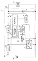
図1は本発明の実施の形態を示したブロック図である。   FIG. 1 is a block diagram showing an embodiment of the present invention.

電池10は直流電源で、二次電池や一次電池や太陽電池などの電池やAC/DCコンバータなどの直流の電源を用いることができる。   The battery 10 is a direct current power supply, and a secondary power supply, a primary battery, a battery such as a solar battery, or a direct current power supply such as an AC / DC converter can be used.

図1中で点線で囲った部分はDC/DCコンバータ11である。DC/DCコンバータ11は入力端子22を介して電池10から電力を入力し、昇圧し、出力端子23を介して出力負荷12へ出力する。DC/DCコンバータ11は出力負荷12で用いる電圧に応じて電圧を変換して出力する。出力負荷12は、映像や音楽を再生する電子機器や、携帯電話などの通信機器や、コンピュータなどの電子機器などの直流電源を必要とする電子機器である。   A portion surrounded by a dotted line in FIG. 1 is a DC / DC converter 11. The DC / DC converter 11 receives electric power from the battery 10 through the input terminal 22, boosts the power, and outputs it to the output load 12 through the output terminal 23. The DC / DC converter 11 converts the voltage according to the voltage used by the output load 12 and outputs it. The output load 12 is an electronic device that requires a DC power source, such as an electronic device that reproduces video or music, a communication device such as a mobile phone, or an electronic device such as a computer.

DC/DCコンバータ11はコイル13、整流素子14、平滑コンデンサ15、駆動制御信号生成回路16、電源制御回路17、制御回路18、駆動制御回路19、電流制御型スイッチング素子20、電圧制御型スイッチング素子21を有し構成している。   The DC / DC converter 11 includes a coil 13, a rectifying element 14, a smoothing capacitor 15, a drive control signal generation circuit 16, a power supply control circuit 17, a control circuit 18, a drive control circuit 19, a current control type switching element 20, and a voltage control type switching element. 21.

コイル13の入力端子は、入力端子22を介して電池10の高電位側端子(プラス端子)、駆動制御信号生成回路16の第一の入力端子、電源制御回路17の第一の入力端子、及び駆動制御回路19の電源入力端子とに接続される。コイル13の出力端子は、電圧制御型スイッチング素子21の第一のスイッチ端子、電流制御型スイッチング素子20の第一のスイッチ端子、及び整流素子14の入力端子とに接続される。   The input terminal of the coil 13 is connected to the high potential side terminal (plus terminal) of the battery 10 via the input terminal 22, the first input terminal of the drive control signal generation circuit 16, the first input terminal of the power supply control circuit 17, and It is connected to the power input terminal of the drive control circuit 19. The output terminal of the coil 13 is connected to the first switch terminal of the voltage controlled switching element 21, the first switch terminal of the current controlled switching element 20, and the input terminal of the rectifying element 14.

電圧制御型スイッチング素子21の第二のスイッチ端子は電池10の低電位側端子(マイナス端子)に接続される。電流制御型スイッチング素子20の第二のスイッチ端子は電池10のマイナス端子に接続される。   The second switch terminal of the voltage control type switching element 21 is connected to the low potential side terminal (minus terminal) of the battery 10. The second switch terminal of the current control type switching element 20 is connected to the negative terminal of the battery 10.

整流素子14の出力端子は、出力端子23を介して出力負荷12のプラス端子、平滑コンデンサ15のプラス端子、駆動制御信号生成回路16の第二入力端子、電源制御回路17の第二入力端子、及び制御回路18の電圧検出端子とに接続される。   The output terminal of the rectifying element 14 is connected to the positive terminal of the output load 12 via the output terminal 23, the positive terminal of the smoothing capacitor 15, the second input terminal of the drive control signal generation circuit 16, the second input terminal of the power supply control circuit 17, And a voltage detection terminal of the control circuit 18.

接続負荷12のマイナス端子は電池10のマイナス端子に接続される。平滑コンデンサ15のマイナス端子は電池10のマイナス端子に接続される。駆動制御信号生成回路16の出力端子は駆動制御回路19の制御入力端子に接続される。電源制御回路17の出力端子は制御回路18の入力端子に接続される。制御回路18の出力端子は、駆動制御回路19の入力端子と電圧制御型スイッチング素子21の制御入力端子とに接続される。駆動制御回路19の出力端子は電流制御型スイッチング素子20の制御入力端子と接続される。   The negative terminal of the connection load 12 is connected to the negative terminal of the battery 10. The negative terminal of the smoothing capacitor 15 is connected to the negative terminal of the battery 10. The output terminal of the drive control signal generation circuit 16 is connected to the control input terminal of the drive control circuit 19. The output terminal of the power supply control circuit 17 is connected to the input terminal of the control circuit 18. The output terminal of the control circuit 18 is connected to the input terminal of the drive control circuit 19 and the control input terminal of the voltage control type switching element 21. The output terminal of the drive control circuit 19 is connected to the control input terminal of the current control type switching element 20.

電池10は、電池10のプラス端子を入力端子22に接続し、DC/DCコンバータ11に電力を供給する。コイル13は、電池10から入力される入力電圧を所望の出力電圧に変換するために、スイッチング素子をオンオフさせることでコイル13に流れる電流変化させ、誘導起電力を発生させ、発生した電流を整流素子14で整流し、平滑コンデンサ15で平滑して出力端子23から直流の昇圧出力として所望の出力電圧で出力する。   The battery 10 connects the positive terminal of the battery 10 to the input terminal 22 and supplies power to the DC / DC converter 11. In order to convert the input voltage input from the battery 10 into a desired output voltage, the coil 13 changes the current flowing in the coil 13 by turning on and off the switching element, generates an induced electromotive force, and rectifies the generated current. The output is rectified by the element 14, smoothed by the smoothing capacitor 15, and output from the output terminal 23 as a DC boost output at a desired output voltage.

コイル13に誘導起電力を発生させるために電圧制御型スイッチング素子21と電流制御型スイッチング素子20を並列に接続してスイッチング手段として用いる。コイル13の出力端子と電池10のマイナス端子間にスイッチング手段を介挿し、このスイッチング手段をオンオフさせ、コイル13に電流を流したり急に少なくしたりすることで、コイル13に誘導起電力を発生させる。また、制御回路18によってスイッチング素子のオンオフをコントロールすることで出力電圧を調整することができる。   In order to generate an induced electromotive force in the coil 13, the voltage control type switching element 21 and the current control type switching element 20 are connected in parallel and used as switching means. A switching means is inserted between the output terminal of the coil 13 and the negative terminal of the battery 10, and the switching means is turned on and off to generate an induced electromotive force in the coil 13 by passing a current through the coil 13 or suddenly reducing it. Let Further, the output voltage can be adjusted by controlling on / off of the switching element by the control circuit 18.

電圧制御型スイッチング素子21は、制御入力端子に所定の電圧(閾値電圧(Vth))を超える電圧を入力するとオン状態になり、Vth以下の電圧を入力するとオフ状態になる。よって、電圧制御型スイッチング素子21をオンオフ制御するにはVthを超える振幅を持つ信号の入力が必要となる。   The voltage-controlled switching element 21 is turned on when a voltage exceeding a predetermined voltage (threshold voltage (Vth)) is input to the control input terminal, and is turned off when a voltage equal to or lower than Vth is input. Therefore, in order to control the on / off of the voltage controlled switching element 21, it is necessary to input a signal having an amplitude exceeding Vth.

駆動制御信号生成回路16は、DC/DCコンバータ11の入力電圧と出力電圧を入力し、どちらかの電圧が電圧制御型スイッチング素子21のVthを超える電圧のとき、駆動制御回路19に対して、電流制御型スイッチング素子20をオフ状態で停止させるための制御信号を出力する。一方、駆動制御信号生成回路16は、DC/DCコンバータの11の入力電圧と出力電圧を入力し、両方の電圧が電圧制御型スイッチング素子21のVthより低いとき、制御回路18からのオンオフ信号を電流制御型スイッチング素子20へ出力させるための制御信号を、駆動制御回路19へ出力する。また、駆動制御信号生成回路16は電源制御回路17の回路の一部を共通に用いている。   The drive control signal generation circuit 16 inputs the input voltage and the output voltage of the DC / DC converter 11, and when either voltage exceeds the Vth of the voltage control type switching element 21, A control signal for stopping the current control type switching element 20 in the OFF state is output. On the other hand, the drive control signal generation circuit 16 inputs the input voltage and the output voltage of the DC / DC converter 11, and when both voltages are lower than Vth of the voltage control type switching element 21, the drive control signal generation circuit 16 receives the on / off signal from the control circuit 18. A control signal to be output to the current control type switching element 20 is output to the drive control circuit 19. The drive control signal generation circuit 16 uses a part of the power supply control circuit 17 in common.

駆動制御回路19は駆動制御信号生成回路16からの制御信号に応じて、制御回路18からのオンオフ信号を電流制御型スイッチング素子20へ出力するか否かを制御する。駆動制御回路19は、電流制御型スイッチング素子20へ出力する場合、電池10から電力の供給を受け、制御回路18からのオンオフ信号を電流制御型スイッチング素子20が動作するのに必要な電流量のオンオフ信号を出力する。   The drive control circuit 19 controls whether or not to output the on / off signal from the control circuit 18 to the current control type switching element 20 in accordance with the control signal from the drive control signal generation circuit 16. When output to the current control type switching element 20, the drive control circuit 19 is supplied with power from the battery 10, and the on / off signal from the control circuit 18 has an amount of current necessary for the current control type switching element 20 to operate. Outputs an on / off signal.

電源制御回路17は2つの電源入力端子を有し、DC/DCコンバータ11の入力電圧と出力電圧を入力して電圧が高いほうを制御回路18の電源として出力する。   The power supply control circuit 17 has two power supply input terminals, and inputs the input voltage and output voltage of the DC / DC converter 11 and outputs the higher voltage as the power supply of the control circuit 18.

制御回路18は、電源制御回路17から電源の供給を受ける。また、制御回路18は、DC/DCコンバータ11の出力を入力して、出力電圧が一定の電圧値になるように電流制御型スイッチング素子20あるいは電圧制御型スイッチング素子21をオンオフするためのオンオフ信号を出力端子から出力する。また、制御回路18は、オンオフ信号の振幅を電源制御回路17から供給される電源の電圧(制御電圧)で出力する。   The control circuit 18 receives power supply from the power supply control circuit 17. Further, the control circuit 18 inputs the output of the DC / DC converter 11 and turns on / off the current control switching element 20 or the voltage control switching element 21 so that the output voltage becomes a constant voltage value. Is output from the output terminal. In addition, the control circuit 18 outputs the amplitude of the on / off signal as the voltage of the power supply (control voltage) supplied from the power supply control circuit 17.

電圧制御型スイッチング素子21に入力されるオンオフ信号の振幅電圧がVthより小さい場合、電圧制御型スイッチング素子21はオンオフせずオフ状態のままである。振幅電圧がVth以上の場合、電圧制御型スイッチング素子21はそのオンオフ信号に応じてオンオフする。   When the amplitude voltage of the on / off signal input to the voltage controlled switching element 21 is smaller than Vth, the voltage controlled switching element 21 is not turned on / off and remains in the off state. When the amplitude voltage is equal to or higher than Vth, the voltage controlled switching element 21 is turned on / off according to the on / off signal.

電流制御型スイッチング素子20は、例えばバイポーラ型トランジスタを用いる。バイポーラ型トランジスタは、一般的なFETに比べてオンする閾値電圧(ベース電圧)は低いが、コレクタ電流を多く流すためにはそれに応じてベース電流を多く流す必要がある。電圧制御型スイッチング素子21は、例えばFETを用いる。FETは、ゲート電圧がVthを超えればオンする。また、FETのゲート電流は、バイポーラ型トランジスタのベース電流に比べて小さい。しかし、一般的なFETをオンさせるために必要なゲート電圧は、バイポーラ型トランジスタをオンさせるために必要なベース電圧に比べて高い。このような2つの特徴の異なる電流制御型スイッチング素子20(例えばバイポーラ型トランジスタ)と電圧制御型スイッチング素子21(例えばFET)を並列接続してスイッチング手段として用いる。   For example, a bipolar transistor is used as the current control switching element 20. A bipolar transistor has a lower threshold voltage (base voltage) to be turned on than a general FET, but in order to flow a large collector current, it is necessary to flow a large base current accordingly. The voltage controlled switching element 21 uses, for example, an FET. The FET is turned on when the gate voltage exceeds Vth. The gate current of the FET is smaller than the base current of the bipolar transistor. However, the gate voltage required to turn on a general FET is higher than the base voltage required to turn on a bipolar transistor. Such two current-controlled switching elements 20 (for example, bipolar transistors) and voltage-controlled switching elements 21 (for example, FETs) having different characteristics are connected in parallel and used as switching means.

また、駆動制御信号生成回路16は、入力されるDC/DCコンバータ11の入力電圧と出力電圧のどちらかの電圧が所定の電圧を超えると、駆動制御回路19に対して電流制御型スイッチング素子20をオフ状態で停止させるための制御信号を駆動制御回路へ出力するように構成することができる。このとき、所定の電圧を電圧制御型スイッチング素子21のVthのばらつきの上限を設定することで、電圧駆動型スイッチング素子21がオンオフ動作をした後に電流制御型スイッチング素子20を停止させることができる。   Further, the drive control signal generation circuit 16 causes the current control type switching element 20 to the drive control circuit 19 when either the input voltage or the output voltage of the input DC / DC converter 11 exceeds a predetermined voltage. Can be configured to output a control signal for stopping in the off state to the drive control circuit. At this time, by setting the upper limit of the variation in Vth of the voltage-controlled switching element 21 to a predetermined voltage, the current-controlled switching element 20 can be stopped after the voltage-driven switching element 21 is turned on / off.

また、制御回路18は、出力電圧を電圧検出端子から入力し、入力された出力電圧に応じてオンオフ信号の波形を変えることでスイッチング素子を制御し、コイル13に流れる電流を制御し、出力電圧が予め設定した電圧値になるように制御する。例えば、制御回路18は、オンオフ信号としてDC/DCコンバータ11の出力電圧に応じてPWM制御したパルス信号を出力し、このパルス信号によってスイッチング素子のオンオフを制御する。   Further, the control circuit 18 inputs the output voltage from the voltage detection terminal, controls the switching element by changing the waveform of the on / off signal according to the input output voltage, controls the current flowing through the coil 13, and outputs the output voltage. Is controlled to have a preset voltage value. For example, the control circuit 18 outputs a pulse signal PWM-controlled according to the output voltage of the DC / DC converter 11 as an on / off signal, and controls on / off of the switching element by this pulse signal.

また、電圧制御型スイッチング素子21は自らのVthを境にオンオフするので、新たに電圧制御型スイッチング素子21と電流制御型スイッチング素子20とを切換える切換回路を設けなくてもよいので、回路を簡略化することができる。   Further, since the voltage control type switching element 21 is turned on / off with its own Vth as a boundary, it is not necessary to provide a switching circuit for switching between the voltage control type switching element 21 and the current control type switching element 20, so that the circuit is simplified. Can be

また、電圧制御型スイッチング素子21は自らのVthを境にオンオフするので、電池10の電圧かまたはDC/DCコンバータ11の出力の電圧に応じて電圧制御型スイッチング素子21がオンオフ動作する。よって、電圧検出をして所定値と比較してその結果に基づき電圧制御型スイッチング素子21の制御するような複雑な制御をせずとも、電圧制御型スイッチング素子21のオンオフ制御ができる。電圧検出回路やコンパレータなどの余分な回路を設けずにすみ、回路構成を簡略化できる。   Further, since the voltage controlled switching element 21 is turned on / off with its own Vth as a boundary, the voltage controlled switching element 21 is turned on / off according to the voltage of the battery 10 or the voltage of the output of the DC / DC converter 11. Therefore, on / off control of the voltage-controlled switching element 21 can be performed without performing complicated control such as detecting the voltage and comparing it with a predetermined value and controlling the voltage-controlled switching element 21 based on the result. It is not necessary to provide an extra circuit such as a voltage detection circuit or a comparator, and the circuit configuration can be simplified.

また、駆動制御回路19は、駆動制御信号に基づき、オンオフ信号を電流制御型スイッチング素子20へ出力するか否か制御している。オンオフ信号を出力する場合は、電池10から電源の供給を受けて、電流制御型スイッチング素子20の動作に必要な電流のオンオフ信号を出力する。オンオフ信号を出力しない場合は、電流制御型スイッチング素子20をオフ状態にする。このようにすることで、DC/DCコンバータ11に負荷が接続された場合や低い電圧の電源を接続したときなどでも、電流制御型スイッチング素子の制御入力端子へ必要なだけ電流を供給することができるので、出力電力を十分にとりだすことができる。また、駆動制御回路19の出力端子の出力インピーダンスは、制御回路18の出力端子の出力インピーダンスより小さくすることで、電圧降下を少なくできる。よって、電圧降下による影響を抑えられる。電流制御型スイッチング素子20のオンオフを制御するのに十分な電流と電圧の信号を入力することができるために、負荷において消費する電力以上の出力電力を得られるように昇圧動作をさせることができる。   Further, the drive control circuit 19 controls whether to output an on / off signal to the current control type switching element 20 based on the drive control signal. In the case of outputting an on / off signal, power supply is received from the battery 10 and an on / off signal of a current necessary for the operation of the current control type switching element 20 is output. When the on / off signal is not output, the current control type switching element 20 is turned off. In this way, even when a load is connected to the DC / DC converter 11 or when a low-voltage power supply is connected, the necessary current can be supplied to the control input terminal of the current-controlled switching element. As a result, sufficient output power can be taken out. Further, the voltage drop can be reduced by making the output impedance of the output terminal of the drive control circuit 19 smaller than the output impedance of the output terminal of the control circuit 18. Therefore, the influence due to the voltage drop can be suppressed. Since a current and voltage signal sufficient to control on / off of the current control type switching element 20 can be input, the boost operation can be performed so as to obtain an output power higher than the power consumed in the load. .

また、制御回路18の出力端子から電流制御型スイッチング素子20を駆動することもできるが、その場合、出力端子の出力インピーダンスと出力される電流との積の値分の電圧降下してしまう。そうすると、電圧降下した分だけ元々の制御電圧を高くするなどの回路が必要となる。制御回路18の出力端子の出力インピーダンスより低い出力インピーダンスをもつ駆動制御回路19を設けることにより、電圧降下の影響を小さくできる。   Further, the current control type switching element 20 can be driven from the output terminal of the control circuit 18, but in this case, a voltage drop corresponding to the product value of the output impedance of the output terminal and the output current is caused. Then, a circuit for increasing the original control voltage by the amount of the voltage drop is required. By providing the drive control circuit 19 having an output impedance lower than the output impedance of the output terminal of the control circuit 18, the influence of the voltage drop can be reduced.

また、駆動制御信号生成回路16は、DC/DCコンバータ11の入力電圧より出力電圧が高いことを電流制御型スイッチング素子20のオフ状態での停止のための条件として、制御信号を出力することもできる。   Further, the drive control signal generation circuit 16 may output a control signal on the condition that the output voltage is higher than the input voltage of the DC / DC converter 11 as a condition for stopping the current control type switching element 20 in the off state. it can.

また、駆動制御信号生成回路16は、DC/DCコンバータ11の入力電圧が出力電圧より高い場合は、駆動制御回路19から電流制御型スイッチング素子20へオンオフ信号を出力させるための駆動制御信号を出力する。DC/DCコンバータ11の入力電圧が出力電圧より低い場合は、DC/DCコンバータ11の出力電圧を所定の比率で分圧した電圧を駆動制御信号として出力する。駆動制御回路19は、DC/DCコンバータ11の入力電圧がこの駆動制御信号の電圧より高ければ、電流制御型スイッチング素子20へオンオフ信号を出力する。一方、DC/DCコンバータ11の入力電圧がこの駆動制御信号より低ければ、電流制御型スイッチング素子20をオフ状態で停止させる。この分圧の設定を、電圧制御型スイッチング素子21のVthの製造ばらつきによる範囲や温度特性によるVthの変化の範囲などの変化要因を考慮して、Vthがとる最大値以上の電圧を設定することで、電圧制御型スイッチング素子21がオンオフ動作を開始した後に電流制御型スイッチング素子20のオンオフ動作を停止することができる。   In addition, when the input voltage of the DC / DC converter 11 is higher than the output voltage, the drive control signal generation circuit 16 outputs a drive control signal for outputting an on / off signal from the drive control circuit 19 to the current control type switching element 20. To do. When the input voltage of the DC / DC converter 11 is lower than the output voltage, a voltage obtained by dividing the output voltage of the DC / DC converter 11 at a predetermined ratio is output as a drive control signal. If the input voltage of the DC / DC converter 11 is higher than the voltage of the drive control signal, the drive control circuit 19 outputs an on / off signal to the current control type switching element 20. On the other hand, if the input voltage of the DC / DC converter 11 is lower than this drive control signal, the current control type switching element 20 is stopped in the OFF state. This voltage division is set by setting a voltage equal to or higher than the maximum value taken by Vth in consideration of change factors such as a range due to manufacturing variation of Vth of voltage-controlled switching element 21 and a range of change in Vth due to temperature characteristics. Thus, the on / off operation of the current control type switching element 20 can be stopped after the voltage control type switching element 21 starts the on / off operation.

また、駆動制御信号生成回路16は電源制御回路17の回路の一部を共通に用いることで回路構成規模を小さくしている。   Further, the drive control signal generation circuit 16 uses a part of the power supply control circuit 17 in common, thereby reducing the circuit configuration scale.

電池10の電圧またはDC/DCコンバータ11の出力電圧が電圧制御型スイッチング素子21のVth以下の場合は、電流制御型スイッチング素子20がオンオフして電池10の電圧を昇圧する。その後、電圧制御型スイッチング素子21がオンオフ動作可能となるDC/DCコンバータ11の出力を得たら、電圧制御型スイッチング素子21でオンオフを行うようする。そして、電圧制御型スイッチング素子21が動作を開始した後に電流制御型スイッチング素子20のオンオフ動作を停止させる。このように制御することで、電流制御型スイッチング素子20が動作しているときには消費電流は多くなるが、電圧制御型スイッチング素子21のVthより低電圧からの昇圧が可能となる。また、電圧制御型スイッチング素子21のオンオフ動作を開始した後に電流制御型スイッチング素子20のオンオフ動作を停止することで電流制御型スイッチング素子20で消費する電力を削減できので、昇圧回路の消費電力も小さくできる。   When the voltage of the battery 10 or the output voltage of the DC / DC converter 11 is equal to or lower than Vth of the voltage control type switching element 21, the current control type switching element 20 is turned on / off to boost the voltage of the battery 10. After that, when the output of the DC / DC converter 11 that enables the voltage controlled switching element 21 to be turned on / off is obtained, the voltage controlled switching element 21 is turned on / off. Then, after the voltage controlled switching element 21 starts operating, the on / off operation of the current controlled switching element 20 is stopped. By controlling in this way, current consumption increases when the current control type switching element 20 is operating, but boosting from a voltage lower than Vth of the voltage control type switching element 21 is possible. In addition, since the on / off operation of the current control type switching element 20 is stopped after the on / off operation of the voltage control type switching element 21 is started, the power consumed by the current control type switching element 20 can be reduced. Can be small.

次に図1の本発明の実施の形態を示したブロック図のDC/DCコンバータ11の動作の説明をする。   Next, the operation of the DC / DC converter 11 in the block diagram showing the embodiment of the present invention shown in FIG. 1 will be described.

電池10の電圧が、電流制御型スイッチング素子20のVthより低く、電圧制御型スイッチング素子21のVthより低い場合をケース1とする。電池10の電圧が、電流制御型スイッチング素子20のVthより高く、電圧制御型スイッチング素子21のVthより低い場合をケース2とする。電池10の電圧が、電流制御型スイッチング素子20のVthより高く、電圧制御型スイッチング素子21のVthより高い場合をケース3とする。   Case 1 is a case where the voltage of the battery 10 is lower than Vth of the current-controlled switching element 20 and lower than Vth of the voltage-controlled switching element 21. Case 2 is a case where the voltage of the battery 10 is higher than Vth of the current-controlled switching element 20 and lower than Vth of the voltage-controlled switching element 21. Case 3 is a case where the voltage of the battery 10 is higher than Vth of the current-controlled switching element 20 and higher than Vth of the voltage-controlled switching element 21.

<ケース1>
ケース1の場合は、スイッチング素子がオンオフできないので、昇圧はされない。出力端子23の電圧は、電池10の電圧からコイル13と整流素子14に係る電圧を差し引いた電圧が出力される。DC/DCコンバータ11は昇圧動作しない。
<Case 1>
In case 1, since the switching element cannot be turned on / off, the voltage is not boosted. As the voltage of the output terminal 23, a voltage obtained by subtracting the voltage related to the coil 13 and the rectifying element 14 from the voltage of the battery 10 is output. The DC / DC converter 11 does not perform a boost operation.

<ケース2>
ケース2の場合において、出力端子23の電圧が電圧制御型スイッチング素子21のVth以下の状態で、出力端子23の電圧が入力端子22の電圧以下の場合をケース2(1)とし、出力端子23の電圧が電圧制御型スイッチング素子21のVth以下の状態で、出力端子23の電圧が入力端子22の電圧を越えた状態の場合をケース2(2)とし、出力端子23の電圧が電圧制御型スイッチング素子21のVthを超えた状態の場合をケース2(3)とする。
<Case 2>
In the case 2, the case where the voltage of the output terminal 23 is equal to or lower than Vth of the voltage controlled switching element 21 and the voltage of the output terminal 23 is equal to or lower than the voltage of the input terminal 22 is referred to as case 2 (1). The voltage of the output terminal 23 exceeds the voltage of the input terminal 22 when the voltage of the output terminal 23 exceeds the voltage Vth of the voltage control type switching element 21 is referred to as Case 2 (2). Case 2 (3) is the case where the switching element 21 exceeds Vth.

ケース2(1):出力端子23の電圧が電圧制御型スイッチング素子21のVth以下の状態で、出力端子23の電圧が入力端子22の電圧以下の状態。   Case 2 (1): The voltage at the output terminal 23 is equal to or lower than Vth of the voltage controlled switching element 21, and the voltage at the output terminal 23 is equal to or lower than the voltage of the input terminal 22.

入力端子22の電圧が出力端子23の電圧より高いので、電源制御回路17は電池10を制御回路18の電源として選択し、出力する。制御回路18は電池10の電圧を制御電圧として動作する。電圧制御型スイッチング素子21は、入力されるオンオフ信号の振幅がVthに達しないのでオンオフしない。   Since the voltage at the input terminal 22 is higher than the voltage at the output terminal 23, the power supply control circuit 17 selects the battery 10 as the power supply for the control circuit 18 and outputs it. The control circuit 18 operates using the voltage of the battery 10 as a control voltage. The voltage controlled switching element 21 is not turned on / off because the amplitude of the input on / off signal does not reach Vth.

駆動制御信号生成回路16には、出力端子23の電圧が電池10の電圧以下、且つ、電圧制御型スイッチング素子21のVthより低い電圧が入力される。よって、駆動制御信号生成回路16は、オンオフ信号を電流制御型スイッチング素子20へ出力するための制御信号を駆動制御回路19へ出力する。駆動制御回路19は制御回路18からのオンオフ信号を電流制御型スイッチング素子20へ出力する。このとき、駆動制御回路19は、電池10から電源の供給を受け、昇圧のためにコイル13に流す電流が電流制御型スイッチング素子20によって制限されないように、電流制御型スイッチング素子20の制御入力端子に対して十分な電流のオンオフ信号を出力する。   The drive control signal generation circuit 16 receives a voltage whose output terminal 23 is equal to or lower than the voltage of the battery 10 and lower than Vth of the voltage control type switching element 21. Therefore, the drive control signal generation circuit 16 outputs a control signal for outputting an on / off signal to the current control type switching element 20 to the drive control circuit 19. The drive control circuit 19 outputs an on / off signal from the control circuit 18 to the current control type switching element 20. At this time, the drive control circuit 19 is supplied with power from the battery 10 and controls the control input terminal of the current control type switching element 20 so that the current flowing through the coil 13 for boosting is not limited by the current control type switching element 20. Output an ON / OFF signal with sufficient current.

電流制御型スイッチング素子20は、オンオフ信号を入力しオンオフを行う。DC/DCコンバータ11は昇圧動作をし、出力端子23の電圧が上昇する。   The current control type switching element 20 inputs an on / off signal and performs on / off. The DC / DC converter 11 performs a boost operation, and the voltage at the output terminal 23 rises.

ケース2(2):出力端子23の電圧が電圧制御型スイッチング素子21のVth以下の状態で、出力端子23の電圧が入力端子22の電圧を越えた状態。   Case 2 (2): A state in which the voltage at the output terminal 23 exceeds the voltage at the input terminal 22 while the voltage at the output terminal 23 is equal to or lower than Vth of the voltage-controlled switching element 21.

出力端子23の電圧が電池10の電圧より高いので、電源制御回路17は出力端子23を電源として選択し、DC/DCコンバータの昇圧された出力電圧を出力する。制御回路18は、DC/DCコンバータの昇圧された出力電圧を制御電圧として動作する。電圧制御型スイッチング素子21はオンオフ信号がVth以下となるのでオンオフ動作しない。   Since the voltage at the output terminal 23 is higher than the voltage of the battery 10, the power supply control circuit 17 selects the output terminal 23 as a power supply and outputs the boosted output voltage of the DC / DC converter. The control circuit 18 operates using the boosted output voltage of the DC / DC converter as a control voltage. The voltage controlled switching element 21 does not perform on / off operation because the on / off signal becomes Vth or less.

駆動制御信号生成回路16には出力端子23が電池10の電圧より高いが、電圧制御型スイッチング素子21のVthより低い電圧が入力される。よって、駆動制御信号生成回路16は、オンオフ信号を電流制御型スイッチング素子20へ出力するための制御信号を駆動制御回路19へ出力する。駆動制御回路19は、制御回路18からのオンオフ信号を電流制御型スイッチング素子20へ出力する。このとき、駆動制御回路19は電池10から電源の供給を受け、昇圧のためにコイル13に流す電流が電流制御型スイッチング素子20で制限されないような電流のオンオフ信号を電流制御型スイッチング素子20へ出力する。   The drive control signal generation circuit 16 receives a voltage whose output terminal 23 is higher than the voltage of the battery 10 but lower than Vth of the voltage control type switching element 21. Therefore, the drive control signal generation circuit 16 outputs a control signal for outputting an on / off signal to the current control type switching element 20 to the drive control circuit 19. The drive control circuit 19 outputs an on / off signal from the control circuit 18 to the current control switching element 20. At this time, the drive control circuit 19 is supplied with power from the battery 10, and sends a current on / off signal to the current control switching element 20 so that the current flowing through the coil 13 for boosting is not limited by the current control switching element 20. Output.

電流制御型スイッチング素子20はオンオフし、DC/DCコンバータ11は昇圧動作をし、出力端子23の電圧が上昇する。   The current control type switching element 20 is turned on / off, the DC / DC converter 11 performs a boosting operation, and the voltage at the output terminal 23 rises.

ケース2(3):出力端子23の電圧が電圧制御型スイッチング素子21のVthを超えた状態。   Case 2 (3): A state in which the voltage at the output terminal 23 exceeds Vth of the voltage controlled switching element 21.

出力端子23の電圧が電池10の電圧より高いので、電源制御回路17は制御回路18へ制御電源としてDC/DCコンバータの昇圧出力を出力する。制御回路18は、DC/DCコンバータ11の昇圧された出力電圧を制御電圧として動作する。電圧制御型スイッチング素子21はオンオフ信号がVthを越える電圧なのでオンオフし、DC/DCコンバータ11は昇圧動作をし、出力端子23の電圧が上昇する。   Since the voltage at the output terminal 23 is higher than the voltage of the battery 10, the power supply control circuit 17 outputs the boosted output of the DC / DC converter to the control circuit 18 as a control power supply. The control circuit 18 operates using the boosted output voltage of the DC / DC converter 11 as a control voltage. The voltage controlled switching element 21 is turned on and off because the on / off signal exceeds Vth, and the DC / DC converter 11 performs a boost operation, and the voltage at the output terminal 23 rises.

駆動制御信号生成回路16には、出力端子23が電池10の電圧より高く、且つ、電圧制御型スイッチング素子21のVthより高い電圧が入力される。よって、駆動制御信号生成回路16は、オンオフ信号を電流制御型スイッチング素子20に対してオフ状態で停止させるための制御信号を駆動制御回路19へ出力する。駆動制御回路19は、制御回路18からのオンオフ信号の出力を停止し、電流制御型スイッチング素子20をオフ状態で停止させる。   The drive control signal generation circuit 16 receives a voltage whose output terminal 23 is higher than the voltage of the battery 10 and higher than Vth of the voltage control type switching element 21. Therefore, the drive control signal generation circuit 16 outputs a control signal for stopping the on / off signal to the current control type switching element 20 in the off state to the drive control circuit 19. The drive control circuit 19 stops the output of the on / off signal from the control circuit 18 and stops the current control type switching element 20 in the off state.

<ケース3>
ケース3において、DC/DCコンバータ11の出力電圧が入力電圧より低い場合をケース3(1)、DC/DCコンバータ11の出力電圧が入力電圧より高い場合をケース3(2)とする。
<Case 3>
In Case 3, the case where the output voltage of the DC / DC converter 11 is lower than the input voltage is Case 3 (1), and the case where the output voltage of the DC / DC converter 11 is higher than the input voltage is Case 3 (2).

ケース3(1)の場合は以下のような動作をする。   In case 3 (1), the following operation is performed.

電源制御回路17は、入力電圧側である電池10を制御電圧として選択し、制御回路18へ出力する。制御回路18から出力されるオンオフ信号の振幅は電池電圧10の電圧となる。   The power supply control circuit 17 selects the battery 10 on the input voltage side as a control voltage and outputs it to the control circuit 18. The amplitude of the on / off signal output from the control circuit 18 is the battery voltage 10.

駆動制御信号生成回路16は、入力された電池10の電圧が電圧制御型スイッチング素子21のVthより高いので、駆動制御回路19に対してオンオフ信号を電流制御型スイッチング素子20へ出力しないための制御信号を出力する。駆動制御回路19は駆動制御信号生成回路16からの制御信号により、制御回路18からのオンオフ信号を電流制御型スイッチング素子20へ出力せずに、電流制御型スイッチング素子20をオフ状態にしてオンオフさせない。   Since the input voltage of the battery 10 is higher than the Vth of the voltage control type switching element 21, the drive control signal generation circuit 16 does not output an on / off signal to the current control type switching element 20 to the drive control circuit 19. Output a signal. In response to the control signal from the drive control signal generation circuit 16, the drive control circuit 19 does not output the on / off signal from the control circuit 18 to the current control switching element 20, and does not turn the current control switching element 20 on and off. .

電圧制御型スイッチング素子21は入力されるオンオフ信号の振幅がVthを超えているのでそのオンオフ信号に従ってオンオフ動作を行う。オンオフが開始されると、昇圧が開始され、出力端子23の電圧が上昇する。   Since the amplitude of the input on / off signal exceeds Vth, the voltage controlled switching element 21 performs an on / off operation according to the on / off signal. When on / off is started, boosting is started, and the voltage at the output terminal 23 rises.

ケース3(2)の場合は以下のような動作をする。   In case 3 (2), the following operation is performed.

電源制御回路17は、出力電圧側であるDC/DCコンバータ11の出力を制御電圧として選択し、制御回路18へ出力する。制御回路18はDC/DCコンバータ11の出力電圧でオンオフ信号を出力する。   The power supply control circuit 17 selects the output of the DC / DC converter 11 on the output voltage side as a control voltage and outputs it to the control circuit 18. The control circuit 18 outputs an on / off signal at the output voltage of the DC / DC converter 11.

駆動制御信号生成回路16は、入力された出力電圧が電圧制御型スイッチング素子21のVthより高いので、駆動制御回路19に対してオンオフ信号を電流制御型スイッチング素子20へ出力しないための制御信号を出力する。駆動制御回路19は駆動制御信号生成回路16からの制御信号により、制御回路18からのオンオフ信号を電流制御型スイッチング素子20へ出力せずに、電流制御型スイッチング素子20をオフ状態にしてオンオフさせない。   Since the input output voltage is higher than Vth of the voltage control type switching element 21, the drive control signal generation circuit 16 outputs a control signal for preventing the drive control circuit 19 from outputting an on / off signal to the current control type switching element 20. Output. In response to the control signal from the drive control signal generation circuit 16, the drive control circuit 19 does not output the on / off signal from the control circuit 18 to the current control switching element 20, and does not turn the current control switching element 20 on and off. .

電圧制御型スイッチング素子21は入力されるオンオフ信号の振幅がVthを超えているのでそのオンオフ信号に従ってオンオフ動作を行う。オンオフが開始されると、昇圧が開始され、出力端子23の電圧が上昇する。制御回路18は出力端子23の電圧を入力し、出力端子23の電圧が一定になるようにオンオフ信号を制御する。   Since the amplitude of the input on / off signal exceeds Vth, the voltage controlled switching element 21 performs an on / off operation according to the on / off signal. When on / off is started, boosting is started, and the voltage at the output terminal 23 rises. The control circuit 18 inputs the voltage of the output terminal 23 and controls the on / off signal so that the voltage of the output terminal 23 becomes constant.

図2は本発明の実施の形態を示した回路図である。この回路図を用いて実施の形態を説明する。図2では、図1と図2とで同様のものは同一の符号を用いた。   FIG. 2 is a circuit diagram showing an embodiment of the present invention. The embodiment will be described with reference to this circuit diagram. In FIG. 2, the same symbols are used for the same components in FIG. 1 and FIG.

電池10のプラス端子は、入力端子22を介しコイル13の入力端子と入力平滑コンデンサ24のプラス端子と抵抗25の一端子とPNPトランジスタ37のエミッタとPNPトランジスタ31のエミッタとに接続されている。コイル13の出力端子は、NチャンネルFET21のドレインとNPNトランジスタ20のコレクタとダイオード38のアノードとに接続されている。ダイオード38のカソードは、IC18のVOUT端子とNPNトランジスタ30のコレクタと電流を制限するための抵抗29の一端子とPNPトランジスタ27のエミッタと平滑コンデンサ15のプラス端子と出力端子23とに接続されている。抵抗25の他端子は、PNPトランジスタ27のベースに接続され、ベースに流れる電流を制限する。抵抗29の他端子は、NPNトランジスタ30のベースとツェナーダイオード26のカソードとに接続され、電流を制限している。PNPトランジスタ27のコレクタは抵抗28の一端子と接続されている。PNPトランジスタ37のベースは、抵抗36の一端子とPNPトランジスタ31のベースと抵抗28の他端子とに接続されている。PNPトランジスタ37のコレクタは、NPNトランジスタ30のエミッタとIC18のVDD端子とに接続されている。IC18のEXT端子は、PNPトランジスタ33のベースとNチャンネルFET21のゲートとに接続されている。PNPトランジスタ31のコレクタは電流を制限するための抵抗32の一端子に接続されている。抵抗32の他端子は、PNPトランジスタ33のエミッタと抵抗34の一端子とコンデンサ35の一端子とに接続されている。抵抗34の他端子は、コンデンサ35の他端子とNPNトランジスタ20のベースとに接続されている。電池10のマイナス端子は、入力平滑コンデンサ24のマイナス端子と抵抗36の他端子とNチャンネルFET21のソースとNPNトランジスタ20のエミッタとPNPトランジスタ33のコレクタとIC18のVSS端子とツェナーダイオード26のアノードと平滑コンデンサ15のマイナス端子とに接続されている。   The positive terminal of the battery 10 is connected to the input terminal of the coil 13, the positive terminal of the input smoothing capacitor 24, one terminal of the resistor 25, the emitter of the PNP transistor 37, and the emitter of the PNP transistor 31 through the input terminal 22. The output terminal of the coil 13 is connected to the drain of the N-channel FET 21, the collector of the NPN transistor 20, and the anode of the diode 38. The cathode of the diode 38 is connected to the VOUT terminal of the IC 18, the collector of the NPN transistor 30, one terminal of the resistor 29 for limiting the current, the emitter of the PNP transistor 27, the plus terminal of the smoothing capacitor 15, and the output terminal 23. Yes. The other terminal of the resistor 25 is connected to the base of the PNP transistor 27 and limits the current flowing through the base. The other terminal of the resistor 29 is connected to the base of the NPN transistor 30 and the cathode of the Zener diode 26 to limit the current. The collector of the PNP transistor 27 is connected to one terminal of the resistor 28. The base of the PNP transistor 37 is connected to one terminal of the resistor 36, the base of the PNP transistor 31, and the other terminal of the resistor 28. The collector of the PNP transistor 37 is connected to the emitter of the NPN transistor 30 and the VDD terminal of the IC 18. The EXT terminal of the IC 18 is connected to the base of the PNP transistor 33 and the gate of the N-channel FET 21. The collector of the PNP transistor 31 is connected to one terminal of a resistor 32 for limiting the current. The other terminal of the resistor 32 is connected to the emitter of the PNP transistor 33, one terminal of the resistor 34, and one terminal of the capacitor 35. The other terminal of the resistor 34 is connected to the other terminal of the capacitor 35 and the base of the NPN transistor 20. The negative terminal of the battery 10 includes the negative terminal of the input smoothing capacitor 24, the other terminal of the resistor 36, the source of the N-channel FET 21, the emitter of the NPN transistor 20, the collector of the PNP transistor 33, the VSS terminal of the IC 18, and the anode of the Zener diode 26. It is connected to the negative terminal of the smoothing capacitor 15.

NPNトランジスタ20はバイポーラ型トランジスタであり電流制御型スイッチング素子である。NチャンネルFET21はFETであり電圧制御型スイッチング素子である。IC18は、NPNトランジスタ20とNチャンネルFET21のスイッチング素子に対してオンオフ信号を出力して、スイッチング手段の制御を行う制御回路である。図中点線で囲われている部分はNPNトランジスタ20の駆動を制御をする駆動制御回路19である。図中一点鎖線で囲われた部分はIC18へ供給する電源を電池10から供給するか出力端子23から供給するかを選択制御する電源制御回路17である。図中二点鎖線で囲われた部分は駆動制御回路19へ駆動制御信号を出力する駆動制御信号生成回路16である。   The NPN transistor 20 is a bipolar transistor and a current control switching element. The N-channel FET 21 is a FET and is a voltage-controlled switching element. The IC 18 is a control circuit that outputs on / off signals to the switching elements of the NPN transistor 20 and the N-channel FET 21 to control the switching means. A portion surrounded by a dotted line in the figure is a drive control circuit 19 that controls the drive of the NPN transistor 20. In the figure, a portion surrounded by a one-dot chain line is a power supply control circuit 17 that selectively controls whether the power supplied to the IC 18 is supplied from the battery 10 or the output terminal 23. A portion surrounded by a two-dot chain line in the figure is a drive control signal generation circuit 16 that outputs a drive control signal to the drive control circuit 19.

入力平滑コンデンサ24は電源の電圧変動を抑えるためのコンデンサである。NPNトランジスタ20かまたはNチャンネルFET21のどちらかまたは両方を用いてオンオフをして、コイル13を充放電させ、誘導起電力を発生させ、昇圧した電圧をダイオード14で整流し、平滑コンデンサ15で平滑し、出力端子23から出力する。出力端子23から出力する電圧はIC18のVOUT端子に入力され、IC18でこの出力電圧が一定になるようにオンオフ信号をEXT端子からNPNトランジスタ20とNチャンネルFET21に対して出力し、制御する。EXT端子から出力されるオンオフ信号の振幅はIC18の電源端子であるVDD端子とVSS端子間の電圧となる。電池10のマイナス端子はGNDに接続される。   The input smoothing capacitor 24 is a capacitor for suppressing voltage fluctuation of the power source. The NPN transistor 20 or the N-channel FET 21 or both are turned on and off to charge and discharge the coil 13 to generate an induced electromotive force. The boosted voltage is rectified by the diode 14 and smoothed by the smoothing capacitor 15. And output from the output terminal 23. The voltage output from the output terminal 23 is input to the VOUT terminal of the IC 18, and an on / off signal is output from the EXT terminal to the NPN transistor 20 and the N-channel FET 21 so that the output voltage becomes constant at the IC 18. The amplitude of the on / off signal output from the EXT terminal is a voltage between the VDD terminal and the VSS terminal which are the power supply terminals of the IC 18. The negative terminal of the battery 10 is connected to GND.

駆動制御信号生成回路16は、電源制御回路17の回路の一部を使い、電源制御回路17に含まれる構成となっている。別々の回路にすることもできるが、併用し、重複する回路を省略することで回路規模を小さくしている。   The drive control signal generation circuit 16 uses a part of the circuit of the power supply control circuit 17 and is configured to be included in the power supply control circuit 17. Although separate circuits can be used, the circuit scale is reduced by using them together and omitting overlapping circuits.

入力端子22の電圧が出力端子23の電圧より高い場合は、PNPトランジスタ27とNPNトランジスタ30はオフとなる。このとき、PNPトランジスタ37のベース電圧はGND電位となるのでオンしてIC18のVDD端子へ電池10から電力が供給される。   When the voltage at the input terminal 22 is higher than the voltage at the output terminal 23, the PNP transistor 27 and the NPN transistor 30 are turned off. At this time, since the base voltage of the PNP transistor 37 becomes the GND potential, it is turned on and power is supplied from the battery 10 to the VDD terminal of the IC 18.

入力端子22の電圧が出力端子23の電圧より低い場合は、PNPトランジスタ27はオンする。PNPトランジスタ27はオンすると、PNPトランジスタ37のベースの電圧は抵抗28と抵抗36の分圧となる。この分圧が入力端子22の電圧より低ければPNPトランジスタ37はオンするし、高ければオフする。NPNトランジスタ30はオンとなり、IC18のVDD端子へ出力端子23側から電力が供給される。このように、電源を選択して制御回路19へ供給する制御を行う。   When the voltage at the input terminal 22 is lower than the voltage at the output terminal 23, the PNP transistor 27 is turned on. When the PNP transistor 27 is turned on, the voltage at the base of the PNP transistor 37 is divided by the resistors 28 and 36. The PNP transistor 37 is turned on when the divided voltage is lower than the voltage at the input terminal 22, and turned off when the divided voltage is higher. The NPN transistor 30 is turned on, and power is supplied to the VDD terminal of the IC 18 from the output terminal 23 side. In this way, the control for selecting the power source and supplying it to the control circuit 19 is performed.

また、抵抗28と抵抗36の分圧は、PNPトランジスタ31のベースの電圧でもある。この分圧は、駆動制御信号生成回路16から駆動制御回路19への駆動制御信号とでもある。この分圧が、入力端子22の電圧より低ければPNPトランジスタ31はオンし、高ければオフする。   The divided voltage of the resistor 28 and the resistor 36 is also a voltage at the base of the PNP transistor 31. This voltage division is also a drive control signal from the drive control signal generation circuit 16 to the drive control circuit 19. The PNP transistor 31 is turned on when the divided voltage is lower than the voltage at the input terminal 22, and turned off when the divided voltage is higher.

抵抗28と抵抗36の値を変えることで、DC/DCコンバータ11の出力電圧が入力電圧に対してどの値になったらPNPトランジスタ37やPNPトランジスタ31の動作を切り換えるかを設定できる。   By changing the values of the resistor 28 and the resistor 36, it is possible to set which value of the output voltage of the DC / DC converter 11 with respect to the input voltage the operation of the PNP transistor 37 and the PNP transistor 31 is switched to.

ツェナーダイオード26は、ツェナー電圧で設定された電圧以上に出力端子23の電圧が上昇しないように制御して回路を保護する。   The Zener diode 26 protects the circuit by controlling so that the voltage at the output terminal 23 does not rise above the voltage set by the Zener voltage.

駆動制御回路19は、IC18のEXT端子からオンオフ信号をPNPトランジスタ33のベースに入力する。PNPトランジスタ31がオンの場合はPNPトランジスタ33のエミッタとNPNトランジスタ20のベースに入力端子22から電池10の電圧の電源が供給される。IC18のEXT端子からのオンオフ信号の電圧がVDDのレベルならばPNPトランジスタ33はオフして、NPNトランジスタ20のベースは電池10の電圧となり、NPNトランジスタ20はオンしてコレクタ電流が流れコイル13が充電される。IC18のEXT端子からのオンオフ信号の電圧がVSSのレベルならばPNPトランジスタ33はオンして、NPNトランジスタ20のベースは電池10のマイナス端子の電圧となり、NPNトランジスタ20はオフしてコイル13が放電される。抵抗34はNPNトランジスタ20のベース電流を制限する抵抗である。コンデンサ35はNPNトランジスタ20のベースに入力する信号の伝達を早くするためのコンデンサである。   The drive control circuit 19 inputs an on / off signal to the base of the PNP transistor 33 from the EXT terminal of the IC 18. When the PNP transistor 31 is on, the power of the voltage of the battery 10 is supplied from the input terminal 22 to the emitter of the PNP transistor 33 and the base of the NPN transistor 20. If the voltage of the on / off signal from the EXT terminal of the IC 18 is at the VDD level, the PNP transistor 33 is turned off, the base of the NPN transistor 20 becomes the voltage of the battery 10, the NPN transistor 20 is turned on, collector current flows, and the coil 13 flows. Charged. If the voltage of the on / off signal from the EXT terminal of the IC 18 is at the VSS level, the PNP transistor 33 is turned on, the base of the NPN transistor 20 becomes the voltage of the negative terminal of the battery 10, the NPN transistor 20 is turned off, and the coil 13 is discharged. Is done. The resistor 34 is a resistor that limits the base current of the NPN transistor 20. The capacitor 35 is a capacitor for speeding up transmission of a signal input to the base of the NPN transistor 20.

IC18のEXT端子から出力される電流が少なくても、PNPトランジスタ31によって電池10から電源の供給を受け、PNPトランジスタ33のベースに入力することで、NPNトランジスタ20のベースに流す電流を、抵抗32と抵抗34と電池10の電圧とによって決まる電流とすることができる。   Even if the current output from the EXT terminal of the IC 18 is small, the power supplied from the battery 10 by the PNP transistor 31 is input to the base of the PNP transistor 33, so that the current flowing through the base of the NPN transistor 20 is reduced by the resistor 32. And the current determined by the resistance 34 and the voltage of the battery 10.

IC18のEXT端子からの信号の振幅電圧はVDD端子とVSS端子間の電圧である。VDD端子とVSS端子間の電圧がNチャンネルFET21のVthを超えるとオンオフを開始する。   The amplitude voltage of the signal from the EXT terminal of the IC 18 is a voltage between the VDD terminal and the VSS terminal. When the voltage between the VDD terminal and the VSS terminal exceeds Vth of the N-channel FET 21, on / off is started.

抵抗28と抵抗36の設定によって決まる出力端子23の電圧の分圧と入力端子22の電圧によって、NPNトランジスタ20をオンオフさせるかオフ状態にするか制御できる。   Whether the NPN transistor 20 is turned on or off can be controlled according to the divided voltage of the output terminal 23 determined by the setting of the resistor 28 and the resistor 36 and the voltage of the input terminal 22.

スイッチング手段のオンオフを制御するオンオフ信号をIC18のEXT端子からの一つの信号で制御している。つまり、オンオフ信号の生成回路を複数設けず一つにすることで回路規模を小さくしている。   An on / off signal for controlling on / off of the switching means is controlled by one signal from the EXT terminal of the IC 18. That is, the circuit scale is reduced by providing a single on / off signal generation circuit without providing a plurality of circuits.

電流制御型スイッチング素子を停止させる電圧を定めるだけで、余分な検出手段を設けなくとも、電流制御型スイッチング素子と電圧制御型スイッチング素子の動作を切り替えることができる。   The operation of the current control type switching element and the voltage control type switching element can be switched by merely determining the voltage for stopping the current control type switching element without providing an extra detection means.

また、特にポータブル電子機器では、充電せずに、または電池を取り替えずに、長時間使用するために、できるだけ消費電力を小さくすることや電池から電気エネルギーをできる限り取り出すことが望まれている。本発明のDC/DCコンバータを用いることで、このような省電力化と、できるだけ電池から電気エネルギーを取り出すことができる。   In particular, in portable electronic devices, it is desired to reduce power consumption as much as possible and to extract electric energy from the battery as much as possible in order to use it for a long time without charging or replacing the battery. By using the DC / DC converter of the present invention, it is possible to save such power and extract electric energy from the battery as much as possible.

また、本発明のDC/DCコンバータを用いれば、電池電圧が低い状態であっても、バイポーラ型トランジスタのVBE以上であれば、昇圧を開始し、電池に蓄えられた電気エネルギーを取り出すことができる。さらに、昇圧後はFETでオンオフするので昇圧回路の消費電力を少なくすることができる。   Moreover, if the DC / DC converter of the present invention is used, even if the battery voltage is low, if the voltage is equal to or higher than the VBE of the bipolar transistor, boosting can be started and electric energy stored in the battery can be taken out. . Further, since the FET is turned on / off after boosting, the power consumption of the boosting circuit can be reduced.

次に回路の動作の説明をする。   Next, the operation of the circuit will be described.

ここで、NPNトランジスタ20のVBEを0.5V、NチャンネルFET21のVthを1.0V、電池10の電圧を0.7V、所望の出力電圧を3.0V、抵抗28と抵抗36とは同じ抵抗値とし、電池10を接続してから昇圧出力が3.0Vになるまでを順に説明する。   Here, the VBE of the NPN transistor 20 is 0.5 V, the Vth of the N-channel FET 21 is 1.0 V, the voltage of the battery 10 is 0.7 V, the desired output voltage is 3.0 V, and the resistors 28 and 36 are the same resistor. A value is described in order from when the battery 10 is connected until the boosted output reaches 3.0V.

<電源投入直後>
まだDC/DCコンバータの昇圧動作が始まっていない。電池10が接続された直後は入力端子22の電圧は0.7V、出力端子23の電圧は0.4Vである。出力端子23の電圧は入力端子22の電圧からコイル13とダイオード38に係る電圧を差し引いた電圧である。
<Immediately after power-on>
The boosting operation of the DC / DC converter has not yet started. Immediately after the battery 10 is connected, the voltage at the input terminal 22 is 0.7V, and the voltage at the output terminal 23 is 0.4V. The voltage of the output terminal 23 is a voltage obtained by subtracting the voltage related to the coil 13 and the diode 38 from the voltage of the input terminal 22.

このとき、NPNトランジスタ30はオフである。PNPトランジスタ27はオフであり、PNPトランジスタ37のベースはGND電位であるのではオンとなる。また、PNPトランジスタ31のベースはGND電位となる。   At this time, the NPN transistor 30 is off. The PNP transistor 27 is off, and the base of the PNP transistor 37 is on when it is at the GND potential. Further, the base of the PNP transistor 31 is at the GND potential.

IC18の制御電圧であるVDDはPNPトランジスタ37がオンでNPNトランジスタ30はオフであるので電池10の電圧0.7Vとなる。よって、IC18のEXT端子から出力されるオンオフ信号の振幅は0.7Vである。NチャンネルFET21は0.7Vではオンオフ動作しない。PNPトランジスタ33にもオンオフ信号が入力される。PNPトランジスタ33がオフの場合、NPNトランジスタ20のベースにはPNPトランジスタ31のコレクタ電流が流れ込み、オンする。PNPトランジスタ33がオンの場合、NPNトランジスタ20のベースはGND電位になるので、オフする。このようにIC18からのオンオフ信号によってNPNトランジスタ20がオンオフし、昇圧が開始され出力端子23の電圧が上昇する。   The control voltage VDD of the IC 18 becomes the voltage of the battery 10 0.7V because the PNP transistor 37 is on and the NPN transistor 30 is off. Therefore, the amplitude of the on / off signal output from the EXT terminal of the IC 18 is 0.7V. The N-channel FET 21 does not operate on / off at 0.7V. An on / off signal is also input to the PNP transistor 33. When the PNP transistor 33 is off, the collector current of the PNP transistor 31 flows into the base of the NPN transistor 20 and turns on. When the PNP transistor 33 is on, the base of the NPN transistor 20 is at the GND potential, so it is turned off. In this way, the NPN transistor 20 is turned on / off by the on / off signal from the IC 18, boosting is started, and the voltage at the output terminal 23 rises.

<昇圧電圧が0.7V超えるとき>
電池10が接続されている入力端子22の電圧は0.7V、出力端子23の電圧が上昇して0.7Vを超えると、PNPトランジスタ27はオンし、抵抗28と抵抗36の分圧が0.35Vを超える。
<When the boost voltage exceeds 0.7V>
When the voltage at the input terminal 22 to which the battery 10 is connected is 0.7 V and the voltage at the output terminal 23 rises and exceeds 0.7 V, the PNP transistor 27 is turned on, and the divided voltage of the resistors 28 and 36 is 0. Over 35V.

PNPトランジスタ37のベース電位は抵抗28と抵抗36の分圧である。NPNトランジスタ30がオンするので、PNPトランジスタ37はオフとなる。また、PNPトランジスタ31はオン状態である。   The base potential of the PNP transistor 37 is a divided voltage of the resistor 28 and the resistor 36. Since the NPN transistor 30 is turned on, the PNP transistor 37 is turned off. Further, the PNP transistor 31 is on.

IC18の制御電圧であるVDDは出力端子23の電圧の0.7Vを超えた値となる。よって、IC18のEXT端子から出力されるオンオフ信号の振幅は0.7Vを超えた値である。NチャンネルFET21は、1.0Vを超えるまでオンオフ動作しない。PNPトランジスタ33にもオンオフ信号が入力される。PNPトランジスタ33がオフの場合、NPNトランジスタ20のベースにはPNPトランジスタ31のコレクタ電流が流れ込み、オンする。PNPトランジスタ33がオンの場合、NPNトランジスタ20のベースはGND電位になるので、オフする。このようにIC18からのオンオフ信号によってNPNトランジスタ20がオンオフし、昇圧動作し、出力端子23の電圧が上昇する。   The control voltage VDD of the IC 18 is a value exceeding the voltage of the output terminal 23 of 0.7V. Therefore, the amplitude of the on / off signal output from the EXT terminal of the IC 18 is a value exceeding 0.7V. The N-channel FET 21 does not operate on / off until it exceeds 1.0V. An on / off signal is also input to the PNP transistor 33. When the PNP transistor 33 is off, the collector current of the PNP transistor 31 flows into the base of the NPN transistor 20 and turns on. When the PNP transistor 33 is on, the base of the NPN transistor 20 is at the GND potential, so it is turned off. In this manner, the NPN transistor 20 is turned on / off by the on / off signal from the IC 18 to perform a boost operation, and the voltage at the output terminal 23 rises.

<昇圧電圧が1.0V超えるとき>
電池10が接続されている入力端子22の電圧は0.7V、出力端子23の電圧が上昇して1.0Vを超えると、PNPトランジスタ27はオンし、抵抗28と抵抗36の分圧が0.5Vを超える。
<When boosted voltage exceeds 1.0V>
When the voltage at the input terminal 22 to which the battery 10 is connected is 0.7 V and the voltage at the output terminal 23 rises and exceeds 1.0 V, the PNP transistor 27 is turned on and the divided voltage of the resistor 28 and the resistor 36 is 0. More than 5V.

PNPトランジスタ37のベース電位は抵抗28と抵抗36の分圧である。NPNトランジスタ30がオンするので、PNPトランジスタ37はオフとなる。また、PNPトランジスタ31はオン状態である。   The base potential of the PNP transistor 37 is a divided voltage of the resistor 28 and the resistor 36. Since the NPN transistor 30 is turned on, the PNP transistor 37 is turned off. Further, the PNP transistor 31 is on.

IC18の制御電圧であるVDDは出力端子23の電圧の1.0Vを超えた値となる。よって、IC18のEXT端子から出力されるオンオフ信号の振幅は1.0Vを超えた値である。NチャンネルFET21はオンオフ信号が1.0Vを超えたのでオンオフ動作をする。PNPトランジスタ33にもオンオフ信号が入力される。PNPトランジスタ33にもオンオフ信号が入力される。PNPトランジスタ33がオフの場合、NPNトランジスタ20のベースにはPNPトランジスタ31のコレクタ電流が流れ込み、オンする。PNPトランジスタ33がオンの場合、NPNトランジスタ20のベースはGND電位になるので、オフする。このようにIC18からのオンオフ信号によってNPNトランジスタ20がオンオフし、昇圧動作し、出力端子23の電圧が上昇する。   VDD that is a control voltage of the IC 18 is a value that exceeds 1.0 V of the voltage of the output terminal 23. Therefore, the amplitude of the on / off signal output from the EXT terminal of the IC 18 is a value exceeding 1.0V. Since the ON / OFF signal exceeds 1.0V, the N-channel FET 21 performs ON / OFF operation. An on / off signal is also input to the PNP transistor 33. An on / off signal is also input to the PNP transistor 33. When the PNP transistor 33 is off, the collector current of the PNP transistor 31 flows into the base of the NPN transistor 20 and turns on. When the PNP transistor 33 is on, the base of the NPN transistor 20 is at the GND potential, so it is turned off. In this manner, the NPN transistor 20 is turned on / off by the on / off signal from the IC 18 to perform a boost operation, and the voltage at the output terminal 23 rises.

<昇圧電圧が1.4V超えるとき>
電池10が接続されている入力端子22の電圧は0.7V、出力端子23の電圧は上昇して1.4Vを超えると、PNPトランジスタ27はオンし、抵抗28と抵抗の分圧が0.7Vを超える。
<When the boost voltage exceeds 1.4V>
When the voltage at the input terminal 22 to which the battery 10 is connected is 0.7V and the voltage at the output terminal 23 rises and exceeds 1.4V, the PNP transistor 27 is turned on, and the divided voltage between the resistor 28 and the resistor is 0. It exceeds 7V.

PNPトランジスタ37のベース電位は抵抗28と抵抗36の分圧である。NPNトランジスタ30がオンするので、PNPトランジスタ37はオフとなる。また、PNPトランジスタ31のベース電圧が0.7Vを超えるのでオフ状態となる。   The base potential of the PNP transistor 37 is a divided voltage of the resistor 28 and the resistor 36. Since the NPN transistor 30 is turned on, the PNP transistor 37 is turned off. Further, since the base voltage of the PNP transistor 31 exceeds 0.7V, the PNP transistor 31 is turned off.

IC18の制御電圧であるVDDは出力端子23の電圧の1.4Vを超えた値となる。よって、IC18のEXT端子から出力されるオンオフ信号の振幅は1.4Vを超えた値である。NチャンネルFET21はオンオフ信号が1.4Vを超えているのでオンオフ動作をする。PNPトランジスタ33にもオンオフ信号が入力される。PNPトランジスタ31がオフ状態となり、NPNトランジスタ20のオンオフ動作は行われない。NチャンネルFET21によってオンオフが行われ、昇圧動作し、出力端子23の電圧が上昇する。   The VDD that is the control voltage of the IC 18 is a value that exceeds 1.4 V of the voltage of the output terminal 23. Therefore, the amplitude of the on / off signal output from the EXT terminal of the IC 18 is a value exceeding 1.4V. The N-channel FET 21 is turned on / off because the on / off signal exceeds 1.4V. An on / off signal is also input to the PNP transistor 33. The PNP transistor 31 is turned off and the NPN transistor 20 is not turned on / off. The N-channel FET 21 is turned on and off to perform a boost operation, and the voltage at the output terminal 23 rises.

<昇圧電圧が3.0V超えるとき>
IC18のVout端子に3.0Vを超える電圧が入力されると、出力電圧を下げるオンオフ信号がEXT端子から出力され、出力電圧を下げる。
<When boosted voltage exceeds 3.0V>
When a voltage exceeding 3.0 V is input to the Vout terminal of the IC 18, an on / off signal for decreasing the output voltage is output from the EXT terminal, and the output voltage is decreased.

出力電圧が3.0Vより下がると、出力電圧を上げるオンオフ信号がEXT端子から出力され、出力電圧を上げる。このような制御を行い出力電圧を3.0Vに保つ。   When the output voltage falls below 3.0V, an on / off signal for increasing the output voltage is output from the EXT terminal, and the output voltage is increased. Such control is performed to keep the output voltage at 3.0V.

また、抵抗28と抵抗36の値を変えることで、電流制御スイッチング素子を停止させる電圧を設定できる。電圧制御スイッチング素子の動作開始と電流制御スイッチング素子の停止を同時に行うこともできるが、電圧制御スイッチング素子の動作が開始してから電流制御スイッチング素子を停止させることで動作が安定する。   Further, the voltage for stopping the current control switching element can be set by changing the values of the resistors 28 and 36. Although the operation of the voltage controlled switching element can be started and the current controlled switching element can be stopped simultaneously, the operation is stabilized by stopping the current controlled switching element after the operation of the voltage controlled switching element is started.

本発明の実施の形態を示したブロック図である。1 is a block diagram showing an embodiment of the present invention. 本発明の実施の形態を示した回路図である。It is a circuit diagram showing an embodiment of the present invention. 従来のDC/DCコンバータを示したブロック図である。It is the block diagram which showed the conventional DC / DC converter.

符号の説明Explanation of symbols

10 電池
13 コイル
16 駆動制御信号生成回路
17 電源制御回路
19 駆動制御回路
20 電流制御型スイッチング素子
21 電圧制御型スイッチング素子
22 入力端子
23 出力端子
37 PNPトランジスタ
30 NPNトランジスタ
27 PNPトランジスタ
31 PNPトランジスタ
33 PNPトランジスタ
DESCRIPTION OF SYMBOLS 10 Battery 13 Coil 16 Drive control signal generation circuit 17 Power supply control circuit 19 Drive control circuit 20 Current control type switching element 21 Voltage control type switching element 22 Input terminal 23 Output terminal 37 PNP transistor 30 NPN transistor 27 PNP transistor 31 PNP transistor 33 PNP Transistor

Claims (6)

電源から入力される入力電圧を、所望の出力電圧に変換して出力するDC/DCコンバータにおいて、
前記入力電圧を昇圧するコイルと、
前記コイルの一端と前記電源との間に介挿し、前記コイルに対して電気エネルギーを充放電させるため、前記コイルに流れる電流を制御する電流制御型スイッチング素子及び電圧制御型スイッチング素子が並列に接続されたスイッチング手段と、
昇圧された電気エネルギーを蓄電するコンデンサと、
前記コンデンサに蓄電された前記出力電圧が予め設定された電圧となるよう、前記スイッチング手段にオンオフ制御を行うオンオフ信号を出力する制御回路と、
前記出力電圧が前記入力電圧より低い場合、前記入力電圧を前記制御回路の制御電圧とし、一方、前記出力電圧が前記入力電圧より高い場合、前記出力電圧を前記制御回路の制御電圧とする電源制御回路と、
前記オンオフ信号を前記電流制御型スイッチング素子に入力させるか否かを、前記入力電圧と前記出力電圧との予め定めた関係に応じて、行う駆動制御回路と、
を有し、
前記制御回路は前記駆動制御回路及び前記電圧制御型スイッチング素子に対して前記制御電圧の電圧レベルを前記オンオフ信号の振幅値とし出力することを特徴とするDC/DCコンバータ。
In a DC / DC converter that converts an input voltage input from a power supply into a desired output voltage and outputs the voltage,
A coil for boosting the input voltage;
A current-controlled switching element and a voltage-controlled switching element that control the current flowing through the coil are connected in parallel to be inserted between one end of the coil and the power source to charge and discharge electrical energy to the coil. Switching means,
A capacitor for storing boosted electrical energy;
A control circuit that outputs an on / off signal for performing on / off control to the switching means so that the output voltage stored in the capacitor becomes a preset voltage;
When the output voltage is lower than the input voltage, the input voltage is the control voltage of the control circuit. On the other hand, when the output voltage is higher than the input voltage, the power supply control uses the output voltage as the control voltage of the control circuit. Circuit,
A drive control circuit configured to determine whether or not to input the on / off signal to the current control switching element according to a predetermined relationship between the input voltage and the output voltage;
Have
The control circuit outputs a voltage level of the control voltage as an amplitude value of the on / off signal to the drive control circuit and the voltage control type switching element.
前記駆動制御回路が、予め設定された停止電圧を前記出力電圧が超えた場合、前記オンオフ信号を前記電流制御型スイッチング素子に入力させず、オフ状態にて停止させることを特徴とする請求項1に記載のDC/DCコンバータ。   2. The drive control circuit according to claim 1, wherein when the output voltage exceeds a preset stop voltage, the drive control circuit stops in an off state without inputting the on / off signal to the current control type switching element. The DC / DC converter described in 1. 前記駆動制御回路が、前記出力電圧を予め設定された抵抗によって抵抗分割した分圧値が前記入力電圧以上の場合、前記オンオフ信号を前記電流制御型スイッチング素子に入力させず、オフ状態にてオンオフを停止させることを特徴とする請求項1に記載のDC/DCコンバータ。   When the drive control circuit divides the output voltage by a resistor set in advance and the divided voltage value is equal to or higher than the input voltage, the on / off signal is not input to the current-controlled switching element and is turned on / off in the off state. The DC / DC converter according to claim 1, wherein the DC / DC converter is stopped. 前記駆動制御回路が、前記オンオフ信号を前記電流制御型スイッチング素子へ出力する場合、前記電流制御型スイッチング素子を駆動させるために前記電源から電力の供給を受けて前記オンオフ信号を出力することを特徴とする請求項1乃至3のいずれかに記載のDC/DCコンバータ。   When the drive control circuit outputs the on / off signal to the current control type switching element, the drive control circuit receives power supply from the power source and outputs the on / off signal to drive the current control type switching element. The DC / DC converter according to any one of claims 1 to 3. 前記電流制御型スイッチング素子はバイポーラ型トランジスタであり、前記電圧制御型スイッチング素子は電界効果型トランジスタであることを特徴とする請求項1乃至請求項4のいずれかに記載のDC/DCコンバータ。   5. The DC / DC converter according to claim 1, wherein the current control type switching element is a bipolar type transistor, and the voltage control type switching element is a field effect type transistor. 請求項1乃至請求項5のいずれかに記載のDC/DCコンバータを有することを特徴とする電子機器。   An electronic apparatus comprising the DC / DC converter according to claim 1.
JP2006026983A 2006-02-03 2006-02-03 DC / DC converter Expired - Fee Related JP4690213B2 (en)

Priority Applications (1)

Application Number Priority Date Filing Date Title
JP2006026983A JP4690213B2 (en) 2006-02-03 2006-02-03 DC / DC converter

Applications Claiming Priority (1)

Application Number Priority Date Filing Date Title
JP2006026983A JP4690213B2 (en) 2006-02-03 2006-02-03 DC / DC converter

Publications (2)

Publication Number Publication Date
JP2007209162A true JP2007209162A (en) 2007-08-16
JP4690213B2 JP4690213B2 (en) 2011-06-01

Family

ID=38488112

Family Applications (1)

Application Number Title Priority Date Filing Date
JP2006026983A Expired - Fee Related JP4690213B2 (en) 2006-02-03 2006-02-03 DC / DC converter

Country Status (1)

Country Link
JP (1) JP4690213B2 (en)

Citations (4)

* Cited by examiner, † Cited by third party
Publication number Priority date Publication date Assignee Title
JPS60183972A (en) * 1984-02-29 1985-09-19 Fujitsu Ltd Switching circuit for low input voltage dc/dc converter
JPH0998572A (en) * 1995-09-29 1997-04-08 Nec Corp Switching regulator
JPH11150875A (en) * 1997-11-12 1999-06-02 Nec Corp Secondary battery unit
JP2005341787A (en) * 2004-04-28 2005-12-08 Matsushita Electric Ind Co Ltd Switching power supply circuit

Patent Citations (4)

* Cited by examiner, † Cited by third party
Publication number Priority date Publication date Assignee Title
JPS60183972A (en) * 1984-02-29 1985-09-19 Fujitsu Ltd Switching circuit for low input voltage dc/dc converter
JPH0998572A (en) * 1995-09-29 1997-04-08 Nec Corp Switching regulator
JPH11150875A (en) * 1997-11-12 1999-06-02 Nec Corp Secondary battery unit
JP2005341787A (en) * 2004-04-28 2005-12-08 Matsushita Electric Ind Co Ltd Switching power supply circuit

Also Published As

Publication number Publication date
JP4690213B2 (en) 2011-06-01

Similar Documents

Publication Publication Date Title
US7928715B2 (en) Switching regulator
US9520868B2 (en) Power transistor driving circuits and methods for switching mode power supplies
US9543839B2 (en) Voltage stabilizing circuit
US8717781B2 (en) Direct current/direct current converter, and power supply apparatus and electronic device using the same
US20080024099A1 (en) Power Supply Apparatus
US7579817B2 (en) Constant-voltage circuit capable of reducing time required for starting, semiconductor apparatus including constant-voltage circuit, and control method of constant-voltage circuit
US20060055386A1 (en) Power factor improving circuit and control circuit for power factor improving circuit
US20070216386A1 (en) Electric power supply circuit and electronic device
JP2017085725A (en) Step-down dc/dc converter, control circuit thereof, and on-vehicle power supply device
US20140184154A1 (en) Electronic component, power receiving device, and power feeding system
US7573251B2 (en) AC-to-DC voltage regulator
JP3691635B2 (en) Voltage control circuit and DC / DC converter
JP2006133936A (en) Power supply device and portable device
EP1879284B1 (en) DC-DC converter and power supply apparatus
CN212486401U (en) Power supply and peripheral circuit for power supply
US8830706B2 (en) Soft-start circuit
JP2007236126A (en) Power system and electronic apparatus employing the same
US9484801B2 (en) Start-up regulator for high-input-voltage power converters
JP2007189771A (en) Power unit
US20100141226A1 (en) Switching power circuit and power supply method
CN214101190U (en) Electronic circuit device
US9077256B2 (en) Method of forming a low power dissipation regulator and structure therefor
JP4690213B2 (en) DC / DC converter
KR100696563B1 (en) Apparatus for supplying power source
JP3996147B2 (en) Bootstrap capacitor charging circuit using a small charging current

Legal Events

Date Code Title Description
A621 Written request for application examination

Free format text: JAPANESE INTERMEDIATE CODE: A621

Effective date: 20081113

RD01 Notification of change of attorney

Free format text: JAPANESE INTERMEDIATE CODE: A7421

Effective date: 20091105

RD01 Notification of change of attorney

Free format text: JAPANESE INTERMEDIATE CODE: A7421

Effective date: 20091113

A977 Report on retrieval

Free format text: JAPANESE INTERMEDIATE CODE: A971007

Effective date: 20110127

TRDD Decision of grant or rejection written
A01 Written decision to grant a patent or to grant a registration (utility model)

Free format text: JAPANESE INTERMEDIATE CODE: A01

Effective date: 20110215

A01 Written decision to grant a patent or to grant a registration (utility model)

Free format text: JAPANESE INTERMEDIATE CODE: A01

A61 First payment of annual fees (during grant procedure)

Free format text: JAPANESE INTERMEDIATE CODE: A61

Effective date: 20110217

R150 Certificate of patent or registration of utility model

Ref document number: 4690213

Country of ref document: JP

Free format text: JAPANESE INTERMEDIATE CODE: R150

Free format text: JAPANESE INTERMEDIATE CODE: R150

FPAY Renewal fee payment (event date is renewal date of database)

Free format text: PAYMENT UNTIL: 20140225

Year of fee payment: 3

S111 Request for change of ownership or part of ownership

Free format text: JAPANESE INTERMEDIATE CODE: R313113

R350 Written notification of registration of transfer

Free format text: JAPANESE INTERMEDIATE CODE: R350

R250 Receipt of annual fees

Free format text: JAPANESE INTERMEDIATE CODE: R250

R250 Receipt of annual fees

Free format text: JAPANESE INTERMEDIATE CODE: R250

S533 Written request for registration of change of name

Free format text: JAPANESE INTERMEDIATE CODE: R313533

R350 Written notification of registration of transfer

Free format text: JAPANESE INTERMEDIATE CODE: R350

R250 Receipt of annual fees

Free format text: JAPANESE INTERMEDIATE CODE: R250

R250 Receipt of annual fees

Free format text: JAPANESE INTERMEDIATE CODE: R250

LAPS Cancellation because of no payment of annual fees