EP3521863A1 - Method for operating a multi-frequency metal detector and multi-frequency metal detector - Google Patents
Method for operating a multi-frequency metal detector and multi-frequency metal detector Download PDFInfo
- Publication number
- EP3521863A1 EP3521863A1 EP18154719.1A EP18154719A EP3521863A1 EP 3521863 A1 EP3521863 A1 EP 3521863A1 EP 18154719 A EP18154719 A EP 18154719A EP 3521863 A1 EP3521863 A1 EP 3521863A1
- Authority
- EP
- European Patent Office
- Prior art keywords
- drive
- pxm
- signal
- coil
- metal detector
- Prior art date
- Legal status (The legal status is an assumption and is not a legal conclusion. Google has not performed a legal analysis and makes no representation as to the accuracy of the status listed.)
- Pending
Links
- 239000002184 metal Substances 0.000 title claims abstract description 77
- 229910052751 metal Inorganic materials 0.000 title claims abstract description 77
- 238000000034 method Methods 0.000 title claims abstract description 30
- 238000001514 detection method Methods 0.000 claims abstract description 20
- 230000005672 electromagnetic field Effects 0.000 claims abstract description 11
- 238000011022 operating instruction Methods 0.000 claims abstract description 7
- 239000013528 metallic particle Substances 0.000 claims abstract description 5
- 239000003990 capacitor Substances 0.000 claims description 13
- 238000001208 nuclear magnetic resonance pulse sequence Methods 0.000 claims description 6
- 230000000630 rising effect Effects 0.000 claims description 3
- 230000003213 activating effect Effects 0.000 claims 2
- 239000000356 contaminant Substances 0.000 description 19
- 238000001228 spectrum Methods 0.000 description 8
- 238000011109 contamination Methods 0.000 description 5
- 230000035945 sensitivity Effects 0.000 description 4
- 101100042630 Caenorhabditis elegans sin-3 gene Proteins 0.000 description 3
- 238000001914 filtration Methods 0.000 description 3
- 230000008901 benefit Effects 0.000 description 2
- 230000008859 change Effects 0.000 description 2
- 230000000694 effects Effects 0.000 description 2
- 239000002245 particle Substances 0.000 description 2
- 230000008569 process Effects 0.000 description 2
- 229910001220 stainless steel Inorganic materials 0.000 description 2
- CWYNVVGOOAEACU-UHFFFAOYSA-N Fe2+ Chemical compound [Fe+2] CWYNVVGOOAEACU-UHFFFAOYSA-N 0.000 description 1
- 238000006243 chemical reaction Methods 0.000 description 1
- 230000001427 coherent effect Effects 0.000 description 1
- 238000004870 electrical engineering Methods 0.000 description 1
- 235000013305 food Nutrition 0.000 description 1
- 235000013611 frozen food Nutrition 0.000 description 1
- 230000006870 function Effects 0.000 description 1
- 238000004519 manufacturing process Methods 0.000 description 1
- 238000005259 measurement Methods 0.000 description 1
- 239000002923 metal particle Substances 0.000 description 1
- 150000002739 metals Chemical class 0.000 description 1
- 230000000877 morphologic effect Effects 0.000 description 1
- 230000035699 permeability Effects 0.000 description 1
- 230000009131 signaling function Effects 0.000 description 1
- 239000010935 stainless steel Substances 0.000 description 1
- 238000004804 winding Methods 0.000 description 1
- 229910000859 α-Fe Inorganic materials 0.000 description 1
Images


Classifications
-
- G—PHYSICS
- G01—MEASURING; TESTING
- G01V—GEOPHYSICS; GRAVITATIONAL MEASUREMENTS; DETECTING MASSES OR OBJECTS; TAGS
- G01V3/00—Electric or magnetic prospecting or detecting; Measuring magnetic field characteristics of the earth, e.g. declination, deviation
- G01V3/08—Electric or magnetic prospecting or detecting; Measuring magnetic field characteristics of the earth, e.g. declination, deviation operating with magnetic or electric fields produced or modified by objects or geological structures or by detecting devices
- G01V3/10—Electric or magnetic prospecting or detecting; Measuring magnetic field characteristics of the earth, e.g. declination, deviation operating with magnetic or electric fields produced or modified by objects or geological structures or by detecting devices using induction coils
- G01V3/104—Electric or magnetic prospecting or detecting; Measuring magnetic field characteristics of the earth, e.g. declination, deviation operating with magnetic or electric fields produced or modified by objects or geological structures or by detecting devices using induction coils using several coupled or uncoupled coils
- G01V3/105—Electric or magnetic prospecting or detecting; Measuring magnetic field characteristics of the earth, e.g. declination, deviation operating with magnetic or electric fields produced or modified by objects or geological structures or by detecting devices using induction coils using several coupled or uncoupled coils forming directly coupled primary and secondary coils or loops
- G01V3/107—Electric or magnetic prospecting or detecting; Measuring magnetic field characteristics of the earth, e.g. declination, deviation operating with magnetic or electric fields produced or modified by objects or geological structures or by detecting devices using induction coils using several coupled or uncoupled coils forming directly coupled primary and secondary coils or loops using compensating coil or loop arrangements
-
- G—PHYSICS
- G01—MEASURING; TESTING
- G01V—GEOPHYSICS; GRAVITATIONAL MEASUREMENTS; DETECTING MASSES OR OBJECTS; TAGS
- G01V3/00—Electric or magnetic prospecting or detecting; Measuring magnetic field characteristics of the earth, e.g. declination, deviation
- G01V3/08—Electric or magnetic prospecting or detecting; Measuring magnetic field characteristics of the earth, e.g. declination, deviation operating with magnetic or electric fields produced or modified by objects or geological structures or by detecting devices
- G01V3/10—Electric or magnetic prospecting or detecting; Measuring magnetic field characteristics of the earth, e.g. declination, deviation operating with magnetic or electric fields produced or modified by objects or geological structures or by detecting devices using induction coils
-
- H—ELECTRICITY
- H01—ELECTRIC ELEMENTS
- H01F—MAGNETS; INDUCTANCES; TRANSFORMERS; SELECTION OF MATERIALS FOR THEIR MAGNETIC PROPERTIES
- H01F7/00—Magnets
- H01F7/06—Electromagnets; Actuators including electromagnets
- H01F7/064—Circuit arrangements for actuating electromagnets
Definitions
- the current invention relates to a method for operating a multi-frequency metal detector and to a multi-frequency metal detector operating according to this method.
- metal detectors are used to detect and reject unwanted metal contamination. When properly installed and operated, a metal detector will help reduce metal contamination and improving food safety.
- Most modern metal detectors utilise a search head comprising a coil system with a drive coil receiving a drive signal and generating an electromagnetic field in the product, and at least one detection coil arranged to detect fluctuations in the magnetic field caused by the presence of metallic particles in the product including ferrous, nonferrous and stainless steels in a large variety of products such as fresh and frozen food products.
- a metal detection system that operates according to the "balanced coil”-principle typically comprises three coils, a drive coil and two identical detection coils that are wound onto a non-metallic frame, each exactly parallel with the other. Since the detection coils, which typically enclose the drive coil centred in between, are identical, an identical voltage is induced in each of them. In order to receive an output signal that is zero when the system is in balance, the first receiver coil is connected in series with the second receiver coil having an inversed sense of winding. Hence the voltages induced in the receiver coils, that are of identical amplitude and inverse polarity are cancelling out one another in the event that the system is in balance and no contamination is present in an observed product.
- signal processing channels provided in the receiver unit split the received signal into two separate components that are 90° apart from one another.
- the resultant vector has a magnitude and a phase angle, which is typical for the products and the contaminants that are conveyed through the coil system.
- product effects need to be removed or reduced. If the phase of the product is known then the corresponding signal vector can be reduced. Eliminating unwanted signals from the signal spectrum thus leads to higher sensitivity for signals originating from metal contaminants.
- US8473235 discloses a metal detector with a drive circuit that is connected to a drive coil and that comprises a plurality of switches driven by a drive controller, which alternately connect the drive coil across a potential difference to cause the drive coil to be driven at a predetermined operating frequency.
- the drive controller can be programmed to operate the plurality of switches to obtain any single operating frequency, which may be selectable in the range of 40 to 900 KHz in 1 Hz increments.
- driving the coil system by a square wave (or a trapezoidal wave due to the inductance of the coil) generates a large number of relatively high energy harmonics compared with the conventional sinusoidal signal generated by a tuned circuit.
- the apparatus comprises a detection circuit for deriving a signal from the coil system wherein the detection circuit comprises a phase sensitive detector coupled to a low pass filter that rejects said disturbing harmonics, which are generally regarded as most undesirable.
- While one operating frequency may be suitable for one specific metal contaminant, the same frequency may not provide the desired results for other metal contaminants.
- Simultaneously using two or more transmitter frequencies selected according to product and potential contaminants allows obtaining more accurate information about two or more different metal contaminants without switching the operating frequency.
- US8159225 discloses a multi-frequency metal detector with a multi-frequency transmitter and a method for generating a multi-frequency drive signal by generating at least two rectangular wave signals, each having a different fundamental frequency; mixing the selected rectangular wave signals to produce a switching signal containing different frequency components of relatively high magnitude, at frequencies corresponding to the convolution of the fundamental frequencies of the two selected rectangular wave signals.
- desired frequency components again other frequency components are present, which need to be removed or suppressed.
- US8159225 further discloses that the digital drive switching signal is applied to a full-bridge switching power stage connected to the drive coil of the metal detector.
- the full-bridge switching power stage consists of two half-bridges, each comprising two half-bridge switches, one half-bridge driven with the digital switching signal and the other half-bridge driven with the inverted digital switching signal.
- the current in the half-bridge switches of the full-bridge switching power stage corresponds to the current flowing in the drive coil.
- the present invention is therefore based on the object of providing an improved method for operating a multi-frequency metal detector and to an improved multi-frequency metal detector operating according to this method.
- the inventive method and multi-frequency metal detector shall advantageously allow producing a multi-frequency drive signal with at least two different frequency components. Filtering circuitry shall be avoided or at least reduced.
- the frequencies of the multi-frequency drive signals shall preferably be selectable as required so that the metal detector can flexibly be used for a wide range of products and potential contaminants.
- the metal detector shall be equipped with an improved multi-frequency transmitter that has improved efficiency, is constructively simple, can be built at reduced cost and allows maximising the coil current delivered to the drive coil.
- the inventive method and metal detector shall allow producing high drive currents in the drive coil, while currents in the transmitter unit remain comparably low so that the transmitter circuitry can be dimensioned accordingly, e.g. with reduced power performance and cost.
- a method for operating a metal detector which comprises a drive coil designed for producing an electromagnetic field in a product, and at least one detection coil arranged for detecting fluctuations in the magnetic field caused by metallic particles present in the product, and a multi-frequency transmitter unit comprising a converter with a plurality of drive switches that are driven by a drive controller according to operating instructions such, that the drive switches alternately conduct a drive current through the drive coil so that the generated electromagnetic field exhibits two or more different frequency components.
- the at least one PXM-signal preferably a pulse-width modulated or pulse-density modulated signal
- the PXM-signal can be determined and then stored in memory for later use.
- the PXM-signal is determined and generated online, so that the metal detector can be tuned online to products and contaminants or can be adapted online to changing products and contaminants. The user may therefore adjust the metal detector according to his personal requirements.
- pulse-density modulation is a form of modulation used to represent an analogue signal with digital data.
- PDM instead of specific amplitude values, the relative density of the pulses corresponds to the amplitude of the analogue signal.
- a PWM signal can be produced by comparing a reference signal with a carrier signal, e.g. a sawtooth carrier, an inverted sawtooth carrier or a triangle carrier.
- a carrier signal e.g. a sawtooth carrier, an inverted sawtooth carrier or a triangle carrier.
- the preferably mathematically determined waveform of the drive current can therefore be used as the reference signal which is compared with a carrier signal, e.g. a sawtooth or triangle carrier.
- the drive switches of the converter may be arranged for example as a bridge circuit or the half bridge circuit.
- the drive switches are arranged as a full wave bridge or H-bridge comprising a first and a second branch that are connected on one side to a first voltage potential, e.g. a drive voltage, and on the other side to a second voltage potential, e.g. ground potential, and that comprise each a first or second centre tap, respectively, connected to a first or second end of the drive coil acting as a load.
- a first pair of the drive switches is arranged in the first branch and connected to one another at the first centre tap and a second pair of the drive switches is arranged in the second branch and connected to one another at the second centre tap.
- the drive switches are then controlled such that the first and second end of the drive coil are alternately connected to the first and the second voltage potential. I.e., the upper part of the first branch and the lower part of the second branch on the one hand and the lower part of the first branch and the upper part of the second branch on the other hand are activated alternatively thus leading an alternating current through the drive coil with the predetermined shape or waveform.
- a first and a second drive switch form a half-bridge circuit that is connected on one side to a first voltage potential, e.g. a first drive voltage, and on the other side to a second voltage potential, e.g. a second drive voltage.
- the first and a second drive switch are connected at a centre tap of the half-bridge circuit and are controllable such that the first end of the drive coil, which is connected to the centre tap, is alternately connectable to the first voltage potential and to the second voltage potential.
- the drive switches are actuated by means of the predetermined PXM-signal or by two or more PXM signals.
- this PXM signal is applied to the drive switches directly or via inverters, so that the individual drive switches are actuated correctly.
- the drive circuitry which preferably comprises amplifiers, can get simplified.
- the step of determining the shape or waveform of the drive current for two or more different frequency components comprises superposing current components individually relating to one of the at least two different frequency components.
- Such frequency components may be sinusoidal and may represent odd and/or even harmonics.
- the function of the drive current in the time domain can mathematically be determined, e.g. by a corresponding program module.
- the PXM-signals can be predetermined or can be determined, whenever the user selects new operating frequencies are frequency components.
- the user of the metal detector can therefore determine which frequencies or frequency components would be suitable for detecting potential contaminants or metal particles.
- the signal functions or drive current for each frequency component is then determined by superposition of each frequency component in the time domain.
- the fundamental angular frequency, i.e. the first frequency component is ⁇ .
- the remaining angular frequencies are selected as the 3rd, 7th and 17th harmonics.
- the user of the metal detector can preferably determine any number of waveforms of the drive current for different sets of two or more different frequency components. For different products and/or different potential contaminants the user may therefore select the waveform of the drive current with the suitable set of frequency components. I.e., the user can continuously optimise detection processes.
- the PXM-signal corresponding to the preferably mathematically determined waveform of the drive current can be determined in various ways with a desired precision so that in the frequency domain only the desired frequency components appear.
- disturbing frequency components may be suppressed by a filter that is located before or after a phase detector, which receives a signal from the detection coils and a reference signal from the transmitter unit.
- the pulse sequence or PXM-signal is obtained by approximating a triangular or trapezoidal signal to the preferably mathematically determined waveform of the drive current such that the maxima and minima of the determined waveform of the drive current and the maxima and minima of the triangular or trapezoidal signal correspond to one another and/or coincide.
- the switching angles for falling and rising edges of the PXM-signal are then sequentially defined at the maxima and minima of the triangular or trapezoidal signal.
- the approximation of the triangular or trapezoidal signal is preferably made in such a way that the minima or the maxima of the determined waveform of the drive current and the maxima or minima of the triangular or trapezoidal signal overlap at identical positions.
- the fundamental conception of this morphological approximation is that if two signals have similar time-domain waveforms, they shall share similar amplitude spectrum.
- one of the PWM or PDM methods can be used to derive the pulse sequence signal.
- the described process for preferably mathematically determining the waveform of the drive current for the selected frequency components and for determining the corresponding PXM-signal is automatically executed by a processor and a corresponding program provided in the metal detector.
- the user of the metal detector can therefore freely select two or more suitable frequency components, whereafter said processor and program determine the PXM-signal or the related switching angles of the PXM-signal.
- switching angles for sets of standard operation frequencies can be firmly programmed and stored in the drive controller and selected according to the executed industrial or non-industrial processes.
- the waveform of the drive current with the embossed frequency components is preferably determined for one cycle duration of the frequency component with the lowest frequency present in the waveform of the drive current.
- This time segment of the drive current contains all information of the continuous drive current.
- the actual drive current can therefore be generated by sequentially repeating the preferably mathematically determined waveform of the drive current for the period of the lowest frequency contained in the drive current by the repeated application of the corresponding sequence of the PXM-signal.
- the drive current can directly be supplied to the drive coil so that's the drive current provided by the converter and the coil current delivered to the drive coil are identical.
- the drive current it is supplied via an admittance unit to the drive coil, which admittance unit together with the drive coil forms resonant circuits that are active in the two or more different frequency components of the drive current.
- the level of the frequency components desired for detecting contaminants in the products is increased, while other unwanted frequency components are not increased or even reduced, thus improving the signal-to-noise ratio of the obtained signals and the sensitivity of the metal detector.
- the admittance unit comprises at least a first branch with a first capacitor and a first inductor that together with drive coil form a first resonant circuit and a second branch with a second capacitor and a second inductor that together with drive coil form a second resonant circuit.
- the branches and/or the individual capacitors and inductors can be connected individually or in groups to the drive coil in order to establish the individual resonant circuits, which correspond to the frequency components embossed in the drive current.
- one of the stored PXM-signals with a specific set of frequency components and corresponding resonant circuits in the admittance unit are jointly selectable by the user of the metal detector.
- the metal detector can instantaneously be optimised for any combination of products and contaminations.
- the implementation of the method and devices for creating the multi-frequency drive current on the one hand and the use of the admittance unit on the other hand are particularly advantageous when implemented in combination but also provide significant improvements, when implemented independently from one another.
- the inventive admittance unit which forms together with the drive coil two or more individually tuned resonant circuits can also advantageously be applied in metal detectors, in which the multi-frequency drive current these obtained according to another method.
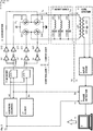
- Fig. 1a shows a first embodiment of an inventive metal detector 1 that comprises a transmitter unit 10 and a receiver unit 11 and a balanced coil system 6 with a drive coil L61 connected to the output of the transmitter unit 10 and two detection coils L62 and L63 connected on one end to ground potential and with the other end to an input stage 7 of the receiver unit 11.
- the input signal is typically amplified and filtered and then forwarded to a phase detector 8.
- the phase detector 8 allows distinguishing between the phases of the signal components of different origin and obtaining information about the observed product and contaminants, if present.
- a typical phase detector e.g.
- a frequency mixer or analogue multiplier circuit generates two independent voltage signals which represent the in-phase and quadrature component provided by the input stage 7, and a reference signal fm provided by the transmitter unit 10.
- the output signal of the phase detector 8 is further processed in a control unit 9, which is preferably equipped with a signal processor, input output devices, a keyboard and a display.
- the control unit 9 the user can control the operation of the metal detector 1.
- the user can select operating conditions of the metal detector, particularly the applied drive currents and operating frequencies as described below.
- the receiver unit 11 may include further features as generally known from conventional metal detectors.
- the transmitter unit 10 is a multi-frequency transmitter that is designed to provide a drive signal with a plurality of frequencies, e.g. two to eight frequencies, providing good sensitivity in a broad range of products and contaminants.
- the transmitter unit 10 comprises a drive controller 2, a drive unit 3, a converter 4 and preferably an admittance unit 5, which forwards a drive current i D provided by the converter 4 to the drive coil L61.
- the drive controller 2 comprises a memory unit 23 with one memory module 231 in which data that relates to the state of the drive switches S41, S42, S43, S44 for every clock cycle for a long period of the lowest operating frequency, e.g. switching angles ⁇ 1, ⁇ 2, ... of a pulse-width modulated signal or PXM-signal s PXM , are stored at related addresses. Determination of a pulse-width modulated signal s PXM is discussed below with reference to Fig. 4 . As outlined above, any pulse sequence PXM-signal s PXM that corresponds to the drive current when applied to the drive switches S41, S42, S43, S44 can be used.
- a pulse-width modulated signals or sequence or a pulse-density modulated signal or sequence is applied.
- PWM pulse-width modulated signals
- PDM pulse-density modulated signals
- PXM a modulated pulse sequence that corresponds to the drive current.
- the memory module 231 is sequentially addressed by the address counter 22 with address signal ad such that the data of the PXM-signal s PXM is sequentially read out of the memory module 231 and applied via the drive unit 3 to the drive switches S41, S42, S43, S44.
- the PXM-signal s PXM is routed via drive elements 31 and 311 to the input of drive switch S41, via drive elements 32 and 321 to the input of drive switch S42, via drive elements 31' and 312 to the input of drive switch S44 and via drive elements 32' and 322 to the input of drive switch S43.
- the drive elements 32 and 32' are inverters which ensure that the drive switches S42 and S43 always open, when the drive switches S41 and S44 are closed and that the drive switches S42 and S43 always closed, when the drive switches S41 and S44 are open. In this way an alternating current is flowing through the drive coil L61 while a short-circuit is avoided.
- the elements 31, 31' and 32, 32' have been duplicated.
- the output of element 31 could however be connected to the inputs of elements 311 and 312 and the output of element 32 could be connected to the inputs of elements 321 and 322 without requiring the elements 31' and 32'.
- a clock unit 21 which delivers reference signals fm to the address counter 22, the memory unit 23 and the phase detector 8.
- the drive switches S41, S42; S43, S44 are arranged in a full wave bridge circuit or H-bridge comprising a first branch and a second branch that are connected on one side to a drive voltage V D and on the other side to ground potential.
- the first branch comprises a first centre tap connected to the first end of the drive coil L61.
- the second branch comprises a second centre tap connected to the second end of the drive coil L61.
- a first pair of the drive switches S41, S42 is arranged in the first branch of the bridge and connected to one another at the first centre tap.
- a second pair of the drive switches S43, S44 is arranged in the second branch and connected to one another at the second centre tap.
- the PXM-signal s PXM this preferably created according to such a formula so that after conversion in the converter 4 a drive current i D e.g. with the four frequency components of this formula or a close approximation thereof is generated.
- Other harmonics are preferably avoided or suppressed.
- the desired harmonics are expanded.
- the admittance unit 5 comprises several branches, each provided with a capacitor C51; C52; C5n and an inductor L51; L52; L5n.
- the number n of branches corresponds to the number of frequency components present in the drive current i D .
- Each of the branches C51, L51; C52, L52; C5n, L5n forms together with the drive coil L61 a resonant circuit tuned to the corresponding frequency components ⁇ , 3 ⁇ , 7 ⁇ , 17 ⁇ of the drive current i D .
- the coil currents i L61 in the drive coil L61 at resonance are significantly larger than the drive current i D .
- the drive current i D flowing in the drive switches S41, S42; S43, S44 can be reduced, while high coil currents i L61 are reached.
- the converter 4 can therefore be dimensioned for lower currents and can be built at reduced costs.
- the metal detector of Fig. 1 a is tuned to a specific set of frequencies of the PXM-signal s PXM stored in the drive controller 2.
- the admittance unit 5 with its branches C51, L51; C52, L52; C5n, L5n is fixed to resonate together with the drive coil L61 at this set of frequency components ⁇ , 3 ⁇ , 7 ⁇ , 17 ⁇ .
- Fig. 1b shows the metal detector 1 of Fig. 1 a in an embodiment with a converter 4 with two drive switches S41, S42 that form a half-bridge and that are controlled by means of a selectable PXM-signal s PXM , such as a pulse-width or pulse-density modulated signal, provided by the drive controller 2.
- the drive switches S41, S42 provide a drive current i D via the admittance unit 5 to the drive coil L61.
- the drive switches S41, S42 form a half-bridge circuit that is connected on one side to a first voltage potential V D , e.g. the first drive voltage, and on the other side to a second voltage potential Vs, e.g. a second drive voltage.
- the drive switches S41, S42 are connected at a centre tap of the half-bridge circuit and are controlled such that the first end of the drive coil L61, which is connected to the centre tap, is alternately connected to the first voltage potential V D and to the second voltage potential V S .
- the PXM-signal s PXM can be generated online and forwarded to the converter 4.
- a selector switch S2 is provided, which is controlled by the control unit 9 by means of a control signal ctrl.
- the selector switch S2 can be set to receive a PXM-signal s PXM-STORED provided by the memory module 23 or to receive a PXM-signal s PXM-ONLINE provided online by a processor unit 25, e.g. a digital signal processer DSP, which is controlled by the control unit 9 by means of a control signal ctrl.
- processor unit 25 a program is implemented, with which suitable pulse-width modulated signals and/or pulse-density modulated signals can be generated.
- the processor unit 25, which, together with the other circuitry, is preferably integrated into the control unit 9, may also generate PXM-signals that are stored in the memory unit 23 for later use.
- the PXM-signal s PXM may be selected from the memory unit 23 and/or from the processor unit 25 with any configuration of drive switches S41, ..., S44 present and with any configuration of the admittance unit 5, if present.
- processor unit 25 can most advantageously be used to generate a PXM-signal s PXM online, with any set of operating frequencies.
- the admittance unit 5 may automatically be tuned to the same set of operating frequencies.
- the processor unit 25 may replace the memory unit 23 in all disclosed circuits or may be used as an alternative source for the PXM-signal s PXM .
- Fig. 2 shows the metal detector 1 of Fig. 1 a equipped with a drive controller 2, which provides a first PXM-signal s PXM1 used for controlling drive switches S41, S42 and a corresponding second PXM-signal s PXM2 used for controlling drive switches S43, S44.
- the first PXM-signal s PXM1 is stored in memory module 23A and the second PXM-signal s PXM2 stored in memory module 23B preferably at corresponding addresses.
- the address counter 22 can therefore synchronously address both memory modules 23A and 23B in order to simultaneously read out the first PXM-signal s PXM1 and the second PXM-signal s PXM2 .
- the memory modules 23A and 23B may store PXM-signals s PXM1 and s PXM2 that are inverted to one another. Having two PXM-signals makes it possible for the converter 4 to have 0 volts differential on its outputs when both PXM-signals are at ground potential or both are at the potential of the drive voltage V D . This allows the generation of trapezoidal waves and better current control.
- Fig. 3 shows the metal detector 1 of Fig. 1 a equipped with a drive controller 2 that allows selecting one of a plurality of stored PXM-signals s PXM , each provided with a specific set of frequency components, and with an admittance unit 5 that allows selectively connecting at least one of a plurality of branches, which preferably comprise each at least one capacitor C51; C52; C5n and at least one inductor L51; L52; L5n, to the drive coil L61 in order to create resonant circuits tuned to the frequency components of a selected PXM-signal s PXM .
- Data of each PXM-signal s PXM are stored individually in a corresponding memory module 231; 232; 23n.
- the branches of the admittance unit 5 can individually be activated by means of switches S51, S52, S5n which are actuated by means of a selector 50.
- control unit 9 provides a frequency select signal sf for example to the address counter 22, optionally to the memory unit 23, and to the selector 50.
- the address counter 22 will then address the selected memory module 231, 232 or 23n and the selector 50 the corresponding switches S51, S52, S5n.
- the metal detector 1 of Fig. 3 can therefore selectively be tuned to any set of frequencies selected for a specific product and potential contaminants.
- Resonance circuits can be tuned by adding capacitors and inductors e.g. by means of switches, such as electronic switches. Values of these items may also be changed electronically.
- the mathematically determined waveform of the drive current i( ⁇ t) is resembled or approximated by using triangular or trapezoidal segments.
- the mathematically determined waveform of the drive current i( ⁇ t) is shown in a dashed line.
- the waveform of the approximated triangular signal i DA closely follows the waveform of the mathematically determined drive current i( ⁇ t). In the first half of the period or the positive half wave, the maxima of the triangular signal i DA are set to the maxima of the mathematically determined drive current i( ⁇ t).
- the minima of the triangular signal i DA are set to the minima of the mathematically determined drive current i( ⁇ t).
- the approximated triangular signal i DA is not the actual drive current i D but ideally its mirror image.
- the approximated triangular signal i DA is converted to a PXM-signal s PXM , which is then converted in the converter 4 to the actual drive current i D , the mirror image of the approximated triangular signal i DA .
- the actual drive current i D at least approximately also corresponds to the approximated triangular signal i DA . If however, if higher frequencies are suppressed, then the virtual drive current i D will rather resemble the mathematically determined drive current i( ⁇ t).
- the switching angles ⁇ 1, ⁇ 2, ⁇ of the PXM-signal s PXM can be determined, which is required to control the drive switches S41, S42, S43, S44 in the converter 4.
- These switching angles ⁇ 1, ⁇ 2, ⁇ are positioned at the relative maxima and minima of the determined triangular signal i DA .
- the falling edges of the PXM-signal s PXM are set to occur at the maxima of the determined triangular signal i DA and the rising edges of the PXM-signal s PXM are set to occur at the minima of the determined triangular signal i DA .
- the obtained PXM-signal s PXM or PXM-signals s PXM1 , s PXM2 ,... is/are then stored in the memory unit 23, i.e. in one of the memory modules 231, 232, 23n; 23A, 23B.
- Fig. 4 shows the mathematically determined waveform of the drive current i( ⁇ t), the approximated triangular signal i DA and the determined PXM-signal s PXM for the length of one period of the lowest frequency ⁇ . Repetitively reading out the data of the PXM-signal s PXM from the related memory module 231, 232, 23n; 23A, 23B allows therefore to establish a continuous stream of the PXM-signal s PXM .
- Fig. 5 shows the coil current i L61 in the drive coil L61, the currents i L51 , i L52 in the branches of the admittance unit 5 (see Fig. 3 ) and the drive current i D delivered by the drive switches S41, S42, S43, S44 in the converter unit 4 for the complete frequency spectrum of the metal detectors of Fig. 1a , Fig. 1b , Fig. 2 and Fig. 3 .
- the curve of the drive current i D shows a strong decay at each resonant frequency frequencies f RES1 , f RES2 so that the drive current i D is well below the coil current i L61 at these positions of the spectrum.
- the power circulation at the predetermined drive frequencies f D1 , f D2 set to the resonant frequencies f RES1 , f RES2 is restricted within the loop formed by the admittance unit 5 and the drive coil L61 making the driving-point admittance to be zero on an ideal lossless system.
- the drive currents i D flowing at the drive frequencies f D1 , f D2 through the drive switches S41, S42, S43, S44 will be much lower than the coil currents i L61 flowing through the drive coil L61 and the branches of the admittance unit.
- MOSFETs typically MOSFETs
- admittance unit 5 In the drawings, preferred embodiments of the admittance unit 5 are shown. However, any other circuitry that preferably selectively allows reaching resonant circuits operating at defined frequencies f RES1 , f RES2 are of course also applicable.
Abstract
Description
- The current invention relates to a method for operating a multi-frequency metal detector and to a multi-frequency metal detector operating according to this method.
- As described in
US20120206138A1 , metal detectors are used to detect and reject unwanted metal contamination. When properly installed and operated, a metal detector will help reduce metal contamination and improving food safety. Most modern metal detectors utilise a search head comprising a coil system with a drive coil receiving a drive signal and generating an electromagnetic field in the product, and at least one detection coil arranged to detect fluctuations in the magnetic field caused by the presence of metallic particles in the product including ferrous, nonferrous and stainless steels in a large variety of products such as fresh and frozen food products. - A metal detection system that operates according to the "balanced coil"-principle typically comprises three coils, a drive coil and two identical detection coils that are wound onto a non-metallic frame, each exactly parallel with the other. Since the detection coils, which typically enclose the drive coil centred in between, are identical, an identical voltage is induced in each of them. In order to receive an output signal that is zero when the system is in balance, the first receiver coil is connected in series with the second receiver coil having an inversed sense of winding. Hence the voltages induced in the receiver coils, that are of identical amplitude and inverse polarity are cancelling out one another in the event that the system is in balance and no contamination is present in an observed product.
- However, as soon as a particle of metal passes through the coil arrangement, the electromagnetic field is disturbed first near one detection coil and then near the other detection coil. While the particle of metal is conveyed through the detection coils, the voltage induced in each detection coil is changed (by nano-volts). This change in balance results in a signal at the output of the detection coils that in a receiving unit can be processed, amplified and subsequently be used to detect the presence of the metal contamination in the observed product.
- In typical metal detectors, signal processing channels provided in the receiver unit split the received signal into two separate components that are 90° apart from one another. The resultant vector has a magnitude and a phase angle, which is typical for the products and the contaminants that are conveyed through the coil system. In order to identify a metal contaminant, "product effects" need to be removed or reduced. If the phase of the product is known then the corresponding signal vector can be reduced. Eliminating unwanted signals from the signal spectrum thus leads to higher sensitivity for signals originating from metal contaminants.
- Methods applied for eliminating unwanted signals from the signal spectrum therefore exploit the fact that metal contaminants, products and other disturbances have different influences on the magnetic field so that the resulting signals differ in phase. Signals caused by metals or products, as they pass through the coil system, can be split into two components, namely resistive and reactive components, according to conductivity and magnetic permeability of the measured object. Signals caused by ferrite are primarily reactive, while signals from stainless steel are primarily resistive. Products, which are conductive typically cause signals with a strong resistive component. Distinguishing between the phases of the signal components of different origin by means of a phase detector allows obtaining information about the product and the contaminants. Said signal components or phase and amplitude change depend on the frequency of the applied drive signal, which is selected such that the signal components of the metal contaminants will be out of phase with the signal components of the observed product signal.
-
US8473235 discloses a metal detector with a drive circuit that is connected to a drive coil and that comprises a plurality of switches driven by a drive controller, which alternately connect the drive coil across a potential difference to cause the drive coil to be driven at a predetermined operating frequency. The drive controller can be programmed to operate the plurality of switches to obtain any single operating frequency, which may be selectable in the range of 40 to 900 KHz in 1 Hz increments. However, driving the coil system by a square wave (or a trapezoidal wave due to the inductance of the coil) generates a large number of relatively high energy harmonics compared with the conventional sinusoidal signal generated by a tuned circuit. In order to avoid a negative impact of these harmonics, the apparatus comprises a detection circuit for deriving a signal from the coil system wherein the detection circuit comprises a phase sensitive detector coupled to a low pass filter that rejects said disturbing harmonics, which are generally regarded as most undesirable. - While one operating frequency may be suitable for one specific metal contaminant, the same frequency may not provide the desired results for other metal contaminants. Simultaneously using two or more transmitter frequencies selected according to product and potential contaminants allows obtaining more accurate information about two or more different metal contaminants without switching the operating frequency.
-
US8159225 discloses a multi-frequency metal detector with a multi-frequency transmitter and a method for generating a multi-frequency drive signal by generating at least two rectangular wave signals, each having a different fundamental frequency; mixing the selected rectangular wave signals to produce a switching signal containing different frequency components of relatively high magnitude, at frequencies corresponding to the convolution of the fundamental frequencies of the two selected rectangular wave signals. In addition to desired frequency components again other frequency components are present, which need to be removed or suppressed. -
US8159225 further discloses that the digital drive switching signal is applied to a full-bridge switching power stage connected to the drive coil of the metal detector. The full-bridge switching power stage consists of two half-bridges, each comprising two half-bridge switches, one half-bridge driven with the digital switching signal and the other half-bridge driven with the inverted digital switching signal. The current in the half-bridge switches of the full-bridge switching power stage corresponds to the current flowing in the drive coil. Hence, for high currents in the drive coil half-bridge switches, are required that are capable of delivering this high coil current. The multi-frequency transmitter must therefore be dimensioned and built accordingly with considerable costs. - The present invention is therefore based on the object of providing an improved method for operating a multi-frequency metal detector and to an improved multi-frequency metal detector operating according to this method.
- The inventive method and multi-frequency metal detector shall advantageously allow producing a multi-frequency drive signal with at least two different frequency components. Filtering circuitry shall be avoided or at least reduced.
- Further, the frequencies of the multi-frequency drive signals shall preferably be selectable as required so that the metal detector can flexibly be used for a wide range of products and potential contaminants.
- The metal detector shall be equipped with an improved multi-frequency transmitter that has improved efficiency, is constructively simple, can be built at reduced cost and allows maximising the coil current delivered to the drive coil.
- The inventive method and metal detector shall allow producing high drive currents in the drive coil, while currents in the transmitter unit remain comparably low so that the transmitter circuitry can be dimensioned accordingly, e.g. with reduced power performance and cost.
- In a first broad aspect of the invention there is provided a method for operating a metal detector, which comprises a drive coil designed for producing an electromagnetic field in a product, and at least one detection coil arranged for detecting fluctuations in the magnetic field caused by metallic particles present in the product, and a multi-frequency transmitter unit comprising a converter with a plurality of drive switches that are driven by a drive controller according to operating instructions such, that the drive switches alternately conduct a drive current through the drive coil so that the generated electromagnetic field exhibits two or more different frequency components.
- The electromagnetic field with the two or more different frequency components is reached by the steps of
- determining a waveform of the drive current for the at least two different frequency components;
- determining at least one pulse- sequence signal (below called PXM signal) corresponding to the defined waveform of the drive current;
- according to the operating instructions provided selecting the at least one determined PXM-signal which is determined online or stored in a memory module ; and
- generating and applying the determined PXM signal to control the drive switches of the transmitter unit, thereby generating the drive current with the defined waveform.
- The at least one PXM-signal, preferably a pulse-width modulated or pulse-density modulated signal, can be determined and then stored in memory for later use. However, preferably the PXM-signal is determined and generated online, so that the metal detector can be tuned online to products and contaminants or can be adapted online to changing products and contaminants. The user may therefore adjust the metal detector according to his personal requirements.
- Sarbari Das and Manish Bharat, Implementation of IGBT series resonant inverters using pulse-density modulation, International Journal of Industrial Electronics and Electrical Engineering, Volume-3, Issue-2, Feb. 2015, describe that pulse-density modulation is a form of modulation used to represent an analogue signal with digital data. In PDM, instead of specific amplitude values, the relative density of the pulses corresponds to the amplitude of the analogue signal.
- Pulse-width modulation techniques are described in M.J. Grimble, M.A. Johnson, Jian Sun, Advances in industrial Control, Springer-Verlag London Limited 2012, . In principle, a PWM signal can be produced by comparing a reference signal with a carrier signal, e.g. a sawtooth carrier, an inverted sawtooth carrier or a triangle carrier. The preferably mathematically determined waveform of the drive current can therefore be used as the reference signal which is compared with a carrier signal, e.g. a sawtooth or triangle carrier.
- The drive switches of the converter, preferably power-FET units, may be arranged for example as a bridge circuit or the half bridge circuit. In a first embodiment the drive switches are arranged as a full wave bridge or H-bridge comprising a first and a second branch that are connected on one side to a first voltage potential, e.g. a drive voltage, and on the other side to a second voltage potential, e.g. ground potential, and that comprise each a first or second centre tap, respectively, connected to a first or second end of the drive coil acting as a load. A first pair of the drive switches is arranged in the first branch and connected to one another at the first centre tap and a second pair of the drive switches is arranged in the second branch and connected to one another at the second centre tap. The drive switches are then controlled such that the first and second end of the drive coil are alternately connected to the first and the second voltage potential. I.e., the upper part of the first branch and the lower part of the second branch on the one hand and the lower part of the first branch and the upper part of the second branch on the other hand are activated alternatively thus leading an alternating current through the drive coil with the predetermined shape or waveform.
- In a second embodiment a first and a second drive switch form a half-bridge circuit that is connected on one side to a first voltage potential, e.g. a first drive voltage, and on the other side to a second voltage potential, e.g. a second drive voltage. The first and a second drive switch are connected at a centre tap of the half-bridge circuit and are controllable such that the first end of the drive coil, which is connected to the centre tap, is alternately connectable to the first voltage potential and to the second voltage potential.
- The drive switches are actuated by means of the predetermined PXM-signal or by two or more PXM signals. In the event that only one PXM-signal is provided, then this PXM signal is applied to the drive switches directly or via inverters, so that the individual drive switches are actuated correctly. In the event that two PXM signals are provided, the drive circuitry, which preferably comprises amplifiers, can get simplified.
- In a preferred embodiment the step of determining the shape or waveform of the drive current for two or more different frequency components comprises superposing current components individually relating to one of the at least two different frequency components. Such frequency components may be sinusoidal and may represent odd and/or even harmonics. Hence, the function of the drive current in the time domain can mathematically be determined, e.g. by a corresponding program module. The PXM-signals can be predetermined or can be determined, whenever the user selects new operating frequencies are frequency components.
- The user of the metal detector can therefore determine which frequencies or frequency components would be suitable for detecting potential contaminants or metal particles. The signal functions or drive current for each frequency component is then determined by superposition of each frequency component in the time domain. The fundamental angular frequency, i.e. the first frequency component is ω. In the formula below, the remaining angular frequencies are selected as the 3rd, 7th and 17th harmonics. The weights of the four angular frequency components have an inverse ratio in terms of the frequencies:

- The user of the metal detector can preferably determine any number of waveforms of the drive current for different sets of two or more different frequency components. For different products and/or different potential contaminants the user may therefore select the waveform of the drive current with the suitable set of frequency components. I.e., the user can continuously optimise detection processes.
- The PXM-signal corresponding to the preferably mathematically determined waveform of the drive current can be determined in various ways with a desired precision so that in the frequency domain only the desired frequency components appear. In the event that disturbing frequency components remain, such disturbing frequency components may be suppressed by a filter that is located before or after a phase detector, which receives a signal from the detection coils and a reference signal from the transmitter unit.
- In a preferred embodiment the pulse sequence or PXM-signal is obtained by approximating a triangular or trapezoidal signal to the preferably mathematically determined waveform of the drive current such that the maxima and minima of the determined waveform of the drive current and the maxima and minima of the triangular or trapezoidal signal correspond to one another and/or coincide. The switching angles for falling and rising edges of the PXM-signal are then sequentially defined at the maxima and minima of the triangular or trapezoidal signal. The approximation of the triangular or trapezoidal signal is preferably made in such a way that the minima or the maxima of the determined waveform of the drive current and the maxima or minima of the triangular or trapezoidal signal overlap at identical positions. The fundamental conception of this morphological approximation is that if two signals have similar time-domain waveforms, they shall share similar amplitude spectrum. Alternatively one of the PWM or PDM methods can be used to derive the pulse sequence signal.
- In a further preferred embodiment the described process for preferably mathematically determining the waveform of the drive current for the selected frequency components and for determining the corresponding PXM-signal is automatically executed by a processor and a corresponding program provided in the metal detector. The user of the metal detector can therefore freely select two or more suitable frequency components, whereafter said processor and program determine the PXM-signal or the related switching angles of the PXM-signal. Alternatively, switching angles for sets of standard operation frequencies can be firmly programmed and stored in the drive controller and selected according to the executed industrial or non-industrial processes.
- The waveform of the drive current with the embossed frequency components is preferably determined for one cycle duration of the frequency component with the lowest frequency present in the waveform of the drive current. This time segment of the drive current contains all information of the continuous drive current. The actual drive current can therefore be generated by sequentially repeating the preferably mathematically determined waveform of the drive current for the period of the lowest frequency contained in the drive current by the repeated application of the corresponding sequence of the PXM-signal.
- The drive current can directly be supplied to the drive coil so that's the drive current provided by the converter and the coil current delivered to the drive coil are identical. In a preferred embodiment however, the drive current it is supplied via an admittance unit to the drive coil, which admittance unit together with the drive coil forms resonant circuits that are active in the two or more different frequency components of the drive current. By tuning the resonant circuits of the admittance unit and the drive coil to the frequency components of the drive current or vice versa the current appearing in the drive coil will be significantly larger than the drive current flowing through the drive switches or power FETs. The multi-frequency transmitter unit with the power FETs can therefore be dimensioned for smaller currents than actually required in the drive coil. Furthermore when the output impedance of the converter is high by properly tuning the resonant circuits, the level of the frequency components desired for detecting contaminants in the products is increased, while other unwanted frequency components are not increased or even reduced, thus improving the signal-to-noise ratio of the obtained signals and the sensitivity of the metal detector.
- In a preferred embodiment the admittance unit comprises at least a first branch with a first capacitor and a first inductor that together with drive coil form a first resonant circuit and a second branch with a second capacitor and a second inductor that together with drive coil form a second resonant circuit. Preferably, the branches and/or the individual capacitors and inductors can be connected individually or in groups to the drive coil in order to establish the individual resonant circuits, which correspond to the frequency components embossed in the drive current.
- Most preferably, one of the stored PXM-signals with a specific set of frequency components and corresponding resonant circuits in the admittance unit are jointly selectable by the user of the metal detector. In this way the metal detector can instantaneously be optimised for any combination of products and contaminations.
- The implementation of the method and devices for creating the multi-frequency drive current on the one hand and the use of the admittance unit on the other hand are particularly advantageous when implemented in combination but also provide significant improvements, when implemented independently from one another. I.e., the inventive admittance unit which forms together with the drive coil two or more individually tuned resonant circuits can also advantageously be applied in metal detectors, in which the multi-frequency drive current these obtained according to another method.
- Detailed aspects and examples of the invention are described below with reference to the drawings, wherein
- Fig. 1a
- shows a an
inventive metal detector 1, which comprises aconverter 4 with four drive switches S41, S42, S43, S44 that for a bridge and that are controlled by means of a selectable pulse-width or pulse-density modulated signal sPXM, below called PXM-signal, provided by adrive controller 2 and that provide a drive current iD via anadmittance unit 5 to a drive coil L61; - Fig. 1b
- shows the
metal detector 1 ofFig. 1a , which comprises aconverter 4 with two drive switches S41, S42 that form a half-bridge and that are controlled by means of a selectable PXM-signal sPXM provided by thedrive controller 2 and that provide a drive current iD via theadmittance unit 5 to the drive coil L61; - Fig. 2
- shows the
metal detector 1 ofFig. 1 a equipped with adrive controller 2, which provides a first PXM-signal sPXM1 used for controlling drive switches S41, S42 and a corresponding second PXM-signal sPXM2 used for controlling drive switches S43, S44; - Fig. 3
- shows the
metal detector 1 ofFig. 1 a equipped with adrive controller 2 that allows selecting one of a plurality of stored PXM-signals sPXM, each provided with a specific set of frequency components, and with anadmittance unit 5 that allows selectively connecting at least one of a plurality of branches, which comprise each at least one capacitor C51; C52; C5n and at least one inductor L51; L52; L5n, to the drive coil L61 in order to create resonant circuits tuned to the frequency components of a selected PXM-signal sPXM; - Fig. 4
- shows a mathematically determined waveform of the drive current iD or i(ωt) that includes four frequency components ω, 3ω, 7ω and 17ω as well as the related PXM-signal sPXM determined by approximation of a triangular signal iDA to the determined waveform of the drive current i(ωt); and
- Fig. 5
- shows the coil current iL61 in the drive coil L61, the currents iL51, iL52 in the branches of the
admittance unit 5 and the drive current iD delivered by the drive switches S41, S42, S43, S44 in theconverter unit 4 for the complete frequency spectrum of the metal detectors ofFig. 1a ,Fig. 1b ,Fig. 2 andFig. 3 indicating that the drive current iD is significantly lower than the coil current iL61 if the frequency components fD1, fD2 of the drive current iD are set to the resonant frequencies fRES1, fRES2 of theadmittance circuit 5. -
Fig. 1a shows a first embodiment of aninventive metal detector 1 that comprises atransmitter unit 10 and areceiver unit 11 and abalanced coil system 6 with a drive coil L61 connected to the output of thetransmitter unit 10 and two detection coils L62 and L63 connected on one end to ground potential and with the other end to aninput stage 7 of thereceiver unit 11. In theinput stage 7 the input signal is typically amplified and filtered and then forwarded to aphase detector 8. Thephase detector 8 allows distinguishing between the phases of the signal components of different origin and obtaining information about the observed product and contaminants, if present. A typical phase detector, e.g. a frequency mixer or analogue multiplier circuit, generates two independent voltage signals which represent the in-phase and quadrature component provided by theinput stage 7, and a reference signal fm provided by thetransmitter unit 10. The output signal of thephase detector 8 is further processed in acontrol unit 9, which is preferably equipped with a signal processor, input output devices, a keyboard and a display. By means of thecontrol unit 9 the user can control the operation of themetal detector 1. In particular the user can select operating conditions of the metal detector, particularly the applied drive currents and operating frequencies as described below. Thereceiver unit 11 may include further features as generally known from conventional metal detectors. - The
transmitter unit 10 is a multi-frequency transmitter that is designed to provide a drive signal with a plurality of frequencies, e.g. two to eight frequencies, providing good sensitivity in a broad range of products and contaminants. Thetransmitter unit 10 comprises adrive controller 2, adrive unit 3, aconverter 4 and preferably anadmittance unit 5, which forwards a drive current iD provided by theconverter 4 to the drive coil L61. - In this embodiment of the invention the
drive controller 2 comprises amemory unit 23 with onememory module 231 in which data that relates to the state of the drive switches S41, S42, S43, S44 for every clock cycle for a long period of the lowest operating frequency, e.g. switching angles α1, α2, ... of a pulse-width modulated signal or PXM-signal sPXM, are stored at related addresses. Determination of a pulse-width modulated signal sPXM is discussed below with reference toFig. 4 . As outlined above, any pulse sequence PXM-signal sPXM that corresponds to the drive current when applied to the drive switches S41, S42, S43, S44 can be used. Preferably, a pulse-width modulated signals or sequence or a pulse-density modulated signal or sequence is applied. Hence, instead of using the acronym PWM for pulse-width modulated signals and PDM for pulse-density modulated signals, the acronym PXM is used, which stands for a modulated pulse sequence that corresponds to the drive current. - After the system has been reset by reset signal rs issued by the
control unit 9, thememory module 231 is sequentially addressed by theaddress counter 22 with address signal ad such that the data of the PXM-signal sPXM is sequentially read out of thememory module 231 and applied via thedrive unit 3 to the drive switches S41, S42, S43, S44. The PXM-signal sPXM is routed viadrive elements drive elements drive elements 31' and 312 to the input of drive switch S44 and viadrive elements 32' and 322 to the input of drive switch S43. Thedrive elements 32 and 32' are inverters which ensure that the drive switches S42 and S43 always open, when the drive switches S41 and S44 are closed and that the drive switches S42 and S43 always closed, when the drive switches S41 and S44 are open. In this way an alternating current is flowing through the drive coil L61 while a short-circuit is avoided. For the sake of simplicity of the drawing, theelements element 31 could however be connected to the inputs ofelements element 32 could be connected to the inputs ofelements - In order to obtain phase coherent operation of the metal detector a
clock unit 21 is provided, which delivers reference signals fm to theaddress counter 22, thememory unit 23 and thephase detector 8. - Since data of the PXM-signal sPXM are preferably stored for only one period of the lowest operating frequency, data are repetitively read out from the
memory module 231. The segment of the drive current iD shown inFig. 4 it is therefore sequentially and repetitively produced until the user terminates operation or changes settings. Theaddress counter 22 therefore counts from the lowest address number to the highest address number and restarts at the lowest address number. - The drive switches S41, S42; S43, S44 are arranged in a full wave bridge circuit or H-bridge comprising a first branch and a second branch that are connected on one side to a drive voltage VD and on the other side to ground potential. The first branch comprises a first centre tap connected to the first end of the drive coil L61. The second branch comprises a second centre tap connected to the second end of the drive coil L61. A first pair of the drive switches S41, S42 is arranged in the first branch of the bridge and connected to one another at the first centre tap. A second pair of the drive switches S43, S44 is arranged in the second branch and connected to one another at the second centre tap. As described above, by applying the PXM-signal sPXM to the drive switches S41, S42; S43, S44 the first and second end of the drive coil L61 are alternately connected to the drive voltage VD and ground potential, respectively.
- The
converter 4 converts the PXM-signal sPXM into a drive current iD which comprises desired frequency components, preferably harmonics of the lowest frequency, for example according to the formula, which has been used to determine the PXM-signal sPXM:
- As described below with reference to
Fig. 4 the PXM-signal sPXM this preferably created according to such a formula so that after conversion in the converter 4 a drive current iD e.g. with the four frequency components of this formula or a close approximation thereof is generated. Other harmonics are preferably avoided or suppressed. In order to increase sensitivity the desired harmonics are expanded. Further, it would be desirable to generate high coil currents iL61 with comparably small drive currents iD. These objects are reached by guiding the drive current iD via anadmittance unit 5 to the drive coil L61. - In the embodiment shown the
admittance unit 5 comprises several branches, each provided with a capacitor C51; C52; C5n and an inductor L51; L52; L5n. The number n of branches corresponds to the number of frequency components present in the drive current iD. Each of the branches C51, L51; C52, L52; C5n, L5n forms together with the drive coil L61 a resonant circuit tuned to the corresponding frequency components ω, 3ω, 7ω, 17ω of the drive current iD. The coil currents iL61 in the drive coil L61 at resonance are significantly larger than the drive current iD. Hence, on the one hand, the drive current iD flowing in the drive switches S41, S42; S43, S44 can be reduced, while high coil currents iL61 are reached. Theconverter 4 can therefore be dimensioned for lower currents and can be built at reduced costs. - The metal detector of
Fig. 1 a is tuned to a specific set of frequencies of the PXM-signal sPXM stored in thedrive controller 2. Theadmittance unit 5 with its branches C51, L51; C52, L52; C5n, L5n is fixed to resonate together with the drive coil L61 at this set of frequency components ω, 3ω, 7ω, 17ω. -
Fig. 1b shows themetal detector 1 ofFig. 1 a in an embodiment with aconverter 4 with two drive switches S41, S42 that form a half-bridge and that are controlled by means of a selectable PXM-signal sPXM, such as a pulse-width or pulse-density modulated signal, provided by thedrive controller 2. The drive switches S41, S42 provide a drive current iD via theadmittance unit 5 to the drive coil L61. The drive switches S41, S42 form a half-bridge circuit that is connected on one side to a first voltage potential VD, e.g. the first drive voltage, and on the other side to a second voltage potential Vs, e.g. a second drive voltage. The drive switches S41, S42 are connected at a centre tap of the half-bridge circuit and are controlled such that the first end of the drive coil L61, which is connected to the centre tap, is alternately connected to the first voltage potential VD and to the second voltage potential VS. - Further, as described above, in preferred embodiments, the PXM-signal sPXM can be generated online and forwarded to the
converter 4. InFig. 1b a selector switch S2 is provided, which is controlled by thecontrol unit 9 by means of a control signal ctrl. The selector switch S2 can be set to receive a PXM-signal sPXM-STORED provided by thememory module 23 or to receive a PXM-signal sPXM-ONLINE provided online by aprocessor unit 25, e.g. a digital signal processer DSP, which is controlled by thecontrol unit 9 by means of a control signal ctrl. In the processor unit 25 a program is implemented, with which suitable pulse-width modulated signals and/or pulse-density modulated signals can be generated. Theprocessor unit 25, which, together with the other circuitry, is preferably integrated into thecontrol unit 9, may also generate PXM-signals that are stored in thememory unit 23 for later use. - In all embodiments discussed, the PXM-signal sPXM may be selected from the
memory unit 23 and/or from theprocessor unit 25 with any configuration of drive switches S41, ..., S44 present and with any configuration of theadmittance unit 5, if present. Hence, the features of the individual embodiments can freely be combined. In particular,processor unit 25 can most advantageously be used to generate a PXM-signal sPXM online, with any set of operating frequencies. At the same time theadmittance unit 5 may automatically be tuned to the same set of operating frequencies. Theprocessor unit 25 may replace thememory unit 23 in all disclosed circuits or may be used as an alternative source for the PXM-signal sPXM. -
Fig. 2 shows themetal detector 1 ofFig. 1 a equipped with adrive controller 2, which provides a first PXM-signal sPXM1 used for controlling drive switches S41, S42 and a corresponding second PXM-signal sPXM2 used for controlling drive switches S43, S44. The first PXM-signal sPXM1 is stored inmemory module 23A and the second PXM-signal sPXM2 stored inmemory module 23B preferably at corresponding addresses. Theaddress counter 22 can therefore synchronously address bothmemory modules memory modules converter 4 to have 0 volts differential on its outputs when both PXM-signals are at ground potential or both are at the potential of the drive voltage VD. This allows the generation of trapezoidal waves and better current control. -
Fig. 3 shows themetal detector 1 ofFig. 1 a equipped with adrive controller 2 that allows selecting one of a plurality of stored PXM-signals sPXM, each provided with a specific set of frequency components, and with anadmittance unit 5 that allows selectively connecting at least one of a plurality of branches, which preferably comprise each at least one capacitor C51; C52; C5n and at least one inductor L51; L52; L5n, to the drive coil L61 in order to create resonant circuits tuned to the frequency components of a selected PXM-signal sPXM. Data of each PXM-signal sPXM are stored individually in acorresponding memory module 231; 232; 23n. The branches of theadmittance unit 5 can individually be activated by means of switches S51, S52, S5n which are actuated by means of aselector 50. - In order to select a specific PXM-signal sPXM with a desired set of operating frequencies ω1, ω2, ω3, ω4 and to select the corresponding resonant circuits or branches C51, L51; C52, L52; C5n, L5n in the
admittance unit 5, thecontrol unit 9 provides a frequency select signal sf for example to theaddress counter 22, optionally to thememory unit 23, and to theselector 50. Theaddress counter 22 will then address the selectedmemory module selector 50 the corresponding switches S51, S52, S5n. - The
metal detector 1 ofFig. 3 can therefore selectively be tuned to any set of frequencies selected for a specific product and potential contaminants. Resonance circuits can be tuned by adding capacitors and inductors e.g. by means of switches, such as electronic switches. Values of these items may also be changed electronically. -
Fig. 4 shows a mathematically determined waveform of the drive current i(ωt)
figure 1 and3 and three possible gradients including zero forfigure 2 , the mathematically determined waveform of the drive current i(ωt) is resembled or approximated by using triangular or trapezoidal segments. The mathematically determined waveform of the drive current i(ωt) is shown in a dashed line. The waveform of the approximated triangular signal iDA closely follows the waveform of the mathematically determined drive current i(ωt). In the first half of the period or the positive half wave, the maxima of the triangular signal iDA are set to the maxima of the mathematically determined drive current i(ωt). In the second half of the period or the negative half wave, the minima of the triangular signal iDA are set to the minima of the mathematically determined drive current i(ωt). The approximated triangular signal iDA is not the actual drive current iD but ideally its mirror image. The approximated triangular signal iDA is converted to a PXM-signal sPXM, which is then converted in theconverter 4 to the actual drive current iD, the mirror image of the approximated triangular signal iDA. InFig. 4 with brackets it is indicated that the actual drive current iD at least approximately also corresponds to the approximated triangular signal iDA. If however, if higher frequencies are suppressed, then the virtual drive current iD will rather resemble the mathematically determined drive current i(ωt). - Approximation by triangular or trapezoidal segments has the advantage that unwanted signals occur remote from the selected frequency components ω1, ω2, ω3, ω4 and therefore have no significant impact on measurement. Further the typical location of such disturbing signals in the Fourier spectrum is known, wherefore such disturbing signals can easily be suppressed in the
input stage 7 of thereceiver unit 11 by filter means selected accordingly.US8473235 mentioned above discloses a circuit with filter stages located subsequent to the phase detectors. In the present invention, filtering efforts are smaller. However any known filtering technique can also be applied to the signal delivered by the detection coils L62, L63 before or after demodulation, i.e. before and/or after thephase detector 8. - By means of the determined triangular signal iDA the switching angles α1, α2,··· of the PXM-signal sPXM can be determined, which is required to control the drive switches S41, S42, S43, S44 in the
converter 4. These switching angles α1, α2,··· are positioned at the relative maxima and minima of the determined triangular signal iDA. Thereby the falling edges of the PXM-signal sPXM are set to occur at the maxima of the determined triangular signal iDA and the rising edges of the PXM-signal sPXM are set to occur at the minima of the determined triangular signal iDA. The obtained PXM-signal sPXM or PXM-signals sPXM1, sPXM2,... is/are then stored in thememory unit 23, i.e. in one of thememory modules -
Fig. 4 shows the mathematically determined waveform of the drive current i(ωt), the approximated triangular signal iDA and the determined PXM-signal sPXM for the length of one period of the lowest frequency ω. Repetitively reading out the data of the PXM-signal sPXM from therelated memory module -
Fig. 5 shows the coil current iL61 in the drive coil L61, the currents iL51, iL52 in the branches of the admittance unit 5 (seeFig. 3 ) and the drive current iD delivered by the drive switches S41, S42, S43, S44 in theconverter unit 4 for the complete frequency spectrum of the metal detectors ofFig. 1a ,Fig. 1b ,Fig. 2 andFig. 3 . While the gradient of the coil current IL61 extends almost linear, the curve of the drive current iD shows a strong decay at each resonant frequency frequencies fRES1, fRES2 so that the drive current iD is well below the coil current iL61 at these positions of the spectrum. Hence, with comparably small drive currents iD with drive frequencies fD1, fD2 set to the resonant frequencies fRES1, fRES2 of theadmittance unit 5 and drive coil L61, or vice versa, large coil currents iL61 can be reached. An explanation for this advantageous effect can be given with regard to the currents iL51, iL52 appearing in the branches of theadmittance unit 5 which currents iL51, iL52, at the resonant frequencies fRES1, fRES2 of theadmittance unit 5, are equivalent to the coil current iL61 in the drive coil L61. Theadmittance unit 5 contains in its branches passive components, e.g. inductors L51; L52, L5n and capacitors C51, C52, C5n, which when in resonance together with the drive coil L61 cause the current to circulate between the drive coil L61 and the branches of theadmittance unit 5. Advantageously, the power circulation at the predetermined drive frequencies fD1, fD2 set to the resonant frequencies fRES1, fRES2 is restricted within the loop formed by theadmittance unit 5 and the drive coil L61 making the driving-point admittance to be zero on an ideal lossless system. Consequently, the drive currents iD flowing at the drive frequencies fD1, fD2 through the drive switches S41, S42, S43, S44 , typically MOSFETs, will be much lower than the coil currents iL61 flowing through the drive coil L61 and the branches of the admittance unit. Among other advantages, enables the extension of the spectrum towards lower frequencies and the possibility of driving a low impedance drive coil L61. - In the drawings, preferred embodiments of the
admittance unit 5 are shown. However, any other circuitry that preferably selectively allows reaching resonant circuits operating at defined frequencies fRES1, fRES2 are of course also applicable. -
- 1
- metal detector
- 10
- transmitter unit
- 11
- receiver unit
- 2
- drive controller
- S2
- selector switch
- 21
- clock unit
- 22
- address counter
- 23
- memory unit
- 23A, 23B
- memory modules
- 231, 232, 233
- memory modules
- 3
- drive unit
- 31, 31'
- drive elements
- 32, 32'
- inverting drive elements
- 311, 312, 321, 322
- amplifiers
- 4
- converter
- S41, S42, S43, S44
- drive switches
- 5
- admittance unit
- 50
- selector
- C51, C52, C53
- admittance capacitors
- L51, L52, L53
- admittance inductors
- S51, S52, S53
- admittance switches
- 6
- (balanced) coil system
- L61
- drive coil
- L62, L63
- detection coils
- 7
- input stage
- 8
- phase detector
- 9
- control unit / computer system
- ad
- address signal
- fm
- clock signal
- fD1, fD2
- frequency components
- iD
- drive current
- i(ωt)
- mathematically calculated drive current
- iDA
- approximated triangular signal
- iL51
- admittance current in inductor L51
- iL52
- admittance current in inductor L52
- iL61
- coil current
- rs
- reset signal
- sf
- frequency select signal
- sPXM
- pulse-width or pulse-density modulated signal
- VD
- first voltage potential, first drive voltage
- VS
- second voltage potential, second voltage
Claims (15)
- Method for operating a metal detector (1), which comprises a drive coil (L61) for producing an electromagnetic field in a product, and at least one detection coil (L62, L63) arranged to detect fluctuations in the magnetic field caused by metallic particles present in the product, and a multi-frequency transmitter unit (10) comprising a converter (4) with a plurality of drive switches (S41, S42; S43, S44) driven by a drive controller (2) according to operating instructions such, that the drive switches (S41, S42; S43, S44) alternately conduct a drive current (iD) through the drive coil (L61) so that the generated electromagnetic field exhibits two or more different frequency components (fD1, fD2); comprising the steps of:- determining a waveform of the drive current (iD) for the at least two different frequency components (fD1, fD2);- determining at least one PXM-signal (sPXM) that is a modulated pulse sequence, such as a pulse-width modulated or pulse-density modulated signal, and that corresponds to the determined waveform of the drive current (iD);- according to the operating instructions provided selecting the at least one determined PXM-signal (sPXM) which is determined online or stored in a memory module (231; 232); and- generating and applying the at least one determined PXM-signal (sPXM) to control the drive switches (S41, S42; S43, S44).
- Method for operating a metal detector (1) according to claim 1 wherein the step of determining the waveform of the drive current (iD) comprises superposing current components relating to the at least two different frequency components (fD1, fD2), such as sinusoidal frequency components (fD1, fD2) that are odd and/or even harmonics.
- Method for operating a metal detector (1) according to claim 1 or 2 comprising the step of determining the waveform of the drive current (iD) at least for a cycle duration of the frequency component (fD1) with the lowest frequency present in the drive current (iD) and generating the drive current (iD) by sequentially repeating the determined waveform of the drive current (iD).
- Method for operating a metal detector (1) according to claim 1, 2 or 3 comprising the steps of determining the PXM-signal (sPXM) by approximating a triangular or trapezoidal signal to the determined waveform of the drive current (iD) such that the maxima and minima of the determined waveform of the drive current (iD) and the maxima and minima of the triangular signal correspond to one another and/or coincide and defining switching angles (α1, α2, ...) sequentially for falling and rising edges of the PXM-signal (sPXM) at the maxima and minima of the triangular or trapezoidal signal.
- Method for operating a metal detector (1) according to one of the claims 1-4 comprising the steps of determining two or more PXM-signals (sPXM) each with different sets of frequency components (fD1; fD2) and storing the two or more PXM-signal (sPXM) in memory modules (231, 232), which are selectable for generating and applying one of the stored PXM-signal (sPXM).
- Method for operating a metal detector (1) according to one of the claims 1 - 5 comprising the steps of applying the PXM-signal (sPXM)- to a first and a second drive switch (S41, S42) of the drive switches (S41, S42; S43, S44), which form a half-bridge circuit that is connected on one side to a first voltage potential (VD) and on the other side to a second voltage potential (Vs), which are connected at a centre tap of the half-bridge circuit, and which are controlled such that the first end of the drive coil (L61), which is connected to the centre tap, is alternately connected to the first voltage potential (VD) and to the second voltage potential (VS), or- to the drive switches (S41, S42; S43, S44), which are arranged as a bridge circuit comprising a first and a second branch that are connected on one side to a first voltage potential (VD) and on the other side to a second voltage potential such as ground potential and that comprise each a first or second centre tap, respectively, connected to a first and second end of the drive coil (L61) with a first pair of the drive switches (S41, S42) arranged in the first branch and connected to one another at the first centre tap and with a second pair of the drive switches (S43, S44) arranged in the second branch and connected to one another at the second centre tap and which are controlled such that the first and second end of the drive coil (L61) are alternately connected to first voltage potential (VD) and to the second voltage potential.
- Method for operating a metal detector (1) according to one of the claims 1 - 5 comprising the steps of applying the PXM-signal (sPXM) via a drive unit (3) that comprises signal drive elements and/or inverters (31, 31', 32, 32', 311, 312, 321, 322) individually to control inputs of the drive switches (S41, S42; S43, S44).
- Method for operating a metal detector (1) according to one of the claims 1 - 7 comprising the steps of guiding the drive current (iD) directly or via an admittance unit (5) to the drive coil (L61), which admittance unit (5) together with the drive coil (L61) forms resonant circuits that are active in the two or more different frequency components (fD1, fD2) and in which resonant circuits the coil current (iL61) is larger than the drive current (iD).
- Method for operating a metal detector (1) according to claim 8 comprising the steps of using at least a first branch with a first capacitor (C51) and a first inductor (L51) in the admittance unit (5) that together with drive coil (L61) form the first resonant circuit and a second branch with a second capacitor (C52) and a second inductor (L52) in the admittance unit (5) that together with drive coil (L61) form the second resonant circuit.
- Method for operating a metal detector (1) according to claim 8 or 9 comprising the steps of selecting a PXM-signal (sPXM) with a set of frequency components (fD1; fD2) and activating resonant circuits in the admittance unit (5) that corresponds to the set of frequency components (fD1; fD2) of the selected PXM-signal (sPXM).
- Metal detector (1) operating according to a method as defined in one of the claims 1-10.
- Metal detector (1) according to claim 11 comprising a drive coil (L61) for producing an electromagnetic field in a product, and at least one detection coil (L62, L63) arranged to detect fluctuations in the magnetic field caused by metallic particles present in the product, and a multi-frequency transmitter unit (10) comprising a converter (4) with a plurality of drive switches (S41, S42; S43, S44) driven by a drive controller (2) according to operating instructions such, that the drive switches (S41, S42; S43, S44) alternately conduct a drive current (iD) through the drive coil (L61) so that the generated electromagnetic field exhibits two or more different frequency components (fD1, fD2); and with a memory unit (23) provided in the drive controller (2) in which data of at least one PXM-signal (sPXM) are stored that correspond to a waveform of the drive current (iD) determined for the two or more frequency components (fD1, fD2), which at least one PXM-signal (sPXM) is selectable to control the plurality of drive switches (S41, S42; S43, S44).
- Metal detector (1) according to claim 11 or 12 wherein
Method for operating a metal detector (1) according to one of the claims 1 - 5 comprising the steps of applying the PXM-signal (sPXM)- to a first and a second drive switch (S41, S42) of the drive switches (S41, S42; S43, S44), which form a half-bridge circuit that is connected on one side to a first voltage potential (VD) and on the other side to a second voltage potential (Vs), which are connected at a centre tap of the half-bridge circuit, and which are controllable such that the first end of the drive coil (L61), which is connected to the centre tap, is alternately connectable to the first voltage potential (VD) and to the second voltage potential (VS), or- to the drive switches (S41, S42; S43, S44), which are arranged as a bridge circuit comprising a first and a second branch that are connected on one side to a first voltage potential (VD) and on the other side to a second voltage potential such as ground potential and that comprise each a first or second centre tap, respectively, connected to a first and second end of the drive coil (L61) with a first pair of the drive switches (S41, S42) arranged in the first branch and connected to one another at the first centre tap and with a second pair of the drive switches (S43, S44) arranged in the second branch and connected to one another at the second centre tap and which are controllable such that the first and second end of the drive coil (L61) are alternately connectable to first voltage potential (VD) and to the second voltage potential. - Metal detector (1) according to claim 11, 12 or 13, wherein the converter (4) is connected directly or via an admittance unit (5) to the drive coil (L61), which admittance unit (5) together with the drive coil (L61) forms two or more resonant circuits each with a resonant frequency tuned at least approximately to one of the two or more different frequency components (fD1, fD2), said admittance unit (5) preferably comprising at least a first branch with a first capacitor (C51) and a first inductor (L51) in the admittance unit (5) that together with drive coil (L61) forms the first resonant circuit and a second branch with a second capacitor (C52) and a second inductor (L52) in the admittance unit (5) that together with drive coil (L61) forms the second resonant circuit.
- Metal detector (1) according to claim 14 wherein switching means (50, S51, S52) are provided which allow individually activating and deactivating resonant circuits in the admittance unit (5) in accordance with the selected.
Priority Applications (7)
| Application Number | Priority Date | Filing Date | Title |
|---|---|---|---|
| EP18154719.1A EP3521863A1 (en) | 2018-02-01 | 2018-02-01 | Method for operating a multi-frequency metal detector and multi-frequency metal detector |
| JP2018244700A JP2019132834A (en) | 2018-02-01 | 2018-12-27 | Method for operating multifrequency metal detector and multifrequency metal detector |
| BR102019001192-0A BR102019001192B1 (en) | 2018-02-01 | 2019-01-22 | METHOD FOR OPERATING A MULTIFREQUENCY METAL DETECTOR AND DEVICE FOR DETECTING METAL IN AN OBJECT BEING INSPECTED |
| CA3031774A CA3031774A1 (en) | 2018-02-01 | 2019-01-29 | Method for operating a multi-frequency metal detector and multi-frequency metal detector |
| US16/264,277 US10989829B2 (en) | 2018-02-01 | 2019-01-31 | Method for operating a multi-frequency metal detector and multi-frequency metal detector |
| CN201910104153.3A CN110161568B (en) | 2018-02-01 | 2019-02-01 | Method for operating a multi-frequency metal detector and multi-frequency metal detector |
| JP2023139636A JP2023159420A (en) | 2018-02-01 | 2023-08-30 | Method for operating multi-frequency metal detector and multi-frequency metal detector |
Applications Claiming Priority (1)
| Application Number | Priority Date | Filing Date | Title |
|---|---|---|---|
| EP18154719.1A EP3521863A1 (en) | 2018-02-01 | 2018-02-01 | Method for operating a multi-frequency metal detector and multi-frequency metal detector |
Publications (1)
| Publication Number | Publication Date |
|---|---|
| EP3521863A1 true EP3521863A1 (en) | 2019-08-07 |
Family
ID=61132320
Family Applications (1)
| Application Number | Title | Priority Date | Filing Date |
|---|---|---|---|
| EP18154719.1A Pending EP3521863A1 (en) | 2018-02-01 | 2018-02-01 | Method for operating a multi-frequency metal detector and multi-frequency metal detector |
Country Status (6)
| Country | Link |
|---|---|
| US (1) | US10989829B2 (en) |
| EP (1) | EP3521863A1 (en) |
| JP (2) | JP2019132834A (en) |
| CN (1) | CN110161568B (en) |
| BR (1) | BR102019001192B1 (en) |
| CA (1) | CA3031774A1 (en) |
Families Citing this family (2)
| Publication number | Priority date | Publication date | Assignee | Title |
|---|---|---|---|---|
| JP7456831B2 (en) * | 2019-04-17 | 2024-03-27 | メトラー-トレド・セーフライン・リミテッド | Methods for operating metal detectors and metal detectors |
| CN110726966B (en) * | 2019-12-03 | 2022-05-31 | 积成电子股份有限公司 | Device and method for monitoring whether non-contact electric energy meter has electricity or not |
Citations (8)
| Publication number | Priority date | Publication date | Assignee | Title |
|---|---|---|---|---|
| US6724191B1 (en) * | 2000-05-09 | 2004-04-20 | Admiralty Corporation | Systems and methods useful for detecting presence and/or location of various materials |
| US20050253711A1 (en) * | 2003-01-21 | 2005-11-17 | Nelson Carl V | Multi-mode electromagnetic target discriminator sensor system and method of operation thereof |
| US20080074114A1 (en) * | 2003-11-12 | 2008-03-27 | Bhc Consulting Pty. Ltd. | Multi-Frequency Metal Detector Having Constant Reactive Transmit Voltage Applied To A Transmit Coil |
| US8159225B2 (en) | 2008-06-23 | 2012-04-17 | Minelab Electronics Pty Ltd | Multi-frequency transmitter for a metal detector |
| US20120146647A1 (en) * | 2010-06-18 | 2012-06-14 | Minelab Electronics Pty Limited | Metal detector with at least one transmit/receive switch |
| US20120206138A1 (en) | 2010-10-07 | 2012-08-16 | Mettler-Toledo Safeline Limited | Method for operating a metal detection system and metal detection system |
| EP2570824A1 (en) * | 2011-09-19 | 2013-03-20 | Mettler-Toledo Safeline Limited | Method for operating a metal detection apparatus and apparatus |
| US8473235B2 (en) | 2005-02-16 | 2013-06-25 | Illinois Tool Works Inc. | Metal detector |
Family Cites Families (12)
| Publication number | Priority date | Publication date | Assignee | Title |
|---|---|---|---|---|
| WO2006037176A1 (en) * | 2004-10-06 | 2006-04-13 | Kenneth Brian Roberts | Multi coil metal detector |
| JP2007278719A (en) * | 2006-04-03 | 2007-10-25 | Nec Tokin Corp | Metal detector |
| EP2439559B1 (en) * | 2010-10-07 | 2013-05-29 | Mettler-Toledo Safeline Limited | Method for operating of a metal detection system and metal detection system |
| US9606084B2 (en) * | 2011-02-02 | 2017-03-28 | Gerd Reime | Metal detector for locating metal objects |
| EP2562565B1 (en) * | 2011-08-24 | 2014-03-05 | Mettler-Toledo Safeline Limited | Metal Detection Apparatus |
| US9018935B2 (en) * | 2011-09-19 | 2015-04-28 | Mettler-Toledo Safeline Limited | Method for operating a metal detection apparatus and apparatus |
| BR112014019417B1 (en) * | 2012-02-10 | 2022-06-28 | Illinois Tool Works Inc | METHOD OF BALANCING AN OUTPUT SIGNAL OF A VARIABLE FREQUENCY METAL DETECTOR AND METAL DETECTOR |
| GB2499239B (en) * | 2012-02-10 | 2014-02-12 | Illinois Tool Works | Metal detector |
| CN108173350B (en) * | 2012-05-02 | 2021-06-15 | 苹果公司 | Inductive power transmitter and method for detecting and identifying receiver |
| EP2924472B1 (en) * | 2014-03-25 | 2020-01-15 | Mettler-Toledo Safeline Limited | Method for monitoring the operation of a metal detection system and metal detection system |
| EP3182169B1 (en) * | 2015-12-17 | 2018-12-05 | Mettler-Toledo Safeline Limited | Metal detection apparatus |
| CN107422029B (en) * | 2017-04-28 | 2020-11-03 | 陕西科技大学 | Device and method for accurately detecting defects of metal plate |
-
2018
- 2018-02-01 EP EP18154719.1A patent/EP3521863A1/en active Pending
- 2018-12-27 JP JP2018244700A patent/JP2019132834A/en active Pending
-
2019
- 2019-01-22 BR BR102019001192-0A patent/BR102019001192B1/en active IP Right Grant
- 2019-01-29 CA CA3031774A patent/CA3031774A1/en active Pending
- 2019-01-31 US US16/264,277 patent/US10989829B2/en active Active
- 2019-02-01 CN CN201910104153.3A patent/CN110161568B/en active Active
-
2023
- 2023-08-30 JP JP2023139636A patent/JP2023159420A/en active Pending
Patent Citations (8)
| Publication number | Priority date | Publication date | Assignee | Title |
|---|---|---|---|---|
| US6724191B1 (en) * | 2000-05-09 | 2004-04-20 | Admiralty Corporation | Systems and methods useful for detecting presence and/or location of various materials |
| US20050253711A1 (en) * | 2003-01-21 | 2005-11-17 | Nelson Carl V | Multi-mode electromagnetic target discriminator sensor system and method of operation thereof |
| US20080074114A1 (en) * | 2003-11-12 | 2008-03-27 | Bhc Consulting Pty. Ltd. | Multi-Frequency Metal Detector Having Constant Reactive Transmit Voltage Applied To A Transmit Coil |
| US8473235B2 (en) | 2005-02-16 | 2013-06-25 | Illinois Tool Works Inc. | Metal detector |
| US8159225B2 (en) | 2008-06-23 | 2012-04-17 | Minelab Electronics Pty Ltd | Multi-frequency transmitter for a metal detector |
| US20120146647A1 (en) * | 2010-06-18 | 2012-06-14 | Minelab Electronics Pty Limited | Metal detector with at least one transmit/receive switch |
| US20120206138A1 (en) | 2010-10-07 | 2012-08-16 | Mettler-Toledo Safeline Limited | Method for operating a metal detection system and metal detection system |
| EP2570824A1 (en) * | 2011-09-19 | 2013-03-20 | Mettler-Toledo Safeline Limited | Method for operating a metal detection apparatus and apparatus |
Non-Patent Citations (2)
| Title |
|---|
| M.J. GRIMBLE; M.A. JOHNSON; JIAN SUN: "Advances in industrial Control", 2012, SPRINGER-VERLAG LONDON LIMITED |
| SARBARI DAS; MANISH BHARAT: "Implementation of IGBT series resonant inverters using pulse-density modulation", INTERNATIONAL JOURNAL OF INDUSTRIAL ELECTRONICS AND ELECTRICAL ENGINEERING, vol. 3, no. 2, February 2015 (2015-02-01) |
Also Published As
| Publication number | Publication date |
|---|---|
| CN110161568B (en) | 2024-01-09 |
| BR102019001192A2 (en) | 2019-08-20 |
| BR102019001192B1 (en) | 2023-10-24 |
| JP2019132834A (en) | 2019-08-08 |
| CA3031774A1 (en) | 2019-08-01 |
| US10989829B2 (en) | 2021-04-27 |
| CN110161568A (en) | 2019-08-23 |
| US20190235118A1 (en) | 2019-08-01 |
| JP2023159420A (en) | 2023-10-31 |
| BR102019001192A8 (en) | 2023-03-28 |
Similar Documents
| Publication | Publication Date | Title |
|---|---|---|
| JP2023159420A (en) | Method for operating multi-frequency metal detector and multi-frequency metal detector | |
| JP5952677B2 (en) | Metal detector | |
| EP0608966B1 (en) | Adjustable reactance device and method | |
| US8159225B2 (en) | Multi-frequency transmitter for a metal detector | |
| US9018935B2 (en) | Method for operating a metal detection apparatus and apparatus | |
| US11022712B2 (en) | Multi-frequency metal detector | |
| JP7469939B2 (en) | METHOD FOR OPERATING A METAL DETECTOR AND METAL DETECTOR - Patent application | |
| EP2570824B1 (en) | Method for operating a metal detection apparatus and apparatus | |
| JPS6341502B2 (en) | ||
| US5877706A (en) | Ferromagnetic object detector | |
| US5325060A (en) | Coil circuits | |
| KR900010407A (en) | Lead free frequency detector of electrical signal | |
| US7683709B1 (en) | Low frequency power amplifier employing high frequency magnetic components | |
| JP2005094913A (en) | Phase shift type high-frequency inverter device | |
| SU1188630A1 (en) | Method of non-contact multiparameter inspection of articles from electro-conducting materials | |
| WO1994006029A1 (en) | Method of measuring magnetic field induction | |
| SU1529098A1 (en) | Electromagnetic and acoustic method of non-destructive check of defects in articles from ferromagnetic materials and device for effecting same | |
| SU824088A1 (en) | Device for oscillography of complex reversal of ferromagnet magnetization dynamics | |
| CA2159259C (en) | Multifrequency electromagnetic surveying method and system | |
| SU1068800A1 (en) | Two-frequency flaw detector (its versions) | |
| SU577468A1 (en) | Frequency sensor | |
| SU843148A1 (en) | Generator of hign-frequency unipolar current pulses | |
| RU2331113C2 (en) | Device for detection and classification of metal objects | |
| CN1161596A (en) | Electric power conversion circuit by changing sine ac power to balance amplitude-modulated wave |
Legal Events
| Date | Code | Title | Description |
|---|---|---|---|
| PUAI | Public reference made under article 153(3) epc to a published international application that has entered the european phase |
Free format text: ORIGINAL CODE: 0009012 |
|
| STAA | Information on the status of an ep patent application or granted ep patent |
Free format text: STATUS: THE APPLICATION HAS BEEN PUBLISHED |
|
| AK | Designated contracting states |
Kind code of ref document: A1 Designated state(s): AL AT BE BG CH CY CZ DE DK EE ES FI FR GB GR HR HU IE IS IT LI LT LU LV MC MK MT NL NO PL PT RO RS SE SI SK SM TR |
|
| AX | Request for extension of the european patent |
Extension state: BA ME |
|
| STAA | Information on the status of an ep patent application or granted ep patent |
Free format text: STATUS: REQUEST FOR EXAMINATION WAS MADE |
|
| 17P | Request for examination filed |
Effective date: 20191220 |
|
| RBV | Designated contracting states (corrected) |
Designated state(s): AL AT BE BG CH CY CZ DE DK EE ES FI FR GB GR HR HU IE IS IT LI LT LU LV MC MK MT NL NO PL PT RO RS SE SI SK SM TR |
|
| STAA | Information on the status of an ep patent application or granted ep patent |
Free format text: STATUS: EXAMINATION IS IN PROGRESS |
|
| 17Q | First examination report despatched |
Effective date: 20220331 |
|
| GRAP | Despatch of communication of intention to grant a patent |
Free format text: ORIGINAL CODE: EPIDOSNIGR1 |
|
| STAA | Information on the status of an ep patent application or granted ep patent |
Free format text: STATUS: GRANT OF PATENT IS INTENDED |