EP3521264A1 - Silicon carbide member for plasma treatment apparatus, and method of manufacturing same - Google Patents
Silicon carbide member for plasma treatment apparatus, and method of manufacturing same Download PDFInfo
- Publication number
- EP3521264A1 EP3521264A1 EP17855734.4A EP17855734A EP3521264A1 EP 3521264 A1 EP3521264 A1 EP 3521264A1 EP 17855734 A EP17855734 A EP 17855734A EP 3521264 A1 EP3521264 A1 EP 3521264A1
- Authority
- EP
- European Patent Office
- Prior art keywords
- silicon carbide
- amount
- sic
- ppm
- sintering aid
- Prior art date
- Legal status (The legal status is an assumption and is not a legal conclusion. Google has not performed a legal analysis and makes no representation as to the accuracy of the status listed.)
- Granted
Links
Images


Classifications
-
- C—CHEMISTRY; METALLURGY
- C04—CEMENTS; CONCRETE; ARTIFICIAL STONE; CERAMICS; REFRACTORIES
- C04B—LIME, MAGNESIA; SLAG; CEMENTS; COMPOSITIONS THEREOF, e.g. MORTARS, CONCRETE OR LIKE BUILDING MATERIALS; ARTIFICIAL STONE; CERAMICS; REFRACTORIES; TREATMENT OF NATURAL STONE
- C04B35/00—Shaped ceramic products characterised by their composition; Ceramics compositions; Processing powders of inorganic compounds preparatory to the manufacturing of ceramic products
- C04B35/515—Shaped ceramic products characterised by their composition; Ceramics compositions; Processing powders of inorganic compounds preparatory to the manufacturing of ceramic products based on non-oxide ceramics
- C04B35/56—Shaped ceramic products characterised by their composition; Ceramics compositions; Processing powders of inorganic compounds preparatory to the manufacturing of ceramic products based on non-oxide ceramics based on carbides or oxycarbides
- C04B35/565—Shaped ceramic products characterised by their composition; Ceramics compositions; Processing powders of inorganic compounds preparatory to the manufacturing of ceramic products based on non-oxide ceramics based on carbides or oxycarbides based on silicon carbide
- C04B35/575—Shaped ceramic products characterised by their composition; Ceramics compositions; Processing powders of inorganic compounds preparatory to the manufacturing of ceramic products based on non-oxide ceramics based on carbides or oxycarbides based on silicon carbide obtained by pressure sintering
-
- C—CHEMISTRY; METALLURGY
- C04—CEMENTS; CONCRETE; ARTIFICIAL STONE; CERAMICS; REFRACTORIES
- C04B—LIME, MAGNESIA; SLAG; CEMENTS; COMPOSITIONS THEREOF, e.g. MORTARS, CONCRETE OR LIKE BUILDING MATERIALS; ARTIFICIAL STONE; CERAMICS; REFRACTORIES; TREATMENT OF NATURAL STONE
- C04B35/00—Shaped ceramic products characterised by their composition; Ceramics compositions; Processing powders of inorganic compounds preparatory to the manufacturing of ceramic products
- C04B35/622—Forming processes; Processing powders of inorganic compounds preparatory to the manufacturing of ceramic products
- C04B35/626—Preparing or treating the powders individually or as batches ; preparing or treating macroscopic reinforcing agents for ceramic products, e.g. fibres; mechanical aspects section B
- C04B35/62605—Treating the starting powders individually or as mixtures
- C04B35/6261—Milling
-
- C—CHEMISTRY; METALLURGY
- C04—CEMENTS; CONCRETE; ARTIFICIAL STONE; CERAMICS; REFRACTORIES
- C04B—LIME, MAGNESIA; SLAG; CEMENTS; COMPOSITIONS THEREOF, e.g. MORTARS, CONCRETE OR LIKE BUILDING MATERIALS; ARTIFICIAL STONE; CERAMICS; REFRACTORIES; TREATMENT OF NATURAL STONE
- C04B35/00—Shaped ceramic products characterised by their composition; Ceramics compositions; Processing powders of inorganic compounds preparatory to the manufacturing of ceramic products
- C04B35/622—Forming processes; Processing powders of inorganic compounds preparatory to the manufacturing of ceramic products
- C04B35/626—Preparing or treating the powders individually or as batches ; preparing or treating macroscopic reinforcing agents for ceramic products, e.g. fibres; mechanical aspects section B
- C04B35/62605—Treating the starting powders individually or as mixtures
- C04B35/62625—Wet mixtures
- C04B35/6263—Wet mixtures characterised by their solids loadings, i.e. the percentage of solids
-
- C—CHEMISTRY; METALLURGY
- C04—CEMENTS; CONCRETE; ARTIFICIAL STONE; CERAMICS; REFRACTORIES
- C04B—LIME, MAGNESIA; SLAG; CEMENTS; COMPOSITIONS THEREOF, e.g. MORTARS, CONCRETE OR LIKE BUILDING MATERIALS; ARTIFICIAL STONE; CERAMICS; REFRACTORIES; TREATMENT OF NATURAL STONE
- C04B35/00—Shaped ceramic products characterised by their composition; Ceramics compositions; Processing powders of inorganic compounds preparatory to the manufacturing of ceramic products
- C04B35/622—Forming processes; Processing powders of inorganic compounds preparatory to the manufacturing of ceramic products
- C04B35/626—Preparing or treating the powders individually or as batches ; preparing or treating macroscopic reinforcing agents for ceramic products, e.g. fibres; mechanical aspects section B
- C04B35/62605—Treating the starting powders individually or as mixtures
- C04B35/62625—Wet mixtures
- C04B35/6264—Mixing media, e.g. organic solvents
-
- C—CHEMISTRY; METALLURGY
- C04—CEMENTS; CONCRETE; ARTIFICIAL STONE; CERAMICS; REFRACTORIES
- C04B—LIME, MAGNESIA; SLAG; CEMENTS; COMPOSITIONS THEREOF, e.g. MORTARS, CONCRETE OR LIKE BUILDING MATERIALS; ARTIFICIAL STONE; CERAMICS; REFRACTORIES; TREATMENT OF NATURAL STONE
- C04B35/00—Shaped ceramic products characterised by their composition; Ceramics compositions; Processing powders of inorganic compounds preparatory to the manufacturing of ceramic products
- C04B35/622—Forming processes; Processing powders of inorganic compounds preparatory to the manufacturing of ceramic products
- C04B35/626—Preparing or treating the powders individually or as batches ; preparing or treating macroscopic reinforcing agents for ceramic products, e.g. fibres; mechanical aspects section B
- C04B35/62605—Treating the starting powders individually or as mixtures
- C04B35/62645—Thermal treatment of powders or mixtures thereof other than sintering
- C04B35/62655—Drying, e.g. freeze-drying, spray-drying, microwave or supercritical drying
-
- C—CHEMISTRY; METALLURGY
- C04—CEMENTS; CONCRETE; ARTIFICIAL STONE; CERAMICS; REFRACTORIES
- C04B—LIME, MAGNESIA; SLAG; CEMENTS; COMPOSITIONS THEREOF, e.g. MORTARS, CONCRETE OR LIKE BUILDING MATERIALS; ARTIFICIAL STONE; CERAMICS; REFRACTORIES; TREATMENT OF NATURAL STONE
- C04B35/00—Shaped ceramic products characterised by their composition; Ceramics compositions; Processing powders of inorganic compounds preparatory to the manufacturing of ceramic products
- C04B35/622—Forming processes; Processing powders of inorganic compounds preparatory to the manufacturing of ceramic products
- C04B35/64—Burning or sintering processes
- C04B35/645—Pressure sintering
-
- C—CHEMISTRY; METALLURGY
- C23—COATING METALLIC MATERIAL; COATING MATERIAL WITH METALLIC MATERIAL; CHEMICAL SURFACE TREATMENT; DIFFUSION TREATMENT OF METALLIC MATERIAL; COATING BY VACUUM EVAPORATION, BY SPUTTERING, BY ION IMPLANTATION OR BY CHEMICAL VAPOUR DEPOSITION, IN GENERAL; INHIBITING CORROSION OF METALLIC MATERIAL OR INCRUSTATION IN GENERAL
- C23C—COATING METALLIC MATERIAL; COATING MATERIAL WITH METALLIC MATERIAL; SURFACE TREATMENT OF METALLIC MATERIAL BY DIFFUSION INTO THE SURFACE, BY CHEMICAL CONVERSION OR SUBSTITUTION; COATING BY VACUUM EVAPORATION, BY SPUTTERING, BY ION IMPLANTATION OR BY CHEMICAL VAPOUR DEPOSITION, IN GENERAL
- C23C16/00—Chemical coating by decomposition of gaseous compounds, without leaving reaction products of surface material in the coating, i.e. chemical vapour deposition [CVD] processes
- C23C16/22—Chemical coating by decomposition of gaseous compounds, without leaving reaction products of surface material in the coating, i.e. chemical vapour deposition [CVD] processes characterised by the deposition of inorganic material, other than metallic material
- C23C16/30—Deposition of compounds, mixtures or solid solutions, e.g. borides, carbides, nitrides
- C23C16/32—Carbides
- C23C16/325—Silicon carbide
-
- H—ELECTRICITY
- H01—ELECTRIC ELEMENTS
- H01J—ELECTRIC DISCHARGE TUBES OR DISCHARGE LAMPS
- H01J37/00—Discharge tubes with provision for introducing objects or material to be exposed to the discharge, e.g. for the purpose of examination or processing thereof
- H01J37/32—Gas-filled discharge tubes
- H01J37/32431—Constructional details of the reactor
- H01J37/3244—Gas supply means
-
- H—ELECTRICITY
- H01—ELECTRIC ELEMENTS
- H01J—ELECTRIC DISCHARGE TUBES OR DISCHARGE LAMPS
- H01J37/00—Discharge tubes with provision for introducing objects or material to be exposed to the discharge, e.g. for the purpose of examination or processing thereof
- H01J37/32—Gas-filled discharge tubes
- H01J37/32431—Constructional details of the reactor
- H01J37/32458—Vessel
- H01J37/32467—Material
-
- H—ELECTRICITY
- H01—ELECTRIC ELEMENTS
- H01J—ELECTRIC DISCHARGE TUBES OR DISCHARGE LAMPS
- H01J37/00—Discharge tubes with provision for introducing objects or material to be exposed to the discharge, e.g. for the purpose of examination or processing thereof
- H01J37/32—Gas-filled discharge tubes
- H01J37/32431—Constructional details of the reactor
- H01J37/32458—Vessel
- H01J37/32477—Vessel characterised by the means for protecting vessels or internal parts, e.g. coatings
- H01J37/32495—Means for protecting the vessel against plasma
-
- H—ELECTRICITY
- H01—ELECTRIC ELEMENTS
- H01J—ELECTRIC DISCHARGE TUBES OR DISCHARGE LAMPS
- H01J37/00—Discharge tubes with provision for introducing objects or material to be exposed to the discharge, e.g. for the purpose of examination or processing thereof
- H01J37/32—Gas-filled discharge tubes
- H01J37/32431—Constructional details of the reactor
- H01J37/32623—Mechanical discharge control means
- H01J37/32642—Focus rings
-
- H—ELECTRICITY
- H10—SEMICONDUCTOR DEVICES; ELECTRIC SOLID-STATE DEVICES NOT OTHERWISE PROVIDED FOR
- H10P—GENERIC PROCESSES OR APPARATUS FOR THE MANUFACTURE OR TREATMENT OF DEVICES COVERED BY CLASS H10
- H10P50/00—Etching of wafers, substrates or parts of devices
- H10P50/20—Dry etching; Plasma etching; Reactive-ion etching
- H10P50/24—Dry etching; Plasma etching; Reactive-ion etching of semiconductor materials
- H10P50/242—Dry etching; Plasma etching; Reactive-ion etching of semiconductor materials of Group IV materials
-
- H—ELECTRICITY
- H10—SEMICONDUCTOR DEVICES; ELECTRIC SOLID-STATE DEVICES NOT OTHERWISE PROVIDED FOR
- H10P—GENERIC PROCESSES OR APPARATUS FOR THE MANUFACTURE OR TREATMENT OF DEVICES COVERED BY CLASS H10
- H10P72/00—Handling or holding of wafers, substrates or devices during manufacture or treatment thereof
- H10P72/70—Handling or holding of wafers, substrates or devices during manufacture or treatment thereof for supporting or gripping
- H10P72/76—Handling or holding of wafers, substrates or devices during manufacture or treatment thereof for supporting or gripping using mechanical means, e.g. clamps or pinches
- H10P72/7604—Handling or holding of wafers, substrates or devices during manufacture or treatment thereof for supporting or gripping using mechanical means, e.g. clamps or pinches the wafers being placed on a susceptor, stage or support
- H10P72/7611—Handling or holding of wafers, substrates or devices during manufacture or treatment thereof for supporting or gripping using mechanical means, e.g. clamps or pinches the wafers being placed on a susceptor, stage or support characterised by edge profile or support profile
-
- H—ELECTRICITY
- H10—SEMICONDUCTOR DEVICES; ELECTRIC SOLID-STATE DEVICES NOT OTHERWISE PROVIDED FOR
- H10P—GENERIC PROCESSES OR APPARATUS FOR THE MANUFACTURE OR TREATMENT OF DEVICES COVERED BY CLASS H10
- H10P72/00—Handling or holding of wafers, substrates or devices during manufacture or treatment thereof
- H10P72/70—Handling or holding of wafers, substrates or devices during manufacture or treatment thereof for supporting or gripping
- H10P72/76—Handling or holding of wafers, substrates or devices during manufacture or treatment thereof for supporting or gripping using mechanical means, e.g. clamps or pinches
- H10P72/7604—Handling or holding of wafers, substrates or devices during manufacture or treatment thereof for supporting or gripping using mechanical means, e.g. clamps or pinches the wafers being placed on a susceptor, stage or support
- H10P72/7616—Handling or holding of wafers, substrates or devices during manufacture or treatment thereof for supporting or gripping using mechanical means, e.g. clamps or pinches the wafers being placed on a susceptor, stage or support characterised by a coating, a hardness or a material
-
- C—CHEMISTRY; METALLURGY
- C04—CEMENTS; CONCRETE; ARTIFICIAL STONE; CERAMICS; REFRACTORIES
- C04B—LIME, MAGNESIA; SLAG; CEMENTS; COMPOSITIONS THEREOF, e.g. MORTARS, CONCRETE OR LIKE BUILDING MATERIALS; ARTIFICIAL STONE; CERAMICS; REFRACTORIES; TREATMENT OF NATURAL STONE
- C04B2235/00—Aspects relating to ceramic starting mixtures or sintered ceramic products
- C04B2235/02—Composition of constituents of the starting material or of secondary phases of the final product
- C04B2235/30—Constituents and secondary phases not being of a fibrous nature
- C04B2235/32—Metal oxides, mixed metal oxides, or oxide-forming salts thereof, e.g. carbonates, nitrates, (oxy)hydroxides, chlorides
- C04B2235/3217—Aluminum oxide or oxide forming salts thereof, e.g. bauxite, alpha-alumina
-
- C—CHEMISTRY; METALLURGY
- C04—CEMENTS; CONCRETE; ARTIFICIAL STONE; CERAMICS; REFRACTORIES
- C04B—LIME, MAGNESIA; SLAG; CEMENTS; COMPOSITIONS THEREOF, e.g. MORTARS, CONCRETE OR LIKE BUILDING MATERIALS; ARTIFICIAL STONE; CERAMICS; REFRACTORIES; TREATMENT OF NATURAL STONE
- C04B2235/00—Aspects relating to ceramic starting mixtures or sintered ceramic products
- C04B2235/02—Composition of constituents of the starting material or of secondary phases of the final product
- C04B2235/30—Constituents and secondary phases not being of a fibrous nature
- C04B2235/32—Metal oxides, mixed metal oxides, or oxide-forming salts thereof, e.g. carbonates, nitrates, (oxy)hydroxides, chlorides
- C04B2235/3224—Rare earth oxide or oxide forming salts thereof, e.g. scandium oxide
- C04B2235/3225—Yttrium oxide or oxide-forming salts thereof
-
- C—CHEMISTRY; METALLURGY
- C04—CEMENTS; CONCRETE; ARTIFICIAL STONE; CERAMICS; REFRACTORIES
- C04B—LIME, MAGNESIA; SLAG; CEMENTS; COMPOSITIONS THEREOF, e.g. MORTARS, CONCRETE OR LIKE BUILDING MATERIALS; ARTIFICIAL STONE; CERAMICS; REFRACTORIES; TREATMENT OF NATURAL STONE
- C04B2235/00—Aspects relating to ceramic starting mixtures or sintered ceramic products
- C04B2235/02—Composition of constituents of the starting material or of secondary phases of the final product
- C04B2235/30—Constituents and secondary phases not being of a fibrous nature
- C04B2235/38—Non-oxide ceramic constituents or additives
- C04B2235/3817—Carbides
- C04B2235/3821—Boron carbides
-
- C—CHEMISTRY; METALLURGY
- C04—CEMENTS; CONCRETE; ARTIFICIAL STONE; CERAMICS; REFRACTORIES
- C04B—LIME, MAGNESIA; SLAG; CEMENTS; COMPOSITIONS THEREOF, e.g. MORTARS, CONCRETE OR LIKE BUILDING MATERIALS; ARTIFICIAL STONE; CERAMICS; REFRACTORIES; TREATMENT OF NATURAL STONE
- C04B2235/00—Aspects relating to ceramic starting mixtures or sintered ceramic products
- C04B2235/02—Composition of constituents of the starting material or of secondary phases of the final product
- C04B2235/30—Constituents and secondary phases not being of a fibrous nature
- C04B2235/38—Non-oxide ceramic constituents or additives
- C04B2235/3817—Carbides
- C04B2235/3826—Silicon carbides
- C04B2235/383—Alpha silicon carbide
-
- C—CHEMISTRY; METALLURGY
- C04—CEMENTS; CONCRETE; ARTIFICIAL STONE; CERAMICS; REFRACTORIES
- C04B—LIME, MAGNESIA; SLAG; CEMENTS; COMPOSITIONS THEREOF, e.g. MORTARS, CONCRETE OR LIKE BUILDING MATERIALS; ARTIFICIAL STONE; CERAMICS; REFRACTORIES; TREATMENT OF NATURAL STONE
- C04B2235/00—Aspects relating to ceramic starting mixtures or sintered ceramic products
- C04B2235/02—Composition of constituents of the starting material or of secondary phases of the final product
- C04B2235/50—Constituents or additives of the starting mixture chosen for their shape or used because of their shape or their physical appearance
- C04B2235/54—Particle size related information
- C04B2235/5418—Particle size related information expressed by the size of the particles or aggregates thereof
- C04B2235/5445—Particle size related information expressed by the size of the particles or aggregates thereof submicron sized, i.e. from 0,1 to 1 micron
-
- C—CHEMISTRY; METALLURGY
- C04—CEMENTS; CONCRETE; ARTIFICIAL STONE; CERAMICS; REFRACTORIES
- C04B—LIME, MAGNESIA; SLAG; CEMENTS; COMPOSITIONS THEREOF, e.g. MORTARS, CONCRETE OR LIKE BUILDING MATERIALS; ARTIFICIAL STONE; CERAMICS; REFRACTORIES; TREATMENT OF NATURAL STONE
- C04B2235/00—Aspects relating to ceramic starting mixtures or sintered ceramic products
- C04B2235/65—Aspects relating to heat treatments of ceramic bodies such as green ceramics or pre-sintered ceramics, e.g. burning, sintering or melting processes
- C04B2235/656—Aspects relating to heat treatments of ceramic bodies such as green ceramics or pre-sintered ceramics, e.g. burning, sintering or melting processes characterised by specific heating conditions during heat treatment
-
- C—CHEMISTRY; METALLURGY
- C04—CEMENTS; CONCRETE; ARTIFICIAL STONE; CERAMICS; REFRACTORIES
- C04B—LIME, MAGNESIA; SLAG; CEMENTS; COMPOSITIONS THEREOF, e.g. MORTARS, CONCRETE OR LIKE BUILDING MATERIALS; ARTIFICIAL STONE; CERAMICS; REFRACTORIES; TREATMENT OF NATURAL STONE
- C04B2235/00—Aspects relating to ceramic starting mixtures or sintered ceramic products
- C04B2235/65—Aspects relating to heat treatments of ceramic bodies such as green ceramics or pre-sintered ceramics, e.g. burning, sintering or melting processes
- C04B2235/658—Atmosphere during thermal treatment
-
- C—CHEMISTRY; METALLURGY
- C04—CEMENTS; CONCRETE; ARTIFICIAL STONE; CERAMICS; REFRACTORIES
- C04B—LIME, MAGNESIA; SLAG; CEMENTS; COMPOSITIONS THEREOF, e.g. MORTARS, CONCRETE OR LIKE BUILDING MATERIALS; ARTIFICIAL STONE; CERAMICS; REFRACTORIES; TREATMENT OF NATURAL STONE
- C04B2235/00—Aspects relating to ceramic starting mixtures or sintered ceramic products
- C04B2235/65—Aspects relating to heat treatments of ceramic bodies such as green ceramics or pre-sintered ceramics, e.g. burning, sintering or melting processes
- C04B2235/66—Specific sintering techniques, e.g. centrifugal sintering
- C04B2235/667—Sintering using wave energy, e.g. microwave sintering
-
- C—CHEMISTRY; METALLURGY
- C04—CEMENTS; CONCRETE; ARTIFICIAL STONE; CERAMICS; REFRACTORIES
- C04B—LIME, MAGNESIA; SLAG; CEMENTS; COMPOSITIONS THEREOF, e.g. MORTARS, CONCRETE OR LIKE BUILDING MATERIALS; ARTIFICIAL STONE; CERAMICS; REFRACTORIES; TREATMENT OF NATURAL STONE
- C04B2235/00—Aspects relating to ceramic starting mixtures or sintered ceramic products
- C04B2235/70—Aspects relating to sintered or melt-casted ceramic products
- C04B2235/72—Products characterised by the absence or the low content of specific components, e.g. alkali metal free alumina ceramics
- C04B2235/725—Metal content
-
- H—ELECTRICITY
- H01—ELECTRIC ELEMENTS
- H01J—ELECTRIC DISCHARGE TUBES OR DISCHARGE LAMPS
- H01J2237/00—Discharge tubes exposing object to beam, e.g. for analysis treatment, etching, imaging
- H01J2237/32—Processing objects by plasma generation
- H01J2237/33—Processing objects by plasma generation characterised by the type of processing
- H01J2237/332—Coating
- H01J2237/3321—CVD [Chemical Vapor Deposition]
-
- H—ELECTRICITY
- H01—ELECTRIC ELEMENTS
- H01J—ELECTRIC DISCHARGE TUBES OR DISCHARGE LAMPS
- H01J2237/00—Discharge tubes exposing object to beam, e.g. for analysis treatment, etching, imaging
- H01J2237/32—Processing objects by plasma generation
- H01J2237/33—Processing objects by plasma generation characterised by the type of processing
- H01J2237/334—Etching
- H01J2237/3341—Reactive etching
Definitions
- Present invention relates to a silicon carbide member for plasma processing apparatus designed to manufacture various semiconductor devices, and a method of producing the silicon carbide member.
- plasma processing techniques have been used to perform film-forming and etching for a semiconductor wafer; and in addition, a chamber cleaning using a fluorine-based gas is carried out.
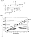
- FIG. 1 is a sectional view of a reactive ion etching (RIE) apparatus which comprises a reaction chamber 2 for subjecting a semiconductor wafer 1 to etching, and a showerhead type upper electrode 3 and a lower electrode 4 arranged, respectively, on upper and lower sides of the reaction chamber 2 in opposed relation to each other.
- RIE reactive ion etching
- RIE apparatus is a parallel plate-type RIE apparatus as depicted in FIG. 1
- active species such as ions and radicals in the plasma are accelerated in a direction toward the semiconductor wafer 1 (direction perpendicular to a wafer surface).
- the active species can etch (anisotropically etch) the semiconductor wafer 1 only in the direction perpendicular to the wafer surface, based on a physical effect and a chemical reaction effect of sputtering, thereby enabling high-accuracy microprocessing.
- an internal space of the reaction chamber 2 is first evacuated to a vacuum state by a vacuum pump (not depicted) connected to an downstream side of an exhaust plate 7, and the etching gas is supplied from the shower head type upper electrode 3.
- the showerhead type upper electrode 3 is composed of a disk-shaped member having a hollow portion 5, and comprising a lower wall formed with a large number of gas supply holes 6 in a showerhead-like arrangement.
- the etching gas is supplied from an etching gas supply source (not depicted) to the hollow portion 5 and then supplied into the reaction chamber 2 through the gas supply holes 6 in a uniform flow rate distribution.
- Patent Document 1 JP 2007-112641 A describes a technique intended to provide a focus ring (edge ring) having plasma resistance to high-density plasma, wherein the focus ring is formed of a sintered composite obtained by: adding an organic binder to an mixed powder of yttria powder and aluminum powder; kneading and forming the resulting mixture to prepare a shaped body; and then burning the shaped body in a hydrogen or inert atmosphere at a temperature of 1520°C or less, wherein the focus ring has a specific resistance (electric resistivity) of less than 10 9 ⁇ • cm.
- Patent Document 2 JP H11-217268A describes a SiC sintered body for a plasma apparatus, which exhibits excellent plasma resistance and has a low risk of particle contamination due to drop-off of particles, wherein the SiC sintered body has a density of 2.7 g/cm 3 or more, an average crystal grain size of 20 ⁇ m or more, a thermal conductivity of 80 W/m • K or more, and an electric resistivity of 10 -2 to 10 2 ⁇ • cm.
- Patent Document 2 discloses sintered bodies using ⁇ -structure silicon carbide (hereinafter referred to as " ⁇ -SiC”) as a primary raw material, in Examples 3 and 5, it also discloses sintered bodies using ⁇ -structure silicon carbide (hereinafter referred to as " ⁇ -SiC”) as a primary raw material in detail in Examples 1, 2 and Comparative Examples 1, 2 with detailed description.
- ⁇ -SiC sintered bodies using ⁇ -SiC as a primary raw material
- properties thereof are not shown, except for the matters described in Table 1.
- Table 1 presents higher values than those of the remaining Examples and Comparative Examples, and, as to electric resistivity, presents relatively high values, specifically, 0.4 ⁇ • cm in Example 3 and 5.0 ⁇ • cm in Example 5.
- the sintered bodies in Examples 3 and 5 are not formed to have particularly excellent properties.
- Example 3 Although the sintered body in Example 3 is sintered at a highest temperature of 2400°C, the density thereof is 3.1 g/cm 3 at most, and the crystal grain size is less than those of Examples 1 and 2. Thus this sintered body is more likely to be charged with electric charges, and is thus inferior in plasma resistance.
- Patent Document 3 JP 2003-095744A includes the following descriptions in paragraph [0008]: "as shown in Sample No.2 to Sample No. 13, the silicon carbide sintered body of the present invention is understand to be a sintering material which is excellent in strength and hardness based on a dense and substantially pore-free microstructure over which a YAG phase is finely dispersed.”(lines 31 to 34 of 5th column); and "When a semiconductor-producing member using the silicon carbide sintered body of the present invention in each of Sample Nos. 2 to 13 and Sample Nos.
- SiC silicon carbide
- the SiC member using ⁇ -SiC as a primary raw material has been considered to cause chamber contamination, because it contains metal impurities such as iron in an amount greater than those in the SiC member prepared by CVD process using ⁇ -SiC as a primary raw material. For this reason, an idea of using ⁇ -SiC as a raw material for a member for a plasma processing apparatus has been unlikely to be created, and plasma resistance of ⁇ -SiC has not been checked in detail.
- Patent Document 4 JP H10-120466A discloses a highly anti-corrosive silicon carbide member usable in a plasma etching apparatus for semiconductor manufacturing, wherein the member is formed of a sintered body with the ⁇ -SiC content of 90% or more by weight.
- Patent Document 5 JP 2001-007082A discloses an electrode plate for plasma etching which is excellent in the plasma resistance and can realize a long durability, wherein the electrode plate is formed of a silicon carbide sintered body mainly comprising ⁇ -SiC of a 6H type.
- Patent Document 4 the member including very small quantities of metal impurities with the iron content of 1 ppm or less, the aluminum content of 5 ppm or less, and the calcium content of 3 ppm or less is used; and it is described that the weight reduction rate is large in ⁇ -SiC which includes 18 ppm of Al as described in Comparative Example 1 (see claim 1, paragraphs 0039 to 0040, and Table 1).
- the raw material SiC powder to be suitably used includes metal elements with total content of 40 ppm or less, preferably 30 ppm or less, more preferably 20 ppm or less, while most preferably 10 ppm or less (paragraph 0027).
- the edge ring described in the Patent Document 1 has a very large specific resistance (electric resistivity) of less than 10 9 ⁇ • cm, and no verification about impurity diffusion has been made. Moreover, it is also not clear whether the plasma resistance of the edge ring in the Patent Document 1 is superior to that of an edge ring formed of SiC.
- an edge ring formed of SiC has excellent properties in terms of plasma resistance, purity and the like, as compared with an edge ring formed of polysilicon, SiO 2 or the like, the edge ring requires a production cost which is about ten times that of the edge ring formed of polysilicon, SiO 2 or the like, because it employs high-purity SiC prepared by a CVD process, or a sintered body obtained by hot-pressing a ⁇ -SiC powder prepared by a CVD process in order to prevent metal contamination in the reaction chamber 2.
- the edge ring formed of SiC is significantly expensive, considering its performance.
- plasma resistance of the SiC prepared by a CVD process or the SiC obtained by hot-pressing a ⁇ -SiC powder prepared by a CVD process is not so high although it has ultra-high purity of 0.1 ppm or less, i.e., an amount of metal impurities is low by one or more digits, and is very costly. Thus, such SiC becomes a factor causing an increase in running cost.
- the member for a plasma etching apparatus formed of the silicon carbide sintered body mainly comprising ⁇ -SiC is used, further increase in the plasma resistance is required.
- the present invention has been made in view of solving the above conventional problem, and an object thereof to provide a SiC member capable of being produced at lower cost with high plasma resistance, and further provide a production method for the SiC member.
- a silicon carbide member for a plasma processing apparatus which consists of a sintered body of an ⁇ -structure silicon carbide containing metal impurities in an amount of more than 20 ppm and 70 ppm or less and an Al impurities in an amount of more than 50 ppm or less, and an oxide-based or non-oxide-based sintering aid (appended claim 1).
- the oxide-based sintering aid comprises Al 2 O 3 and Y 2 O 3 , wherein a total amount of the Al 2 O 3 and the Y 2 O 3 is the range of 3 to 15 weight parts, and an amount of the Y 2 O 3 is one to two times an amount of the Al 2 O 3 (appended claim 2).
- the non-oxide-based sintering aid contains B 4 C in amount of 0.5 to 5 weight parts (appended claim 3).
- the non-oxide-based sintering aid contains boron and carbon, and an amount of boron is 0.4 to 1.6 weight parts, and an amount of carbon is 0.1 to 0.4 weight parts (appended claim 4).
- Al 12 Y 4 O 9 exists in a grain boundary of the ⁇ -structure silicon carbide crystal grain (appended claim 5).
- a method of producing a silicon carbide member for a plasma processing apparatus comprising:
- the ⁇ -structure silicon carbide powder has an average particle size of 0.3 to 3 ⁇ m
- the oxide-based sintering aid comprises Al 2 O 3 and Y 2 O 3 , wherein a total amount of the Al 2 O 3 and the Y 2 O 3 is the range of 3 to 15 weight parts, and an amount of the Y 2 O 3 is one to two times an amount of the Al 2 O 3 (appended claim 7).
- the ⁇ -structure silicon carbide powder has an average particle size of 0.3 to 3 ⁇ m, and the non-oxide-based sintering aid contains B 4 C in amount of 0.5 to 5 weight parts (appended claim 8).
- the fourth step comprises performing the sintering at a temperature of 1800°C to 2200°C and at an inert gas atmosphere pressure of 1 kg/cm 2 to 50 kg/cm 2 , using a high-frequency heating device used in a frequency band of 1000 Hz to 5000 Hz, or at a temperature of 1800°C to 2200°C using an resistance heating argon atmosphere furnace (appended claim 9).
- the Al 2 O 3 has an average particle size of 0.1 to 1 ⁇ m
- the Y 2 O 3 has an average particle size of 1 ⁇ m or less
- the fourth step comprises performing the sintering at a temperature of 1800°C to 2000°C using an argon atmosphere furnace (appended claim 10).
- the silicon carbide member consists of a sintered body of an ⁇ -silicon carbide containing metal impurities such as iron in an amount of more than 20 ppm and 70 ppm or less and an Al impurities in an amount of 50 ppm or less, and an oxide-based or non-oxide-based sintering aid.
- the oxide-based sintering aid comprises Al 2 O 3 and Y 2 O 3 , wherein a total amount of the Al 2 O 3 and the Y 2 O 3 is the range of 3 to 15 weight parts, and an amount of the Y 2 O 3 is one to two times an amount of the Al 2 O 3 .
- the YAM phase component is formed and it becomes possible to further improve the plasma resistance.
- the non-oxide-based sintering aid contains B 4 C in amount of 0.5 to 5 weight parts.
- the non-oxide sintering aid uses boron and carbon in place of B 4 C as the non-oxide sintering aid, so that the non-oxide sintering aid can be readily manufactured by a well-known method.
- Al 12 Y 4 O 9 exists in a grain boundary of the ⁇ -silicon carbide crystal grain.
- the sintering is performed at a temperature of 1800°C to 2200°C and at an inert gas atmosphere pressure of 1 kg/cm 2 to 50 kg/cm 2 , using a high-frequency heating device used in a frequency band of 1000 Hz to 5000 Hz, or at a temperature of 1800°C to 2200°C using an resistance heating argon atmosphere furnace.
- the Al 2 O 3 and the Y 2 O 3 have, respectively, an average particle size of 0.1 to 1 ⁇ m and an average particle size of 1 ⁇ m or less, and the sintering is performed at a temperature of 1800°C to 2000°C using an argon atmosphere furnace.
- ⁇ -SiC particles As a primary raw material, ⁇ -SiC particles (purity: about 98.5%) having an average particle size of 0.6 ⁇ m were employed, wherein the ⁇ -SiC particles was subjected to chemical cleaning to enable impurities therein, such as elements of groups I to VIII of the 4th rows of the periodic table, and oxides, carbides, nitrides, borides or the like of the elements (hereinafter, these are referred to as "4 th row metal impurity”), to becomes minute amount, and enable free SiO 2 components to become 0.3% or less.
- impurities therein such as elements of groups I to VIII of the 4th rows of the periodic table, and oxides, carbides, nitrides, borides or the like of the elements (hereinafter, these are referred to as "4 th row metal impurity"
- impurities of the 4 th row metal impurity as well as the metal impurity such as the Al impurity in the various main raw material samples were analyzed; and as a result, the total amount thereof was 37 to 70 ppm in which the Al impurity was 28 to 45 ppm and the metal impurity other than Al was 9 to 25 ppm.
- a B 4 C raw material powder having a purity of 99% or more and an average particle size of 1 ⁇ m or less was prepared.
- B 4 C as a sintering aid was added to the above ⁇ -SiC raw material powder in respective amounts of 0.5 weight parts, 1.5 weight parts, 2 weight parts, 3 weight parts and 5 weight part to prepare five types of mixed powders, and then 3 weight parts of acrylic-based water-soluble binder as a shaping aid, and pure water as a solvent, were added to respective ones of the mixed powders to prepare three types of mixtures.
- Each of the mixtures was subjected to pulverization using a ball mill pot made of nylon and nylon-coated balls to prepare a slurry, and a granulated powder was prepared from the slurry by using a spray dryer. Further, the granulated powder was subjected to press-forming at a pressing force of 1000 kg/cm 2 to prepare five types of 50 mm-square test pieces.
- test pieces were heated and degreased in a vacuum atmosphere, and after being putting into an argon (Ar) atmosphere furnace, sintered at a temperature of 2160°C to obtain five types of sintered bodies.
- each of the test pieces was formed as a dense sintered body having a density with respect to a theoretical density of 98.1% or more (specific gravity of those blended with 1.5 weight parts of B 4 C was 3.14 or more).
- An edge ring having an outer diameter of about 350 mm, an inner diameter of about 295 mm, and a thickness of about 5 mm can be produced by processing the sintered body having a size appropriate to this dimension.
- a fine Y 2 O 3 powder having a purity of 99.9% or more and an average particle size of 1 ⁇ m or less as another component of the sintering aid for ⁇ -SiC was also preliminarily prepared.
- fine powders of Al 2 O 3 with the purity of 99.99% and of Y 2 O 3 with the purity of 99.9% each having an average particle size of 0.5 ⁇ m or less were preliminarily prepared.
- Example 2 the mixture was subjected to pulverization to prepare a slurry, and a granulated powder was prepared from the slurry by using a spray dryer. Further, the granulated powder was subjected to press-forming at a pressing force of 1000 kg/cm 2 to prepare 50 mm-square test piece.
- test piece was heated and degreased in a vacuum atmosphere, and after being putting into an argon (Ar) atmosphere high-frequency induction heating furnace, sintered at a temperature of 1860°C to obtain the sintered body.
- Ar argon
- test pieces was formed as a dense sintered body having a specific gravity of 3.16 (relative density of 96.3%).
- the shaped body obtained by using the fine powder of Al 2 O 3 with the average particle diameter of 0.5 ⁇ m and Y 2 O 3 with the average particle diameter of 0.5 ⁇ m or less was sintered in a resistance heating Ar atmosphere furnace; as a result, it could be sintered in a comparatively low temperature region of 1800 to 1900°C to obtain the dense sintered body with the specific gravity of 3.18 (relative density of 97%).
- An edge ring having an outer diameter of about 350 mm, an inner diameter of about 295 mm and a thickness of about 5 mm can be produced by processing the sintered body having a size appropriate to this dimension.
- B 4 C as a sintering aid was added to the same ⁇ -SiC raw material powder as that used in Example 1, in an amount of 1.5 weight parts to prepare a mixed powder, and then a methanol solvent was added to the mixed powder without adding any shaping aid to prepare a mixture.
- Example 2 the mixture was subjected to pulverization to prepare a slurry, and the slurry was dried to prepare a shaping powder.
- the shaping powder was sintered by hot pressing under conditions comprising a pressurizing force of 200 kg/cm 2 and a temperature of 2100°C, to obtain a sintered body with the size of 50 mm square.
- test piece was formed as a dense sintered body having a specific gravity of 3.193 (relative density: 99.8%).
- An edge ring having an outer diameter of about 350 mm, an inner diameter of about 295 mm, and a thickness of about 5 mm can be produced by processing a sintered body having a size appropriate to this dimension.
- S1 a commercially available SiC raw material powder with the SiC purity of 98.5%, SiO 2 content of 0.8%, impurity (Fe) of 0.03%, and metal Al of 0.02% was prepared as the raw material for comparison (hereinafter this is referred to as "S2").
- the raw material powder with the purity of 99.9% or more and the average powder particle diameter of 0.5 ⁇ m or less was used.
- Example 2 Similarly to various blended powders were added the acryl-type binder and a solvent (water), and then they were crushed and mixed by means of the nylon-made ball mill pot and nylon-coated balls; and then, the granulated powder thus obtained was press-forming with the applied pressure of 1000 kg/cm 2 to prepare various green bodies with the size of 50 mm square.
- the sintering temperature was controlled in an argon (Ar) atmosphere furnace to prepare the sintered bodies with different specific gravities; and then, the test pieces for assessment of the plasma resistance having the sample size of 20x20 mm square with the thickness of 5 mm were prepared.
- ⁇ -SiC prepared by the CVD method (hereinafter this is referred to as "CVD-SiC"), which is currently widely used as the edge ring member (sample No.: shown as St), the sintered body with a large amount of iron impurities prepared for comparison in Example 4 (sample No.: shown as #1), and the formulated composition of the sintered body prepared in the present Examples (sample No.: shown as #2 to #6), as well as the material characteristics of each, are summarized; and also, the Al 2 O 3 material with the purity of 99.99%, which was filed for patent application as the material for a shower plate (sample No.: shown as #7), was tested for comparison.
- CVD-SiC ⁇ -SiC prepared by the CVD method
- the plasma resistance test was carried out as follows. A small sample piece with the sample area of 20 ⁇ 20 mm and the thickness of 5 mm was plasma-exposed with a microwave-excited plasma apparatus for an 8-inch wafer (manufactured by Tokyo Electron Ltd.), whereby the plasma resistance was assessed with the weight change before and after the etching.
- the plasma conditions were as follows: the source power of 2000 W (frequency of 2.45 GHz), the bias power of 30 W (frequency of 13.56 MHz), the gas flow rate of 60 sccm using SF 6 gas, the pressure of 100 mTorr, and the irradiation time for plasma exposure of 5 hours (total). Because the plasma irradiation for a long time was difficult, the plasma irradiation for a period of 15 minutes was repeated 20 times.
- St in the sample No. column is CVD-SiC, and in #1 and #2, Al 2 O 3 and Y 2 O 3 the sintering adjuvants, are the same while the SiC raw material powders are different, and moreover, the sintered body in #2 has the specific gravity of less than 3.0 by lowering the sintering temperature.
- Fig. 2 is a graph in which the SiC materials shown in Table 1 were subjected to the aforementioned plasma resistance test, and then the mass reduction amount after the plasma irradiation was divided with surface area of the test sample.
- the CVD-SiC which is widely used in the edge ring of the plasma processing apparatus as the material which is excellent among many SiC materials in the particle anti-fouling, in the plasma resistance, etc., shows the largest mass reduction amount.
- the sample No. #2 shows a large mass reduction curve, indicting poor plasma resistance, because the specific gravity of the sintered body is less than 3.0 (relative density of less than 87.3%), namely, because the specific gravity is low.
- the specific gravity thereof is 3.08 (relative density of 96.3%), showing superior plasma resistance to CVD-SiC in spite of a low relative density.
- the SiC raw material with a high iron impurity content of 0.03% (300 ppm) is used; however, the mass reduction amount is half or less of the CVD-SiC, showing excellent plasma resistance.
- #1 includes ion impurities about 100 times as much as those in the silicon carbide member of the present invention, the plasma resistance thereof is inferior to #4 whose relative density is lower than #1. On top of it, there is a metal fouling problem. Therefore, this cannot be a suitable material.
- the specific gravity values of #4, #5, and #6 are 3.13 (relative density of 94.8%), 3.14 (relative density of 95.2%), and 3.15 (relative density of 95.5%), respectively, wherein in all of them not only there is the YAM phase component in the SiC crystal boundary but also the mass reduction amount due to the plasma irradiation tends to be smaller as the relative density becomes higher. Because as compared with the CVD-SiC the mass reduction amounts of #4, #5, and #6 are 35%, 29%, and 25%, respectively, it can be seen that the plasma resistance is increased about 3 to 4 times.
- Al 2 O 3 of #7 which is disclosed in the prior patent as the material for a shower plate shows almost zero as the mass reduction amount caused by the plasma irradiation, so that it is not etched in the level observable in the mass reduction; however, minute amount of Al is sputtered by the ion irradiation from the plasma so as to be scattered into a gas phase thereby adhering to the wafer.
- Al 2 O 3 causes adverse effects such as an increase in the leak current to the device to be manufactured.
- SiC is suitable because the mother material thereof is Si, the same material as the wafer; and C can volatilize more readily than Al with a fluorine gas, so that it does not cause an adverse effect to the device.
- the reason for the high values in the plasma resistance in the sintered bodies of #1, #4, #5, and #6 is presumed as follows. Namely, all of them are dense sintered bodies with the relative densities of about 95% or more; and moreover the YAM phase component (Al 12 Y 4 O 9 ) is present in the crystal grain boundary of SiC thereby intensifying the bonding strength of the crystal grains, and in addition, Al 12 Y 4 O 9 itself has the plasma resistance.
- the plasma resistance of #2 is poor presumably because not only the sintered body thereof is not dense with the specific gravity of 2.87 (relative density of 87%) but also the YAM phase component is not present.
- the impurity concentration of iron (Fe) and nickel (Ni), which is the largest problem in the members such as a shower plate and an edge ring of the plasma processing apparatus, is about 0.01 ppm in CVD-SiC of the sample No. St; and in the ⁇ -SiC raw material powder to be sintered by a hot-press method, it is described that the concentrations of Fe and Ni are 0.05 and 0.05 ppm or less, respectively, so that by using the high purity members it is contemplated not to cause an adverse effect due to the impurities in any member.
- the Si raw material powders comprising ⁇ -SiC used in the sample No. #4, #5, and #6 include 3 to 10 ppm of Fe impurities and 0.5 to 1 ppm of Ni impurities; however, it was confirmed that when the sintering was carried out such that the relative density became 93% or more, content of the impurities in the sintered body was decreased to half or less by measurement with the glow discharge mass spectrometry method.
- Al 2 O 3 has a large heat capacity because of a large specific heat, and moreover, it has a comparatively a low thermal conductivity and a large thermal expansion coefficient; and thus, this is not suitable for rapid heating and cooling in order to increase the operation rate of the plasma apparatus.
- the shower plate When the material obtained by sintering the blended powder of the component comprising the SiC raw material powder and the sintering aid of the present invention so as to give the relative density of 93% or more is applied for the shower plate, not only the dielectric loss thereof is about 10 -1 to 10 -2 , but also the metal impurity content is small; thus, the ratio of the power consumed for self-heating of the shower plate is small, the power being supplied from the high-frequency power supply; and in addition, the flexural strength and thermal conductivity thereof are sufficient, so that this can respond to rapid heating and cooling, and moreover, the plasma resistance is superior to CVD-SiC. Accordingly, the shower plate having a complex shape can be manufactured with a comparatively low cost, and the member for the plasma apparatus sophisticated than ever can be supplied.
- the shower plate 3 in Fig. 1 is electrically insulated from the inner wall, whereby it is used as a plasma-excited electrode by applying a high-frequency power.
- the obtained granulated powder was subjected to press-forming at a pressing force of 1 ton/cm 2 to prepare a shaped body, degreasing the obtained shaped body and then sintering the resulting degreased body in a resistance heating Ar atmosphere furnace at a temperature of 1800 to 1900°C to produce an edge ring having a specific gravity of 3.15 (relative density of 95.5%) and an electric resistivity of 7.6 ⁇ 10 5 ⁇ •cm.
- Crystal structure analysis by X-ray diffraction was carried out to check the material property of this edge ring.
- the X-ray diffraction chart is presented in FIG. 3 .
- This X-ray diffraction chart shows that the peak of the SiC component, and the peak of the YAM phase component (Al 12 Y 4 O 9 ) generated from the sintering aid comprising Al 2 O 3 and Y 2 O 3 , are present.
- the ⁇ -SiC sintered body of the present invention is formed of the material that is formed of Al 12 Y 4 O 9 which is formed by congregation of Al 2 O 3 and Y 2 O 3 that are blended as the sintering aids to the crystal boundary of SiC during the course of sintering.
- the ⁇ -SiC sintered body of the present invention has a microstructure in which Al 2 O 3 and Y 2 O 3 added as a sintering aid are compounded as Al 12 Y 4 O 9 in the SiC crystal grain boundary during sintering process.
- the ⁇ -SiC raw material powder used in the present invention content of the free SiO 2 included in the SiC raw material is reduced to 0.3% or less, so that SiO 2 that is not excellent in the plasma resistance hardly exists in the sintered body material; and moreover, the ⁇ -SiC sintered body without forming much amount of 3Al 2 O 3 ⁇ 2SiO 2 to 2Al 2 O 3 ⁇ SiO 2 or a mullite component such as Al 6 O 13 Si 12 , these being produced by reaction of SiO 2 with Al 2 O 3 that is blended as the sintering aid and having the molecular weights several times as large as SiO 2 , can be formed.
- the free SiO 2 contained in the SiC raw material is reduced to 0.3% or less.
- the ⁇ -SiC raw material powder used in the present invention can produce the ⁇ -SiC sintered body in which mullite component having several times the molecular weight of SiO 2 such as 3Al 2 O 3 ⁇ 2SiO 2 to 2Al 2 O 3 ⁇ SiO 2 or Al 6 O 13 Si 12 is not generated in a large amount even if SiO 2 react with Al 2 O 3 added as a sintering aid.
- Ar/CF 4 was flowed at 20/10 sccm, and a multilayered film of the silicon oxide film and the polysilicon film was etched at a pressure of 1 Pa to form holes.
- electric power of 2000 W at 13.56 MHz was applied to an antenna, and electric power of 1000 W at 13.56 MHz was applied to a substrate on which a silicon wafer was placed.
- This structure can be suitably used to form a vertical gate for a three-dimensional NAND flash memory.
- edge ring produced in present Example is excellent in terms of plasma resistance as compared with the edge ring of the genuine product (CVD-SiC). This reduces the amount of SiC components gasified and released into the gas phase during the etching.
- FIG. 4 is a view depicting a sectional shape of a hole formed in this way, where the left side depicts a sectional shape of the hole formed by using the conventional edge ring, and the right side depicts a sectional shape of the hole formed by using an edge ring formed of the same material characteristics as the sintered bodies prepared by Example 4 of the present invention (#4, #5, and #6).
- the conventional SiC edge ring as the genuine product is etched with F-base radicals, and then the radicals are gasified into SiF 4 , CF 4 or the like and discharged from the edge ring.
- the density and electric potential of the plasma have been different between the center of the wafer and the periphery of the wafer close to the edge ring.
- the rate of gasification of the edge ring by the plasma became smaller as compared with that of the conventional edge ring, so that the distributions of plasma density and electric potential became uniform.
- Such an advantageous effect is not limited to the above process and the etching apparatus used.
- Accuracy of an etching pattern is essential to miniaturization of semiconductors, and exerts a great influence on the yield of semiconductor production.
- the present invention makes it possible to improve the yield of production.
- test piece thereby obtained was sintered at 2180°C in an Ar atmosphere furnace.
- the sintered body with the specific gravity of 3.10 was obtained, so that almost the same results in the material characteristics as those of the material obtained by using B 4 C as the sintering aid could be obtained.
- a mixing amount of B 4 C raw material powder added with respect to total amount of the ⁇ -SiC raw material powder and the B 4 C raw material powder is preferably a range of 0.5 to 5 weight parts, more preferably a range of 1 to 2 weight parts, and the best range of 0.75 to 1.0 weight parts.
- a total mixing amounts of the Al 2 O 3 raw material powder and the Y 2 O 3 raw material powder added to 100 weight parts of the ⁇ -SiC raw material powder were preferably a range of 3 to 15 weight parts, and more preferably a range of 6 to 12 weight parts.
- the mixing ratio of 1 weight part of Al 2 O 3 and 2 weight parts of Y 2 O 3 is convenient.
- the mixing weight of Y 2 O 3 is preferably 1.1 times or more of that of Al 2 O 3 .
Landscapes
- Chemical & Material Sciences (AREA)
- Engineering & Computer Science (AREA)
- Ceramic Engineering (AREA)
- Manufacturing & Machinery (AREA)
- Physics & Mathematics (AREA)
- Materials Engineering (AREA)
- Organic Chemistry (AREA)
- Plasma & Fusion (AREA)
- Analytical Chemistry (AREA)
- Structural Engineering (AREA)
- Inorganic Chemistry (AREA)
- General Chemical & Material Sciences (AREA)
- Chemical Kinetics & Catalysis (AREA)
- Mechanical Engineering (AREA)
- Metallurgy (AREA)
- Thermal Sciences (AREA)
- Ceramic Products (AREA)
- Drying Of Semiconductors (AREA)
Abstract
Description
- Present invention relates to a silicon carbide member for plasma processing apparatus designed to manufacture various semiconductor devices, and a method of producing the silicon carbide member.
- Heretofore, in a manufacturing process of a semiconductor device, plasma processing techniques have been used to perform film-forming and etching for a semiconductor wafer; and in addition, a chamber cleaning using a fluorine-based gas is carried out.
-
FIG. 1 is a sectional view of a reactive ion etching (RIE) apparatus which comprises areaction chamber 2 for subjecting asemiconductor wafer 1 to etching, and a showerhead typeupper electrode 3 and alower electrode 4 arranged, respectively, on upper and lower sides of thereaction chamber 2 in opposed relation to each other. - As a principle, when an etching gas is supplied into the
reaction chamber 2, and electric power is applied from a high-frequency power supply 10 to thelower electrode 4, plasma is generated in thereaction chamber 2. In the case where the RIE apparatus is a parallel plate-type RIE apparatus as depicted inFIG. 1 , upon application of electric power from the high-frequency power supply 10 to thelower electrode 4, a self-bias potential is generated between thesemiconductor wafer 1 and the plasma, and active species such as ions and radicals in the plasma are accelerated in a direction toward the semiconductor wafer 1 (direction perpendicular to a wafer surface). The active species can etch (anisotropically etch) the semiconductor wafer 1 only in the direction perpendicular to the wafer surface, based on a physical effect and a chemical reaction effect of sputtering, thereby enabling high-accuracy microprocessing. - In operation of etching the
semiconductor wafer 1, an internal space of thereaction chamber 2 is first evacuated to a vacuum state by a vacuum pump (not depicted) connected to an downstream side of anexhaust plate 7, and the etching gas is supplied from the shower head typeupper electrode 3. - The showerhead type
upper electrode 3 is composed of a disk-shaped member having ahollow portion 5, and comprising a lower wall formed with a large number ofgas supply holes 6 in a showerhead-like arrangement. The etching gas is supplied from an etching gas supply source (not depicted) to thehollow portion 5 and then supplied into thereaction chamber 2 through thegas supply holes 6 in a uniform flow rate distribution. - After the supply of the etching gas, electric power is applied from the high-
frequency power supply 10 to thelower electrode 4, so that plasma is generated in thereaction chamber 2. Thesemiconductor wafer 1 is etched by active species in the plasma. - Patent Document 1 (
JP 2007-112641 A - Patent Document 2 (
JP H11-217268A Patent Document 2 discloses sintered bodies using α-structure silicon carbide (hereinafter referred to as "α-SiC") as a primary raw material, in Examples 3 and 5, it also discloses sintered bodies using β-structure silicon carbide (hereinafter referred to as "β-SiC") as a primary raw material in detail in Examples 1, 2 and Comparative Examples 1, 2 with detailed description. As regards the sintered bodies using α-SiC as a primary raw material, properties thereof are not shown, except for the matters described in Table 1. Specifically, as to a content rate of free carbon, Table 1 presents higher values than those of the remaining Examples and Comparative Examples, and, as to electric resistivity, presents relatively high values, specifically, 0.4 Ω • cm in Example 3 and 5.0 Ω • cm in Example 5. Thus, the sintered bodies in Examples 3 and 5 are not formed to have particularly excellent properties. - Moreover, although the sintered body in Example 3 is sintered at a highest temperature of 2400°C, the density thereof is 3.1 g/cm3 at most, and the crystal grain size is less than those of Examples 1 and 2. Thus this sintered body is more likely to be charged with electric charges, and is thus inferior in plasma resistance.
- Patent Document 3 (
JP 2003-095744A Patent Document 3 makes no mention of recognition that the sintered body made of the α-phase silicon carbide crystal phase is particularly excellent. - Further, recently, an edge ring formed of silicon carbide (hereinafter referred to as "SiC") having high plasma resistance has become widespread. In this regard, with a view to preventing metal contamination in the
reaction chamber 2, high-purity β-SiC prepared by a chemical vapor deposition (CVD) process, or a sintered body obtained by hot-pressing a SiC powder prepared by a CVD process, is employed, and a primary raw material thereof is β-SiC. - The SiC member using α-SiC as a primary raw material has been considered to cause chamber contamination, because it contains metal impurities such as iron in an amount greater than those in the SiC member prepared by CVD process using β-SiC as a primary raw material. For this reason, an idea of using α-SiC as a raw material for a member for a plasma processing apparatus has been unlikely to be created, and plasma resistance of α-SiC has not been checked in detail.
- Patent Document 4 (
JP H10-120466A - Patent Document 5 (
JP 2001-007082A - However, in
Patent Document 4, the member including very small quantities of metal impurities with the iron content of 1 ppm or less, the aluminum content of 5 ppm or less, and the calcium content of 3 ppm or less is used; and it is described that the weight reduction rate is large in α-SiC which includes 18 ppm of Al as described in Comparative Example 1 (seeclaim 1, paragraphs 0039 to 0040, and Table 1). - In addition, in
Patent Document 5, it is described that the raw material SiC powder to be suitably used includes metal elements with total content of 40 ppm or less, preferably 30 ppm or less, more preferably 20 ppm or less, while most preferably 10 ppm or less (paragraph 0027). -
- Patent Document 1:
JP 2007-112641A - Patent Document 2:
JP H11-217268A - Patent Document 3:
JP 2003-095744A - Patent Document 4:
JP H10-120466A - Patent Document 5:
JP 2001-007082A - The edge ring described in the
Patent Document 1 has a very large specific resistance (electric resistivity) of less than 109 Ω • cm, and no verification about impurity diffusion has been made. Moreover, it is also not clear whether the plasma resistance of the edge ring in thePatent Document 1 is superior to that of an edge ring formed of SiC. - Although an edge ring formed of SiC has excellent properties in terms of plasma resistance, purity and the like, as compared with an edge ring formed of polysilicon, SiO2 or the like, the edge ring requires a production cost which is about ten times that of the edge ring formed of polysilicon, SiO2 or the like, because it employs high-purity SiC prepared by a CVD process, or a sintered body obtained by hot-pressing a β-SiC powder prepared by a CVD process in order to prevent metal contamination in the
reaction chamber 2. Thus, the edge ring formed of SiC is significantly expensive, considering its performance. - Further, plasma resistance of the SiC prepared by a CVD process or the SiC obtained by hot-pressing a β-SiC powder prepared by a CVD process is not so high although it has ultra-high purity of 0.1 ppm or less, i.e., an amount of metal impurities is low by one or more digits, and is very costly. Thus, such SiC becomes a factor causing an increase in running cost. In addition, in the case when the member for a plasma etching apparatus formed of the silicon carbide sintered body mainly comprising α-SiC is used, further increase in the plasma resistance is required.
- The present invention has been made in view of solving the above conventional problem, and an object thereof to provide a SiC member capable of being produced at lower cost with high plasma resistance, and further provide a production method for the SiC member.
- According to a first aspect of the present invention, there is provided a silicon carbide member for a plasma processing apparatus, which consists of a sintered body of an α-structure silicon carbide containing metal impurities in an amount of more than 20 ppm and 70 ppm or less and an Al impurities in an amount of more than 50 ppm or less, and an oxide-based or non-oxide-based sintering aid (appended claim 1).
- Preferably, in a first specific embodiment of the first aspect of the present invention, the oxide-based sintering aid comprises Al2O3 and Y2O3, wherein a total amount of the Al2O3 and the Y2O3 is the range of 3 to 15 weight parts, and an amount of the Y2O3 is one to two times an amount of the Al2O3 (appended claim 2).
- Preferably, in a second specific embodiment of the first aspect of the present invention, the non-oxide-based sintering aid contains B4C in amount of 0.5 to 5 weight parts (appended claim 3).
- In addition, in a third specific embodiment of the first aspect of the present invention, the non-oxide-based sintering aid contains boron and carbon, and an amount of boron is 0.4 to 1.6 weight parts, and an amount of carbon is 0.1 to 0.4 weight parts (appended claim 4).
- Preferably, in a fourth specific embodiment of the first aspect of the present invention, Al12Y4O9 exists in a grain boundary of the α-structure silicon carbide crystal grain (appended claim 5).
- A method of producing a silicon carbide member for a plasma processing apparatus, comprising:
- According to a second aspect of the present invention, there is provided a first step of mixing an α-structure silicon carbide powder and an oxide-based or non-oxide-based sintering aid together, wherein the α-structure silicon carbide powder containing metal impurities in an amount of more than 20 ppm and 70 ppm or less and an Al impurities in an amount of 50 ppm or less;
- a second step of granulating the α-structure silicon carbide powder and the sintering aid mixed together;
- a third step of subjecting a granulated powder obtained in the second step to press forming;
- a fourth step of degreasing a shaped body obtained in the third step and then sintering the resulting degreased body in an inert gas atmosphere furnace; and
- a fifth step of processing a sintered body obtained in the fourth step into a silicon carbide member for a plasma processing apparatus (appended claim 6).
- Preferably, in a first specific embodiment of the second aspect of the present invention, the α-structure silicon carbide powder has an average particle size of 0.3 to 3 µm, and the oxide-based sintering aid comprises Al2O3 and Y2O3, wherein a total amount of the Al2O3 and the Y2O3 is the range of 3 to 15 weight parts, and an amount of the Y2O3 is one to two times an amount of the Al2O3 (appended claim 7).
- Preferably, in a second specific embodiment of the second aspect of the present invention, the α-structure silicon carbide powder has an average particle size of 0.3 to 3 µm, and the non-oxide-based sintering aid contains B4C in amount of 0.5 to 5 weight parts (appended claim 8).
- Preferably, in a third specific embodiment of the second aspect of the present invention, the fourth step comprises performing the sintering at a temperature of 1800°C to 2200°C and at an inert gas atmosphere pressure of 1 kg/cm2 to 50 kg/cm2, using a high-frequency heating device used in a frequency band of 1000 Hz to 5000 Hz, or at a temperature of 1800°C to 2200°C using an resistance heating argon atmosphere furnace (appended claim 9).
- Preferably, in a fourth specific embodiment of the second aspect of the present invention, the Al2O3 has an average particle size of 0.1 to 1 µm, and the Y2O3 has an average particle size of 1 µm or less, wherein the fourth step comprises performing the sintering at a temperature of 1800°C to 2000°C using an argon atmosphere furnace (appended claim 10).
- In the silicon carbide member according to the first aspect of the invention or the method according to the second aspect of the invention, the silicon carbide member consists of a sintered body of an α-silicon carbide containing metal impurities such as iron in an amount of more than 20 ppm and 70 ppm or less and an Al impurities in an amount of 50 ppm or less, and an oxide-based or non-oxide-based sintering aid. Thus, it becomes possible to produce the silicon carbide member with high plasma resistance at low cost without any adverse influence of the metal impurities on a plasma processing apparatus.
- This makes it possible to improve durability of an edge ring or other member for use in various plasma processing apparatuses and realize mass production and cost reduction thereof.
- In the first specific embodiment of the first aspect of the present invention or the first specific embodiment of the second aspect of the present invention, the oxide-based sintering aid comprises Al2O3 and Y2O3, wherein a total amount of the Al2O3 and the Y2O3 is the range of 3 to 15 weight parts, and an amount of the Y2O3 is one to two times an amount of the Al2O3. Thus, in addition to the above advantageous effect, the YAM phase component is formed and it becomes possible to further improve the plasma resistance.
- In the second specific embodiment of the first aspect of the present invention or the second specific embodiment of the second aspect of the present invention, the non-oxide-based sintering aid contains B4C in amount of 0.5 to 5 weight parts. Thus, in addition to the above advantageous effect, there is no problem of the particle adhesion.
- In the third specific embodiment of the first aspect of the present invention uses boron and carbon in place of B4C as the non-oxide sintering aid, so that the non-oxide sintering aid can be readily manufactured by a well-known method.
- In the fourth specific embodiment of the first aspect of the present invention, Al12Y4O9 exists in a grain boundary of the α-silicon carbide crystal grain. Thus, in addition to the above advantageous effect, it becomes possible to provide better plasma resistance in the silicon carbide member.
- In the third specific embodiment of the second aspect of the present invention, the sintering is performed at a temperature of 1800°C to 2200°C and at an inert gas atmosphere pressure of 1 kg/cm2 to 50 kg/cm2, using a high-frequency heating device used in a frequency band of 1000 Hz to 5000 Hz, or at a temperature of 1800°C to 2200°C using an resistance heating argon atmosphere furnace. Thus, in addition to the above advantageous effect, it becomes possible to obtain a more dense sintered body and provide better plasma resistance in the sintered body.
- In the fourth specific embodiment of the second aspect of the present invention, the Al2O3 and the Y2O3 have, respectively, an average particle size of 0.1 to 1 µm and an average particle size of 1 µm or less, and the sintering is performed at a temperature of 1800°C to 2000°C using an argon atmosphere furnace. Thus, in addition to the above advantageous effect, it becomes possible to provide better bonding between grains and provide better plasma resistance in the sintered body.
-
-
FIG. 1 is a sectional view of a reactive ion etching apparatus. -
FIG. 2 is a graph showing the relationship between the plasma irradiation time and the mass reduction amount per unit surface area. -
FIG. 3 is an X-ray diffraction chart of an α-SiC sintered body according to the present invention, wherein the α-SiC sintered body uses Al2O3 and Y2O3 as a sintering aid. - [
Fig. 4 ] This illustrates the cross section shape of the holes formed in a genuine product (CVD-SiC) currently used as the edge ring and the cross section shape of the holes formed in the multilayered film by etching using the edge ring formed of the sintered body of the present invention. -
FIG. 4 is a view depicting a sectional shape of a hole formed in a multilayered film by etching using a conventional edge ring currently commonly used as a genuine product (CVD-SiC) and an inventive edge ring formed of a sintered body according to the present invention. - The present invention will now be described based on various Examples (production process of an edge ring).
- As a primary raw material, α-SiC particles (purity: about 98.5%) having an average particle size of 0.6 µm were employed, wherein the α-SiC particles was subjected to chemical cleaning to enable impurities therein, such as elements of groups I to VIII of the 4th rows of the periodic table, and oxides, carbides, nitrides, borides or the like of the elements (hereinafter, these are referred to as "4th row metal impurity"), to becomes minute amount, and enable free SiO2 components to become 0.3% or less.
- Then, impurities of the 4th row metal impurity as well as the metal impurity such as the Al impurity in the various main raw material samples were analyzed; and as a result, the total amount thereof was 37 to 70 ppm in which the Al impurity was 28 to 45 ppm and the metal impurity other than Al was 9 to 25 ppm.
- Next, as a sintering aid for α-SiC particles, a B4C raw material powder having a purity of 99% or more and an average particle size of 1 µm or less was prepared.
- B4C as a sintering aid was added to the above α-SiC raw material powder in respective amounts of 0.5 weight parts, 1.5 weight parts, 2 weight parts, 3 weight parts and 5 weight part to prepare five types of mixed powders, and then 3 weight parts of acrylic-based water-soluble binder as a shaping aid, and pure water as a solvent, were added to respective ones of the mixed powders to prepare three types of mixtures.
- Each of the mixtures was subjected to pulverization using a ball mill pot made of nylon and nylon-coated balls to prepare a slurry, and a granulated powder was prepared from the slurry by using a spray dryer. Further, the granulated powder was subjected to press-forming at a pressing force of 1000 kg/cm2 to prepare five types of 50 mm-square test pieces.
- The five types of test pieces were heated and degreased in a vacuum atmosphere, and after being putting into an argon (Ar) atmosphere furnace, sintered at a temperature of 2160°C to obtain five types of sintered bodies.
- As a result of measuring the density of each of these sintered bodies, it was proven that each of the test pieces was formed as a dense sintered body having a density with respect to a theoretical density of 98.1% or more (specific gravity of those blended with 1.5 weight parts of B4C was 3.14 or more).
- Meanwhile, the theoretical density of the raw material powder was calculated by using the specific gravity of each component blended, i.e., SiC=3.21, Al2O3=3.987, Y2O3=5.01, and B4C=2.52; and then, the relative density of the sintered body was calculated.
- An edge ring having an outer diameter of about 350 mm, an inner diameter of about 295 mm, and a thickness of about 5 mm can be produced by processing the sintered body having a size appropriate to this dimension.
- The same α-SiC raw material powder as that used in Example 1, and a fine Al2O3 powder having a purity of 99.99% or more and an average particle size of 0.5 µm as one component of the sintering aid for α-SiC were preliminarily prepared.
- A fine Y2O3 powder having a purity of 99.9% or more and an average particle size of 1 µm or less as another component of the sintering aid for α-SiC was also preliminarily prepared.
- Further, fine powders of Al2O3 with the purity of 99.99% and of Y2O3 with the purity of 99.9% each having an average particle size of 0.5 µm or less were preliminarily prepared.
- 3 weight parts of acrylic-based water-soluble binder as a shaping aid and pure water as a solvent were added to the mixture, wherein the mixture consists of 100 weight parts of the α-SiC raw material powder, 2.5 weight parts of the Al2O3 raw material powder and 5 weight parts of the Y2O3 raw material powder.
- As with Example 1, the mixture was subjected to pulverization to prepare a slurry, and a granulated powder was prepared from the slurry by using a spray dryer. Further, the granulated powder was subjected to press-forming at a pressing force of 1000 kg/cm2 to prepare 50 mm-square test piece.
- The test piece was heated and degreased in a vacuum atmosphere, and after being putting into an argon (Ar) atmosphere high-frequency induction heating furnace, sintered at a temperature of 1860°C to obtain the sintered body.
- As a result of density measurement thereof, it was found that the dense sintered body having the specific gravity of 3.16 (relative density of 96.3%) was obtained.
- As a result of measuring the density of the sintered body, it was proven that the test pieces was formed as a dense sintered body having a specific gravity of 3.16 (relative density of 96.3%).
- The shaped body obtained by using the fine powder of Al2O3 with the average particle diameter of 0.5 µm and Y2O3 with the average particle diameter of 0.5 µm or less was sintered in a resistance heating Ar atmosphere furnace; as a result, it could be sintered in a comparatively low temperature region of 1800 to 1900°C to obtain the dense sintered body with the specific gravity of 3.18 (relative density of 97%).
- An edge ring having an outer diameter of about 350 mm, an inner diameter of about 295 mm and a thickness of about 5 mm can be produced by processing the sintered body having a size appropriate to this dimension.
- B4C as a sintering aid was added to the same α-SiC raw material powder as that used in Example 1, in an amount of 1.5 weight parts to prepare a mixed powder, and then a methanol solvent was added to the mixed powder without adding any shaping aid to prepare a mixture.
- As with Example 1, the mixture was subjected to pulverization to prepare a slurry, and the slurry was dried to prepare a shaping powder.
- The shaping powder was sintered by hot pressing under conditions comprising a pressurizing force of 200 kg/cm2 and a temperature of 2100°C, to obtain a sintered body with the size of 50 mm square.
- As a result of measuring the density of the obtained sintered body, it was proven that the test piece was formed as a dense sintered body having a specific gravity of 3.193 (relative density: 99.8%).
- An edge ring having an outer diameter of about 350 mm, an inner diameter of about 295 mm, and a thickness of about 5 mm can be produced by processing a sintered body having a size appropriate to this dimension.
- In order to study the relationship of the blending amount of the SiC raw material powder and the sintering aid with the difference in the density (specific gravity) of the sintered body, and with the plasma resistance, various materials were prepared.
- By using the same raw material powder as the one used in Example 1 (hereinafter this is referred to as "S1"), a commercially available SiC raw material powder with the SiC purity of 98.5%, SiO2 content of 0.8%, impurity (Fe) of 0.03%, and metal Al of 0.02% was prepared as the raw material for comparison (hereinafter this is referred to as "S2").
- With regard to B4C as the sintering aid, the same raw material powder as the one in Example 1 was used.
- With regard to Al2O3 as one component of the oxide sintering aid, the same raw material powder as the one in Example 2 was used.
- With regard to Y2O3 as the other component of the oxide sintering aid, the raw material powder with the purity of 99.9% or more and the average powder particle diameter of 0.5 µm or less was used.
- Similarly to Example 1, to various blended powders were added the acryl-type binder and a solvent (water), and then they were crushed and mixed by means of the nylon-made ball mill pot and nylon-coated balls; and then, the granulated powder thus obtained was press-forming with the applied pressure of 1000 kg/cm2 to prepare various green bodies with the size of 50 mm square.
- After the various green bodies were degreased by heating with a vacuum atmosphere furnace, the sintering temperature was controlled in an argon (Ar) atmosphere furnace to prepare the sintered bodies with different specific gravities; and then, the test pieces for assessment of the plasma resistance having the sample size of 20x20 mm square with the thickness of 5 mm were prepared.
- In Table 1, as the test pieces for the plasma resistance assessment, β-SiC prepared by the CVD method (hereinafter this is referred to as "CVD-SiC"), which is currently widely used as the edge ring member (sample No.: shown as St), the sintered body with a large amount of iron impurities prepared for comparison in Example 4 (sample No.: shown as #1), and the formulated composition of the sintered body prepared in the present Examples (sample No.: shown as #2 to #6), as well as the material characteristics of each, are summarized; and also, the Al2O3 material with the purity of 99.99%, which was filed for patent application as the material for a shower plate (sample No.: shown as #7), was tested for comparison.
[Table 1] Sample No. Formulated Composition Specific Gravity Resistivity (Ω cm) Thermal Conductivity (W/m·K) Hardness (Hv) Flexural Strength (MPa) Dielectric Loss (Note) St CVD-SiC 3.22 1.6 x 10⁶ 245 - - - #1 S2-2%Al2O3-4%Y2O3 3.13 3.7 x 10⁵ 84 1582 389 0.07 #2 S1-2%Al2O3-4%Y2O3 2.87 2.0 x 10⁵ 68 586 230 0.08 #3 S1-1.5%B4C 3.08 1.6 x 10⁸ 146 2326 255 0.52 #4 S1-3.5%Al2O3-7%Y2O3 3.13 1.3 x 10⁶ 99 1539 353 0.11 #5 S1-3.5%Al2O3-7%Y2O3 3.14 - - - 395 - #6 S1-3.5%Al2O3-7%Y2O3, 3.15 1.4 x 10⁷ 92 - 415 - #7 99.99%Al2O3 3.8 - - - 458 10-4 Note: The dielectric loss was measured by applying the power with the frequency of 13.56 MHz. - The plasma resistance test was carried out as follows. A small sample piece with the sample area of 20×20 mm and the thickness of 5 mm was plasma-exposed with a microwave-excited plasma apparatus for an 8-inch wafer (manufactured by Tokyo Electron Ltd.), whereby the plasma resistance was assessed with the weight change before and after the etching. The plasma conditions were as follows: the source power of 2000 W (frequency of 2.45 GHz), the bias power of 30 W (frequency of 13.56 MHz), the gas flow rate of 60 sccm using SF6 gas, the pressure of 100 mTorr, and the irradiation time for plasma exposure of 5 hours (total). Because the plasma irradiation for a long time was difficult, the plasma irradiation for a period of 15 minutes was repeated 20 times.
- Meanwhile, St in the sample No. column is CVD-SiC, and in #1 and #2, Al2O3 and Y2O3 the sintering adjuvants, are the same while the SiC raw material powders are different, and moreover, the sintered body in #2 has the specific gravity of less than 3.0 by lowering the sintering temperature.
- In #4, #5, and #6, reproducibility in production of the sintered body was studied using the same SiC raw material and oxide sintering aids under the same sintering condition, whereby almost the same density of the sintered body was obtained.
-
Fig. 2 is a graph in which the SiC materials shown in Table 1 were subjected to the aforementioned plasma resistance test, and then the mass reduction amount after the plasma irradiation was divided with surface area of the test sample. - In this figure, it can be seen that the CVD-SiC, which is widely used in the edge ring of the plasma processing apparatus as the material which is excellent among many SiC materials in the particle anti-fouling, in the plasma resistance, etc., shows the largest mass reduction amount.
- Next, the
sample No. # 2 shows a large mass reduction curve, indicting poor plasma resistance, because the specific gravity of the sintered body is less than 3.0 (relative density of less than 87.3%), namely, because the specific gravity is low. - In #3 in which the SiC material using the B4C type sintering aid is used, the specific gravity thereof is 3.08 (relative density of 96.3%), showing superior plasma resistance to CVD-SiC in spite of a low relative density.
- In #1, the SiC raw material with a high iron impurity content of 0.03% (300 ppm) is used; however, the mass reduction amount is half or less of the CVD-SiC, showing excellent plasma resistance.
- It is presumed that this is owing to the dense sintered body with the sintered body's specific gravity of 3.13 (relative density of 95.3%), the dielectric loss in the 10-2 level, as well as the presence of the YAM phase component (Al12Y4O9) in the SiC crystal grain boundary.
- However, because #1 includes ion impurities about 100 times as much as those in the silicon carbide member of the present invention, the plasma resistance thereof is inferior to #4 whose relative density is lower than #1. On top of it, there is a metal fouling problem. Therefore, this cannot be a suitable material.
- The specific gravity values of #4, #5, and #6 are 3.13 (relative density of 94.8%), 3.14 (relative density of 95.2%), and 3.15 (relative density of 95.5%), respectively, wherein in all of them not only there is the YAM phase component in the SiC crystal boundary but also the mass reduction amount due to the plasma irradiation tends to be smaller as the relative density becomes higher. Because as compared with the CVD-SiC the mass reduction amounts of #4, #5, and #6 are 35%, 29%, and 25%, respectively, it can be seen that the plasma resistance is increased about 3 to 4 times.
- Meanwhile, because the dielectric loss of #4 is measured in the level of 1×10⁻¹, it is presumed that #5 and #6 show almost the same value as #4.
- Meanwhile, Al2O3 of #7 which is disclosed in the prior patent as the material for a shower plate shows almost zero as the mass reduction amount caused by the plasma irradiation, so that it is not etched in the level observable in the mass reduction; however, minute amount of Al is sputtered by the ion irradiation from the plasma so as to be scattered into a gas phase thereby adhering to the wafer.
- Therefore, Al2O3 causes adverse effects such as an increase in the leak current to the device to be manufactured.
- On the other hand, SiC is suitable because the mother material thereof is Si, the same material as the wafer; and C can volatilize more readily than Al with a fluorine gas, so that it does not cause an adverse effect to the device.
- The reason for the high values in the plasma resistance in the sintered bodies of #1, #4, #5, and #6 is presumed as follows. Namely, all of them are dense sintered bodies with the relative densities of about 95% or more; and moreover the YAM phase component (Al12Y4O9) is present in the crystal grain boundary of SiC thereby intensifying the bonding strength of the crystal grains, and in addition, Al12Y4O9 itself has the plasma resistance.
- For comparison, the plasma resistance of #2 is poor presumably because not only the sintered body thereof is not dense with the specific gravity of 2.87 (relative density of 87%) but also the YAM phase component is not present.
- On the other hand, by using B4C, the non-oxide sintering aid, a dense sintered body with the specific gravity of 3.14 (relative density of 98.2%) was prepared separately from the test sample of #3, and then, the plasma was irradiated to it for the total time of 5 hours under the same condition as Example 4. As a result of the test, it was found that the plasma resistance was significantly increased as compared with #3, because the mass reduction amount of 0.026 mg/mm2, which is about 60% of CVD-SiC, was obtained.
- The impurity concentration of iron (Fe) and nickel (Ni), which is the largest problem in the members such as a shower plate and an edge ring of the plasma processing apparatus, is about 0.01 ppm in CVD-SiC of the sample No. St; and in the β-SiC raw material powder to be sintered by a hot-press method, it is described that the concentrations of Fe and Ni are 0.05 and 0.05 ppm or less, respectively, so that by using the high purity members it is contemplated not to cause an adverse effect due to the impurities in any member.
- On the other hand, the Si raw material powders comprising α-SiC used in the
sample No. # 4, #5, and #6 include 3 to 10 ppm of Fe impurities and 0.5 to 1 ppm of Ni impurities; however, it was confirmed that when the sintering was carried out such that the relative density became 93% or more, content of the impurities in the sintered body was decreased to half or less by measurement with the glow discharge mass spectrometry method. - Especially, it was found that when a high-frequency induction heating method was used as the heating method at the time of manufacturing the sintered body, reduction degree of the iron impurities was large.
- The
sample No. # 3 using B4C as the sintering aid and the sintered body with the relative density of 98.2% showed results somewhat inferior to #4, #5, and #6 in the plasma resistance test; however, because the B4C sintering aid can be volatilized by a fluorine-type gas, the blending amount of the sintering aid can be reduced to 0.5 weight parts, i.e., 1/3 of #3. Therefore, not only the mass reduction amount due to the plasma irradiation can be decreased, but also B and C that are volatilized by the fluorine-type gas do not adhere to the semiconductor wafer as the particle, so that it can be suitably used as the member for the plasma processing apparatus. - Next, in the high purity Al2O3 of the
sample No. # 7, because the mass reduction amount due to the plasma irradiation is almost zero, it appears to be the best as the member for the plasma apparatus; however, minute amount of Al is scattered into a gas phase by sputtering with ion irradiation from the plasma so as to be adhered to the semiconductor wafer thereby causing adverse effects such as an increase in the leak current to the device to be manufactured. - In addition, Al2O3 has a large heat capacity because of a large specific heat, and moreover, it has a comparatively a low thermal conductivity and a large thermal expansion coefficient; and thus, this is not suitable for rapid heating and cooling in order to increase the operation rate of the plasma apparatus.
- When the material obtained by sintering the blended powder of the component comprising the SiC raw material powder and the sintering aid of the present invention so as to give the relative density of 93% or more is applied for the shower plate, not only the dielectric loss thereof is about 10-1 to 10-2, but also the metal impurity content is small; thus, the ratio of the power consumed for self-heating of the shower plate is small, the power being supplied from the high-frequency power supply; and in addition, the flexural strength and thermal conductivity thereof are sufficient, so that this can respond to rapid heating and cooling, and moreover, the plasma resistance is superior to CVD-SiC. Accordingly, the shower plate having a complex shape can be manufactured with a comparatively low cost, and the member for the plasma apparatus sophisticated than ever can be supplied.
- Meanwhile, in this case, the
shower plate 3 inFig. 1 is electrically insulated from the inner wall, whereby it is used as a plasma-excited electrode by applying a high-frequency power. - 100 weight parts of the same α-SiC raw material powder as that used in Example 1, 3.5 weight parts of Al2O3 with the purity of 99.99% and the average particle diameter of 0.5 µm, and 7 weight parts of Y2O3 with the purity of 99.9% and the average particle diameter of 0.5 µm were mixed to prepare a granulated powder. Further, the obtained granulated powder was subjected to press-forming at a pressing force of 1 ton/cm2 to prepare a shaped body, degreasing the obtained shaped body and then sintering the resulting degreased body in a resistance heating Ar atmosphere furnace at a temperature of 1800 to 1900°C to produce an edge ring having a specific gravity of 3.15 (relative density of 95.5%) and an electric resistivity of 7.6 × 10⁵ Ω•cm.
- Crystal structure analysis by X-ray diffraction was carried out to check the material property of this edge ring. The X-ray diffraction chart is presented in
FIG. 3 . - This X-ray diffraction chart shows that the peak of the SiC component, and the peak of the YAM phase component (Al12Y4O9) generated from the sintering aid comprising Al2O3 and Y2O3, are present.
- Meanwhile, as the result of detailed analysis of the crystal structure by the X-ray diffraction, presence of the Y2O3 component was faintly confirmed.
- As a result of detailed crystal structure analysis by X-ray diffraction, it was ascertained that Y2O3 component existed slightly.
- Therefore, it can be said that the α-SiC sintered body of the present invention is formed of the material that is formed of Al12Y4O9 which is formed by congregation of Al2O3 and Y2O3 that are blended as the sintering aids to the crystal boundary of SiC during the course of sintering.
- Therefore, it can be said that the α-SiC sintered body of the present invention has a microstructure in which Al2O3 and Y2O3 added as a sintering aid are compounded as Al12Y4O9 in the SiC crystal grain boundary during sintering process.
- In addition, in the α-SiC raw material powder used in the present invention, content of the free SiO2 included in the SiC raw material is reduced to 0.3% or less, so that SiO2 that is not excellent in the plasma resistance hardly exists in the sintered body material; and moreover, the α-SiC sintered body without forming much amount of 3Al2O3·2SiO2 to 2Al2O3·SiO2 or a mullite component such as Al6O13Si12, these being produced by reaction of SiO2 with Al2O3 that is blended as the sintering aid and having the molecular weights several times as large as SiO2, can be formed.
- In the α-SiC raw material powder used in the present invention, the free SiO2 contained in the SiC raw material is reduced to 0.3% or less. As a result, almost no SiO2, which is not so excellent in plasma resistance, is present in the sintered body material. Furthermore, the α-SiC raw material powder used in the present invention can produce the α-SiC sintered body in which mullite component having several times the molecular weight of SiO2 such as 3Al2O3·2SiO2 to 2Al2O3·SiO2 or Al6O13Si12 is not generated in a large amount even if SiO2 react with Al2O3 added as a sintering aid.
- Next, using a conventional edge ring currently commonly used as a genuine product (CVD-SiC) and an inventive edge ring produced in Example 4, a plasma etching test was conducted under the following conditions.
- In an inductively coupled type plasma etching apparatus for an 8 inch wafer, Ar/CF4 was flowed at 20/10 sccm, and a multilayered film of the silicon oxide film and the polysilicon film was etched at a pressure of 1 Pa to form holes.
- For plasma excitation, electric power of 2000 W at 13.56 MHz was applied to an antenna, and electric power of 1000 W at 13.56 MHz was applied to a substrate on which a silicon wafer was placed.
- This structure can be suitably used to form a vertical gate for a three-dimensional NAND flash memory.
- In addition, the edge ring produced in present Example is excellent in terms of plasma resistance as compared with the edge ring of the genuine product (CVD-SiC). This reduces the amount of SiC components gasified and released into the gas phase during the etching.
-
FIG. 4 is a view depicting a sectional shape of a hole formed in this way, where the left side depicts a sectional shape of the hole formed by using the conventional edge ring, and the right side depicts a sectional shape of the hole formed by using an edge ring formed of the same material characteristics as the sintered bodies prepared by Example 4 of the present invention (#4, #5, and #6). - As can be seen from
FIG. 4 , the conventional SiC edge ring as the genuine product is etched with F-base radicals, and then the radicals are gasified into SiF4, CF4 or the like and discharged from the edge ring. As such, the density and electric potential of the plasma have been different between the center of the wafer and the periphery of the wafer close to the edge ring. - For this reason, abnormality in the etching shape occurred only at the periphery of the wafer, so that control of fine dimensions became difficult, and the yield after etching has been deteriorated.
- On the other hand, in the sintered body according to the present invention, the rate of gasification of the edge ring by the plasma became smaller as compared with that of the conventional edge ring, so that the distributions of plasma density and electric potential became uniform.
- As a result, as shown in
FIG. 4 , it was possible to form vertical holes, and to suppress occurrence of abnormality in the etching shape. This also improved process yield. - Such an advantageous effect is not limited to the above process and the etching apparatus used.
- In recent years, development and improvement of semiconductors has progressed toward increasingly miniaturization, and it is aimed at forming the groove width of plasma etching to 10 nm or less.
- Accuracy of an etching pattern is essential to miniaturization of semiconductors, and exerts a great influence on the yield of semiconductor production. The present invention makes it possible to improve the yield of production.
- After crushing/mixing-granulating-press-forming a mixture of 100 weight parts of the same α-SiC raw material powder as the one used in Example 1, 1.2 weight parts of boron with the purity of 99.99% and the average particle diameter of 1 µm, 0.5 weight parts of carbon back with the average particle diameter of 0.02 µm, and similarly to Example 1, 3.5 weight parts of an acryl-type water-soluble binder and water as the solvent, the test piece thereby obtained was sintered at 2180°C in an Ar atmosphere furnace. As a result, the sintered body with the specific gravity of 3.10 was obtained, so that almost the same results in the material characteristics as those of the material obtained by using B4C as the sintering aid could be obtained.
- Modifications of the Examples will be listed below.
- (1) In Examples 1 to 5, the α-SiC particles having an average particle size of 0.6 µm was employed. However it found that it is possible to obtain a sintered body having equivalent properties as long as the average particle size of the α-SiC is a range of 0.3 to 3 µm, and to obtain a dense sintered body as long as the average particle size of is a range of 0.3 to 1 µm.
- (2) In Examples 1 and 3, the B4C raw material powder having an average particle size of 1 µm or less was employed as a sintering aid, and in Example 2, the fine Al2O3 powder having an average particle size of 0.5 µm and the fine Y2O3 powder having an average particle size of 1 µm or less were employed as a sintering aid.
However, as a result of repeated experiments, it found that it is possible to obtain a sintered body having equivalent properties as long as the average particle size of B4C is a range of 0.3 to 2 µm, and to obtain more dense sintered body as long as the average particle size of B4C is a range of 0.3 to 1 µm.
Further, it is possible to obtain a sintered body having equivalent properties as long as each of the average particle sizes of the fine Al2O3 powder and the fine Y2O3 powder is, respectively, a range of 0.3 to 3 µm, and to obtain a dense sintered body as long as each of the average particle sizes is, respectively, a range of 0.3 to 2 µm. Further, by employing the fine powders having the average particle sizes of 1 µm or less, it is possible to obtain a sintered body having a low temperature sinterability. - (3) In Example 1, the B4C as a sintering aid was added to the α-SiC raw material powder in amount of 0.5 to 5 weight parts. In Example 2, 2.5 weight parts of the Al2O3 raw material powder and 5 weight parts of the Y2O3 raw material powder were each added to 100 weight parts of the α-SiC raw material powder. In Example 3, the B4C as a sintering aid was added to the α-SiC raw material powder in amount of 1.5 weight parts. In Example 4, 2 or 3.5 weight parts of the Al2O3 raw material powder and 4 or 7 weight parts the Y2O3 raw material powder were each added to 100 weight parts of the α-SiC raw material powder. And in Example 5, 3.5 weight parts of the Al2O3 raw material powder and 7 weight parts of the Y2O3 raw material powder were each added to 100 weight parts of the α-SiC raw material powder.
- However, as a result of repeated experiments, when using B4C as a sintering aid, it was found that a mixing amount of B4C raw material powder added with respect to total amount of the α-SiC raw material powder and the B4C raw material powder is preferably a range of 0.5 to 5 weight parts, more preferably a range of 1 to 2 weight parts, and the best range of 0.75 to 1.0 weight parts.
- Further when using the Al2O3 and the Y2O3 as a sintering aid, it was found that a total mixing amounts of the Al2O3 raw material powder and the Y2O3 raw material powder added to 100 weight parts of the α-SiC raw material powder were preferably a range of 3 to 15 weight parts, and more preferably a range of 6 to 12 weight parts.
- Specifically, when the total mixing amount is 3 weight parts, the mixing ratio of 1 weight part of Al2O3 and 2 weight parts of Y2O3 is convenient.
- However, even though the mixing ratio of Al2O3 and Y2O3 was 1: 2 in Example 2, Yam phase component represented by the structural formula of Al12Y4O9 exists in a crystal grain boundary, and an element weight ratio of Al × 12 element to Y × 4 element is 1: 1.098. Therefore, the mixing weight of Y2O3 is preferably 1.1 times or more of that of Al2O3.
- (4) In Example 1, sintering (Argon Sintering) was carried out using B4C as a sintering aid in the argon atmosphere furnace. In Example 2, sintering (High-frequency Sintering) was carried out using Al2O3 and Y2O3 as a sintering aid in the high-frequency induction heating furnace. In Example 3, sintering (Hot Press Sintering) was carried out by the hot press using B4C as a sintering aid. In Example 4, sintering (Argon Sintering) was carried out using Al2O3 and Y2O3 as a sintering aid. However, high-frequency sintering may be performed using B4C as a sintering aid, or hot press sintering may be performed using Al2O3 and Y2O3 as sintering aids.
- (5) As to the sintering process, the SiC member sintered in an inert atmosphere furnace is further subjected to HIP processing, and thereby it is possible to obtain a dense sintered body having very few holes.
For example, a SiC member was obtained by adding 1.5 weight parts of B4C and sintering in an inert atmosphere furnace to have a specific gravity of 3.144 (relative density of 97.9%), and this obtained SiC member was further subjected to HIP processing at 2000 atmospheric pressure and 2000°C for 1.5 hours. As a result, the resulting SiC member could be densified to have the specific gravity of 3.185 (relative density 99.3%).
Although Ar is used as the atmospheric gas during high-temperature sintering of the SiC member of the present invention, an inert gas other than Ar, or non-oxidizing atmosphere gas can also be used. - (6) In Examples 1 and 2, with regard to the impurities included in the α-SiC raw material powder, an amount of the metal impurity was 37 to 70 ppm, an amount of the Al impurity was 28 to 45 ppm, and an amount of the metal impurity other than Al was 9 to 25 ppm. As a result of the tests on various raw material powders, with regard to the impurities included in the α-SiC raw material powder, it was found that with regard to the metal impurity other than Al it is better when an amount thereof is smaller and that with regard to the Al impurity it is good even when an amount thereof is somewhat large. Therefore, it can be said that it is good when a total amount is more than 20 ppm and 70 ppm or less, an amount of the Al impurity is 50 ppm or less, and an amount of the metal impurity other than Al is 20 ppm or less.
More preferably, a total amount is more than 20 ppm and 60 ppm or less, an amount of the Al impurity is 45 ppm or less, and an amount of the metal impurity other than Al is 15 ppm or less, while still more preferably a total amount is 55 ppm or less, an amount of the Al impurity is 45 ppm or less, and an amount of the metal impurity other than Al is 10 ppm or less. - (7) From Examples 1 to 5, various characteristics required for the member for the plasma processing apparatus can be satisfied when the relative density of the sintered body is 93.0% or more, more preferably 93.9% or more, and the dielectric loss is less than 1×10⁻¹, and the YAM phase component is present in the SiC crystal grain boundary of the sintered body, in some cases the YAP phase component (AlYO3) or the YAG phase (Al15Y3O12) is slightly present, and the average crystal particle diameter of the SiC crystal is 10 µm or less, preferably 7 µm or less, while more preferably 5 µm or less.
-
- 1
- Semiconductor wafer
- 2
- Reaction chamber
- 3
- Shower head type upper electrode
- 4
- Lower electrode
- 5
- Hollow portion
- 6
- Gas supply hole
- 7
- Exhaust plate
- 8
- Electrostatic chuck
- 9
- Edge ring
- 10
- High-frequency power supply
Claims (10)
- A silicon carbide member for a plasma processing apparatus, which consists of a sintered body of an α-structure silicon carbide containing metal impurities in an amount of more than 20 ppm and 70 ppm or less and an Al impurities in an amount of 50 ppm or less, and an oxide-based or non-oxide-based sintering aid.
- The silicon carbide member as recited in claim 1, wherein the oxide-based sintering aid comprises Al2O3 and Y2O3, wherein a total amount of the Al2O3 and the Y2O3 is the range of 3 to 15 weight parts, and an amount of the Y2O3 is one to two times an amount of the Al2O3.
- The silicon carbide member as recited in claim 1, wherein the non-oxide-based sintering aid contains B4C in amount of 0.5 to 5 weight parts.
- The silicon carbide member as recited in claim 1, wherein the non-oxide-based sintering aid contains boron and carbon, and amount of boron is 0.4 to 1.6 weight parts, and amount of carbon is 0.1 to 0.4 weight parts.
- The silicon carbide member as recited in claim 1 or 2, wherein Al12Y4O9 exists in a grain boundary of the α-structure silicon carbide crystal grain.
- A method of producing a silicon carbide member for a plasma processing apparatus, comprising:a first step of mixing an α-structure silicon carbide powder and an oxide-based or non-oxide-based sintering aid together, wherein the α-structure silicon carbide powder containing metal impurities in an amount of more than 20 ppm and 70 ppm or less and an Al impurities in an amount of 50 ppm or less;a second step of granulating the α-structure silicon carbide powder and the sintering aid mixed together;a third step of subjecting a granulated powder obtained in the second step to press forming;a fourth step of degreasing a shaped body obtained in the third step and then sintering the resulting degreased body in an inert gas atmosphere furnace; anda fifth step of processing a sintered body obtained in the fourth step into a silicon carbide member for a plasma processing apparatus.
- The method as recited in claim 6, wherein the α-structure silicon carbide powder has an average particle size of 0.3 to 3 µm, and the oxide-based sintering aid comprises Al2O3 and Y2O3, wherein a total amount of the Al2O3 and the Y2O3 is the range of 3 to 15 weight parts, and an amount of the Y2O3 is one to two times an amount of the Al2O3.
- The method as recited in claim 6, wherein the α-structure silicon carbide powder has an average particle size of 0.3 to 3 µm, and the non-oxide-based sintering aid contains B4C in amount of 0.5 to 5 weight parts.
- The method as recited in any one of claims 6 to 8, wherein the fourth step comprises performing the sintering at a temperature of 1800°C to 2200°C and at an inert gas atmosphere pressure of 1 kg/cm2 to 50 kg/cm2, using a high-frequency heating device used in a frequency band of 1000 Hz to 5000 Hz, or at a temperature of 1800°C to 2200°C using an resistance heating argon atmosphere furnace.
- The method as recited in claim 7, wherein the Al2O3 has an average particle size of 0.1 to 1 µm, and the Y2O3 has an average particle size of 1 µm or less, wherein the fourth step comprises performing the sintering at a temperature of 1800°C to 2000°C using an argon atmosphere furnace.
Applications Claiming Priority (2)
| Application Number | Priority Date | Filing Date | Title |
|---|---|---|---|
| JP2016188361 | 2016-09-27 | ||
| PCT/JP2017/033102 WO2018061778A1 (en) | 2016-09-27 | 2017-09-13 | Silicon carbide member for plasma treatment apparatus, and method of manufacturing same |
Publications (3)
| Publication Number | Publication Date |
|---|---|
| EP3521264A1 true EP3521264A1 (en) | 2019-08-07 |
| EP3521264A4 EP3521264A4 (en) | 2020-05-27 |
| EP3521264B1 EP3521264B1 (en) | 2024-07-24 |
Family
ID=61762850
Family Applications (1)
| Application Number | Title | Priority Date | Filing Date |
|---|---|---|---|
| EP17855734.4A Active EP3521264B1 (en) | 2016-09-27 | 2017-09-13 | Silicon carbide member for plasma processing apparatus |
Country Status (5)
| Country | Link |
|---|---|
| US (1) | US11264214B2 (en) |
| EP (1) | EP3521264B1 (en) |
| JP (1) | JP6960636B2 (en) |
| TW (1) | TWI737801B (en) |
| WO (1) | WO2018061778A1 (en) |
Families Citing this family (7)
| Publication number | Priority date | Publication date | Assignee | Title |
|---|---|---|---|---|
| US20200051793A1 (en) | 2018-08-13 | 2020-02-13 | Skc Solmics Co., Ltd. | Ring-shaped element for etcher and method for etching substrate using the same |
| JP7412923B2 (en) * | 2019-08-23 | 2024-01-15 | 東京エレクトロン株式会社 | Edge ring, plasma treatment equipment, and edge ring manufacturing method |
| JP7454983B2 (en) * | 2020-03-30 | 2024-03-25 | 東京エレクトロン株式会社 | Edge ring and plasma treatment equipment |
| JPWO2022080277A1 (en) * | 2020-10-16 | 2022-04-21 | ||
| CN117693607A (en) * | 2021-07-30 | 2024-03-12 | Agc株式会社 | Components for semiconductor manufacturing equipment and methods of manufacturing such components |
| WO2023008439A1 (en) * | 2021-07-30 | 2023-02-02 | Agc株式会社 | Member for semiconductor production apparatus and method for producing said member |
| CN119054041A (en) * | 2022-03-23 | 2024-11-29 | 朗姆研究公司 | Spark plasma sintering assembly for low temperature plasma processing chamber |
Family Cites Families (18)
| Publication number | Priority date | Publication date | Assignee | Title |
|---|---|---|---|---|
| TW341558B (en) * | 1995-05-18 | 1998-10-01 | Ind Tech Res Inst | Method of fabricating self-reinforced pressureless sintered silicon carbide |
| EP0771769A3 (en) * | 1995-11-06 | 1997-07-23 | Dow Corning | Sintering alpha silicon carbide powder with multiple sintering aids |
| DE69722873T2 (en) | 1996-08-27 | 2004-05-19 | Asahi Glass Co., Ltd. | High corrosion resistant silicon carbide product |
| JPH10120466A (en) * | 1996-08-27 | 1998-05-12 | Asahi Glass Co Ltd | High corrosion resistance silicon carbide member and use thereof |
| DE19746008A1 (en) * | 1997-10-20 | 1999-04-22 | Bayer Ag | Sintering additive- and silica-containing silicon nitride material has high acid resistance |
| JPH11217268A (en) | 1998-01-28 | 1999-08-10 | Ibiden Co Ltd | Silicon carbide sintered compact for plasma apparatus and its production |
| JP2001007082A (en) * | 1999-06-18 | 2001-01-12 | Asahi Glass Co Ltd | Electrode plate for plasma etching |
| DE10146393A1 (en) * | 2001-09-20 | 2003-04-17 | Wacker Chemie Gmbh | Non-magnetic sintered body based on SiC and its use |
| JP2003095744A (en) | 2001-09-21 | 2003-04-03 | Nippon Tungsten Co Ltd | Silicon carbide sintered body, semiconductor manufacturing member using the same, magnetic head manufacturing member, wear-resistant sliding member, and method of manufacturing the same |
| JP2003176178A (en) * | 2001-12-07 | 2003-06-24 | Nhk Spring Co Ltd | Wafer support and its peripheral parts |
| JP2005267931A (en) * | 2004-03-17 | 2005-09-29 | Sumitomo Electric Ind Ltd | Heater unit |
| JP2007112641A (en) | 2005-10-18 | 2007-05-10 | Toshiba Ceramics Co Ltd | Focus ring |
| NO335994B1 (en) * | 2011-10-13 | 2015-04-13 | Saint Gobain Ceramic Mat As | Process for producing grains useful for the preparation of a silicon carbide-based sintered product, composite grains prepared by the process, and use of the grains. |
| US11091370B2 (en) * | 2013-05-02 | 2021-08-17 | Pallidus, Inc. | Polysilocarb based silicon carbide materials, applications and devices |
| CN103641482A (en) * | 2013-10-25 | 2014-03-19 | 宁夏机械研究院(有限责任公司) | Preparation method for self-lubricating silicon carbide ceramic sealing material |
| RU2707772C2 (en) * | 2014-09-25 | 2019-11-29 | Мелиор Инновейшнз, Инк. | Polysilocarb based silicon carbide materials, applications and devices |
| US10280121B2 (en) * | 2015-03-31 | 2019-05-07 | Hokuriku Seikei Industrial Co., Ltd. | Silicon carbide member for plasma processing apparatus |
| WO2017018599A1 (en) * | 2015-07-29 | 2017-02-02 | 한국기계연구원 | Silicon carbide powder, silicon carbide sintered body, silicon carbide slurry, and preparation method therefor |
-
2017
- 2017-09-13 JP JP2018542365A patent/JP6960636B2/en active Active
- 2017-09-13 EP EP17855734.4A patent/EP3521264B1/en active Active
- 2017-09-13 WO PCT/JP2017/033102 patent/WO2018061778A1/en not_active Ceased
- 2017-09-13 US US16/307,534 patent/US11264214B2/en not_active Expired - Fee Related
- 2017-09-15 TW TW106129893A patent/TWI737801B/en not_active IP Right Cessation
Also Published As
| Publication number | Publication date |
|---|---|
| JPWO2018061778A1 (en) | 2019-09-12 |
| JP6960636B2 (en) | 2021-11-05 |
| WO2018061778A1 (en) | 2018-04-05 |
| TW201833061A (en) | 2018-09-16 |
| TWI737801B (en) | 2021-09-01 |
| US11264214B2 (en) | 2022-03-01 |
| EP3521264A4 (en) | 2020-05-27 |
| EP3521264B1 (en) | 2024-07-24 |
| US20190304755A1 (en) | 2019-10-03 |
Similar Documents
| Publication | Publication Date | Title |
|---|---|---|
| EP3521264B1 (en) | Silicon carbide member for plasma processing apparatus | |
| EP3279923B1 (en) | Silicon carbide member for plasma treatment devices, and method for manufacturing same | |
| US11014853B2 (en) | Y2O3—ZrO2 erosion resistant material for chamber components in plasma environments | |
| US9837296B2 (en) | Electrostatic chuck apparatus | |
| EP1245696A2 (en) | Plasma resistant member | |
| KR101457215B1 (en) | Yttrium oxide material, member for semiconductor manufacturing apparatus and method for manufacturing yttrium oxide material | |
| US7989380B2 (en) | High resistivity SiC material with B, N and O as the only additions | |
| EP1972599B1 (en) | Yttrium oxide-containing material, component of semiconductor manufacturing equipment, and method of producing yttrium oxide-containing material | |
| CN116134003A (en) | Large size sintered yttrium oxide body | |
| JP2006069843A (en) | Ceramic member for semiconductor manufacturing apparatus | |
| JP2020170804A (en) | A member for a plasma processing device and a plasma processing device including the member. | |
| KR102744847B1 (en) | Sintered body and parts comprising the same | |
| KR102771534B1 (en) | Sintered body and parts comprising the same | |
| WO2010024353A1 (en) | Corrosion-resistant member and method for manufacture thereof | |
| US20240290583A1 (en) | Electrostatic chuck, electrostatic chuck heater comprising same, and semiconductor holding device | |
| WO2023008439A1 (en) | Member for semiconductor production apparatus and method for producing said member | |
| KR102833575B1 (en) | YAG sintered body comprising excess Al, member for plasma etching device including the same, and manufacturing method thereof | |
| CN100396647C (en) | Yttrium oxide sintered body and manufacturing method thereof | |
| US20040154543A1 (en) | Wafer holder for semiconductor manufacturing device and semiconductor manufacturing device in which it is installed | |
| WO2025136943A1 (en) | Beryllium aluminate based dielectric material for semiconductor manufacturing and processing applications | |
| JP2002003277A (en) | Manufacturing method of aluminum nitride sintered body | |
| JP2006240960A (en) | High resistivity silicon carbide sintered body | |
| US20040182322A1 (en) | Wafer holder for semiconductor manufacturing device and semiconductor manufacturing device in which it is installed | |
| JP2009149496A (en) | Electroconductive ceramic material |
Legal Events
| Date | Code | Title | Description |
|---|---|---|---|
| STAA | Information on the status of an ep patent application or granted ep patent |
Free format text: STATUS: THE INTERNATIONAL PUBLICATION HAS BEEN MADE |
|
| PUAI | Public reference made under article 153(3) epc to a published international application that has entered the european phase |
Free format text: ORIGINAL CODE: 0009012 |
|
| STAA | Information on the status of an ep patent application or granted ep patent |
Free format text: STATUS: REQUEST FOR EXAMINATION WAS MADE |
|
| 17P | Request for examination filed |
Effective date: 20181205 |
|
| AK | Designated contracting states |
Kind code of ref document: A1 Designated state(s): AL AT BE BG CH CY CZ DE DK EE ES FI FR GB GR HR HU IE IS IT LI LT LU LV MC MK MT NL NO PL PT RO RS SE SI SK SM TR |
|
| AX | Request for extension of the european patent |
Extension state: BA ME |
|
| DAV | Request for validation of the european patent (deleted) | ||
| DAX | Request for extension of the european patent (deleted) | ||
| REG | Reference to a national code |
Ref country code: DE Ref legal event code: R079 Free format text: PREVIOUS MAIN CLASS: C04B0035569000 Ipc: C04B0035565000 Ref document number: 602017083578 Country of ref document: DE |
|
| A4 | Supplementary search report drawn up and despatched |
Effective date: 20200423 |
|
| RIC1 | Information provided on ipc code assigned before grant |
Ipc: C04B 35/575 20060101ALI20200417BHEP Ipc: C04B 35/626 20060101ALI20200417BHEP Ipc: C04B 35/565 20060101AFI20200417BHEP Ipc: H01L 21/3065 20060101ALI20200417BHEP Ipc: H01J 37/32 20060101ALI20200417BHEP Ipc: C04B 35/645 20060101ALI20200417BHEP |
|
| GRAP | Despatch of communication of intention to grant a patent |
Free format text: ORIGINAL CODE: EPIDOSNIGR1 |
|
| STAA | Information on the status of an ep patent application or granted ep patent |
Free format text: STATUS: GRANT OF PATENT IS INTENDED |
|
| INTG | Intention to grant announced |
Effective date: 20231031 |
|
| GRAJ | Information related to disapproval of communication of intention to grant by the applicant or resumption of examination proceedings by the epo deleted |
Free format text: ORIGINAL CODE: EPIDOSDIGR1 |
|
| STAA | Information on the status of an ep patent application or granted ep patent |
Free format text: STATUS: REQUEST FOR EXAMINATION WAS MADE |
|
| GRAP | Despatch of communication of intention to grant a patent |
Free format text: ORIGINAL CODE: EPIDOSNIGR1 |
|
| STAA | Information on the status of an ep patent application or granted ep patent |
Free format text: STATUS: GRANT OF PATENT IS INTENDED |
|
| INTC | Intention to grant announced (deleted) | ||
| INTG | Intention to grant announced |
Effective date: 20240405 |
|
| GRAS | Grant fee paid |
Free format text: ORIGINAL CODE: EPIDOSNIGR3 |
|
| GRAA | (expected) grant |
Free format text: ORIGINAL CODE: 0009210 |
|
| STAA | Information on the status of an ep patent application or granted ep patent |
Free format text: STATUS: THE PATENT HAS BEEN GRANTED |
|
| AK | Designated contracting states |
Kind code of ref document: B1 Designated state(s): AL AT BE BG CH CY CZ DE DK EE ES FI FR GB GR HR HU IE IS IT LI LT LU LV MC MK MT NL NO PL PT RO RS SE SI SK SM TR |
|
| P01 | Opt-out of the competence of the unified patent court (upc) registered |
Free format text: CASE NUMBER: APP_36407/2024 Effective date: 20240618 |
|
| REG | Reference to a national code |
Ref country code: GB Ref legal event code: FG4D |
|
| REG | Reference to a national code |
Ref country code: CH Ref legal event code: EP |
|
| REG | Reference to a national code |
Ref country code: IE Ref legal event code: FG4D Ref country code: DE Ref legal event code: R096 Ref document number: 602017083578 Country of ref document: DE |
|
| REG | Reference to a national code |
Ref country code: NL Ref legal event code: FP |
|
| PGFP | Annual fee paid to national office [announced via postgrant information from national office to epo] |
Ref country code: FR Payment date: 20240909 Year of fee payment: 8 |
|
| PGFP | Annual fee paid to national office [announced via postgrant information from national office to epo] |
Ref country code: NL Payment date: 20240911 Year of fee payment: 8 |
|
| REG | Reference to a national code |
Ref country code: LT Ref legal event code: MG9D |
|
| PG25 | Lapsed in a contracting state [announced via postgrant information from national office to epo] |
Ref country code: PT Free format text: LAPSE BECAUSE OF FAILURE TO SUBMIT A TRANSLATION OF THE DESCRIPTION OR TO PAY THE FEE WITHIN THE PRESCRIBED TIME-LIMIT Effective date: 20241125 |
|
| REG | Reference to a national code |
Ref country code: AT Ref legal event code: MK05 Ref document number: 1706194 Country of ref document: AT Kind code of ref document: T Effective date: 20240724 |
|
| PG25 | Lapsed in a contracting state [announced via postgrant information from national office to epo] |
Ref country code: PT Free format text: LAPSE BECAUSE OF FAILURE TO SUBMIT A TRANSLATION OF THE DESCRIPTION OR TO PAY THE FEE WITHIN THE PRESCRIBED TIME-LIMIT Effective date: 20241125 |
|
| PGFP | Annual fee paid to national office [announced via postgrant information from national office to epo] |
Ref country code: DE Payment date: 20240930 Year of fee payment: 8 |
|
| PG25 | Lapsed in a contracting state [announced via postgrant information from national office to epo] |
Ref country code: NO Free format text: LAPSE BECAUSE OF FAILURE TO SUBMIT A TRANSLATION OF THE DESCRIPTION OR TO PAY THE FEE WITHIN THE PRESCRIBED TIME-LIMIT Effective date: 20241024 |
|
| PG25 | Lapsed in a contracting state [announced via postgrant information from national office to epo] |
Ref country code: FI Free format text: LAPSE BECAUSE OF FAILURE TO SUBMIT A TRANSLATION OF THE DESCRIPTION OR TO PAY THE FEE WITHIN THE PRESCRIBED TIME-LIMIT Effective date: 20240724 Ref country code: GR Free format text: LAPSE BECAUSE OF FAILURE TO SUBMIT A TRANSLATION OF THE DESCRIPTION OR TO PAY THE FEE WITHIN THE PRESCRIBED TIME-LIMIT Effective date: 20241025 Ref country code: PL Free format text: LAPSE BECAUSE OF FAILURE TO SUBMIT A TRANSLATION OF THE DESCRIPTION OR TO PAY THE FEE WITHIN THE PRESCRIBED TIME-LIMIT Effective date: 20240724 |
|
| PG25 | Lapsed in a contracting state [announced via postgrant information from national office to epo] |
Ref country code: BG Free format text: LAPSE BECAUSE OF FAILURE TO SUBMIT A TRANSLATION OF THE DESCRIPTION OR TO PAY THE FEE WITHIN THE PRESCRIBED TIME-LIMIT Effective date: 20240724 |
|
| PG25 | Lapsed in a contracting state [announced via postgrant information from national office to epo] |
Ref country code: LV Free format text: LAPSE BECAUSE OF FAILURE TO SUBMIT A TRANSLATION OF THE DESCRIPTION OR TO PAY THE FEE WITHIN THE PRESCRIBED TIME-LIMIT Effective date: 20240724 |
|
| PG25 | Lapsed in a contracting state [announced via postgrant information from national office to epo] |
Ref country code: IS Free format text: LAPSE BECAUSE OF FAILURE TO SUBMIT A TRANSLATION OF THE DESCRIPTION OR TO PAY THE FEE WITHIN THE PRESCRIBED TIME-LIMIT Effective date: 20241124 Ref country code: AT Free format text: LAPSE BECAUSE OF FAILURE TO SUBMIT A TRANSLATION OF THE DESCRIPTION OR TO PAY THE FEE WITHIN THE PRESCRIBED TIME-LIMIT Effective date: 20240724 |
|
| PG25 | Lapsed in a contracting state [announced via postgrant information from national office to epo] |
Ref country code: HR Free format text: LAPSE BECAUSE OF FAILURE TO SUBMIT A TRANSLATION OF THE DESCRIPTION OR TO PAY THE FEE WITHIN THE PRESCRIBED TIME-LIMIT Effective date: 20240724 |
|
| PG25 | Lapsed in a contracting state [announced via postgrant information from national office to epo] |
Ref country code: RS Free format text: LAPSE BECAUSE OF FAILURE TO SUBMIT A TRANSLATION OF THE DESCRIPTION OR TO PAY THE FEE WITHIN THE PRESCRIBED TIME-LIMIT Effective date: 20241024 Ref country code: ES Free format text: LAPSE BECAUSE OF FAILURE TO SUBMIT A TRANSLATION OF THE DESCRIPTION OR TO PAY THE FEE WITHIN THE PRESCRIBED TIME-LIMIT Effective date: 20240724 |
|
| PG25 | Lapsed in a contracting state [announced via postgrant information from national office to epo] |
Ref country code: RS Free format text: LAPSE BECAUSE OF FAILURE TO SUBMIT A TRANSLATION OF THE DESCRIPTION OR TO PAY THE FEE WITHIN THE PRESCRIBED TIME-LIMIT Effective date: 20241024 Ref country code: PL Free format text: LAPSE BECAUSE OF FAILURE TO SUBMIT A TRANSLATION OF THE DESCRIPTION OR TO PAY THE FEE WITHIN THE PRESCRIBED TIME-LIMIT Effective date: 20240724 Ref country code: NO Free format text: LAPSE BECAUSE OF FAILURE TO SUBMIT A TRANSLATION OF THE DESCRIPTION OR TO PAY THE FEE WITHIN THE PRESCRIBED TIME-LIMIT Effective date: 20241024 Ref country code: LV Free format text: LAPSE BECAUSE OF FAILURE TO SUBMIT A TRANSLATION OF THE DESCRIPTION OR TO PAY THE FEE WITHIN THE PRESCRIBED TIME-LIMIT Effective date: 20240724 Ref country code: IS Free format text: LAPSE BECAUSE OF FAILURE TO SUBMIT A TRANSLATION OF THE DESCRIPTION OR TO PAY THE FEE WITHIN THE PRESCRIBED TIME-LIMIT Effective date: 20241124 Ref country code: HR Free format text: LAPSE BECAUSE OF FAILURE TO SUBMIT A TRANSLATION OF THE DESCRIPTION OR TO PAY THE FEE WITHIN THE PRESCRIBED TIME-LIMIT Effective date: 20240724 Ref country code: GR Free format text: LAPSE BECAUSE OF FAILURE TO SUBMIT A TRANSLATION OF THE DESCRIPTION OR TO PAY THE FEE WITHIN THE PRESCRIBED TIME-LIMIT Effective date: 20241025 Ref country code: FI Free format text: LAPSE BECAUSE OF FAILURE TO SUBMIT A TRANSLATION OF THE DESCRIPTION OR TO PAY THE FEE WITHIN THE PRESCRIBED TIME-LIMIT Effective date: 20240724 Ref country code: ES Free format text: LAPSE BECAUSE OF FAILURE TO SUBMIT A TRANSLATION OF THE DESCRIPTION OR TO PAY THE FEE WITHIN THE PRESCRIBED TIME-LIMIT Effective date: 20240724 Ref country code: BG Free format text: LAPSE BECAUSE OF FAILURE TO SUBMIT A TRANSLATION OF THE DESCRIPTION OR TO PAY THE FEE WITHIN THE PRESCRIBED TIME-LIMIT Effective date: 20240724 Ref country code: AT Free format text: LAPSE BECAUSE OF FAILURE TO SUBMIT A TRANSLATION OF THE DESCRIPTION OR TO PAY THE FEE WITHIN THE PRESCRIBED TIME-LIMIT Effective date: 20240724 |
|
| PG25 | Lapsed in a contracting state [announced via postgrant information from national office to epo] |
Ref country code: RO Free format text: LAPSE BECAUSE OF FAILURE TO SUBMIT A TRANSLATION OF THE DESCRIPTION OR TO PAY THE FEE WITHIN THE PRESCRIBED TIME-LIMIT Effective date: 20240724 Ref country code: SM Free format text: LAPSE BECAUSE OF FAILURE TO SUBMIT A TRANSLATION OF THE DESCRIPTION OR TO PAY THE FEE WITHIN THE PRESCRIBED TIME-LIMIT Effective date: 20240724 Ref country code: DK Free format text: LAPSE BECAUSE OF FAILURE TO SUBMIT A TRANSLATION OF THE DESCRIPTION OR TO PAY THE FEE WITHIN THE PRESCRIBED TIME-LIMIT Effective date: 20240724 |
|
| PG25 | Lapsed in a contracting state [announced via postgrant information from national office to epo] |
Ref country code: MC Free format text: LAPSE BECAUSE OF FAILURE TO SUBMIT A TRANSLATION OF THE DESCRIPTION OR TO PAY THE FEE WITHIN THE PRESCRIBED TIME-LIMIT Effective date: 20240724 Ref country code: EE Free format text: LAPSE BECAUSE OF FAILURE TO SUBMIT A TRANSLATION OF THE DESCRIPTION OR TO PAY THE FEE WITHIN THE PRESCRIBED TIME-LIMIT Effective date: 20240724 |
|
| PG25 | Lapsed in a contracting state [announced via postgrant information from national office to epo] |
Ref country code: CZ Free format text: LAPSE BECAUSE OF FAILURE TO SUBMIT A TRANSLATION OF THE DESCRIPTION OR TO PAY THE FEE WITHIN THE PRESCRIBED TIME-LIMIT Effective date: 20240724 |
|
| REG | Reference to a national code |
Ref country code: DE Ref legal event code: R097 Ref document number: 602017083578 Country of ref document: DE |
|
| PG25 | Lapsed in a contracting state [announced via postgrant information from national office to epo] |
Ref country code: SK Free format text: LAPSE BECAUSE OF FAILURE TO SUBMIT A TRANSLATION OF THE DESCRIPTION OR TO PAY THE FEE WITHIN THE PRESCRIBED TIME-LIMIT Effective date: 20240724 Ref country code: IT Free format text: LAPSE BECAUSE OF FAILURE TO SUBMIT A TRANSLATION OF THE DESCRIPTION OR TO PAY THE FEE WITHIN THE PRESCRIBED TIME-LIMIT Effective date: 20240724 |
|
| REG | Reference to a national code |
Ref country code: CH Ref legal event code: PL |
|
| PG25 | Lapsed in a contracting state [announced via postgrant information from national office to epo] |
Ref country code: LU Free format text: LAPSE BECAUSE OF NON-PAYMENT OF DUE FEES Effective date: 20240913 |
|
| PLBE | No opposition filed within time limit |
Free format text: ORIGINAL CODE: 0009261 |
|
| STAA | Information on the status of an ep patent application or granted ep patent |
Free format text: STATUS: NO OPPOSITION FILED WITHIN TIME LIMIT |
|
| GBPC | Gb: european patent ceased through non-payment of renewal fee |
Effective date: 20241024 |
|
| 26N | No opposition filed |
Effective date: 20250425 |
|
| PG25 | Lapsed in a contracting state [announced via postgrant information from national office to epo] |
Ref country code: GB Free format text: LAPSE BECAUSE OF NON-PAYMENT OF DUE FEES Effective date: 20241024 |
|
| REG | Reference to a national code |
Ref country code: BE Ref legal event code: MM Effective date: 20240930 |
|
| PG25 | Lapsed in a contracting state [announced via postgrant information from national office to epo] |
Ref country code: BE Free format text: LAPSE BECAUSE OF NON-PAYMENT OF DUE FEES Effective date: 20240930 |
|
| PG25 | Lapsed in a contracting state [announced via postgrant information from national office to epo] |
Ref country code: CH Free format text: LAPSE BECAUSE OF NON-PAYMENT OF DUE FEES Effective date: 20240930 |
|
| PG25 | Lapsed in a contracting state [announced via postgrant information from national office to epo] |
Ref country code: IE Free format text: LAPSE BECAUSE OF NON-PAYMENT OF DUE FEES Effective date: 20240913 |
|
| PG25 | Lapsed in a contracting state [announced via postgrant information from national office to epo] |
Ref country code: SE Free format text: LAPSE BECAUSE OF FAILURE TO SUBMIT A TRANSLATION OF THE DESCRIPTION OR TO PAY THE FEE WITHIN THE PRESCRIBED TIME-LIMIT Effective date: 20240724 |
|
| PG25 | Lapsed in a contracting state [announced via postgrant information from national office to epo] |
Ref country code: CY Free format text: LAPSE BECAUSE OF FAILURE TO SUBMIT A TRANSLATION OF THE DESCRIPTION OR TO PAY THE FEE WITHIN THE PRESCRIBED TIME-LIMIT; INVALID AB INITIO Effective date: 20170913 |
|
| PG25 | Lapsed in a contracting state [announced via postgrant information from national office to epo] |
Ref country code: HU Free format text: LAPSE BECAUSE OF FAILURE TO SUBMIT A TRANSLATION OF THE DESCRIPTION OR TO PAY THE FEE WITHIN THE PRESCRIBED TIME-LIMIT; INVALID AB INITIO Effective date: 20170913 |
|
| REG | Reference to a national code |
Ref country code: DE Ref legal event code: R119 Ref document number: 602017083578 Country of ref document: DE |
|
| REG | Reference to a national code |
Ref country code: NL Ref legal event code: MM Effective date: 20251001 |
|
| PG25 | Lapsed in a contracting state [announced via postgrant information from national office to epo] |
Ref country code: TR Free format text: LAPSE BECAUSE OF FAILURE TO SUBMIT A TRANSLATION OF THE DESCRIPTION OR TO PAY THE FEE WITHIN THE PRESCRIBED TIME-LIMIT Effective date: 20240724 |
|
| PG25 | Lapsed in a contracting state [announced via postgrant information from national office to epo] |
Ref country code: SI Free format text: LAPSE BECAUSE OF FAILURE TO SUBMIT A TRANSLATION OF THE DESCRIPTION OR TO PAY THE FEE WITHIN THE PRESCRIBED TIME-LIMIT Effective date: 20240724 |
|
| PG25 | Lapsed in a contracting state [announced via postgrant information from national office to epo] |
Ref country code: NL Free format text: LAPSE BECAUSE OF NON-PAYMENT OF DUE FEES Effective date: 20251001 |
|
| PG25 | Lapsed in a contracting state [announced via postgrant information from national office to epo] |
Ref country code: LT Free format text: LAPSE BECAUSE OF FAILURE TO SUBMIT A TRANSLATION OF THE DESCRIPTION OR TO PAY THE FEE WITHIN THE PRESCRIBED TIME-LIMIT Effective date: 20240724 |
|
| PG25 | Lapsed in a contracting state [announced via postgrant information from national office to epo] |
Ref country code: DE Free format text: LAPSE BECAUSE OF NON-PAYMENT OF DUE FEES Effective date: 20260401 |
|
| PG25 | Lapsed in a contracting state [announced via postgrant information from national office to epo] |
Ref country code: FR Free format text: LAPSE BECAUSE OF NON-PAYMENT OF DUE FEES Effective date: 20250930 |