EP3520906A1 - Production method for film - Google Patents
Production method for film Download PDFInfo
- Publication number
- EP3520906A1 EP3520906A1 EP17855649.4A EP17855649A EP3520906A1 EP 3520906 A1 EP3520906 A1 EP 3520906A1 EP 17855649 A EP17855649 A EP 17855649A EP 3520906 A1 EP3520906 A1 EP 3520906A1
- Authority
- EP
- European Patent Office
- Prior art keywords
- film
- substrate
- raw material
- material solution
- coating blade
- Prior art date
- Legal status (The legal status is an assumption and is not a legal conclusion. Google has not performed a legal analysis and makes no representation as to the accuracy of the status listed.)
- Withdrawn
Links
- 238000004519 manufacturing process Methods 0.000 title description 18
- 238000000576 coating method Methods 0.000 claims abstract description 187
- 239000011248 coating agent Substances 0.000 claims abstract description 182
- 239000000758 substrate Substances 0.000 claims abstract description 171
- 239000002994 raw material Substances 0.000 claims abstract description 146
- 238000000034 method Methods 0.000 claims abstract description 90
- 239000000463 material Substances 0.000 claims abstract description 38
- 239000002904 solvent Substances 0.000 claims abstract description 38
- 238000001035 drying Methods 0.000 claims abstract description 9
- 239000004065 semiconductor Substances 0.000 claims description 69
- 239000013078 crystal Substances 0.000 claims description 29
- 238000009751 slip forming Methods 0.000 claims description 7
- 238000009835 boiling Methods 0.000 claims description 3
- 239000010408 film Substances 0.000 abstract description 245
- 239000010409 thin film Substances 0.000 abstract description 37
- 239000007788 liquid Substances 0.000 description 40
- 230000015572 biosynthetic process Effects 0.000 description 24
- 239000011521 glass Substances 0.000 description 22
- 230000037230 mobility Effects 0.000 description 19
- 239000010410 layer Substances 0.000 description 18
- 230000000052 comparative effect Effects 0.000 description 14
- 238000001704 evaporation Methods 0.000 description 11
- 230000008020 evaporation Effects 0.000 description 11
- -1 polyethylene terephthalate Polymers 0.000 description 6
- RDOXTESZEPMUJZ-UHFFFAOYSA-N anisole Chemical compound COC1=CC=CC=C1 RDOXTESZEPMUJZ-UHFFFAOYSA-N 0.000 description 4
- 238000004090 dissolution Methods 0.000 description 4
- ZWEHNKRNPOVVGH-UHFFFAOYSA-N 2-Butanone Chemical compound CCC(C)=O ZWEHNKRNPOVVGH-UHFFFAOYSA-N 0.000 description 3
- CSCPPACGZOOCGX-UHFFFAOYSA-N Acetone Chemical compound CC(C)=O CSCPPACGZOOCGX-UHFFFAOYSA-N 0.000 description 3
- UHOVQNZJYSORNB-UHFFFAOYSA-N Benzene Chemical compound C1=CC=CC=C1 UHOVQNZJYSORNB-UHFFFAOYSA-N 0.000 description 3
- RTZKZFJDLAIYFH-UHFFFAOYSA-N Diethyl ether Chemical compound CCOCC RTZKZFJDLAIYFH-UHFFFAOYSA-N 0.000 description 3
- OKKJLVBELUTLKV-UHFFFAOYSA-N Methanol Chemical compound OC OKKJLVBELUTLKV-UHFFFAOYSA-N 0.000 description 3
- ZMXDDKWLCZADIW-UHFFFAOYSA-N N,N-Dimethylformamide Chemical compound CN(C)C=O ZMXDDKWLCZADIW-UHFFFAOYSA-N 0.000 description 3
- 238000000151 deposition Methods 0.000 description 3
- 230000008021 deposition Effects 0.000 description 3
- 230000003028 elevating effect Effects 0.000 description 3
- 238000010438 heat treatment Methods 0.000 description 3
- 230000003287 optical effect Effects 0.000 description 3
- 239000004033 plastic Substances 0.000 description 3
- 229920003023 plastic Polymers 0.000 description 3
- 238000004804 winding Methods 0.000 description 3
- AEOCOSISEQLPHY-UHFFFAOYSA-N 2,8-difluoro-5,11-bis(triethylsilylethynyl)anthradithiophene Chemical compound C1=C2C(C#C[Si](CC)(CC)CC)=C(C=C3C(SC(F)=C3)=C3)C3=C(C#C[Si](CC)(CC)CC)C2=CC2=C1SC(F)=C2 AEOCOSISEQLPHY-UHFFFAOYSA-N 0.000 description 2
- 229920002284 Cellulose triacetate Polymers 0.000 description 2
- 229920000089 Cyclic olefin copolymer Polymers 0.000 description 2
- IAZDPXIOMUYVGZ-UHFFFAOYSA-N Dimethylsulphoxide Chemical compound CS(C)=O IAZDPXIOMUYVGZ-UHFFFAOYSA-N 0.000 description 2
- LFQSCWFLJHTTHZ-UHFFFAOYSA-N Ethanol Chemical compound CCO LFQSCWFLJHTTHZ-UHFFFAOYSA-N 0.000 description 2
- 239000004698 Polyethylene Substances 0.000 description 2
- 239000004642 Polyimide Substances 0.000 description 2
- 239000004743 Polypropylene Substances 0.000 description 2
- KAESVJOAVNADME-UHFFFAOYSA-N Pyrrole Chemical compound C=1C=CNC=1 KAESVJOAVNADME-UHFFFAOYSA-N 0.000 description 2
- WYURNTSHIVDZCO-UHFFFAOYSA-N Tetrahydrofuran Chemical compound C1CCOC1 WYURNTSHIVDZCO-UHFFFAOYSA-N 0.000 description 2
- YTPLMLYBLZKORZ-UHFFFAOYSA-N Thiophene Chemical compound C=1C=CSC=1 YTPLMLYBLZKORZ-UHFFFAOYSA-N 0.000 description 2
- NNLVGZFZQQXQNW-ADJNRHBOSA-N [(2r,3r,4s,5r,6s)-4,5-diacetyloxy-3-[(2s,3r,4s,5r,6r)-3,4,5-triacetyloxy-6-(acetyloxymethyl)oxan-2-yl]oxy-6-[(2r,3r,4s,5r,6s)-4,5,6-triacetyloxy-2-(acetyloxymethyl)oxan-3-yl]oxyoxan-2-yl]methyl acetate Chemical compound O([C@@H]1O[C@@H]([C@H]([C@H](OC(C)=O)[C@H]1OC(C)=O)O[C@H]1[C@@H]([C@@H](OC(C)=O)[C@H](OC(C)=O)[C@@H](COC(C)=O)O1)OC(C)=O)COC(=O)C)[C@@H]1[C@@H](COC(C)=O)O[C@@H](OC(C)=O)[C@H](OC(C)=O)[C@H]1OC(C)=O NNLVGZFZQQXQNW-ADJNRHBOSA-N 0.000 description 2
- RWBMMASKJODNSV-UHFFFAOYSA-N [1]benzothiolo[2,3-g][1]benzothiole Chemical class C1=CC=C2C3=C(SC=C4)C4=CC=C3SC2=C1 RWBMMASKJODNSV-UHFFFAOYSA-N 0.000 description 2
- MCEWYIDBDVPMES-UHFFFAOYSA-N [60]pcbm Chemical compound C123C(C4=C5C6=C7C8=C9C%10=C%11C%12=C%13C%14=C%15C%16=C%17C%18=C(C=%19C=%20C%18=C%18C%16=C%13C%13=C%11C9=C9C7=C(C=%20C9=C%13%18)C(C7=%19)=C96)C6=C%11C%17=C%15C%13=C%15C%14=C%12C%12=C%10C%10=C85)=C9C7=C6C2=C%11C%13=C2C%15=C%12C%10=C4C23C1(CCCC(=O)OC)C1=CC=CC=C1 MCEWYIDBDVPMES-UHFFFAOYSA-N 0.000 description 2
- 239000003849 aromatic solvent Substances 0.000 description 2
- 238000006243 chemical reaction Methods 0.000 description 2
- 239000011651 chromium Substances 0.000 description 2
- 150000001875 compounds Chemical class 0.000 description 2
- 239000000470 constituent Substances 0.000 description 2
- 230000003247 decreasing effect Effects 0.000 description 2
- 230000000994 depressogenic effect Effects 0.000 description 2
- 239000010931 gold Substances 0.000 description 2
- RBTKNAXYKSUFRK-UHFFFAOYSA-N heliogen blue Chemical compound [Cu].[N-]1C2=C(C=CC=C3)C3=C1N=C([N-]1)C3=CC=CC=C3C1=NC([N-]1)=C(C=CC=C3)C3=C1N=C([N-]1)C3=CC=CC=C3C1=N2 RBTKNAXYKSUFRK-UHFFFAOYSA-N 0.000 description 2
- RAXXELZNTBOGNW-UHFFFAOYSA-N imidazole Natural products C1=CNC=N1 RAXXELZNTBOGNW-UHFFFAOYSA-N 0.000 description 2
- 229910052751 metal Inorganic materials 0.000 description 2
- 239000002184 metal Substances 0.000 description 2
- UZKWTJUDCOPSNM-UHFFFAOYSA-N methoxybenzene Substances CCCCOC=C UZKWTJUDCOPSNM-UHFFFAOYSA-N 0.000 description 2
- 230000006911 nucleation Effects 0.000 description 2
- 238000010899 nucleation Methods 0.000 description 2
- 229920000301 poly(3-hexylthiophene-2,5-diyl) polymer Polymers 0.000 description 2
- 229920000573 polyethylene Polymers 0.000 description 2
- 229920000139 polyethylene terephthalate Polymers 0.000 description 2
- 239000005020 polyethylene terephthalate Substances 0.000 description 2
- 229920001721 polyimide Polymers 0.000 description 2
- 229920001155 polypropylene Polymers 0.000 description 2
- 238000004381 surface treatment Methods 0.000 description 2
- FMZQNTNMBORAJM-UHFFFAOYSA-N tri(propan-2-yl)-[2-[13-[2-tri(propan-2-yl)silylethynyl]pentacen-6-yl]ethynyl]silane Chemical compound C1=CC=C2C=C3C(C#C[Si](C(C)C)(C(C)C)C(C)C)=C(C=C4C(C=CC=C4)=C4)C4=C(C#C[Si](C(C)C)(C(C)C)C(C)C)C3=CC2=C1 FMZQNTNMBORAJM-UHFFFAOYSA-N 0.000 description 2
- 238000001771 vacuum deposition Methods 0.000 description 2
- 239000012855 volatile organic compound Substances 0.000 description 2
- HXEYQGSFZZKULR-UHFFFAOYSA-N 1,2,3,4-tetramethylpentacene Chemical compound C1=CC=CC2=CC3=CC4=CC5=C(C)C(C)=C(C)C(C)=C5C=C4C=C3C=C21 HXEYQGSFZZKULR-UHFFFAOYSA-N 0.000 description 1
- SBJIDUSVEICMRY-UHFFFAOYSA-N 2,7-diphenyl-[1]benzothiolo[3,2-b][1]benzothiole Chemical compound C1=CC=CC=C1C1=CC=C2C(SC3=CC(=CC=C33)C=4C=CC=CC=4)=C3SC2=C1 SBJIDUSVEICMRY-UHFFFAOYSA-N 0.000 description 1
- GTAQUECFRVEPNA-UHFFFAOYSA-N 9,23-didecyl-14,28-dithiaheptacyclo[15.11.0.03,15.04,13.06,11.018,27.020,25]octacosa-1(17),2,4(13),5,7,9,11,15,18(27),19,21,23,25-tridecaene Chemical compound S1C2=CC3=CC(CCCCCCCCCC)=CC=C3C=C2C2=C1C=C1C3=CC4=CC=C(CCCCCCCCCC)C=C4C=C3SC1=C2 GTAQUECFRVEPNA-UHFFFAOYSA-N 0.000 description 1
- 239000004925 Acrylic resin Substances 0.000 description 1
- 229920000178 Acrylic resin Polymers 0.000 description 1
- LSNNMFCWUKXFEE-UHFFFAOYSA-M Bisulfite Chemical compound OS([O-])=O LSNNMFCWUKXFEE-UHFFFAOYSA-M 0.000 description 1
- WKBOTKDWSSQWDR-UHFFFAOYSA-N Bromine atom Chemical compound [Br] WKBOTKDWSSQWDR-UHFFFAOYSA-N 0.000 description 1
- XMWRBQBLMFGWIX-UHFFFAOYSA-N C60 fullerene Chemical class C12=C3C(C4=C56)=C7C8=C5C5=C9C%10=C6C6=C4C1=C1C4=C6C6=C%10C%10=C9C9=C%11C5=C8C5=C8C7=C3C3=C7C2=C1C1=C2C4=C6C4=C%10C6=C9C9=C%11C5=C5C8=C3C3=C7C1=C1C2=C4C6=C2C9=C5C3=C12 XMWRBQBLMFGWIX-UHFFFAOYSA-N 0.000 description 1
- ZAMOUSCENKQFHK-UHFFFAOYSA-N Chlorine atom Chemical compound [Cl] ZAMOUSCENKQFHK-UHFFFAOYSA-N 0.000 description 1
- VYZAMTAEIAYCRO-UHFFFAOYSA-N Chromium Chemical compound [Cr] VYZAMTAEIAYCRO-UHFFFAOYSA-N 0.000 description 1
- NTIZESTWPVYFNL-UHFFFAOYSA-N Methyl isobutyl ketone Chemical compound CC(C)CC(C)=O NTIZESTWPVYFNL-UHFFFAOYSA-N 0.000 description 1
- UIHCLUNTQKBZGK-UHFFFAOYSA-N Methyl isobutyl ketone Natural products CCC(C)C(C)=O UIHCLUNTQKBZGK-UHFFFAOYSA-N 0.000 description 1
- FXHOOIRPVKKKFG-UHFFFAOYSA-N N,N-Dimethylacetamide Chemical compound CN(C)C(C)=O FXHOOIRPVKKKFG-UHFFFAOYSA-N 0.000 description 1
- 239000004952 Polyamide Substances 0.000 description 1
- 239000004793 Polystyrene Substances 0.000 description 1
- VYPSYNLAJGMNEJ-UHFFFAOYSA-N Silicium dioxide Chemical compound O=[Si]=O VYPSYNLAJGMNEJ-UHFFFAOYSA-N 0.000 description 1
- BQCADISMDOOEFD-UHFFFAOYSA-N Silver Chemical compound [Ag] BQCADISMDOOEFD-UHFFFAOYSA-N 0.000 description 1
- NXCSDJOTXUWERI-UHFFFAOYSA-N [1]benzothiolo[3,2-b][1]benzothiole Chemical compound C12=CC=CC=C2SC2=C1SC1=CC=CC=C21 NXCSDJOTXUWERI-UHFFFAOYSA-N 0.000 description 1
- 239000012790 adhesive layer Substances 0.000 description 1
- 239000005456 alcohol based solvent Substances 0.000 description 1
- 150000001408 amides Chemical class 0.000 description 1
- 230000003321 amplification Effects 0.000 description 1
- 125000003118 aryl group Chemical group 0.000 description 1
- 229920001400 block copolymer Polymers 0.000 description 1
- GDTBXPJZTBHREO-UHFFFAOYSA-N bromine Substances BrBr GDTBXPJZTBHREO-UHFFFAOYSA-N 0.000 description 1
- 229910052794 bromium Inorganic materials 0.000 description 1
- 229910052799 carbon Inorganic materials 0.000 description 1
- 239000003153 chemical reaction reagent Substances 0.000 description 1
- 229910052801 chlorine Inorganic materials 0.000 description 1
- 239000000460 chlorine Substances 0.000 description 1
- 229910052804 chromium Inorganic materials 0.000 description 1
- 229920001577 copolymer Polymers 0.000 description 1
- RBSLJAJQOVYTRQ-UHFFFAOYSA-N croconic acid Chemical compound OC1=C(O)C(=O)C(=O)C1=O RBSLJAJQOVYTRQ-UHFFFAOYSA-N 0.000 description 1
- 238000002109 crystal growth method Methods 0.000 description 1
- 238000002425 crystallisation Methods 0.000 description 1
- 230000008025 crystallization Effects 0.000 description 1
- 230000007423 decrease Effects 0.000 description 1
- CZWHMRTTWFJMBC-UHFFFAOYSA-N dinaphtho[2,3-b:2',3'-f]thieno[3,2-b]thiophene Chemical compound C1=CC=C2C=C(SC=3C4=CC5=CC=CC=C5C=C4SC=33)C3=CC2=C1 CZWHMRTTWFJMBC-UHFFFAOYSA-N 0.000 description 1
- AMDQVKPUZIXQFC-UHFFFAOYSA-N dinaphthylene dioxide Chemical compound O1C(C2=C34)=CC=CC2=CC=C3OC2=CC=CC3=CC=C1C4=C32 AMDQVKPUZIXQFC-UHFFFAOYSA-N 0.000 description 1
- 230000005611 electricity Effects 0.000 description 1
- 238000005516 engineering process Methods 0.000 description 1
- 239000004210 ether based solvent Substances 0.000 description 1
- 239000005038 ethylene vinyl acetate Substances 0.000 description 1
- 238000011156 evaluation Methods 0.000 description 1
- 229910003472 fullerene Inorganic materials 0.000 description 1
- PCHJSUWPFVWCPO-UHFFFAOYSA-N gold Chemical compound [Au] PCHJSUWPFVWCPO-UHFFFAOYSA-N 0.000 description 1
- 229910052737 gold Inorganic materials 0.000 description 1
- 230000005484 gravity Effects 0.000 description 1
- 229910052736 halogen Inorganic materials 0.000 description 1
- 150000002367 halogens Chemical class 0.000 description 1
- 239000005453 ketone based solvent Substances 0.000 description 1
- 238000012423 maintenance Methods 0.000 description 1
- 238000005259 measurement Methods 0.000 description 1
- 238000012986 modification Methods 0.000 description 1
- 230000004048 modification Effects 0.000 description 1
- 239000002105 nanoparticle Substances 0.000 description 1
- 238000003199 nucleic acid amplification method Methods 0.000 description 1
- 150000002964 pentacenes Chemical class 0.000 description 1
- AZVQGIPHTOBHAF-UHFFFAOYSA-N perfluoropentacene Chemical compound FC1=C(F)C(F)=C(F)C2=C(F)C3=C(F)C4=C(F)C5=C(F)C(F)=C(F)C(F)=C5C(F)=C4C(F)=C3C(F)=C21 AZVQGIPHTOBHAF-UHFFFAOYSA-N 0.000 description 1
- 238000009832 plasma treatment Methods 0.000 description 1
- 229920002647 polyamide Polymers 0.000 description 1
- 229920000515 polycarbonate Polymers 0.000 description 1
- 239000004417 polycarbonate Substances 0.000 description 1
- 229920000728 polyester Polymers 0.000 description 1
- 239000011112 polyethylene naphthalate Substances 0.000 description 1
- 229920000098 polyolefin Polymers 0.000 description 1
- 229920002223 polystyrene Polymers 0.000 description 1
- 229920000123 polythiophene Polymers 0.000 description 1
- 230000003252 repetitive effect Effects 0.000 description 1
- 229920005989 resin Polymers 0.000 description 1
- 239000011347 resin Substances 0.000 description 1
- 238000000926 separation method Methods 0.000 description 1
- 229910052710 silicon Inorganic materials 0.000 description 1
- 239000010703 silicon Substances 0.000 description 1
- 229910052709 silver Inorganic materials 0.000 description 1
- 239000004332 silver Substances 0.000 description 1
- 238000004528 spin coating Methods 0.000 description 1
- 229910001220 stainless steel Inorganic materials 0.000 description 1
- 239000010935 stainless steel Substances 0.000 description 1
- 239000000126 substance Substances 0.000 description 1
- HXJUTPCZVOIRIF-UHFFFAOYSA-N sulfolane Chemical compound O=S1(=O)CCCC1 HXJUTPCZVOIRIF-UHFFFAOYSA-N 0.000 description 1
- NYBWUHOMYZZKOR-UHFFFAOYSA-N tes-adt Chemical compound C1=C2C(C#C[Si](CC)(CC)CC)=C(C=C3C(SC=C3)=C3)C3=C(C#C[Si](CC)(CC)CC)C2=CC2=C1SC=C2 NYBWUHOMYZZKOR-UHFFFAOYSA-N 0.000 description 1
- YLQBMQCUIZJEEH-UHFFFAOYSA-N tetrahydrofuran Natural products C=1C=COC=1 YLQBMQCUIZJEEH-UHFFFAOYSA-N 0.000 description 1
- NMFKEMBATXKZSP-UHFFFAOYSA-N thieno[3,2-b]thiophene Chemical compound S1C=CC2=C1C=CS2.S1C=CC2=C1C=CS2 NMFKEMBATXKZSP-UHFFFAOYSA-N 0.000 description 1
- HNDGEYCCZGRMTN-UHFFFAOYSA-N thieno[3,2-f:4,5-f]bis[1]benzothiophene Chemical compound S1C2=CC=3SC=CC=3C=C2C2=C1C=C(SC=C1)C1=C2 HNDGEYCCZGRMTN-UHFFFAOYSA-N 0.000 description 1
- 229930192474 thiophene Natural products 0.000 description 1
- 125000000391 vinyl group Chemical group [H]C([*])=C([H])[H] 0.000 description 1
- 229920002554 vinyl polymer Polymers 0.000 description 1
Images





Classifications
-
- H—ELECTRICITY
- H10—SEMICONDUCTOR DEVICES; ELECTRIC SOLID-STATE DEVICES NOT OTHERWISE PROVIDED FOR
- H10K—ORGANIC ELECTRIC SOLID-STATE DEVICES
- H10K71/00—Manufacture or treatment specially adapted for the organic devices covered by this subclass
- H10K71/10—Deposition of organic active material
- H10K71/12—Deposition of organic active material using liquid deposition, e.g. spin coating
- H10K71/15—Deposition of organic active material using liquid deposition, e.g. spin coating characterised by the solvent used
-
- B—PERFORMING OPERATIONS; TRANSPORTING
- B05—SPRAYING OR ATOMISING IN GENERAL; APPLYING FLUENT MATERIALS TO SURFACES, IN GENERAL
- B05D—PROCESSES FOR APPLYING FLUENT MATERIALS TO SURFACES, IN GENERAL
- B05D1/00—Processes for applying liquids or other fluent materials
- B05D1/26—Processes for applying liquids or other fluent materials performed by applying the liquid or other fluent material from an outlet device in contact with, or almost in contact with, the surface
-
- B—PERFORMING OPERATIONS; TRANSPORTING
- B05—SPRAYING OR ATOMISING IN GENERAL; APPLYING FLUENT MATERIALS TO SURFACES, IN GENERAL
- B05D—PROCESSES FOR APPLYING FLUENT MATERIALS TO SURFACES, IN GENERAL
- B05D1/00—Processes for applying liquids or other fluent materials
- B05D1/40—Distributing applied liquids or other fluent materials by members moving relatively to surface
- B05D1/42—Distributing applied liquids or other fluent materials by members moving relatively to surface by non-rotary members
-
- H—ELECTRICITY
- H10—SEMICONDUCTOR DEVICES; ELECTRIC SOLID-STATE DEVICES NOT OTHERWISE PROVIDED FOR
- H10D—INORGANIC ELECTRIC SEMICONDUCTOR DEVICES
- H10D30/00—Field-effect transistors [FET]
- H10D30/60—Insulated-gate field-effect transistors [IGFET]
- H10D30/67—Thin-film transistors [TFT]
-
- H—ELECTRICITY
- H10—SEMICONDUCTOR DEVICES; ELECTRIC SOLID-STATE DEVICES NOT OTHERWISE PROVIDED FOR
- H10D—INORGANIC ELECTRIC SEMICONDUCTOR DEVICES
- H10D30/00—Field-effect transistors [FET]
- H10D30/60—Insulated-gate field-effect transistors [IGFET]
- H10D30/67—Thin-film transistors [TFT]
- H10D30/6729—Thin-film transistors [TFT] characterised by the electrodes
- H10D30/673—Thin-film transistors [TFT] characterised by the electrodes characterised by the shapes, relative sizes or dispositions of the gate electrodes
- H10D30/6733—Multi-gate TFTs
-
- H—ELECTRICITY
- H10—SEMICONDUCTOR DEVICES; ELECTRIC SOLID-STATE DEVICES NOT OTHERWISE PROVIDED FOR
- H10K—ORGANIC ELECTRIC SOLID-STATE DEVICES
- H10K10/00—Organic devices specially adapted for rectifying, amplifying, oscillating or switching; Organic capacitors or resistors having potential barriers
- H10K10/40—Organic transistors
- H10K10/46—Field-effect transistors, e.g. organic thin-film transistors [OTFT]
- H10K10/462—Insulated gate field-effect transistors [IGFETs]
- H10K10/484—Insulated gate field-effect transistors [IGFETs] characterised by the channel regions
-
- H—ELECTRICITY
- H10—SEMICONDUCTOR DEVICES; ELECTRIC SOLID-STATE DEVICES NOT OTHERWISE PROVIDED FOR
- H10K—ORGANIC ELECTRIC SOLID-STATE DEVICES
- H10K71/00—Manufacture or treatment specially adapted for the organic devices covered by this subclass
- H10K71/10—Deposition of organic active material
- H10K71/12—Deposition of organic active material using liquid deposition, e.g. spin coating
-
- H—ELECTRICITY
- H10—SEMICONDUCTOR DEVICES; ELECTRIC SOLID-STATE DEVICES NOT OTHERWISE PROVIDED FOR
- H10K—ORGANIC ELECTRIC SOLID-STATE DEVICES
- H10K77/00—Constructional details of devices covered by this subclass and not covered by groups H10K10/80, H10K30/80, H10K50/80 or H10K59/80
- H10K77/10—Substrates, e.g. flexible substrates
-
- H—ELECTRICITY
- H10—SEMICONDUCTOR DEVICES; ELECTRIC SOLID-STATE DEVICES NOT OTHERWISE PROVIDED FOR
- H10K—ORGANIC ELECTRIC SOLID-STATE DEVICES
- H10K85/00—Organic materials used in the body or electrodes of devices covered by this subclass
- H10K85/731—Liquid crystalline materials
-
- B—PERFORMING OPERATIONS; TRANSPORTING
- B05—SPRAYING OR ATOMISING IN GENERAL; APPLYING FLUENT MATERIALS TO SURFACES, IN GENERAL
- B05D—PROCESSES FOR APPLYING FLUENT MATERIALS TO SURFACES, IN GENERAL
- B05D2252/00—Sheets
- B05D2252/02—Sheets of indefinite length
-
- Y—GENERAL TAGGING OF NEW TECHNOLOGICAL DEVELOPMENTS; GENERAL TAGGING OF CROSS-SECTIONAL TECHNOLOGIES SPANNING OVER SEVERAL SECTIONS OF THE IPC; TECHNICAL SUBJECTS COVERED BY FORMER USPC CROSS-REFERENCE ART COLLECTIONS [XRACs] AND DIGESTS
- Y02—TECHNOLOGIES OR APPLICATIONS FOR MITIGATION OR ADAPTATION AGAINST CLIMATE CHANGE
- Y02E—REDUCTION OF GREENHOUSE GAS [GHG] EMISSIONS, RELATED TO ENERGY GENERATION, TRANSMISSION OR DISTRIBUTION
- Y02E10/00—Energy generation through renewable energy sources
- Y02E10/50—Photovoltaic [PV] energy
- Y02E10/549—Organic PV cells
-
- Y—GENERAL TAGGING OF NEW TECHNOLOGICAL DEVELOPMENTS; GENERAL TAGGING OF CROSS-SECTIONAL TECHNOLOGIES SPANNING OVER SEVERAL SECTIONS OF THE IPC; TECHNICAL SUBJECTS COVERED BY FORMER USPC CROSS-REFERENCE ART COLLECTIONS [XRACs] AND DIGESTS
- Y02—TECHNOLOGIES OR APPLICATIONS FOR MITIGATION OR ADAPTATION AGAINST CLIMATE CHANGE
- Y02P—CLIMATE CHANGE MITIGATION TECHNOLOGIES IN THE PRODUCTION OR PROCESSING OF GOODS
- Y02P70/00—Climate change mitigation technologies in the production process for final industrial or consumer products
- Y02P70/50—Manufacturing or production processes characterised by the final manufactured product
Definitions
- the present invention relates to a method of producing a film according to a coating method and particularly relates to a method of producing a film formed of an organic semiconductor material, a crystal material, an alignment material, and the like.
- organic semiconductors have been expected as a semiconductor material used for flexible devices and the like.
- One of the features of organic semiconductors is that the organic semiconductors can be formed by performing coating at a low temperature, compared to inorganic semiconductors such as silicon.
- Various methods of producing an organic semiconductor film obtained by using organic semiconductors have been suggested.
- JP5397921B describes a method of producing an organic semiconductor film according to a coating method using an organic semiconductor material.
- a wedge-like gap is provided between a contact surface and a surface of a substrate, and liquid droplets of a raw material solution are held in a space between the surface of the substrate and the contact surface at the time of forming a state in which liquid droplets are held.
- the raw material solution is supplied so as to come into contact with the contact surface.
- a drying process is performed in a state in which the liquid droplets are held by the contact surface so that the solvent in the liquid droplets is evaporated.
- the crystallization of the organic semiconductor material is promoted simultaneously with the evaporation of the solvent, and crystal growth progresses toward the closed side of the contact surface to gradually form an organic semiconductor film.
- WO2016/031968A describes a method of producing a semiconductor film.
- WO2016/031968A describes an edge cast method of coating a surface of a gate insulating film formed on a gate electrode.
- a nozzle and a blade are disposed on the gate insulating film.
- a coating solution is supplied from the nozzle to an edge portion facing the surface of the gate insulating film on which the blade is disposed.
- the nozzle and the substrate are held at a temperature at which the solvent is evaporated.
- the substrate is moved in one direction while the coating solution is continuously supplied such that the amount of the coating solution held by the edge portion becomes constant.
- the organic semiconductor material is crystallized as the solvent in the coating solution supplied from the nozzle is evaporated.
- An organic semiconductor film can be formed using any of the method of producing an organic semiconductor film in JP5397921B or the method of producing a semiconductor film in WO2016/031968A .
- JP5397921B the method of producing a semiconductor film in WO2016/031968A .
- further reduction in film thickness and uniformity in film thickness or the like have been required currently.
- An object of the present invention is to solve the problems caused by the techniques of the related art described above and to provide a method of producing a high-quality film having a thin film and high uniformity in film thickness or the like.
- the present invention provides a method of producing a film, comprising: supplying a raw material solution containing a solvent and a material that forms a film onto a substrate and drying the solvent to form the film on the substrate, in which a coating blade holding the raw material solution on the substrate is used, the coating blade has a facing surface which faces a surface of the substrate and at least one side surface which is provided in the periphery of the facing surface and is in contact with the raw material solution, and the solvent of the raw material solution is dried along a specific direction to form the film.
- At least three surfaces which are the facing surface and two side surfaces of the coating blade, are in contact with the raw material solution.
- the specific direction in which the raw material solution is dried is determined by at least one surface from among the facing surface and at least two side surfaces of the coating blade.
- the specific direction in which the raw material solution is dried is determined only by one surface from among the facing surface and at least two side surfaces of the coating blade. Further, it is preferable that the specific direction in which the raw material solution is dried is determined only by the facing surface of the coating blade.
- the coating blade has two side surfaces, and two side surfaces are respectively perpendicular to the surface of the substrate and provided so as to face each other.
- the facing surface of the coating blade is inclined with respect to the surface of the substrate. It is preferable that a tilt angle of the facing surface of the coating blade with respect to the surface of the substrate is in a range of 1° to 6°.
- a film growth interface of the raw material solution held on the substrate by the coating blade is curved toward the center of the raw material solution.
- a position of the coating blade is fixed to the surface of the substrate.
- the coating blade may include an open part that opens at least a part in the periphery of the raw material solution and the substrate may be moved in a direction toward the open part from the center of the raw material solution.
- the substrate is moved while the raw material solution is supplied to a space between the surface of the substrate and the coating blade so that the film is continuously formed.
- the substrate temperature Ts is held at a temperature satisfying an expression of "Tb - 50°C ⁇ Ts ⁇ Tb".
- the film is formed of a material having an aligning property.
- the material having an aligning property is a material or an organic semiconductor that forms a crystal.
- Angles such as “an angle represented by a specific numerical value”, “parallel”, “perpendicular”, and “orthogonal” include error ranges typically accepted in the corresponding technical fields unless otherwise specified.
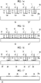
- Fig. 1 is a schematic perspective view illustrating a coating blade used for a method of producing a film according to an embodiment of the present invention
- Fig. 2 is a schematic view illustrating the coating blade used for the method of producing a film according to the embodiment of the present invention
- Fig. 3 is a view obtained by enlarging main parts of one end portion of the coating blade used for the method of producing a film according to the embodiment of the present invention
- Fig. 4 is a view obtained by enlarging main parts of the other end portion of the coating blade used for the method of producing a film according to the embodiment of the present invention.
- a coating blade 10 illustrated in Figs. 1 to 4 is used for forming a film 38 (see Fig. 8 ).
- a raw material solution 36 is held by a substrate 30, that is, a surface 30a of the substrate 30.
- the coating blade 10 includes, for example, a plane portion 12 formed of a rectangular flat plate and at least two side surfaces 14 provided on the plane portion 12.
- the plane portion 12 includes a facing surface 12a that faces the surface 30a of the substrate 30.
- two side surfaces 14 are provided in the periphery of the facing surface 12a.
- the longitudinal direction of the plane portion 12 is set as a first direction D1 and a direction orthogonal to the first direction D1 is set as a second direction D2 (see Fig. 1 ).
- the plane portion 12 is disposed so as to be spaced from the surface 30a of the substrate 30 in a state of facing the surface 30a, and the facing surface 12a of the plane portion 12 is inclined with respect to the surface 30a of the substrate 30.
- the facing surface 12a is an inclined surface which is monotonically inclined with respect to the surface 30a of the substrate 30.
- the facing surface 12a of the coating blade 10 may not be inclined with respect to the surface 30a of the substrate 30, and the facing surface 12a may be in parallel with the surface 30a of the substrate 30.
- a tilt angle ⁇ of the facing surface 12a of the coating blade 10 with respect to the surface 30a of the substrate 30 is an angle between the facing surface 12a of the coating blade 10 and the surface 30a of the substrate 30.
- the tilt angle ⁇ is preferably in a range of 1° to 6°.
- the tilt angle ⁇ is more preferably in a range of 3° to 5°.
- a proper amount of the raw material solution 36 can be held, and the mobility is high in a case of an organic semiconductor film, and thus the film 38 with an excellent film quality can be obtained.
- the length of the coating blade 10 is not particularly limited and is appropriately determined according to the length of a film to be formed.
- the length of the coating blade 10 is a length of the plane portion 12 in the longitudinal direction in Fig. 1 .
- the width of the coating blade 10 is not particularly limited and is appropriately determined according to the width of a film to be formed.
- the width of the coating blade 10 is a length of a direction orthogonal to the longitudinal direction described above, that is, the length of the second direction D2.
- Two side surfaces 14 of the coating blade 10 are respectively perpendicular to the surface 30a of the substrate 30 and provided so as to face each other.
- end surfaces 14b of the side surfaces 14 are disposed to face the surface 30a of the substrate 30.
- each end surface 14b of the side surface 14 and the surface 30a of the substrate 30 are disposed with a gap G 3 therebetween.
- a size d 3 of this gap G 3 is the same as a size d 2 of a second gap G 2 described below.
- a supply pipe 16 is provided on the plane portion 12.
- the raw material solution 36 is supplied through the supply pipe 16, and three surfaces which are the facing surface 12a and two side surfaces 14 of the coating blade 10 come into contact with the raw material solution 36.
- the surface tension is imparted to the raw material solution 36 due to the facing surface 12a and two side surfaces 14.
- the raw material solution 36 is held in a region surrounded by the plane portion 12 and the side surfaces 14, and a liquid reservoir 34 of the raw material solution 36 is formed.
- the liquid reservoir 34 is a region where the facing surface 12a and the side surfaces 14 of the coating blade 10 are in contact with the raw material solution 36.
- the facing surface 12a of the coating blade 10 is inclined, a first gap G 1 and the second gap G 2 having a difference in size between separation gaps are formed in the liquid reservoir 34 between the facing surface 12a of the coating blade 10 and the surface 30a of the substrate 30.
- a size d 1 of the first gap G 1 is larger than the size d 2 of the second gap G 2 .
- the first gap G 1 is a gap between the surface 30a of the substrate 30 and one end portion of the liquid reservoir 34 in the first direction D1.
- the second gap G 2 is a gap between the surface 30a and the substrate 30 and the other end portion of the liquid reservoir 34 in the first direction D1.
- the coating blade 10 is provided with two side surfaces 14 and includes an open part 33 formed such that at least a part in the periphery of the raw material solution 36 is opened. Specifically, in the coating blade 10, the first gap G 1 side between the facing surface 12a and the surface 30a of the substrate 30 is opened, and this opened side forms the open part 33.
- the size d 1 of the first gap G 1 indicates a length between a site 12c and the surface 30a of the substrate 30, which means from the site 12c at which a liquid surface 36a of the raw material solution 36 in the open part 33 of the liquid reservoir 34 is in contact with the facing surface 12a of the coating blade 10 to the surface 30a of the substrate 30 in a straight line La perpendicular to the surface 30a of the substrate 30.
- the size d 1 of the first gap G 1 decreases as the raw material solution 36 is dried and finally becomes the same as the size d 2 of the second gap G 2 , in a case where film formation is carried out by fixing the coating blade 10. Accordingly, the size d 1 of the first gap G 1 is a standard value at the time of supplying the raw material solution 36.
- the size d 1 of the first gap G 1 at the time of supplying the raw material solution depends on the length of a film to be formed which is in a range of 0.5 mm to 5 mm, the size d 1 is not limited.
- the size d 2 of the second gap G 2 is the minimum distance between the surface 30a of the substrate 30 in the liquid reservoir 34 and the facing surface 12a of the coating blade 10 and the value is 40 ⁇ m or less.
- the facing surface 12a of the coating blade 10 is monotonically inclined with respect to the surface 30a of the substrate 30 as described above. In this case, the length between the surface 30a of the substrate 30 and a corner portion 12d of the coating blade 10 illustrated in Fig. 4 becomes the minimum distance. Accordingly, in the coating blade 10 illustrated in Fig. 2 , the size d 2 of the second gap G 2 is the length between the surface 30a of the substrate 30 and the corner portion 12d of the coating blade 10.
- a range from the above-described site 12c to the above-described corner portion 12d in the facing surface 12a of the coating blade 10 is a range where the coating blade 10 is in contact with the raw material solution 36, and the range from the above-described site 12c to the above-described corner portion 12d is referred to as a solution holding portion.
- the size d 1 of the first gap G 1 is obtained by acquiring a digital image including the substrate 30 from the side surface of the coating blade 10, inputting this digital image into a computer, drawing the above-described straight line La on the digital image based on this digital image, and measuring the length between the site 12c of the facing surface 12a and the surface 30a of the substrate 30 on the computer.
- the size d 2 of the second gap G 2 is obtained by acquiring a digital image including the substrate 30 from the side surface of the coating blade 10, inputting this digital image into a computer, and measuring the length between the surface 30a of the substrate 30 and the corner portion 12d of the facing surface 12a of the coating blade 10 on the computer based on this digital image.
- the size d 2 of the second gap G 2 is 40 ⁇ m or less.
- the lower limit of the size d 2 of the second gap G 2 is 0 ⁇ m. In other words, film formation may be carried out in a grounded state. In a case where film formation is carried out by moving the coating blade 10 or the substrate 30, the lower limit of the size d 2 of the second gap G 2 is 10 ⁇ m.
- the size d 2 of the second gap G 2 is 40 ⁇ m or less, occurrence of vibration of the raw material solution 36 is suppressed so that the film quality of the film 38 can be improved.
- occurrence of vibration of the raw material solution 36 in the liquid reservoir 34 can be suppressed, and the moving speed can be increased. Therefore, for example, in a case where a thin film transistor is prepared, a transistor having excellent characteristics can be obtained with high productivity.
- the size d 2 of the second gap G 2 exceeds 40 ⁇ m, vibration of the raw material solution 36 in the liquid reservoir 34 occurs, and thus the film quality of the film 38 deteriorates. Consequently, for example, in a case where a thin film transistor is prepared, excellent characteristics cannot be obtained.
- the present invention is not limited to the above-described upper limits.
- the size d 3 of the gap G 3 is the same as the size d 2 of the second gap G 2 described above.
- the size d 3 of the gap G 3 is set to 40 ⁇ m or less, which is the same as the size d 2 of the second gap G 2 , the surface tension can be imparted to the raw material solution 36, and occurrence of vibration of the raw material solution 36 can be suppressed by the surface tension.
- the lower limit of the size d 3 of the gap G 3 is 0 ⁇ m. In other words, the film formation may be carried out in a grounded state. In a case where film formation is carried out by moving the coating blade 10 or the substrate 30, the lower limit of the size d 3 of the gap G 3 is 10 ⁇ m.
- the present invention is not limited to the above-described upper limit.
- the size d 3 of the gap G 3 is obtained by acquiring a digital image including the substrate 30 from the side surface of the coating blade 10, inputting this digital image into a computer, and measuring the length between the surface 30a of the substrate 30 and the bottom surface of the side surface 14 on the computer based on the digital image.
- the coating blade 10 is disposed on the surface 30a of the substrate 30 in a state in which the first gap G 1 , the second gap G 2 , and the gap G 3 described above are maintained, and the liquid reservoir 34 can be allowed to be present in a space between the facing surface 12a and the side surfaces 14 of the coating blade 10 and the surface 30a of the substrate 30 depending on the amount of the raw material solution 36 to be supplied.
- the liquid surface 36a of the raw material solution 36 is affected by the surface energy of the raw material solution 36, the surface energy of the facing surface 12a, and the surface energy of the side surfaces 14.
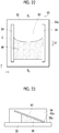
- Fig. 5 illustrates the liquid surface 36a of the raw material solution 36 in the open part 33 of the liquid reservoir 34.
- a film growth interface Bg is curved toward the center of the raw material solution 36.
- the film growth interface Bg indicates a surface where drying of the solvent in the raw material solution 36 progresses during the formation of the film 38 (see Fig. 8 ).
- the drying of the solvent in the raw material solution 36 advances along the first direction D1 described below, and the liquid surface 36a is moved to a contact side 13 along the progression of the drying. Therefore, the film growth interface Bg is the liquid surface 36a.
- the liquid surface 36a of the raw material solution 36 in the open part 33 is curved toward the center of the raw material solution 36.
- the curvature of the liquid surface 36a of the raw material solution 36 is caused by attraction of the raw material solution 36 to two side surfaces 14.
- the liquid surface 36a of the raw material solution 36 has a shape of a depression depressed to the contact side 13 in a plan view.
- the vibration of the raw material solution 36 is suppressed so that a film having a small film thickness can be obtained.
- the liquid surface 36a of the raw material solution 36 may protrude toward the center of the raw material solution 36.
- the liquid surface 36a has a shape of a projection projected to the open part 33 side in a plan view.
- the center of the raw material solution 36 indicates the center of gravity of the raw material solution 36.
- the liquid surface 36a is likely to have a shape of a projection in a plan view.
- the surface energy of the raw material solution 36 can be changed. Further, the surface energy of the facing surface 12a and the surface energy of the side surfaces 14 can be changed by performing an ultraviolet (UV) treatment, a plasma treatment, and the like. The surface energy can be changed using the material. Since particularly the side surfaces 14 impart the surface tension to the raw material solution 36, it is preferable that the wettability with respect to the raw material solution 36 and particularly with respect to the solvent is high. In this manner, the liquid surface 36a of the raw material solution 36 can be formed in a shape of a depression or a projection.
- UV ultraviolet
- each side surface 14 is set to be perpendicular to the surface 30a of the substrate 30, but the present invention is not limited to the right angle.
- the side surface 14 may be inclined with respect to the surface 30a of the substrate 30.
- the inclination of the side surface 14 is accepted to be 45° based on the right angle.
- the side surface 14 may be provided at 90° ⁇ 45° with respect to the surface 30a of the substrate 30. It is more efficient that the side surface 14 is perpendicular to the surface 30a of the substrate 30 from the viewpoint of the crystal formation area.
- the size d 3 of the gap G 3 described above and the size d 2 of the second gap G 2 described above are not necessarily the same as each other and may be different from each other.
- the side surfaces 14 are provided by extending in parallel with the first direction D1 as illustrated in Figs. 1 and 5 .
- the side surfaces 14 are provided by extending perpendicularly to the second direction.
- the inclination of each side surface 14 in the first direction D1 is accepted to be 30° based on the state in which the side surface 14 is in parallel with the first direction D1.
- the side surface 14 may be provided at a disposition angle of 90° ⁇ 30° with respect to the second direction D2.
- two side surfaces 14 are both provided at a disposition angle of 90°.
- the disposition angles of two side surfaces 14 in a case where the substrate 30 is viewed from the upper side of the surface 30a may not be necessarily the same as each other.
- the disposition angles of two side surfaces 14 may be symmetric or left-right asymmetric.
- the plane portion 12 and the side surfaces 14 of the coating blade 10 may be integrated or separated.
- the coating blade 10 is formed of glass, quartz glass, stainless steel, or the like.
- the substrate 30 for example, a glass substrate or a plastic substrate is used.
- a plastic substrate is formed of, for example, polyesters such as polyethylene terephthalate (PET) and polyethylene naphthalate (PEN); polyolefins such as polyethylene (PE), polypropylene (PP), polystyrene, ethylene vinyl acetate (EVA), a cycloolefin polymer (COP), and a cycloolefin copolymer (COC); a vinyl-based resin; and polycarbonate (PC), polyamide, polyimide, an acrylic resin, or triacetylcellulose (TAC).
- PET polyethylene terephthalate
- PEN polyethylene naphthalate
- polyolefins such as polyethylene (PE), polypropylene (PP), polystyrene, ethylene vinyl acetate (EVA), a cycloolefin polymer (COP), and a cycloolefin copolymer (COC)
- a vinyl-based resin and polycarbonate (PC), polyamide, polyimide
- Figs. 7 and 8 are schematic views sequentially illustrating steps in the formation step according to the first example of the method of producing a film of the embodiment of the present invention.
- the coating blade 10 is disposed on the surface 30a of the substrate 30 toward the side surfaces 14. At this time, the coating blade 10 is provided such that the tilt angle ⁇ , the first gap G 1 , the second gap G 2 , and the gap G 3 are set as described above. In this state, the raw material solution 36 is supplied, through the supply pipe 16, to a region surrounded by the surface 30a of the substrate 30, the facing surface 12a, and the side surfaces 14.
- the substrate 30 is held at an appropriate temperature according to the type of the raw material solution 36.
- the substrate temperature of the substrate 30 can be adjusted using, for example, a hot plate. Further, it is preferable that the raw material solution 36 is heated to the same temperature as the substrate temperature before being supplied. It is preferable that the supply pipe 16 is also appropriately heated.
- the film 38 is formed on the surface 30a of the substrate 30 as illustrated in Fig. 8 .
- the film 38 is formed by drying the solvent of the raw material solution 36 along a specific direction.
- the specific direction indicates the first direction D1 illustrated in Figs. 5 and 8 . In this manner, the high-quality film 38 having high uniformity, in which the alignment is aligned, can be obtained.
- the above-described specific direction indicates a direction in which drying of the solvent in the raw material solution 36 progresses, which is a direction in which the film 38 is formed. Further, the specific direction indicates a direction in which the film growth interface Bg, that is, the liquid surface 36a of the raw material solution 36 moves, and this specific direction is also referred to as a coating direction.
- the above-described specific direction is determined by, for example, the facing surface 12a of the plane portion 12 of the coating blade 10.
- the facing surface 12a of the plane portion 12 is close to the surface 30a of the substrate 30 and the corner portion 12d (see Fig. 4 ).
- the solvent of the raw material solution 36 is dried from the open part 33 toward the contact side 13 including the corner portion 12d (see Fig. 4 ). In other words, the solvent is dried along the first direction D1, and thus the film 38 is formed along the first direction D1.
- the surface tension is imparted to the raw material solution 36 by the side surfaces 14 as described above, but the side surfaces 14 do not affect the determination of the specific direction in the coating blade 10 illustrated in Fig. 1 .
- the specific direction described above is determined only by the facing surface 12a of the plane portion 12 of the coating blade 10.
- the determination of the specific direction is also affected by the side surfaces 14 in some cases depending on the shape and the size of the coating blade 10, the surface energy of the raw material solution 36, and the surface energy of the side surface 14.
- the surface tension can be imparted to the raw material solution 36 as described above.
- vibration of the raw material solution 36 occurs. Since the vibration of the raw material solution 36 is suppressed by the surface tension of the side surfaces 14 described above, continuous crystals can be prepared in a stabilized manner. Since the surface tension is imparted, it is preferable that the side surfaces 14 have high wettability with respect to the raw material solution 36 and particularly with respect to the solvent.
- the uniformity of the film quality in the film 38 can be increased.
- the uniformity of the film 38 indicates that unevenness in film thickness is small and a continuous crystal film is formed.
- the uniformity also indicates that the state of the film 38 is uniform, for example, the alignment direction is aligned over the entire film in a case of an alignment film and the crystal orientation is aligned over the entire film in a case of crystal orientation.
- the side surfaces 14 are present between a site where the raw material solution 36 is evaporated and the liquid reservoir 34 of the raw material solution 36. Therefore, practically, the vibration is unlikely to be transmitted to the raw material solution 36 inside the side surfaces 14. As the result, the vibration of the raw material solution 36 is suppressed.
- the evaporation of the solvent in the raw material solution 36 is suppressed by providing the side surfaces 14.
- the evaporation speed of the solvent is practically increased. This is because the raw material solution 36 also goes around the outside of the side surfaces 14 and then is evaporated due to the capillary phenomenon.
- An increase in evaporation speed leads to a reduction in film thickness of the film 38 of the organic semiconductor film or the like to be formed. As the result, the film 38 with a small film thickness can be obtained so that the thickness of the film 38 can be reduced.
- the configuration in which two side surfaces 14 are provided has been described, but the configuration is not limited thereto as long as at least one side surface 14 is provided.
- the high-quality film 38 having a small film thickness and high uniformity in film thickness or the like can be obtained.
- a coating method for obtaining a high-quality crystal film a method of using a coating blade inclined with respect to the surface 30a of the substrate 30 (hereinafter, also referred to as a "wedge method") has been suggested.
- the vibration of the raw material solution is suppressed by the surface tension while the substrate temperature is increased so that discontinuity such as step-cut of crystals is suppressed.
- the present invention is different from other techniques in terms that the surface tension can be further imparted to the raw material solution 36 by further providing side surfaces on the coating blade.
- the organic semiconductor is deposited on the outer periphery of a wall, but is different from the film such as an organic semiconductor film or the like described in the present invention.
- the edge cast method is a coating method of performing crystal growth toward glass which is an edge, but the crystal growth method for an organic semiconductor film described in the present invention is basically not a coating method of performing crystal growth toward the side surface.
- the crystal growth occurs perpendicular to the side surface 14 and the crystal growth is not performed toward the side surface 14.
- the substrate 30 in a case where the substrate 30 is present alone or a layer (not illustrated) is formed on the surface 30a of the substrate 30 and the film 38 (see Fig. 8 ) formed of an organic semiconductor material, a crystal material, or an alignment material is formed on the surface of the layer (not illustrated), the surface of the layer corresponds to the surface 30a of the substrate 30.
- Fig. 9 is a schematic cross-sectional view illustrating an example of a thin film transistor to be produced using the method of producing a film according to the embodiment of the present invention.
- the thin film transistor 40 illustrated in Fig. 9 is a bottom-gate top-contact type transistor.
- the thin film transistor 40 is provided such that a gate electrode 43 is formed on a surface 42a of a substrate 42.
- An insulating film 44 that covers this gate electrode 43 is formed on the surface 42a of the substrate 42.
- An organic semiconductor layer 46 is formed on a surface 44a of an insulating film 44. This organic semiconductor layer 46 is produced according to the method of producing a film.
- a source electrode 48a and a drain electrode 48b are formed on a surface 46a of the organic semiconductor layer 46.
- the organic semiconductor layer 46 is formed on the surface 44a of the insulating film 44.
- the surface 44a of the insulating film 44 corresponds to the surface 30a of the substrate 30 as described above.
- the maintenance of the film thickness of a crystal film to be small is a request in a case of a bottom-gate top-contact type transistor. Since the current path of a thin film transistor is in the vicinity of the interface between the insulating film and the organic semiconductor layer, the thickness of the organic semiconductor layer becomes a resistance component. Typically, it is desired that the thickness of the organic semiconductor layer is several tens of nanometers (several layers). However, as the thickness thereof is decreased, it becomes difficult to carry out film formation through coating.
- the organic semiconductor layer 46 which is an aligned continuous crystal film and has a small film thickness can be obtained. Therefore, a thin film transistor having high performance such as a high mobility can be obtained.
- a transistor on which the organic semiconductor film is formed according to the method of producing a film is not limited to the bottom-gate top-contact thin film transistor 40 illustrated in Fig. 9 .
- the transistor may be a bottom-gate bottom-contact type thin film transistor, a top-gate top-contact type thin film transistor, or a top-gate bottom-contact type thin film transistor.
- the method of producing a film can be used for producing various films, for example, a photoelectric conversion film and a photoelectric modulation film such as an organic solar cell, an electrooptic conversion film and an electrooptic modulation film such as an organic EL, a memory such as an organic ferroelectric memory, an organic conductive film, an inorganic conductive film, a polarizing film, an optical retardation film, a light guide, an optical amplification film, a gas sensor such as a volatile organic compound (VOC) sensor, a self-assembled film such as a block copolymer, a molecular alignment film, and a nanoparticle alignment film.
- a photoelectric conversion film and a photoelectric modulation film such as an organic solar cell
- an electrooptic conversion film and an electrooptic modulation film such as an organic EL
- a memory such as an organic ferroelectric memory
- an organic conductive film an inorganic conductive film, a polarizing film, an optical retardation film, a light guide, an optical
- Fig. 10 is a schematic cross-sectional view illustrating the first example of a position where a supply port of a supply pipe in the coating blade used for the method of producing a film according to the embodiment of the present invention is disposed.
- Fig. 11 is a schematic cross-sectional view illustrating a second example of a position where a supply port of a supply pipe in a coating blade is disposed.
- Fig. 12 is a schematic cross-sectional view illustrating a third example of a position where a supply port of a supply pipe in a coating blade is disposed.
- a supply port 16a of a supply pipe 16 in the plane portion 12 is flush with the facing surface 12a of the plane portion 12 illustrated in Fig. 10 , but the present invention is not limited to this configuration.
- the supply port 16a of the supply pipe 16 may protrude from the facing surface 12a of the plane portion 12 as illustrated in Fig. 11 or the supply port 16a of the supply pipe 16 may be depressed from the facing surface 12a of the plane portion 12 as illustrated in Fig. 12 and may be present inside the plane portion 12.
- the supply port 16a is used to supply the raw material solution 36.
- the position where the supply port 16a of the supply pipe 16 is disposed is not particularly limited.
- the supply port 16a thereof is disposed in two central sections from among four equal intervals obtained by dividing the length of the first direction D1 in which the liquid reservoir 34 as a region where the coating blade 10 is in contact with the above-described various raw material solutions 36 is projected on the surface 30a of the substrate 30.
- the region where the above-described liquid reservoir 34 is projected is a region from the above-described vertical straight line La to the corner portion 12d of the plane portion 12 in the coating blade 10 illustrated in Figs. 2 to 4 .
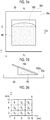
- Fig. 13 is a schematic view illustrating an example of disposition of a film to be formed according to the method of producing a film according to the embodiment of the present invention.
- Figs. 14 to 17 are schematic views sequentially illustrating steps in the second example of the method of producing a film according to the embodiment of the present invention.
- the same constituent elements as those in the coating blade 10 and the substrate 30 illustrated in Figs. 1 to 6 are denoted by the same reference numerals and the detailed description thereof will not be provided.
- Figs. 13 the same constituent elements as those in the coating blade 10 and the substrate 30 illustrated in Figs. 1 to 6 are denoted by the same reference numerals and the detailed description thereof will not be provided.
- Figs. 13 the same constituent elements as those in the coating blade 10 and the substrate 30 illustrated in Figs. 1 to 6 are denoted by the same reference numerals and the detailed description thereof will not be provided.
- Figs. 13 the same constituent elements as those in the coating blade 10 and the substrate 30 illustrated in
- the tilt angle ⁇ , the first gap G 1 , the second gap G 2 , and the gap G 3 are not illustrated, but the tilt angle ⁇ , the first gap G 1 , the second gap G 2 , and the gap G 3 are the same as those in the coating blade 10 illustrated in Fig. 1 .
- the film 38 can be formed in each of a plurality of regions 39 on the surface 30a of one substrate 30 illustrated in Fig. 13 .
- Each region 39 is a region where the film 38 is formed, and the regions are separated from one another and regularly arranged.
- the shapes and the areas of the regions 39 are the same.
- the film 38 to be formed in a plurality of regions 39 corresponds to, for example, the organic semiconductor layer 46 of the thin film transistor 40.
- the plurality of regions 39 are regularly arranged, but the arrangement of the plurality of regions 39 is appropriately determined depending on the target to be prepared and is not particularly limited to the regular arrangement.
- a coating head 50 including a plurality of coating blades 11 is used as illustrated in Fig. 14 .
- the plurality of coating blades 11 are arranged in a support 52 in the same manner as the arrangement of the regions 39 illustrated in Fig. 13 .
- the coating blade 11 is different from the coating blade 10 illustrated in Fig. 1 in terms of the configuration of the plane portion 12, but other configurations are the same as the configurations of the coating blade 10 illustrated in Fig. 1 .
- the plane portion 12 does not have a shape of a flat plate and is formed of a block-like member having the facing surface 12a.
- the plane portion 12 is attached to the support 52 in accordance with the positions of the regions 39.
- the supply pipe 16 is provided in each coating blade 11.
- the coating head 50 includes an elevating unit (not illustrated) which elevates and lowers the coating head 50; and a supply unit (not illustrated) which supplies the raw material solution 36 to the coating blade 11. Further, a heating unit (not illustrated) such as a hot plate which heats the substrate 30 and holds the increased temperature is also provided.
- the conditions for the substrate temperature and the like during the formation of the film 38 are the same as the conditions in the first example of the method of producing the film 38 illustrated in Figs. 7 and 8 .
- the coating head 50 is disposed such that the facing surfaces 12a are directed toward the surface 30a of the substrate 30.
- the coating blades 11 are provided on the surface 30a of the substrate 30 using an elevating unit (not illustrated) by bringing the coating head 50 closer to the surface 30a such that the tilt angle ⁇ , the first gap G 1 , the second gap G 2 , and the gap G 3 are set to be the same as described above as illustrated in Fig. 15 .
- the raw material solution 36 is supplied from the supply pipe 16 to a space between the facing surface 12a and the surface 30a of the substrate 30.
- the substrate 30 is heated, and the temperature thereof is maintained to a specific substrate temperature.
- the solvent in the raw material solution 36 is dried along a specific direction as described above, for example, along the first direction D1. In this manner, the film 38 is formed as illustrated in Fig. 16 .
- the coating head 50 is allowed to be spaced from the surface 30a of the substrate 30 using the elevating unit (not illustrated). As illustrated in Fig. 17 , a plurality of films 38 are formed on the surface 30a of the substrate 30.
- Fig. 18 is a schematic view illustrating the first example of a production device used for the method of producing a film according to the embodiment of the present invention.
- Fig. 19 is a schematic view for describing the third example of the method of producing a film according to the embodiment of the present invention.
- Fig. 20 is a plan view for describing the third example of the method of producing a film according to the embodiment of the present invention.
- a production device 60 illustrated in Fig. 18 is provided with a stage 64 in an inner portion 62a of a casing 62; a temperature controller 66 disposed on the stage 64; the coating blade 10; and a guide rail 74 which moves the coating blade 10 in the first direction D1 and the direction opposite to the first direction D1.
- the first direction D1 indicates the longitudinal direction of the plane portion 12 as described above.
- the stage 64 and the temperature controller 66 are connected to a driver 68, and movement of the substrate 30 by the stage 64 and control of the temperature of the substrate 30 by the temperature controller 66 are performed by the driver 68.
- the coating blade 10 is connected to a supply unit 72 through the supply pipe 16.
- the guide rail 74 is connected to a motor 78, and the motor 78 allows the coating blade 10 to move in the first direction D1 and the direction opposite to the first direction D1.
- the driver 68, the supply unit 72, and the motor 78 are connected to a control unit 79, and the driver 68, the supply unit 72, and the motor 78 are controlled by the control unit 79.
- the first direction D1 is aligned in a direction parallel to the surface of the stage 64. Accordingly, the direction opposite to the first direction D1 is also a direction parallel to the surface of the stage 64. Further, since the substrate 30 is disposed on the stage 64 such that the surface 30a of the substrate 30 is in parallel with the surface of the stage 64, the first direction D1 is a direction defined as a surface (not illustrated) parallel to the surface 30a of the substrate 30.
- the stage 64 is a place where the temperature controller 66 is disposed and the substrate 30 is further disposed thereon and is capable of moving the substrate 30 in the first direction D1 and the direction opposite to the first direction D1. Further, the stage 64 is capable of moving the substrate 30 in a second direction D2 (see Fig. 1 ) orthogonal to the first direction D1 and in a direction opposite to the second direction D2.
- the configuration of the stage 64 is not particularly limited as long as the substrate 30 can be moved in the first direction D1 and the direction opposite thereto, and the second direction D2 and the direction opposite thereto.
- the stage 64 may have a configuration of allowing the substrate 30 to move in a third direction D3 orthogonal to the first direction D1 and the second direction D2.
- the temperature controller 66 adjusts the temperature of the substrate 30 to a predetermined temperature and holds the temperature.
- the configuration of the temperature controller 66 is not particularly limited as long as the temperature of the substrate 30 can be set to a predetermined temperature as described above.
- a hot plate can be used as the temperature controller 66.
- the configuration of the supply pipe 16 connected to the coating blade 10 is not particularly limited as long as various solutions for forming a film described above can be supplied to a space between the facing surface 12a (see Fig. 2 ) of the coating blade 10 and the surface 30a of the substrate 30 from the supply unit 72. It is preferable that the supply pipe 16 has a flexibility so as to follow the coating blade 10 during the movement of the coating blade 10.
- the number of the supply pipes 16 is not limited to one, and a plurality of supply pipes 16 may be provided. The number thereof is appropriately determined depending on the size of the coating blade 10, the size of a film to be formed, and the like.
- the supply unit 72 is used to supply the raw material solution 36 to a space between the facing surface 12a (see Fig. 2 ) of the coating blade 10 and the surface 30a of the substrate 30 as described above and includes a tank (not illustrated) which stores the raw material solution 36; a pump (not illustrated) which sends the raw material solution 36 in the tank to the coating blade 10; and a flow meter (not illustrated) which measures the amount of the raw material solution 36 to be sent described above.
- a syringe pump can be used as the supply unit 72.
- the supply unit 72 and the supply pipe 16 are heated so that the temperature thereof is adjusted at an appropriate time.
- the temperature thereof is desirably set to approximately the same temperature as the substrate temperature.
- the raw material solution 36 can be stably supplied by reliably dissolving the raw material solution 36 for forming a film through the heating. Further, as a difference in temperature between the raw material solution 36 and the substrate 30 at the time of being supplied is decreased, the stabilized liquid reservoir 34 (see Fig. 2 ) can be formed.
- the coating blade 10 is provided with a sensor 70 which measures the distance between the surface 30a of the substrate 30 to be disposed on the temperature controller 66 and the facing surface 12a (see Fig. 2 ) of the coating blade 10 (see Fig. 2 ).
- the sensor 70 is connected to the control unit 79 so that the driver 68, the supply unit 72, and the motor 78 are controlled by the control unit 79 based on the distance between the surface 30a of the substrate 30 and the facing surface 12a (see Fig. 2 ) of the coating blade 10 (see Fig. 2 ).
- the configuration of the sensor 70 is not particularly limited as long as the above-described distance can be measured, and the distance thereof is measured using, for example, an optical measuring method.
- As the sensor 70 a sensor using light interference, a sensor using the confocus, or a sensor using laser light can be appropriately used.
- a carriage 76 is attached to the guide rail 74.
- the carriage 76 can be moved in the first direction D1 and the direction opposite to the first direction D1 by the guide rail 74, and the coating blade 10 is moved in the first direction D1 and the direction opposite to the first direction D1 together with the carriage 76.
- the carriage 76 is moved in the first direction D1 and the direction opposite to the first direction D1 by the motor 78.
- the position of the carriage 76 can be calculated based on read values of a linear scale (not illustrated) provided on the guide rail 74, and thus the position of the coating blade 10 in the first direction D1 can be calculated.
- the carriage 76 is capable of changing the height at which the coating blade 10 has been attached and the tilt angle ⁇ .
- the moving speed of the facing surface 12a (see Fig. 2 ) of the coating blade 10 is adjusted by the motor 78.
- the coating blade 10 can be moved in the first direction D1 and the direction opposite to the first direction D1
- the substrate 30 can be moved in the first direction D1 and the direction opposite to the first direction D1.
- the size d 2 of the second gap G 2 is measured based on the amount of the carriage 76 to be elevated in a state in which the facing surface 12a of the coating blade 10 is brought into contact with the surface 30a of the substrate 30.
- the size d 2 of the second gap G 2 can be measured in a case where a micrometer (not illustrated) for adjusting the height is provided in the carriage 76.
- the size d 1 of the first gap G 1 can be calculated based on the length of the coating blade 10 in a case where the tilt angle ⁇ of the coating blade 10 is known.
- the length of the coating blade 10 is the length of the plane portion 12 in the longitudinal direction.
- the facing surface 12a of the coating blade 10 is disposed on the surface 30a of the substrate 30 such that the facing surface 12a is inclined at a tilt angle ⁇ in a state in which the first gap G 1 , the second gap G 2 , and the gap G 3 described above are provided.
- the raw material solution 36 is supplied to the liquid reservoir 34 through the supply pipe 16 from the supply unit 72 (see Fig. 18 ).
- the substrate temperature of the substrate 30 is set to a predetermined temperature using the above-described temperature controller 66 (see Fig. 18 ).
- the substrate 30 is moved in a direction D B from the coating blade 10 at a predetermined moving speed in a state in which the facing surface 12a of the coating blade 10 is in contact with the raw material solution 36 as illustrated in Figs. 19 and 20 while the raw material solution 36 is supplied to a space between the coating blade 10 and the surface 30a of the substrate 30, that is, the liquid reservoir 34.
- the region where the liquid surface 36a of the raw material solution 36 of the open part 33 is in contact with the surface 30a of the substrate 30 becomes a crystal growth portion Cg (see Fig. 19 ) serving as a starting point where the film 38 is formed, and the film 38 is sequentially formed from this crystal growth portion Cg in a direction D F . Therefore, the film 38 is continuously formed in the direction D F while the raw material solution 36 is applied to the direction D F in which the coating blade 10 is moved.
- direction D B is a direction toward the open part 33 from the center of the raw material solution 36, which is the same direction as the direction opposite to the first direction D1 described above.
- direction D F is a direction opposite to the direction D B , which is the same direction as the first direction D1.
- the lower limit of the size d 2 of the second gap G 2 is 10 ⁇ m as described above, and the lower limit of the size d 3 of the gap G 3 is 10 ⁇ m. Since the film formation is carried out while the raw material solution 36 is supplied, the film formation can be made in a state in which the size d 1 of the first gap G 1 is not changed. In addition, the size d 1 of the first gap G 1 may be changed. Even in a case where a film is continuously formed, the size d 2 of the second gap G 2 and the size d 3 of the gap G 3 may be the same as or different from each other.
- the amount of the raw material solution 36 to be supplied is appropriately determined according to the temperature and the moving speed of the substrate 30, the size of the film 38 to be formed, and the like.
- the crystal growth portion Cg can be specified by acquiring a digital image including the liquid reservoir 34 and the film 38, inputting this digital image into a computer, and visually observing the vicinity of the boundary between the liquid reservoir 34 and the film 38 based on this digital image.
- the method of continuously forming the film 38 by moving the substrate 30 in the direction D B has been described, but the present invention is not limited thereto.
- the film 38 can be continuously formed in the direction D F as described above by moving the coating blade 10 in the direction D F at a predetermined moving speed.
- the substrate temperature Ts is held to a temperature satisfying an expression "Tb - 50°C ⁇ Ts ⁇ Tb" according to any method of producing the film 38 described above.
- the substrate temperature is in the above-described temperature range, evaporation of the solvent in the raw material solution 36 is promoted, and the film formation speed for the film 38 can be increased. Therefore, the productivity of the film 38 can be increased.
- the substrate temperature Ts during the formation of the film 38 satisfies an expression "Tb - 20°C ⁇ Ts ⁇ Tb". Further, the substrate temperature Ts indicates the temperature of the surface 30a of the substrate 30.
- the moving speed of the substrate 30 during the formation of the film 38 is preferably 5 mm/min or greater and more preferably 10 mm/min or greater.
- the film 38 can be formed at a high film formation speed and the productivity can be increased.
- the upper limit of the moving speed described above is approximately 100 mm/min, and an organic semiconductor film with excellent crystallinity as the film 38 and a high mobility can be obtained in a case where the above-described moving speed is 100 mm/min or less.
- the film 38 is formed, for example, in an atmosphere under atmospheric pressure.
- the distance between the facing surface 12a of the coating blade 10 and the surface 30a of the substrate 30 is measured by the sensor 70 (see Fig. 18 ), the first gap G 1 , the second gap G 2 , and the gap G 3 are maintained, and the substrate 30 is moved in the direction D B .
- the production device 60 is of a single wafer type, but the method of producing a film is not limited to the single wafer type, and a roll-to-roll type production device as a production device 60a illustrated in Fig. 21 may be employed.
- the production device 60a illustrated in Fig. 21 is different from the production device 60 illustrated in Fig. 18 in terms that the stage 64 is not provided, the transport form of the substrate 30 is stretched to an unwinding roll 80 and a winding roll 82, the coating blade 10 is disposed on the surface 30a side of the substrate 30 as described above, and the temperature controller 66 is disposed on a rear surface 30b side.
- the configurations other than these are the same as the configurations of the production device 60 illustrated in Fig. 18 .
- the substrate temperature is set to a predetermined temperature by the temperature controller 66 so that the film 38 is formed by the coating blade 10. Further, during the film formation of the film 38, the substrate 30 may be transported by being wound up using the winding roll 82, and the coating blade 10 may be moved.
- the above-described raw material solution 36 for forming a film is, for example, a solution containing a material having an aligning property.
- the solution containing a material having an aligning property is, for example, a solution containing a material that forms a crystal or a solution containing an organic semiconductor.
- the organic semiconductor may be not only a transistor but also an organic solar cell material.
- Examples of the material having a crystallinity include an organic ferroelectric material such as croconic acid or an imidazole compound; and a gas sensor material such as a pyrrole imine-naphthalene diimide (PI-NDI) compound.
- PI-NDI pyrrole imine-naphthalene diimide
- the solution containing an organic semiconductor used for the raw material solution 36 typically contains at least an organic semiconductor (organic semiconductor compound) and a solvent.
- the type of the organic semiconductor is not particularly limited, and a known organic semiconductor can be used. Specific examples thereof include pentacenes such as 6,13-bis(triisopropylsilylethynyl)pentacene (TIPS pentacene), tetramethyl pentacene, and perfluoropentacene; anthradithiophenes such as TES-ADT (5,11-bis(triethylsilylethynyl)anthradithiophene), and diF-TES-ADT (2,8-difluoro-5,11-bis(triethylsilylethynyl)anthradithiophene); benzothienobenzothiophenes such as DPh-BTBT (2,7-dipheny1[1]benzothieno[3,2-b][1]benzothiophene) and Cn-BTBT (benzothienobenzothiophene); dinaphthothienothi
- the type of the solvent is not particularly limited, and examples thereof include alcohol-based solvents such as methanol and ethanol; ketone-based solvents such as acetone, methyl ethyl ketone, and methyl isobutyl ketone; aromatic solvents such as benzene and thiophene, and halogen (chlorine, bromine, or the like) substituted substances (halogenated aromatic solvents) thereof; ether-based solvents such as tetrahydrofuran and diethyl ether; amide-based solvents such as dimethylformamide and dimethylacetamide; and sulfonic acid-based solvents such as dimethyl sulfoxide and sulfolane.
- alcohol-based solvents such as methanol and ethanol
- ketone-based solvents such as acetone, methyl ethyl ketone, and methyl isobutyl ketone
- aromatic solvents such as benzene and thiophene, and halogen
- the present invention is basically configured as described above.
- the method of producing a film according to the embodiment of the present invention has been described in detail, but the present invention is not limited to the above-described embodiments, and various improvements and modifications can also be made within the range not departing from the scope of the present invention.
- organic semiconductor layers respectively formed of an organic semiconductor film were formed according to the method of producing a film, thereby obtaining thin film transistors of Examples 1 to 20 and Comparative Example 1.
- the film thicknesses and the thin film transistor element characteristics were evaluated.
- the thin film transistors in Examples 3 to 20 the thin film transistor element characteristics were evaluated.
- Each thin film transistor was prepared in the following manner by setting the channel width to 1 mm and the channel length to 50 ⁇ m using the bottom-gate top-contact type thin film transistor 40 illustrated in Fig. 9 .
- a gate pattern was prepared through vacuum deposition using a metal mask. Chromium (Cr) having a thickness of 10 nm was deposited as an adhesive layer to form a gate electrode having a thickness of 40 nm using silver (Ag).
- a polyimide insulating film having a thickness of 0.5 ⁇ m was formed by spin-coating the glass substrate and curing the resultant.
- the glass substrate was provided on a hot plate present on a stage, the temperature of the surface of the substrate was set to 100°C, 120°C, or 140°C, and the surface thereof was coated with the raw material solution described below to form an organic semiconductor film, thereby obtaining an organic semiconductor layer.
- Slide glass was used as the coating blade.
- the height of the slide glass with respect to the surface of the glass substrate was adjusted such that the tilt angle was set to be in a range of 1° to 6°.
- the raw material solution whose concentration was adjusted to be in a range of 0.05% to 0.3% by mass was supplied to a space below the coating blade such that the length was set to be in a range of 10 to 20 mm.
- a glass material having a rectangular parallelepiped shape was provided as the side surface.
- a glass material having a size of 20 mm ⁇ 5 mm ⁇ 2 mm was used as the glass material.
- the amount of the raw material solution was reduced due to evaporation toward the coating blade and a contact side 92a (see Fig. 23 ) of the substrate in a state in which the coating blade was allowed to stand on the glass substrate and the position thereof was fixed so that an organic semiconductor film was formed.
- anisole was used as the solvent using C4-TBBT (thieno[3,2-f:4,5-f']bis[1]benzothiophene) as the organic semiconductor.
- the raw material solution was obtained by heating and dissolving anisole such that the concentration of the above-described organic semiconductor was set to 0.1% by mass.
- a gold (Au) film having a thickness of 70 nm was formed on the organic semiconductor layer as a source drain electrode according to a vacuum deposition method performed using a metal mask.
- the position of the electrode was adjusted such that a thin film transistor was prepared in the vicinity of the center of the organic semiconductor with respect to the coating width thereof.
- the coating blade was provided at a tilt angle of 4° using slide glass having a width of 18 mm.
- the substrate temperature was set to 120°C.
- the solution concentration of the raw material solution was examined while being adjusted such that a high-quality film having a concentration of 0.05% to 0.3% by mass was able to be obtained.
- the raw material solution was introduced up to the extent that the solution length was 12 mm.
- the value of the solution length is a value of the y axis in Fig. 26 .
- the numerical value of the solution length was set to a value of the length in a Y direction parallel to the first direction D1.
- the width was set to a value of the length in an X direction orthogonal to the Y direction.
- Example 1 has a configuration illustrated in Figs. 22 and 23 , and a coating blade 90 was configured to include a plane portion 92 and side surfaces 94.
- a reference numeral 92a in Fig. 23 represents a contact side.
- Fig. 23 is a cross-sectional view taken along a line B 1 -B 2 of Fig. 22 .
- Example 2 an ultraviolet (UV) treatment was performed on the glass material of the side surface of the coating blade.
- Comparative Example 1 has a configuration illustrated in Figs. 24 and 25 , and a coating blade 100 was configured to have only a plane portion 102 and was not provided with a glass material on the side surface thereof.
- a reference numeral 102a in Fig. 25 represents a contact side.
- Fig. 25 is a cross-sectional view taken along a line A 1 -A 2 of Fig. 24 .
- the coating blade was provided at a tilt angle of 1° to 6° using slide glass having a width of 18 mm.
- the substrate temperature was set to 100°C, 120°C, or 140°C.
- the solution concentration of the raw material solution was examined while being adjusted such that a high-quality film having a concentration of 0.05% to 0.3% by mass was able to be obtained.
- the raw material solution was introduced up to the extent that the solution length was 12 mm.
- the value of the solution length is a value of the y axis in Fig. 26 .
- the saturation mobility of each of nine regions S 1 to S 9 illustrated in Fig. 26 was measured in the same manner as in Example 1, Example 2, and Comparative Example 1, the measured values were averaged, and the thin film transistor element characteristics were evaluated based on the average value, as described below.
- Example 1 The film thicknesses and the thin film transistor element characteristics of Example 1, Example 2, and Comparative Example 1 are listed in Table 1 below.
- the thin film transistor element characteristics of Examples 3 to 20 are listed in Table 2 below.
- TFT characteristics are noted as "TFT characteristics”.
- the film thickness of the formed organic semiconductor film was obtained by dividing the region S illustrated in Fig. 26 into a total of nine regions S 1 to S 9 , and measuring the film thickness of each of the regions S 1 to S 9 .
- a stylus type step profiler (DEKTAK) was used for measuring the film thickness of the organic semiconductor film.
- the region S was set to have the same range.
- the range of the region S illustrated in Figs. 22 and 24 was set to have a size of 12 mm in the y direction and a size of 18 mm in the x direction.
- the saturation mobility of each of the prepared thin film transistors was measured using a semiconductor parameter analyzer (manufactured by Agilent Technologies, Inc., 4156C) The saturation mobility was obtained by dividing the region S illustrated in Fig. 26 into a total of nine regions S 1 to S 9 similar to the measurement of the film thickness and measuring the saturation mobility of each of the regions S 1 to S 9 .
- the thin film transistor element characteristics were evaluated based on the measured saturation mobilities ⁇ and the following evaluation standard.
- Example 1 and Example 2 the film thickness was thin and unevenness in film thickness was small so that a uniform film was obtained, compared to Comparative Example 1.
- unevenness in saturation mobility was small and the saturation mobility was uniform. Therefore, the TFT characteristics were excellent.
- Example 1 and Example 2 the film thickness was uniform and the uniformity was high so that a high-quality film with excellent TFT characteristics was able to be obtained.
- the UV treatment was performed on the side surfaces, and thus the wettability of the side surfaces with respect to the raw material solution was higher than that of the side surfaces of Example 1. Therefore, both of the uniformity in film thickness and the uniformity in TFT characteristics were excellent.
- Fig. 27 illustrates the film of Example 1
- Fig. 28 illustrates the film of Comparative Example 1.
- Figs. 27 and 28 are both photomicrographs obtained by a polarizing microscope.
- the uniform film 38 was obtained in Example 1 as illustrated in Fig. 27 , but the film 38 which had partially turbid regions 104 and was nonuniform as illustrated in Fig. 28 was formed in Comparative Example 1.
- the turbid regions 104 were regions where the film thickness was not uniform, the crystal was discontinuous, and the alignment was not made. It was considered that the turbid regions 104 were generated due to extra nucleation caused by repetitive evaporation and dissolution of the raw material solution because side surfaces were not provided.
- the substrate temperatures were 100°C, 120°C, and 140°C, and in a case where the tilt angle was in a range of 3° to 5° regardless of the substrate temperature, the saturation mobility was further increased and excellent TFT characteristics were obtained.
- the length of the solution supplied initially was in a range of 10 to 20 mm, which means that the same tendency was obtained.
Landscapes
- Engineering & Computer Science (AREA)
- Manufacturing & Machinery (AREA)
- Chemical & Material Sciences (AREA)
- Crystallography & Structural Chemistry (AREA)
- Materials Engineering (AREA)
- Liquid Deposition Of Substances Of Which Semiconductor Devices Are Composed (AREA)
- Thin Film Transistor (AREA)
- Application Of Or Painting With Fluid Materials (AREA)
Abstract
Description
- The present invention relates to a method of producing a film according to a coating method and particularly relates to a method of producing a film formed of an organic semiconductor material, a crystal material, an alignment material, and the like.
- Currently, organic semiconductors have been expected as a semiconductor material used for flexible devices and the like. One of the features of organic semiconductors is that the organic semiconductors can be formed by performing coating at a low temperature, compared to inorganic semiconductors such as silicon. Various methods of producing an organic semiconductor film obtained by using organic semiconductors have been suggested.
-
JP5397921B - According to the method of producing an organic semiconductor film in
JP5397921B -
WO2016/031968A describes a method of producing a semiconductor film.WO2016/031968A describes an edge cast method of coating a surface of a gate insulating film formed on a gate electrode. - According to the edge cast method, a nozzle and a blade are disposed on the gate insulating film. A coating solution is supplied from the nozzle to an edge portion facing the surface of the gate insulating film on which the blade is disposed. The nozzle and the substrate are held at a temperature at which the solvent is evaporated. The substrate is moved in one direction while the coating solution is continuously supplied such that the amount of the coating solution held by the edge portion becomes constant. The organic semiconductor material is crystallized as the solvent in the coating solution supplied from the nozzle is evaporated.
- An organic semiconductor film can be formed using any of the method of producing an organic semiconductor film in
JP5397921B WO2016/031968A . However, in regard to an organic semiconductor film, further reduction in film thickness and uniformity in film thickness or the like have been required currently. - An object of the present invention is to solve the problems caused by the techniques of the related art described above and to provide a method of producing a high-quality film having a thin film and high uniformity in film thickness or the like.
- In order to achieve the above-described object, the present invention provides a method of producing a film, comprising: supplying a raw material solution containing a solvent and a material that forms a film onto a substrate and drying the solvent to form the film on the substrate, in which a coating blade holding the raw material solution on the substrate is used, the coating blade has a facing surface which faces a surface of the substrate and at least one side surface which is provided in the periphery of the facing surface and is in contact with the raw material solution, and the solvent of the raw material solution is dried along a specific direction to form the film.
- It is preferable that at least three surfaces, which are the facing surface and two side surfaces of the coating blade, are in contact with the raw material solution.
- Further, it is preferable that the specific direction in which the raw material solution is dried is determined by at least one surface from among the facing surface and at least two side surfaces of the coating blade.
- Further, it is preferable that the specific direction in which the raw material solution is dried is determined only by one surface from among the facing surface and at least two side surfaces of the coating blade. Further, it is preferable that the specific direction in which the raw material solution is dried is determined only by the facing surface of the coating blade.
- It is preferable that the coating blade has two side surfaces, and two side surfaces are respectively perpendicular to the surface of the substrate and provided so as to face each other.
- It is preferable that the facing surface of the coating blade is inclined with respect to the surface of the substrate. It is preferable that a tilt angle of the facing surface of the coating blade with respect to the surface of the substrate is in a range of 1° to 6°.
- It is preferable that a film growth interface of the raw material solution held on the substrate by the coating blade is curved toward the center of the raw material solution.
- Further, it is preferable that a position of the coating blade is fixed to the surface of the substrate.
- The coating blade may include an open part that opens at least a part in the periphery of the raw material solution and the substrate may be moved in a direction toward the open part from the center of the raw material solution.
- In this case, it is preferable that the substrate is moved while the raw material solution is supplied to a space between the surface of the substrate and the coating blade so that the film is continuously formed.
- It is preferable that, in a case where a boiling point of the solvent of the raw material solution is set as Tb°C and a substrate temperature is set as Ts°C, the substrate temperature Ts is held at a temperature satisfying an expression of "Tb - 50°C ≤ Ts ≤ Tb".
- The film is formed of a material having an aligning property. For example, the material having an aligning property is a material or an organic semiconductor that forms a crystal.
- According to the present invention, it is possible to obtain a high-quality film having a thin film and high uniformity in film thickness or the like.
-
-
Fig. 1 is a schematic perspective view illustrating a coating blade used for a method of producing a film according to an embodiment of the present invention. -
Fig. 2 is a schematic view illustrating the coating blade used for the method of producing a film according to the embodiment of the present invention. -
Fig. 3 is a view obtained by enlarging main parts of one end portion of the coating blade used for the method of producing a film according to the embodiment of the present invention. -
Fig. 4 is a view obtained by enlarging main parts of the other end portion of the coating blade used for the method of producing a film according to the embodiment of the present invention. -
Fig. 5 is a schematic plan view illustrating the coating blade used for the method of producing a film according to the embodiment of the present invention. -
Fig. 6 is a schematic view illustrating a side surface of the coating blade used for the method of producing a film according to the embodiment of the present invention. -
Fig. 7 is a schematic view illustrating one step in a first example of the method of producing a film according to the embodiment of the present invention. -
Fig. 8 is a schematic view illustrating one step in the first example of the method of producing a film according to the embodiment of the present invention. -
Fig. 9 is a schematic cross-sectional view illustrating an example of a thin film transistor to be produced using the method of producing a film according to the embodiment of the present invention. -
Fig. 10 is a schematic cross-sectional view illustrating a first example of a position where a supply port of a supply pipe in the coating blade used for the method of producing a film according to the embodiment of the present invention is disposed. -
Fig. 11 is a schematic cross-sectional view illustrating a second example of the position where the supply port of the supply pipe in the coating blade is disposed. -
Fig. 12 is a schematic cross-sectional view illustrating a third example of the position where the supply port of the supply pipe in the coating blade is disposed. -
Fig. 13 is a schematic view illustrating an example of disposition of a film to be formed according to the method of producing a film according to the embodiment of the present invention. -
Fig. 14 is a schematic view illustrating one step in a second example of the method of producing a film according to the embodiment of the present invention. -
Fig. 15 is a schematic view illustrating one step in the second example of the method of producing a film according to the embodiment of the present invention. -
Fig. 16 is a schematic view illustrating one step in the second example of the method of producing a film according to the embodiment of the present invention. -
Fig. 17 is a schematic view illustrating one step in the second example of the method of producing a film according to the embodiment of the present invention. -
Fig. 18 is a schematic view illustrating a first example of a production device used for the method of producing a film according to the embodiment of the present invention. -
Fig. 19 is a schematic view for describing a third example of the method of producing a film according to the embodiment of the present invention. -
Fig. 20 is a plan view for describing the third example of the method of producing a film according to the embodiment of the present invention. -
Fig. 21 is a schematic view illustrating a second example of the production device used for the method of producing a film according to the embodiment of the present invention. -
Fig. 22 is a schematic view illustrating a coating blade used in an example. -
Fig. 23 is a schematic cross-sectional view illustrating the coating blade used in the example. -
Fig. 24 is a schematic view illustrating a coating blade used in a comparative example. -
Fig. 25 is a schematic cross-sectional view illustrating the coating blade used in the comparative example. -
Fig. 26 is a schematic view showing a measuring region of a film thickness and a saturation mobility. -
Fig. 27 is a schematic view showing the film in Example 1. -
Fig. 28 is a schematic view showing the film in Comparative Example 1. - Hereinafter, a method of producing a film according to the embodiment of the present invention will be described in detail based on preferred embodiments illustrated in the accompanying drawings.
- Further, hereinafter, "to" indicating the ranges of numerical values includes numerical values described on both sides. For example, the expression "ε is in a range of a numerical value α to a numerical value β" means that the range of ε is a range including the numerical value α and the numerical value β and satisfies an expression "α ≤ ε ≤ β" shown using the mathematical symbols.
- Angles such as "an angle represented by a specific numerical value", "parallel", "perpendicular", and "orthogonal" include error ranges typically accepted in the corresponding technical fields unless otherwise specified.
-
Fig. 1 is a schematic perspective view illustrating a coating blade used for a method of producing a film according to an embodiment of the present invention,Fig. 2 is a schematic view illustrating the coating blade used for the method of producing a film according to the embodiment of the present invention,Fig. 3 is a view obtained by enlarging main parts of one end portion of the coating blade used for the method of producing a film according to the embodiment of the present invention, andFig. 4 is a view obtained by enlarging main parts of the other end portion of the coating blade used for the method of producing a film according to the embodiment of the present invention. - A
coating blade 10 illustrated inFigs. 1 to 4 is used for forming a film 38 (seeFig. 8 ). Araw material solution 36 is held by asubstrate 30, that is, asurface 30a of thesubstrate 30. - The
coating blade 10 includes, for example, aplane portion 12 formed of a rectangular flat plate and at least twoside surfaces 14 provided on theplane portion 12. - The
plane portion 12 includes a facingsurface 12a that faces thesurface 30a of thesubstrate 30. For example, twoside surfaces 14 are provided in the periphery of the facingsurface 12a. InFigs. 1 to 4 , the longitudinal direction of theplane portion 12 is set as a first direction D1 and a direction orthogonal to the first direction D1 is set as a second direction D2 (seeFig. 1 ). - In the
coating blade 10, theplane portion 12 is disposed so as to be spaced from thesurface 30a of thesubstrate 30 in a state of facing thesurface 30a, and the facingsurface 12a of theplane portion 12 is inclined with respect to thesurface 30a of thesubstrate 30. For example, the facingsurface 12a is an inclined surface which is monotonically inclined with respect to thesurface 30a of thesubstrate 30. - Further, the facing
surface 12a of thecoating blade 10 may not be inclined with respect to thesurface 30a of thesubstrate 30, and the facingsurface 12a may be in parallel with thesurface 30a of thesubstrate 30. - A tilt angle θ of the facing
surface 12a of thecoating blade 10 with respect to thesurface 30a of thesubstrate 30 is an angle between the facingsurface 12a of thecoating blade 10 and thesurface 30a of thesubstrate 30. - For example, the tilt angle θ is preferably in a range of 1° to 6°. The tilt angle θ is more preferably in a range of 3° to 5°. In a case where the tilt angle θ is in a range of 1° to 6°, a proper amount of the
raw material solution 36 can be held, and the mobility is high in a case of an organic semiconductor film, and thus thefilm 38 with an excellent film quality can be obtained. - The length of the
coating blade 10 is not particularly limited and is appropriately determined according to the length of a film to be formed. The length of thecoating blade 10 is a length of theplane portion 12 in the longitudinal direction inFig. 1 . - The width of the
coating blade 10 is not particularly limited and is appropriately determined according to the width of a film to be formed. The width of thecoating blade 10 is a length of a direction orthogonal to the longitudinal direction described above, that is, the length of the second direction D2. - Two side surfaces 14 of the
coating blade 10 are respectively perpendicular to thesurface 30a of thesubstrate 30 and provided so as to face each other. In thecoating blade 10, end surfaces 14b of the side surfaces 14 are disposed to face thesurface 30a of thesubstrate 30. At this time, eachend surface 14b of theside surface 14 and thesurface 30a of thesubstrate 30 are disposed with a gap G3 therebetween. A size d3 of this gap G3 is the same as a size d2 of a second gap G2 described below. - In the
coating blade 10, asupply pipe 16 is provided on theplane portion 12. Theraw material solution 36 is supplied through thesupply pipe 16, and three surfaces which are the facingsurface 12a and twoside surfaces 14 of thecoating blade 10 come into contact with theraw material solution 36. The surface tension is imparted to theraw material solution 36 due to the facingsurface 12a and two side surfaces 14. For example, it is preferable that at least three surfaces which are the facingsurface 12a and twoside surfaces 14 of thecoating blade 10 are in contact with theraw material solution 36. - In the
coating blade 10, theraw material solution 36 is held in a region surrounded by theplane portion 12 and the side surfaces 14, and aliquid reservoir 34 of theraw material solution 36 is formed. Theliquid reservoir 34 is a region where the facingsurface 12a and the side surfaces 14 of thecoating blade 10 are in contact with theraw material solution 36. - The facing
surface 12a of thecoating blade 10 is inclined, a first gap G1 and the second gap G2 having a difference in size between separation gaps are formed in theliquid reservoir 34 between the facingsurface 12a of thecoating blade 10 and thesurface 30a of thesubstrate 30. A size d1 of the first gap G1 is larger than the size d2 of the second gap G2. - The first gap G1 is a gap between the
surface 30a of thesubstrate 30 and one end portion of theliquid reservoir 34 in the first direction D1. The second gap G2 is a gap between thesurface 30a and thesubstrate 30 and the other end portion of theliquid reservoir 34 in the first direction D1. Thecoating blade 10 is provided with twoside surfaces 14 and includes anopen part 33 formed such that at least a part in the periphery of theraw material solution 36 is opened. Specifically, in thecoating blade 10, the first gap G1 side between the facingsurface 12a and thesurface 30a of thesubstrate 30 is opened, and this opened side forms theopen part 33. - As illustrated in
Fig. 3 , the size d1 of the first gap G1 indicates a length between asite 12c and thesurface 30a of thesubstrate 30, which means from thesite 12c at which aliquid surface 36a of theraw material solution 36 in theopen part 33 of theliquid reservoir 34 is in contact with the facingsurface 12a of thecoating blade 10 to thesurface 30a of thesubstrate 30 in a straight line La perpendicular to thesurface 30a of thesubstrate 30. - The size d1 of the first gap G1 decreases as the
raw material solution 36 is dried and finally becomes the same as the size d2 of the second gap G2, in a case where film formation is carried out by fixing thecoating blade 10. Accordingly, the size d1 of the first gap G1 is a standard value at the time of supplying theraw material solution 36. - Since the size d1 of the first gap G1 at the time of supplying the raw material solution depends on the length of a film to be formed which is in a range of 0.5 mm to 5 mm, the size d1 is not limited.
- The size d2 of the second gap G2 is the minimum distance between the
surface 30a of thesubstrate 30 in theliquid reservoir 34 and the facingsurface 12a of thecoating blade 10 and the value is 40 µm or less. The facingsurface 12a of thecoating blade 10 is monotonically inclined with respect to thesurface 30a of thesubstrate 30 as described above. In this case, the length between thesurface 30a of thesubstrate 30 and acorner portion 12d of thecoating blade 10 illustrated inFig. 4 becomes the minimum distance. Accordingly, in thecoating blade 10 illustrated inFig. 2 , the size d2 of the second gap G2 is the length between thesurface 30a of thesubstrate 30 and thecorner portion 12d of thecoating blade 10. A range from the above-describedsite 12c to the above-describedcorner portion 12d in the facingsurface 12a of thecoating blade 10 is a range where thecoating blade 10 is in contact with theraw material solution 36, and the range from the above-describedsite 12c to the above-describedcorner portion 12d is referred to as a solution holding portion. - The size d1 of the first gap G1 is obtained by acquiring a digital image including the
substrate 30 from the side surface of thecoating blade 10, inputting this digital image into a computer, drawing the above-described straight line La on the digital image based on this digital image, and measuring the length between thesite 12c of the facingsurface 12a and thesurface 30a of thesubstrate 30 on the computer. - The size d2 of the second gap G2 is obtained by acquiring a digital image including the
substrate 30 from the side surface of thecoating blade 10, inputting this digital image into a computer, and measuring the length between thesurface 30a of thesubstrate 30 and thecorner portion 12d of the facingsurface 12a of thecoating blade 10 on the computer based on this digital image. - As described above, the size d2 of the second gap G2 is 40 µm or less. In a case where film formation is carried out by fixing the
coating blade 10, the lower limit of the size d2 of the second gap G2 is 0 µm. In other words, film formation may be carried out in a grounded state. In a case where film formation is carried out by moving thecoating blade 10 or thesubstrate 30, the lower limit of the size d2 of the second gap G2 is 10 µm. - The size d2 of the second gap G2 is 40 µm or less, occurrence of vibration of the
raw material solution 36 is suppressed so that the film quality of thefilm 38 can be improved. As described below, in a case where thefilm 38 is formed by moving thesubstrate 30 or thecoating blade 10, occurrence of vibration of theraw material solution 36 in theliquid reservoir 34 can be suppressed, and the moving speed can be increased. Therefore, for example, in a case where a thin film transistor is prepared, a transistor having excellent characteristics can be obtained with high productivity. - Meanwhile, the size d2 of the second gap G2 exceeds 40 µm, vibration of the
raw material solution 36 in theliquid reservoir 34 occurs, and thus the film quality of thefilm 38 deteriorates. Consequently, for example, in a case where a thin film transistor is prepared, excellent characteristics cannot be obtained. - Since the upper limits of the size d1 of the first gap G1 and the size d2 of the second gap G2 are changed depending on the surface energy (the solvent, the material of the
coating blade 10, and the surface treatment) described below, the present invention is not limited to the above-described upper limits. - It is preferable that the size d3 of the gap G3 is the same as the size d2 of the second gap G2 described above. By setting the size d3 of the gap G3 to 40 µm or less, which is the same as the size d2 of the second gap G2, the surface tension can be imparted to the
raw material solution 36, and occurrence of vibration of theraw material solution 36 can be suppressed by the surface tension. Similar to the size d3 of the gap G3, in a case where film formation is carried out by fixing thecoating blade 10, the lower limit of the size d3 of the gap G3 is 0 µm. In other words, the film formation may be carried out in a grounded state. In a case where film formation is carried out by moving thecoating blade 10 or thesubstrate 30, the lower limit of the size d3 of the gap G3 is 10 µm. - Since the upper limit of the size d3 of the gap G3 is changed depending on the surface energy (the solvent, the material of the
coating blade 10, and the surface treatment) described below, the present invention is not limited to the above-described upper limit. - The size d3 of the gap G3 is obtained by acquiring a digital image including the
substrate 30 from the side surface of thecoating blade 10, inputting this digital image into a computer, and measuring the length between thesurface 30a of thesubstrate 30 and the bottom surface of theside surface 14 on the computer based on the digital image. - The
coating blade 10 is disposed on thesurface 30a of thesubstrate 30 in a state in which the first gap G1, the second gap G2, and the gap G3 described above are maintained, and theliquid reservoir 34 can be allowed to be present in a space between the facingsurface 12a and the side surfaces 14 of thecoating blade 10 and thesurface 30a of thesubstrate 30 depending on the amount of theraw material solution 36 to be supplied. - The
liquid surface 36a of theraw material solution 36 is affected by the surface energy of theraw material solution 36, the surface energy of the facingsurface 12a, and the surface energy of the side surfaces 14.Fig. 5 illustrates theliquid surface 36a of theraw material solution 36 in theopen part 33 of theliquid reservoir 34. In theraw material solution 36, it is preferable that a film growth interface Bg is curved toward the center of theraw material solution 36. - The film growth interface Bg indicates a surface where drying of the solvent in the
raw material solution 36 progresses during the formation of the film 38 (seeFig. 8 ). The drying of the solvent in theraw material solution 36 advances along the first direction D1 described below, and theliquid surface 36a is moved to acontact side 13 along the progression of the drying. Therefore, the film growth interface Bg is theliquid surface 36a. - Specifically, as illustrated in
Fig. 5 , it is preferable that theliquid surface 36a of theraw material solution 36 in theopen part 33 is curved toward the center of theraw material solution 36. The curvature of theliquid surface 36a of theraw material solution 36 is caused by attraction of theraw material solution 36 to two side surfaces 14. In this case, theliquid surface 36a of theraw material solution 36 has a shape of a depression depressed to thecontact side 13 in a plan view. In a case where theliquid surface 36a of theraw material solution 36 is curved, the vibration of theraw material solution 36 is suppressed so that a film having a small film thickness can be obtained. - Further, the
liquid surface 36a of theraw material solution 36 may protrude toward the center of theraw material solution 36. In this case, theliquid surface 36a has a shape of a projection projected to theopen part 33 side in a plan view. The center of theraw material solution 36 indicates the center of gravity of theraw material solution 36. In a case where the movement of thesubstrate 30 is accompanied, since the frictional force acts on theraw material solution 36 in a direction opposite to the first direction D1, theliquid surface 36a is likely to have a shape of a projection in a plan view. - By changing the solvent or the like, the surface energy of the
raw material solution 36 can be changed. Further, the surface energy of the facingsurface 12a and the surface energy of the side surfaces 14 can be changed by performing an ultraviolet (UV) treatment, a plasma treatment, and the like. The surface energy can be changed using the material. Since particularly the side surfaces 14 impart the surface tension to theraw material solution 36, it is preferable that the wettability with respect to theraw material solution 36 and particularly with respect to the solvent is high. In this manner, theliquid surface 36a of theraw material solution 36 can be formed in a shape of a depression or a projection. - Further, each
side surface 14 is set to be perpendicular to thesurface 30a of thesubstrate 30, but the present invention is not limited to the right angle. As illustrated inFig. 6 , theside surface 14 may be inclined with respect to thesurface 30a of thesubstrate 30. The inclination of theside surface 14 is accepted to be 45° based on the right angle. In other words, theside surface 14 may be provided at 90° ± 45° with respect to thesurface 30a of thesubstrate 30. It is more efficient that theside surface 14 is perpendicular to thesurface 30a of thesubstrate 30 from the viewpoint of the crystal formation area. - The size d3 of the gap G3 described above and the size d2 of the second gap G2 described above are not necessarily the same as each other and may be different from each other.
- Further, in a case where the
substrate 30 is viewed from the upper side of thesurface 30a, the side surfaces 14 are provided by extending in parallel with the first direction D1 as illustrated inFigs. 1 and5 . In other words, the side surfaces 14 are provided by extending perpendicularly to the second direction. However, the inclination of eachside surface 14 in the first direction D1 is accepted to be 30° based on the state in which theside surface 14 is in parallel with the first direction D1. In other words, theside surface 14 may be provided at a disposition angle of 90° ± 30° with respect to the second direction D2. In consideration of the efficiency from the viewpoint of the crystal growth area, it is preferable that twoside surfaces 14 are both provided at a disposition angle of 90°. Further, the disposition angles of twoside surfaces 14 in a case where thesubstrate 30 is viewed from the upper side of thesurface 30a may not be necessarily the same as each other. The disposition angles of twoside surfaces 14 may be symmetric or left-right asymmetric. - The
plane portion 12 and the side surfaces 14 of thecoating blade 10 may be integrated or separated. Thecoating blade 10 is formed of glass, quartz glass, stainless steel, or the like. - As the
substrate 30, for example, a glass substrate or a plastic substrate is used. - A plastic substrate is formed of, for example, polyesters such as polyethylene terephthalate (PET) and polyethylene naphthalate (PEN); polyolefins such as polyethylene (PE), polypropylene (PP), polystyrene, ethylene vinyl acetate (EVA), a cycloolefin polymer (COP), and a cycloolefin copolymer (COC); a vinyl-based resin; and polycarbonate (PC), polyamide, polyimide, an acrylic resin, or triacetylcellulose (TAC). The plastic substrate is not bent even at the time of being attempted to be bent and is used for formation according to a roll-to-roll system.
- Next, a first example of a method of producing a film will be described.
-
Figs. 7 and 8 are schematic views sequentially illustrating steps in the formation step according to the first example of the method of producing a film of the embodiment of the present invention. - The
coating blade 10 is disposed on thesurface 30a of thesubstrate 30 toward the side surfaces 14. At this time, thecoating blade 10 is provided such that the tilt angle θ, the first gap G1, the second gap G2, and the gap G3 are set as described above. In this state, theraw material solution 36 is supplied, through thesupply pipe 16, to a region surrounded by thesurface 30a of thesubstrate 30, the facingsurface 12a, and the side surfaces 14. - At this time, it is preferable that the
substrate 30 is held at an appropriate temperature according to the type of theraw material solution 36. The substrate temperature of thesubstrate 30 can be adjusted using, for example, a hot plate. Further, it is preferable that theraw material solution 36 is heated to the same temperature as the substrate temperature before being supplied. It is preferable that thesupply pipe 16 is also appropriately heated. - After the solvent of the
raw material solution 36 is evaporated, thefilm 38 is formed on thesurface 30a of thesubstrate 30 as illustrated inFig. 8 . In this case, thefilm 38 is formed by drying the solvent of theraw material solution 36 along a specific direction. The specific direction indicates the first direction D1 illustrated inFigs. 5 and8 . In this manner, the high-quality film 38 having high uniformity, in which the alignment is aligned, can be obtained. - The above-described specific direction indicates a direction in which drying of the solvent in the
raw material solution 36 progresses, which is a direction in which thefilm 38 is formed. Further, the specific direction indicates a direction in which the film growth interface Bg, that is, theliquid surface 36a of theraw material solution 36 moves, and this specific direction is also referred to as a coating direction. - The above-described specific direction is determined by, for example, the facing
surface 12a of theplane portion 12 of thecoating blade 10. The facingsurface 12a of theplane portion 12 is close to thesurface 30a of thesubstrate 30 and thecorner portion 12d (seeFig. 4 ). At the time of formation of thefilm 38, the solvent of theraw material solution 36 is dried from theopen part 33 toward thecontact side 13 including thecorner portion 12d (seeFig. 4 ). In other words, the solvent is dried along the first direction D1, and thus thefilm 38 is formed along the first direction D1. - The surface tension is imparted to the
raw material solution 36 by the side surfaces 14 as described above, but the side surfaces 14 do not affect the determination of the specific direction in thecoating blade 10 illustrated inFig. 1 . In this case, the specific direction described above is determined only by the facingsurface 12a of theplane portion 12 of thecoating blade 10. - Further, the determination of the specific direction is also affected by the side surfaces 14 in some cases depending on the shape and the size of the
coating blade 10, the surface energy of theraw material solution 36, and the surface energy of theside surface 14. - By providing the side surfaces 14, the surface tension can be imparted to the
raw material solution 36 as described above. - Due to the evaporation of the solvent in the
raw material solution 36, deposition and dissolution of the organic semiconductor, and the like, vibration of theraw material solution 36 occurs. Since the vibration of theraw material solution 36 is suppressed by the surface tension of the side surfaces 14 described above, continuous crystals can be prepared in a stabilized manner. Since the surface tension is imparted, it is preferable that the side surfaces 14 have high wettability with respect to theraw material solution 36 and particularly with respect to the solvent. - In a case where the side surfaces 14 are provided, nucleation of the organic semiconductor or the like is suppressed because evaporation of the
raw material solution 36 and deposition and dissolution of the organic semiconductor do not occur inside the side surfaces 14. Accordingly, the uniformity of the film quality in thefilm 38 can be increased. The uniformity of thefilm 38 indicates that unevenness in film thickness is small and a continuous crystal film is formed. In addition to this, the uniformity also indicates that the state of thefilm 38 is uniform, for example, the alignment direction is aligned over the entire film in a case of an alignment film and the crystal orientation is aligned over the entire film in a case of crystal orientation. - Due to the capillary phenomenon, since the
raw material solution 36 goes around the outside of the side surfaces 14 through a space between the side surfaces 14 and thesubstrate 30 or the outer periphery of the side surfaces 14, evaporation of theraw material solution 36 and deposition and dissolution of the organic semiconductor or the like occur outside the side surfaces 14. - However, the side surfaces 14 are present between a site where the
raw material solution 36 is evaporated and theliquid reservoir 34 of theraw material solution 36. Therefore, practically, the vibration is unlikely to be transmitted to theraw material solution 36 inside the side surfaces 14. As the result, the vibration of theraw material solution 36 is suppressed. - The evaporation of the solvent in the
raw material solution 36 is suppressed by providing the side surfaces 14. However, due to the presence of the side surfaces 14, the evaporation speed of the solvent is practically increased. This is because theraw material solution 36 also goes around the outside of the side surfaces 14 and then is evaporated due to the capillary phenomenon. An increase in evaporation speed leads to a reduction in film thickness of thefilm 38 of the organic semiconductor film or the like to be formed. As the result, thefilm 38 with a small film thickness can be obtained so that the thickness of thefilm 38 can be reduced. - Further, the configuration in which two
side surfaces 14 are provided has been described, but the configuration is not limited thereto as long as at least oneside surface 14 is provided. In a case where at least oneside surface 14 is present, the high-quality film 38 having a small film thickness and high uniformity in film thickness or the like can be obtained. - Moreover, as a coating method for obtaining a high-quality crystal film, a method of using a coating blade inclined with respect to the
surface 30a of the substrate 30 (hereinafter, also referred to as a "wedge method") has been suggested. According to the wedge method, the vibration of the raw material solution is suppressed by the surface tension while the substrate temperature is increased so that discontinuity such as step-cut of crystals is suppressed. The present invention is different from other techniques in terms that the surface tension can be further imparted to theraw material solution 36 by further providing side surfaces on the coating blade. - According to a film forming method referred to as an edge cast method, the organic semiconductor is deposited on the outer periphery of a wall, but is different from the film such as an organic semiconductor film or the like described in the present invention.
- The edge cast method is a coating method of performing crystal growth toward glass which is an edge, but the crystal growth method for an organic semiconductor film described in the present invention is basically not a coating method of performing crystal growth toward the side surface. In the configuration of the
side surface 14 illustrated inFig. 1 , the crystal growth occurs perpendicular to theside surface 14 and the crystal growth is not performed toward theside surface 14. - Here, in regard to the
substrate 30, in a case where thesubstrate 30 is present alone or a layer (not illustrated) is formed on thesurface 30a of thesubstrate 30 and the film 38 (seeFig. 8 ) formed of an organic semiconductor material, a crystal material, or an alignment material is formed on the surface of the layer (not illustrated), the surface of the layer corresponds to thesurface 30a of thesubstrate 30. - Next, an example of a thin film transistor to be produced according to the method of producing a film will be described.
-
Fig. 9 is a schematic cross-sectional view illustrating an example of a thin film transistor to be produced using the method of producing a film according to the embodiment of the present invention. - The
thin film transistor 40 illustrated inFig. 9 is a bottom-gate top-contact type transistor. Thethin film transistor 40 is provided such that agate electrode 43 is formed on asurface 42a of asubstrate 42. An insulatingfilm 44 that covers thisgate electrode 43 is formed on thesurface 42a of thesubstrate 42. Anorganic semiconductor layer 46 is formed on asurface 44a of an insulatingfilm 44. Thisorganic semiconductor layer 46 is produced according to the method of producing a film. Asource electrode 48a and adrain electrode 48b are formed on asurface 46a of theorganic semiconductor layer 46. - Further, in the
thin film transistor 40, theorganic semiconductor layer 46 is formed on thesurface 44a of the insulatingfilm 44. In this case, thesurface 44a of the insulatingfilm 44 corresponds to thesurface 30a of thesubstrate 30 as described above. - Here, in order to make a low-molecular organic semiconductor obtain high performance such as a high mobility, it is necessary to obtain an aligned continuous crystal film and to maintain the film thickness of the organic semiconductor layer to be small.
- There is a direction in which electricity easily flows in an organic semiconductor and discontinuity of crystals becomes a resistance due to the aligned continuous crystal film described above.
- The maintenance of the film thickness of a crystal film to be small is a request in a case of a bottom-gate top-contact type transistor. Since the current path of a thin film transistor is in the vicinity of the interface between the insulating film and the organic semiconductor layer, the thickness of the organic semiconductor layer becomes a resistance component. Typically, it is desired that the thickness of the organic semiconductor layer is several tens of nanometers (several layers). However, as the thickness thereof is decreased, it becomes difficult to carry out film formation through coating.
- By employing the method of producing a film described above, the
organic semiconductor layer 46 which is an aligned continuous crystal film and has a small film thickness can be obtained. Therefore, a thin film transistor having high performance such as a high mobility can be obtained. - Further, a transistor on which the organic semiconductor film is formed according to the method of producing a film is not limited to the bottom-gate top-contact
thin film transistor 40 illustrated inFig. 9 . The transistor may be a bottom-gate bottom-contact type thin film transistor, a top-gate top-contact type thin film transistor, or a top-gate bottom-contact type thin film transistor. - In addition to the production of the
thin film transistor 40 described above, the method of producing a film can be used for producing various films, for example, a photoelectric conversion film and a photoelectric modulation film such as an organic solar cell, an electrooptic conversion film and an electrooptic modulation film such as an organic EL, a memory such as an organic ferroelectric memory, an organic conductive film, an inorganic conductive film, a polarizing film, an optical retardation film, a light guide, an optical amplification film, a gas sensor such as a volatile organic compound (VOC) sensor, a self-assembled film such as a block copolymer, a molecular alignment film, and a nanoparticle alignment film. -
Fig. 10 is a schematic cross-sectional view illustrating the first example of a position where a supply port of a supply pipe in the coating blade used for the method of producing a film according to the embodiment of the present invention is disposed.Fig. 11 is a schematic cross-sectional view illustrating a second example of a position where a supply port of a supply pipe in a coating blade is disposed.Fig. 12 is a schematic cross-sectional view illustrating a third example of a position where a supply port of a supply pipe in a coating blade is disposed. - In the
coating blade 10, asupply port 16a of asupply pipe 16 in theplane portion 12 is flush with the facingsurface 12a of theplane portion 12 illustrated inFig. 10 , but the present invention is not limited to this configuration. Thesupply port 16a of thesupply pipe 16 may protrude from the facingsurface 12a of theplane portion 12 as illustrated inFig. 11 or thesupply port 16a of thesupply pipe 16 may be depressed from the facingsurface 12a of theplane portion 12 as illustrated inFig. 12 and may be present inside theplane portion 12. Thesupply port 16a is used to supply theraw material solution 36. - Further, the position where the
supply port 16a of thesupply pipe 16 is disposed is not particularly limited. For example, it is preferable that thesupply port 16a thereof is disposed in two central sections from among four equal intervals obtained by dividing the length of the first direction D1 in which theliquid reservoir 34 as a region where thecoating blade 10 is in contact with the above-described variousraw material solutions 36 is projected on thesurface 30a of thesubstrate 30. Further, the region where the above-describedliquid reservoir 34 is projected is a region from the above-described vertical straight line La to thecorner portion 12d of theplane portion 12 in thecoating blade 10 illustrated inFigs. 2 to 4 . - Next, the second example of the method of producing a film will be described.
-
Fig. 13 is a schematic view illustrating an example of disposition of a film to be formed according to the method of producing a film according to the embodiment of the present invention.Figs. 14 to 17 are schematic views sequentially illustrating steps in the second example of the method of producing a film according to the embodiment of the present invention. InFigs. 13 to 17 , the same constituent elements as those in thecoating blade 10 and thesubstrate 30 illustrated inFigs. 1 to 6 are denoted by the same reference numerals and the detailed description thereof will not be provided. InFigs. 14 to 16 , the tilt angle θ, the first gap G1, the second gap G2, and the gap G3 are not illustrated, but the tilt angle θ, the first gap G1, the second gap G2, and the gap G3 are the same as those in thecoating blade 10 illustrated inFig. 1 . - According to the method of producing a film, the
film 38 can be formed in each of a plurality ofregions 39 on thesurface 30a of onesubstrate 30 illustrated inFig. 13 . Eachregion 39 is a region where thefilm 38 is formed, and the regions are separated from one another and regularly arranged. For example, the shapes and the areas of theregions 39 are the same. - The
film 38 to be formed in a plurality ofregions 39 corresponds to, for example, theorganic semiconductor layer 46 of thethin film transistor 40. In a case where thethin film transistor 40 is prepared, the plurality ofregions 39 are regularly arranged, but the arrangement of the plurality ofregions 39 is appropriately determined depending on the target to be prepared and is not particularly limited to the regular arrangement. - In a case where a plurality of
films 38 are formed on onesubstrate 30, acoating head 50 including a plurality ofcoating blades 11 is used as illustrated inFig. 14 . - In the
coating head 50, the plurality ofcoating blades 11 are arranged in asupport 52 in the same manner as the arrangement of theregions 39 illustrated inFig. 13 . - The
coating blade 11 is different from thecoating blade 10 illustrated inFig. 1 in terms of the configuration of theplane portion 12, but other configurations are the same as the configurations of thecoating blade 10 illustrated inFig. 1 . In thecoating blade 11, theplane portion 12 does not have a shape of a flat plate and is formed of a block-like member having the facingsurface 12a. Theplane portion 12 is attached to thesupport 52 in accordance with the positions of theregions 39. In addition, thesupply pipe 16 is provided in eachcoating blade 11. - The
coating head 50 includes an elevating unit (not illustrated) which elevates and lowers thecoating head 50; and a supply unit (not illustrated) which supplies theraw material solution 36 to thecoating blade 11. Further, a heating unit (not illustrated) such as a hot plate which heats thesubstrate 30 and holds the increased temperature is also provided. - Further, the conditions for the substrate temperature and the like during the formation of the
film 38 are the same as the conditions in the first example of the method of producing thefilm 38 illustrated inFigs. 7 and 8 . - As illustrated in
Fig. 14 , thecoating head 50 is disposed such that the facingsurfaces 12a are directed toward thesurface 30a of thesubstrate 30. - Next, the
coating blades 11 are provided on thesurface 30a of thesubstrate 30 using an elevating unit (not illustrated) by bringing thecoating head 50 closer to thesurface 30a such that the tilt angle θ, the first gap G1, the second gap G2, and the gap G3 are set to be the same as described above as illustrated inFig. 15 . In this state, theraw material solution 36 is supplied from thesupply pipe 16 to a space between the facingsurface 12a and thesurface 30a of thesubstrate 30. - The
substrate 30 is heated, and the temperature thereof is maintained to a specific substrate temperature. The solvent in theraw material solution 36 is dried along a specific direction as described above, for example, along the first direction D1. In this manner, thefilm 38 is formed as illustrated inFig. 16 . - Next, after the
raw material solution 36 is dried, thecoating head 50 is allowed to be spaced from thesurface 30a of thesubstrate 30 using the elevating unit (not illustrated). As illustrated inFig. 17 , a plurality offilms 38 are formed on thesurface 30a of thesubstrate 30. - Next, the third example of the method of producing a film will be described.
-
Fig. 18 is a schematic view illustrating the first example of a production device used for the method of producing a film according to the embodiment of the present invention.Fig. 19 is a schematic view for describing the third example of the method of producing a film according to the embodiment of the present invention.Fig. 20 is a plan view for describing the third example of the method of producing a film according to the embodiment of the present invention. - A
production device 60 illustrated inFig. 18 is provided with astage 64 in aninner portion 62a of acasing 62; atemperature controller 66 disposed on thestage 64; thecoating blade 10; and aguide rail 74 which moves thecoating blade 10 in the first direction D1 and the direction opposite to the first direction D1. The first direction D1 indicates the longitudinal direction of theplane portion 12 as described above. - The
stage 64 and thetemperature controller 66 are connected to adriver 68, and movement of thesubstrate 30 by thestage 64 and control of the temperature of thesubstrate 30 by thetemperature controller 66 are performed by thedriver 68. Thecoating blade 10 is connected to asupply unit 72 through thesupply pipe 16. - The
guide rail 74 is connected to amotor 78, and themotor 78 allows thecoating blade 10 to move in the first direction D1 and the direction opposite to the first direction D1. - The
driver 68, thesupply unit 72, and themotor 78 are connected to acontrol unit 79, and thedriver 68, thesupply unit 72, and themotor 78 are controlled by thecontrol unit 79. - The first direction D1 is aligned in a direction parallel to the surface of the
stage 64. Accordingly, the direction opposite to the first direction D1 is also a direction parallel to the surface of thestage 64. Further, since thesubstrate 30 is disposed on thestage 64 such that thesurface 30a of thesubstrate 30 is in parallel with the surface of thestage 64, the first direction D1 is a direction defined as a surface (not illustrated) parallel to thesurface 30a of thesubstrate 30. - The
stage 64 is a place where thetemperature controller 66 is disposed and thesubstrate 30 is further disposed thereon and is capable of moving thesubstrate 30 in the first direction D1 and the direction opposite to the first direction D1. Further, thestage 64 is capable of moving thesubstrate 30 in a second direction D2 (seeFig. 1 ) orthogonal to the first direction D1 and in a direction opposite to the second direction D2. - The configuration of the
stage 64 is not particularly limited as long as thesubstrate 30 can be moved in the first direction D1 and the direction opposite thereto, and the second direction D2 and the direction opposite thereto. Thestage 64 may have a configuration of allowing thesubstrate 30 to move in a third direction D3 orthogonal to the first direction D1 and the second direction D2. - The
temperature controller 66 adjusts the temperature of thesubstrate 30 to a predetermined temperature and holds the temperature. The configuration of thetemperature controller 66 is not particularly limited as long as the temperature of thesubstrate 30 can be set to a predetermined temperature as described above. As thetemperature controller 66, for example, a hot plate can be used. - The configuration of the
supply pipe 16 connected to thecoating blade 10 is not particularly limited as long as various solutions for forming a film described above can be supplied to a space between the facingsurface 12a (seeFig. 2 ) of thecoating blade 10 and thesurface 30a of thesubstrate 30 from thesupply unit 72. It is preferable that thesupply pipe 16 has a flexibility so as to follow thecoating blade 10 during the movement of thecoating blade 10. The number of thesupply pipes 16 is not limited to one, and a plurality ofsupply pipes 16 may be provided. The number thereof is appropriately determined depending on the size of thecoating blade 10, the size of a film to be formed, and the like. - The
supply unit 72 is used to supply theraw material solution 36 to a space between the facingsurface 12a (seeFig. 2 ) of thecoating blade 10 and thesurface 30a of thesubstrate 30 as described above and includes a tank (not illustrated) which stores theraw material solution 36; a pump (not illustrated) which sends theraw material solution 36 in the tank to thecoating blade 10; and a flow meter (not illustrated) which measures the amount of theraw material solution 36 to be sent described above. As thesupply unit 72, for example, a syringe pump can be used. - It is desired that the
supply unit 72 and thesupply pipe 16 are heated so that the temperature thereof is adjusted at an appropriate time. The temperature thereof is desirably set to approximately the same temperature as the substrate temperature. Theraw material solution 36 can be stably supplied by reliably dissolving theraw material solution 36 for forming a film through the heating. Further, as a difference in temperature between theraw material solution 36 and thesubstrate 30 at the time of being supplied is decreased, the stabilized liquid reservoir 34 (seeFig. 2 ) can be formed. - Further, the
coating blade 10 is provided with asensor 70 which measures the distance between thesurface 30a of thesubstrate 30 to be disposed on thetemperature controller 66 and the facingsurface 12a (seeFig. 2 ) of the coating blade 10 (seeFig. 2 ). Thesensor 70 is connected to thecontrol unit 79 so that thedriver 68, thesupply unit 72, and themotor 78 are controlled by thecontrol unit 79 based on the distance between thesurface 30a of thesubstrate 30 and the facingsurface 12a (seeFig. 2 ) of the coating blade 10 (seeFig. 2 ). The configuration of thesensor 70 is not particularly limited as long as the above-described distance can be measured, and the distance thereof is measured using, for example, an optical measuring method. As thesensor 70, a sensor using light interference, a sensor using the confocus, or a sensor using laser light can be appropriately used. - In the
coating blade 10, acarriage 76 is attached to theguide rail 74. Thecarriage 76 can be moved in the first direction D1 and the direction opposite to the first direction D1 by theguide rail 74, and thecoating blade 10 is moved in the first direction D1 and the direction opposite to the first direction D1 together with thecarriage 76. Thecarriage 76 is moved in the first direction D1 and the direction opposite to the first direction D1 by themotor 78. - The position of the
carriage 76 can be calculated based on read values of a linear scale (not illustrated) provided on theguide rail 74, and thus the position of thecoating blade 10 in the first direction D1 can be calculated. Thecarriage 76 is capable of changing the height at which thecoating blade 10 has been attached and the tilt angle θ. In addition, the moving speed of the facingsurface 12a (seeFig. 2 ) of thecoating blade 10 is adjusted by themotor 78. - In the
production device 60, thecoating blade 10 can be moved in the first direction D1 and the direction opposite to the first direction D1, and thesubstrate 30 can be moved in the first direction D1 and the direction opposite to the first direction D1. - In regard to the size d1 of the first gap G1 and the size d2 of the second gap G2, in the
production device 60, the size d2 of the second gap G2 is measured based on the amount of thecarriage 76 to be elevated in a state in which the facingsurface 12a of thecoating blade 10 is brought into contact with thesurface 30a of thesubstrate 30. The size d2 of the second gap G2 can be measured in a case where a micrometer (not illustrated) for adjusting the height is provided in thecarriage 76. Further, the size d1 of the first gap G1 can be calculated based on the length of thecoating blade 10 in a case where the tilt angle θ of thecoating blade 10 is known. InFig. 1 , the length of thecoating blade 10 is the length of theplane portion 12 in the longitudinal direction. - Next, a method of continuously forming a film will be described.
- The facing
surface 12a of thecoating blade 10 is disposed on thesurface 30a of thesubstrate 30 such that the facingsurface 12a is inclined at a tilt angle θ in a state in which the first gap G1, the second gap G2, and the gap G3 described above are provided. - Next, the
raw material solution 36 is supplied to theliquid reservoir 34 through thesupply pipe 16 from the supply unit 72 (seeFig. 18 ). At this time, the substrate temperature of thesubstrate 30 is set to a predetermined temperature using the above-described temperature controller 66 (seeFig. 18 ). - The
substrate 30 is moved in a direction DB from thecoating blade 10 at a predetermined moving speed in a state in which the facingsurface 12a of thecoating blade 10 is in contact with theraw material solution 36 as illustrated inFigs. 19 and 20 while theraw material solution 36 is supplied to a space between thecoating blade 10 and thesurface 30a of thesubstrate 30, that is, theliquid reservoir 34. In this manner, the region where theliquid surface 36a of theraw material solution 36 of theopen part 33 is in contact with thesurface 30a of thesubstrate 30 becomes a crystal growth portion Cg (seeFig. 19 ) serving as a starting point where thefilm 38 is formed, and thefilm 38 is sequentially formed from this crystal growth portion Cg in a direction DF. Therefore, thefilm 38 is continuously formed in the direction DF while theraw material solution 36 is applied to the direction DF in which thecoating blade 10 is moved. - Even in a case where the
film 38 is continuously formed while theraw material solution 36 is supplied, since the surface tension is imparted to theraw material solution 36, the vibration of theraw material solution 36 is suppressed, and the evaporation speed of theraw material solution 36 is increased by providing the side surfaces 14, a film having a uniform film thickness can be continuously formed. Therefore, this contributes to raising the speed of film formation. - Further, the direction DB is a direction toward the
open part 33 from the center of theraw material solution 36, which is the same direction as the direction opposite to the first direction D1 described above. The direction DF is a direction opposite to the direction DB, which is the same direction as the first direction D1. - In a case where the film formation is carried out by moving the
substrate 30, the lower limit of the size d2 of the second gap G2 is 10 µm as described above, and the lower limit of the size d3 of the gap G3 is 10 µm. Since the film formation is carried out while theraw material solution 36 is supplied, the film formation can be made in a state in which the size d1 of the first gap G1 is not changed. In addition, the size d1 of the first gap G1 may be changed. Even in a case where a film is continuously formed, the size d2 of the second gap G2 and the size d3 of the gap G3 may be the same as or different from each other. - The amount of the
raw material solution 36 to be supplied is appropriately determined according to the temperature and the moving speed of thesubstrate 30, the size of thefilm 38 to be formed, and the like. - In regard to the crystal growth portion Cg, the crystal growth portion Cg can be specified by acquiring a digital image including the
liquid reservoir 34 and thefilm 38, inputting this digital image into a computer, and visually observing the vicinity of the boundary between theliquid reservoir 34 and thefilm 38 based on this digital image. - Further, the method of continuously forming the
film 38 by moving thesubstrate 30 in the direction DB has been described, but the present invention is not limited thereto. In addition, thefilm 38 can be continuously formed in the direction DF as described above by moving thecoating blade 10 in the direction DF at a predetermined moving speed. - In a case where the boiling point of the solvent in the
raw material solution 36 is set as Tb°C and the substrate temperature is set as Ts°C, it is preferable that the substrate temperature Ts is held to a temperature satisfying an expression "Tb - 50°C ≤ Ts ≤ Tb" according to any method of producing thefilm 38 described above. In a case where the substrate temperature is in the above-described temperature range, evaporation of the solvent in theraw material solution 36 is promoted, and the film formation speed for thefilm 38 can be increased. Therefore, the productivity of thefilm 38 can be increased. - It is more preferable that the substrate temperature Ts during the formation of the
film 38 satisfies an expression "Tb - 20°C ≤ Ts ≤ Tb". Further, the substrate temperature Ts indicates the temperature of thesurface 30a of thesubstrate 30. - The moving speed of the
substrate 30 during the formation of thefilm 38, that is, the moving speed of the facingsurface 12a of thecoating blade 10 is preferably 5 mm/min or greater and more preferably 10 mm/min or greater. In a case where the moving speed described above is 5 mm/min or greater, thefilm 38 can be formed at a high film formation speed and the productivity can be increased. Further, the upper limit of the moving speed described above is approximately 100 mm/min, and an organic semiconductor film with excellent crystallinity as thefilm 38 and a high mobility can be obtained in a case where the above-described moving speed is 100 mm/min or less. - Further, the
film 38 is formed, for example, in an atmosphere under atmospheric pressure. - According to the method of producing the
film 38, the distance between the facingsurface 12a of thecoating blade 10 and thesurface 30a of thesubstrate 30 is measured by the sensor 70 (seeFig. 18 ), the first gap G1, the second gap G2, and the gap G3 are maintained, and thesubstrate 30 is moved in the direction DB. - The
production device 60 is of a single wafer type, but the method of producing a film is not limited to the single wafer type, and a roll-to-roll type production device as aproduction device 60a illustrated inFig. 21 may be employed. - Further, in the
production device 60a inFig. 21 , the same constituent elements as those in theproduction device 60 illustrated inFig. 18 are denoted by the same reference numerals and the detailed description thereof will not be provided. - The
production device 60a illustrated inFig. 21 is different from theproduction device 60 illustrated inFig. 18 in terms that thestage 64 is not provided, the transport form of thesubstrate 30 is stretched to an unwindingroll 80 and a windingroll 82, thecoating blade 10 is disposed on thesurface 30a side of thesubstrate 30 as described above, and thetemperature controller 66 is disposed on arear surface 30b side. The configurations other than these are the same as the configurations of theproduction device 60 illustrated inFig. 18 . - In the
production device 60a inFig. 21 , the substrate temperature is set to a predetermined temperature by thetemperature controller 66 so that thefilm 38 is formed by thecoating blade 10. Further, during the film formation of thefilm 38, thesubstrate 30 may be transported by being wound up using the windingroll 82, and thecoating blade 10 may be moved. - The above-described
raw material solution 36 for forming a film is, for example, a solution containing a material having an aligning property. The solution containing a material having an aligning property is, for example, a solution containing a material that forms a crystal or a solution containing an organic semiconductor. The organic semiconductor may be not only a transistor but also an organic solar cell material. Examples of the material having a crystallinity include an organic ferroelectric material such as croconic acid or an imidazole compound; and a gas sensor material such as a pyrrole imine-naphthalene diimide (PI-NDI) compound. - Hereinafter, the solution containing an organic semiconductor used for the
raw material solution 36 will be described in detail. The solution containing an organic semiconductor typically contains at least an organic semiconductor (organic semiconductor compound) and a solvent. - The type of the organic semiconductor is not particularly limited, and a known organic semiconductor can be used. Specific examples thereof include pentacenes such as 6,13-bis(triisopropylsilylethynyl)pentacene (TIPS pentacene), tetramethyl pentacene, and perfluoropentacene; anthradithiophenes such as TES-ADT (5,11-bis(triethylsilylethynyl)anthradithiophene), and diF-TES-ADT (2,8-difluoro-5,11-bis(triethylsilylethynyl)anthradithiophene); benzothienobenzothiophenes such as DPh-BTBT (2,7-dipheny1[1]benzothieno[3,2-b][1]benzothiophene) and Cn-BTBT (benzothienobenzothiophene); dinaphthothienothiophenes such as C10-DNBDT (3,11-didecyl-dinaphtho[2,3-d:2',3'-d']-benzo[1,2-b:4,5-b']dithiophene) and Cn-DNTT (dinaphtho[2,3-b:2',3'-f]thieno[3,2-b]thiophene); dioxaanthanthrenes such as perixanthenoxanthene; rubrenes; fullerenes such as C60 and PCBM([6,6]-phenyl-C61-butyric acid methyl ester); phthalocyanines such as copper phthalocyanine and fluorinated copper phthalocyanine; polythiophenes such as P3RT (poly(3-alkylthiophene)), PQT (poly[5,5'-bis(3-dodecyl-2-thienyl 1)-2,2'-bithiophene]), and P3HT (poly(3-hexylthiophene)); and polythienothiophenes such as poly[2,5-bis(3-dodecylthiophene-2-yl)thieno[3,2-b]thiophene] (PBTTT).
- Further, the type of the solvent is not particularly limited, and examples thereof include alcohol-based solvents such as methanol and ethanol; ketone-based solvents such as acetone, methyl ethyl ketone, and methyl isobutyl ketone; aromatic solvents such as benzene and thiophene, and halogen (chlorine, bromine, or the like) substituted substances (halogenated aromatic solvents) thereof; ether-based solvents such as tetrahydrofuran and diethyl ether; amide-based solvents such as dimethylformamide and dimethylacetamide; and sulfonic acid-based solvents such as dimethyl sulfoxide and sulfolane.
- The present invention is basically configured as described above. Hereinbefore, the method of producing a film according to the embodiment of the present invention has been described in detail, but the present invention is not limited to the above-described embodiments, and various improvements and modifications can also be made within the range not departing from the scope of the present invention.
- The features of the present invention will be described in more detail with reference to the following examples. The materials, the reagents, the use amounts, the amounts of materials, the proportions, the treatment contents, the treatment procedures, and the like described in the following examples can be appropriately changed within the range not departing from the scope of the present invention. Accordingly, the range of the present invention should not be limitatively interpreted by the specific examples described below.
- In the present examples, organic semiconductor layers respectively formed of an organic semiconductor film were formed according to the method of producing a film, thereby obtaining thin film transistors of Examples 1 to 20 and Comparative Example 1. With respect to the thin film transistors in Example 1, Example 2, and Comparative Example 1, the film thicknesses and the thin film transistor element characteristics were evaluated. With respect to the thin film transistors in Examples 3 to 20, the thin film transistor element characteristics were evaluated.
- Each thin film transistor was prepared in the following manner by setting the channel width to 1 mm and the channel length to 50 µm using the bottom-gate top-contact type
thin film transistor 40 illustrated inFig. 9 . - First, after a glass substrate was washed, a gate pattern was prepared through vacuum deposition using a metal mask. Chromium (Cr) having a thickness of 10 nm was deposited as an adhesive layer to form a gate electrode having a thickness of 40 nm using silver (Ag).
- Next, a polyimide insulating film having a thickness of 0.5 µm was formed by spin-coating the glass substrate and curing the resultant.
- Next, the glass substrate was provided on a hot plate present on a stage, the temperature of the surface of the substrate was set to 100°C, 120°C, or 140°C, and the surface thereof was coated with the raw material solution described below to form an organic semiconductor film, thereby obtaining an organic semiconductor layer.
- Slide glass was used as the coating blade. The height of the slide glass with respect to the surface of the glass substrate was adjusted such that the tilt angle was set to be in a range of 1° to 6°.
- Slide glass having a width of 18 mm, 24 mm, or 32 mm was used.
- The raw material solution whose concentration was adjusted to be in a range of 0.05% to 0.3% by mass was supplied to a space below the coating blade such that the length was set to be in a range of 10 to 20 mm. After the raw material solution was supplied, a glass material having a rectangular parallelepiped shape was provided as the side surface. A glass material having a size of 20 mm × 5 mm × 2 mm was used as the glass material.
- The amount of the raw material solution was reduced due to evaporation toward the coating blade and a
contact side 92a (seeFig. 23 ) of the substrate in a state in which the coating blade was allowed to stand on the glass substrate and the position thereof was fixed so that an organic semiconductor film was formed. - In the raw material solution, anisole was used as the solvent using C4-TBBT (thieno[3,2-f:4,5-f']bis[1]benzothiophene) as the organic semiconductor. The raw material solution was obtained by heating and dissolving anisole such that the concentration of the above-described organic semiconductor was set to 0.1% by mass.
- Next, a gold (Au) film having a thickness of 70 nm was formed on the organic semiconductor layer as a source drain electrode according to a vacuum deposition method performed using a metal mask. The position of the electrode was adjusted such that a thin film transistor was prepared in the vicinity of the center of the organic semiconductor with respect to the coating width thereof.
- The coating blade was provided at a tilt angle of 4° using slide glass having a width of 18 mm. The substrate temperature was set to 120°C. The solution concentration of the raw material solution was examined while being adjusted such that a high-quality film having a concentration of 0.05% to 0.3% by mass was able to be obtained. The raw material solution was introduced up to the extent that the solution length was 12 mm. The value of the solution length is a value of the y axis in
Fig. 26 . - The numerical value of the solution length was set to a value of the length in a Y direction parallel to the first direction D1.The width was set to a value of the length in an X direction orthogonal to the Y direction.
- Example 1 has a configuration illustrated in
Figs. 22 and 23 , and acoating blade 90 was configured to include aplane portion 92 and side surfaces 94. Areference numeral 92a inFig. 23 represents a contact side. Further,Fig. 23 is a cross-sectional view taken along a line B1-B2 ofFig. 22 . - In Example 2, an ultraviolet (UV) treatment was performed on the glass material of the side surface of the coating blade.
- Comparative Example 1 has a configuration illustrated in
Figs. 24 and 25 , and acoating blade 100 was configured to have only aplane portion 102 and was not provided with a glass material on the side surface thereof. Areference numeral 102a inFig. 25 represents a contact side. Further,Fig. 25 is a cross-sectional view taken along a line A1-A2 ofFig. 24 . - The coating blade was provided at a tilt angle of 1° to 6° using slide glass having a width of 18 mm. The substrate temperature was set to 100°C, 120°C, or 140°C. The solution concentration of the raw material solution was examined while being adjusted such that a high-quality film having a concentration of 0.05% to 0.3% by mass was able to be obtained. The raw material solution was introduced up to the extent that the solution length was 12 mm. The value of the solution length is a value of the y axis in
Fig. 26 . - In order to evaluate the thin film transistor element characteristics, the saturation mobility of each of nine regions S1 to S9 illustrated in
Fig. 26 was measured in the same manner as in Example 1, Example 2, and Comparative Example 1, the measured values were averaged, and the thin film transistor element characteristics were evaluated based on the average value, as described below. - The film thicknesses and the thin film transistor element characteristics of Example 1, Example 2, and Comparative Example 1 are listed in Table 1 below. The thin film transistor element characteristics of Examples 3 to 20 are listed in Table 2 below.
- Further, in Tables 1 and 2 below, the thin film transistor element characteristics are noted as "TFT characteristics".
- Hereinafter, the methods of measuring the film thickness of the organic semiconductor film and the saturation mobility of the organic semiconductor film will be described.
- The film thickness of the formed organic semiconductor film was obtained by dividing the region S illustrated in
Fig. 26 into a total of nine regions S1 to S9, and measuring the film thickness of each of the regions S1 to S9. A stylus type step profiler (DEKTAK) was used for measuring the film thickness of the organic semiconductor film. In the coating blade used in the example illustrated inFig. 22 and the coating blade used in the comparative example illustrated inFig. 24 , the region S was set to have the same range. The range of the region S illustrated inFigs. 22 and24 was set to have a size of 12 mm in the y direction and a size of 18 mm in the x direction. - In regard to the thin film transistor element characteristics, the saturation mobility of each of the prepared thin film transistors was measured using a semiconductor parameter analyzer (manufactured by Agilent Technologies, Inc., 4156C)
The saturation mobility was obtained by dividing the region S illustrated inFig. 26 into a total of nine regions S1 to S9 similar to the measurement of the film thickness and measuring the saturation mobility of each of the regions S1 to S9. - The thin film transistor element characteristics were evaluated based on the measured saturation mobilities µ and the following evaluation standard.
- A: The saturation mobility µ was 1.0 cm2/Vs or greater.
- B: The saturation mobility µ was 0.1 cm2/Vs or greater and less than 1.0 cm2/Vs.
- C: The saturation mobility µ was 0.01 cm2/Vs or greater and less than 0.1 cm2/Vs.
- D: The saturation mobility µ was less than 0.01 cm2/Vs.
- As listed in Table 1, in Example 1 and Example 2, the film thickness was thin and unevenness in film thickness was small so that a uniform film was obtained, compared to Comparative Example 1. In regard to the TFT characteristics, unevenness in saturation mobility was small and the saturation mobility was uniform. Therefore, the TFT characteristics were excellent. As described above, Example 1 and Example 2, the film thickness was uniform and the uniformity was high so that a high-quality film with excellent TFT characteristics was able to be obtained. In Example 2, the UV treatment was performed on the side surfaces, and thus the wettability of the side surfaces with respect to the raw material solution was higher than that of the side surfaces of Example 1. Therefore, both of the uniformity in film thickness and the uniformity in TFT characteristics were excellent.
-
Fig. 27 illustrates the film of Example 1, andFig. 28 illustrates the film of Comparative Example 1.Figs. 27 and 28 are both photomicrographs obtained by a polarizing microscope. - The
uniform film 38 was obtained in Example 1 as illustrated inFig. 27 , but thefilm 38 which had partiallyturbid regions 104 and was nonuniform as illustrated inFig. 28 was formed in Comparative Example 1. Theturbid regions 104 were regions where the film thickness was not uniform, the crystal was discontinuous, and the alignment was not made. It was considered that theturbid regions 104 were generated due to extra nucleation caused by repetitive evaporation and dissolution of the raw material solution because side surfaces were not provided. - As listed in Table 2, in Examples 3 to 20, the substrate temperatures were 100°C, 120°C, and 140°C, and in a case where the tilt angle was in a range of 3° to 5° regardless of the substrate temperature, the saturation mobility was further increased and excellent TFT characteristics were obtained.
- Further, the results obtained in a case where slide glass having a width of 24 mm or a width of 32 mm was used for the coating blade were not described, but the results were the same as those obtained in a case where the width of the slide glass was 18 mm.
- The length of the solution supplied initially was in a range of 10 to 20 mm, which means that the same tendency was obtained.
-
- 10, 11: coating blade
- 12: plane portion
- 12a: facing surface
- 12c: site
- 12d: corner portion
- 13, 92a, 102a: contact side
- 14, 94: side surface
- 14b: end surface
- 16: supply pipe
- 16a: supply port
- 30: substrate
- 30a: surface
- 30b: rear surface
- 33: open part
- 34: liquid reservoir
- 36: raw material solution
- 36a: liquid surface
- 38: film
- 39: region
- 40: thin film transistor
- 42: substrate
- 42a, 44a, 46a: surface
- 43: gate electrode
- 44: insulating film
- 46: organic semiconductor layer
- 48a: source electrode
- 48b: drain electrode
- 50: coating head
- 52: support
- 60, 60a: production device
- 62: casing
- 62a: inner portion
- 64: stage
- 66: temperature controller
- 68: driver
- 70: sensor
- 72: supply unit
- 74: guide rail
- 76: carriage
- 78: motor
- 79: control unit
- 80: unwinding roll
- 82: winding roll
- 90, 100: coating blade
- 92, 102: plane portion
- 104: region
- Bg: film growth interface
- Cg: crystal growth portion
- D1: first direction
- D2: second direction
- D3: third direction
- DB: direction
- DF: direction
- G1: first gap
- G2: second gap
- G3: gap
- S, S1, S2, S3, S4, S5, S6, S7, S8, S9: region
- θ: tilt angle
| Example 1 | Example 2 | Comparative Example 1 | ||||
| Side surfaces: glass material | Side surfaces UV-treated glass material | No side surfaces | ||||
| Film thickness (nm) | TFT characteristics | Film thickness (nm) | TFT characteristics | Film thickness (nm) | TFT characteristics | |
| S1 | 29 | A | 26 | A | 85 | D |
| S2 | 38 | A | 35 | A | 150 | D |
| S3 | 35 | A | 29 | A | 95 | D |
| S4 | 27 | A | 23 | A | 95 | D |
| S5 | 45 | B | 35 | A | 100 | C |
| S6 | 33 | A | 30 | A | 110 | D |
| S7 | 30 | A | 29 | A | 150 | C |
| S8 | 38 | A | 33 | A | 75 | B |
| S9 | 34 | A | 32 | A | 120 | C |
| Average | 34 | A | 30 | A | 109 | D |
| Deviation | 6 | - | 4 | - | 27 | - |
| Substrate temperature (°C) | Tilt angle (°) | TFT characteristics | |
| Example 3 | 100 | 1 | C |
| Example 4 | 100 | 2 | C |
| Example 5 | 100 | 3 | B |
| Example 6 | 100 | 4 | B |
| Example 7 | 100 | 5 | B |
| Example 8 | 100 | 6 | C |
| Example 9 | 120 | 1 | B |
| Example 10 | 120 | 2 | B |
| Example 11 | 120 | 3 | A |
| Example 12 | 120 | 4 | A |
| Example 13 | 120 | 5 | A |
| Example 14 | 120 | 6 | B |
| Example 15 | 140 | 1 | C |
| Example 16 | 140 | 2 | B |
| Example 17 | 140 | 3 | A |
| Example 18 | 140 | 4 | A |
| Example 19 | 140 | 5 | A |
| Example 20 | 140 | 6 | B |
Claims (15)
- A method of producing a film, comprising:supplying a raw material solution containing a solvent and a material that forms a film onto a substrate and drying the solvent to form the film on the substrate,wherein a coating blade holding the raw material solution on the substrate is used,the coating blade has a facing surface which faces a surface of the substrate and at least one side surface which is provided in the periphery of the facing surface and is in contact with the raw material solution, andthe solvent of the raw material solution is dried along a specific direction to form the film.
- The method of producing a film according to claim 1,
wherein at least three surfaces, which are the facing surface and two side surfaces of the coating blade, are in contact with the raw material solution. - The method of producing a film according to claim 1 or 2,
wherein the specific direction in which the raw material solution is dried is determined by at least one surface from among the facing surface and at least two side surfaces of the coating blade. - The method of producing a film according to any one of claims 1 to 3,
wherein the specific direction in which the raw material solution is dried is determined only by one surface from among the facing surface and at least two side surfaces of the coating blade. - The method of producing a film according to claim 4,
wherein the specific direction in which the raw material solution is dried is determined only by the facing surface of the coating blade. - The method of producing a film according to any one of claims 1 to 5,wherein the coating blade has two side surfaces, andtwo side surfaces are respectively perpendicular to the surface of the substrate and provided so as to face each other.
- The method of producing a film according to any one of claims 1 to 6,
wherein the facing surface of the coating blade is inclined with respect to the surface of the substrate. - The method of producing a film according to claim 7,
wherein a tilt angle of the facing surface of the coating blade with respect to the surface of the substrate is in a range of 1° to 6°. - The method of producing a film according to any one of claims 1 to 8,
wherein a film growth interface of the raw material solution held on the substrate by the coating blade is curved toward the center of the raw material solution. - The method of producing a film according to any one of claims 1 to 9,
wherein a position of the coating blade is fixed to the surface of the substrate. - The method of producing a film according to any one of claims 1 to 9,
wherein the coating blade includes an open part that opens at least a part in the periphery of the raw material solution and the substrate is moved in a direction toward the open part from the center of the raw material solution. - The method of producing a film according to claim 11,
wherein the substrate is moved while the raw material solution is supplied to a space between the surface of the substrate and the coating blade so that the film is continuously formed. - The method of producing a film according to any one of claims 1 to 12,
wherein, in a case where a boiling point of the solvent of the raw material solution is set as Tb°C and a substrate temperature is set as Ts°C, the substrate temperature Ts is held at a temperature satisfying an expression of "Tb - 50°C ≤ Ts ≤ Tb". - The method of producing a film according to any one of claims 1 to 13,
wherein the film is formed of a material having an aligning property. - The method of producing a film according to claim 14,
wherein the material having an aligning property is a material or an organic semiconductor that forms a crystal.
Applications Claiming Priority (2)
| Application Number | Priority Date | Filing Date | Title |
|---|---|---|---|
| JP2016187918 | 2016-09-27 | ||
| PCT/JP2017/032216 WO2018061691A1 (en) | 2016-09-27 | 2017-09-07 | Production method for film |
Publications (2)
| Publication Number | Publication Date |
|---|---|
| EP3520906A1 true EP3520906A1 (en) | 2019-08-07 |
| EP3520906A4 EP3520906A4 (en) | 2019-08-28 |
Family
ID=61762859
Family Applications (1)
| Application Number | Title | Priority Date | Filing Date |
|---|---|---|---|
| EP17855649.4A Withdrawn EP3520906A4 (en) | 2016-09-27 | 2017-09-07 | METHOD FOR PRODUCING A FILM |
Country Status (6)
| Country | Link |
|---|---|
| US (1) | US20190173013A1 (en) |
| EP (1) | EP3520906A4 (en) |
| JP (1) | JP6683820B2 (en) |
| CN (1) | CN109789440A (en) |
| TW (1) | TW201834292A (en) |
| WO (1) | WO2018061691A1 (en) |
Families Citing this family (4)
| Publication number | Priority date | Publication date | Assignee | Title |
|---|---|---|---|---|
| CN112774944A (en) * | 2021-01-20 | 2021-05-11 | 刘雁燕 | Waterborne polyurethane film preparation system |
| WO2022196365A1 (en) * | 2021-03-18 | 2022-09-22 | パナソニックIpマネジメント株式会社 | Powder coating device |
| US12408380B2 (en) * | 2021-05-25 | 2025-09-02 | Shenzhen China Star Optoelectronics Semiconductor Display Technology Co., Ltd. | Display panel including light-absorbing layer |
| WO2024257469A1 (en) * | 2023-06-14 | 2024-12-19 | 国立大学法人東京工業大学 | Organic semiconductor composition, transistor manufacturing method, organic semiconductor thin film, and transistor |
Family Cites Families (15)
| Publication number | Priority date | Publication date | Assignee | Title |
|---|---|---|---|---|
| WO1989008555A1 (en) * | 1988-03-14 | 1989-09-21 | Sili-Tex, Inc. | Silicone polymer encapsulated substrates |
| WO1995005901A1 (en) * | 1993-08-26 | 1995-03-02 | Steag Micro-Tech Gmbh Sternenfels | Device for coating substrates in semiconductor manufacture |
| JPH10261578A (en) * | 1997-03-21 | 1998-09-29 | Nec Kansai Ltd | Resist coating equipment |
| TWI242663B (en) * | 2002-07-09 | 2005-11-01 | Seiko Epson Corp | Jetting method of liquid, jetting apparatus of liquid, production method of substrate for electro-optical apparatus and production method of electro-optical apparatus |
| US8053171B2 (en) * | 2004-01-16 | 2011-11-08 | Semiconductor Energy Laboratory Co., Ltd. | Substrate having film pattern and manufacturing method of the same, manufacturing method of semiconductor device, liquid crystal television, and EL television |
| JP4867548B2 (en) * | 2006-09-22 | 2012-02-01 | ソニー株式会社 | Coating device, mounting device, and electronic component manufacturing method |
| JP5082358B2 (en) * | 2006-09-22 | 2012-11-28 | ソニー株式会社 | Coating device, mounting device, and electronic component manufacturing method |
| CN201436079U (en) * | 2009-03-04 | 2010-04-07 | 温州神力机械制造有限公司 | Light curing spreader for TGG leather |
| CN102598232B (en) * | 2009-10-02 | 2015-06-24 | 国立大学法人大阪大学 | Method for manufacturing organic semiconductor film, and organic semiconductor film array |
| JP5891956B2 (en) * | 2011-09-14 | 2016-03-23 | 株式会社デンソー | Method for manufacturing organic semiconductor device |
| JP5785576B2 (en) * | 2013-03-11 | 2015-09-30 | 株式会社東芝 | Paste supply unit |
| JP6040393B2 (en) * | 2013-04-17 | 2016-12-07 | 古河電気工業株式会社 | Coating material coating apparatus, coating film forming method on long member |
| JP6071925B2 (en) * | 2014-03-03 | 2017-02-01 | 富士フイルム株式会社 | Organic semiconductor film forming method and organic semiconductor film forming apparatus |
| JP2015209729A (en) * | 2014-04-30 | 2015-11-24 | 和義 大串 | Coating device and coating head |
| JP6179930B2 (en) | 2014-08-29 | 2017-08-16 | 国立大学法人 東京大学 | Semiconductor film manufacturing method, semiconductor film, and field effect transistor |
-
2017
- 2017-09-07 EP EP17855649.4A patent/EP3520906A4/en not_active Withdrawn
- 2017-09-07 WO PCT/JP2017/032216 patent/WO2018061691A1/en not_active Ceased
- 2017-09-07 JP JP2018542321A patent/JP6683820B2/en not_active Expired - Fee Related
- 2017-09-07 CN CN201780055274.2A patent/CN109789440A/en active Pending
- 2017-09-15 TW TW106131644A patent/TW201834292A/en unknown
-
2019
- 2019-02-07 US US16/270,289 patent/US20190173013A1/en not_active Abandoned
Also Published As
| Publication number | Publication date |
|---|---|
| JPWO2018061691A1 (en) | 2019-07-04 |
| US20190173013A1 (en) | 2019-06-06 |
| JP6683820B2 (en) | 2020-04-22 |
| TW201834292A (en) | 2018-09-16 |
| WO2018061691A1 (en) | 2018-04-05 |
| EP3520906A4 (en) | 2019-08-28 |
| CN109789440A (en) | 2019-05-21 |
Similar Documents
| Publication | Publication Date | Title |
|---|---|---|
| Pei et al. | Overestimation of carrier mobility in organic thin film transistors due to unaccounted fringe currents | |
| US10468597B2 (en) | Method of manufacturing organic semiconductor film | |
| US20190173013A1 (en) | Method of producing film | |
| US10608119B2 (en) | Method of manufacturing film using alignment material | |
| EP2991129B1 (en) | Organic semiconductor thin film production method | |
| US10549311B2 (en) | Manufacturing device of organic semiconductor film | |
| US20040178428A1 (en) | Organic device including semiconducting layer aligned according to microgrooves of photoresist layer | |
| EP2110856A1 (en) | Thin film semiconductor device fabrication method and thin film semiconductor device | |
| JP6286024B2 (en) | Method for manufacturing transistor | |
| KR101451301B1 (en) | Preparing method of patterned template-assisted self-assembly organic thin film electron device and the patterned template-assisted self-assembly organic thin film electron device thereby | |
| Bharti et al. | Directional solvent vapor annealing for crystal alignment in solution-processed organic semiconductors | |
| JP5868757B2 (en) | THIN FILM TRANSISTOR, ITS MANUFACTURING METHOD, AND DISPLAY DEVICE | |
| US20160336512A1 (en) | Method of forming organic semiconductor film and organic semiconductor film forming device | |
| US20160225994A1 (en) | Organic thin film transistor and method for manufacturing the same | |
| Onojima et al. | Preparation of wettability-controlled surface by electrostatic spray deposition to improve performance uniformity of small molecule/polymer blend organic field-effect transistors | |
| Park et al. | Formation of highly crystalline organic semiconductor thin films by inkjet printed thickness gradients | |
| Deng et al. | Shear‐Free Static Micro‐Inclined Film Formation (SMICFF): Gravity and Marangoni‐Driven Fabrication of High‐Performance Organic Semiconductors |
Legal Events
| Date | Code | Title | Description |
|---|---|---|---|
| PUAI | Public reference made under article 153(3) epc to a published international application that has entered the european phase |
Free format text: ORIGINAL CODE: 0009012 |
|
| 17P | Request for examination filed |
Effective date: 20190307 |
|
| AK | Designated contracting states |
Kind code of ref document: A1 Designated state(s): AL AT BE BG CH CY CZ DE DK EE ES FI FR GB GR HR HU IE IS IT LI LT LU LV MC MK MT NL NO PL PT RO RS SE SI SK SM TR |
|
| AX | Request for extension of the european patent |
Extension state: BA ME |
|
| A4 | Supplementary search report drawn up and despatched |
Effective date: 20190729 |
|
| RIC1 | Information provided on ipc code assigned before grant |
Ipc: H01L 51/48 20060101ALI20190723BHEP Ipc: B05D 1/42 20060101AFI20190723BHEP Ipc: H01L 29/786 20060101ALI20190723BHEP Ipc: H01L 51/40 20060101ALI20190723BHEP Ipc: H01L 21/336 20060101ALI20190723BHEP |
|
| DAV | Request for validation of the european patent (deleted) | ||
| DAX | Request for extension of the european patent (deleted) | ||
| GRAP | Despatch of communication of intention to grant a patent |
Free format text: ORIGINAL CODE: EPIDOSNIGR1 |
|
| INTG | Intention to grant announced |
Effective date: 20200327 |
|
| STAA | Information on the status of an ep patent application or granted ep patent |
Free format text: STATUS: THE APPLICATION IS DEEMED TO BE WITHDRAWN |
|
| 18D | Application deemed to be withdrawn |
Effective date: 20200807 |