EP3518420A1 - Transmission circuit and integrated circuit - Google Patents
Transmission circuit and integrated circuit Download PDFInfo
- Publication number
- EP3518420A1 EP3518420A1 EP18211875.2A EP18211875A EP3518420A1 EP 3518420 A1 EP3518420 A1 EP 3518420A1 EP 18211875 A EP18211875 A EP 18211875A EP 3518420 A1 EP3518420 A1 EP 3518420A1
- Authority
- EP
- European Patent Office
- Prior art keywords
- data
- circuit
- field effect
- effect transistor
- channel field
- Prior art date
- Legal status (The legal status is an assumption and is not a legal conclusion. Google has not performed a legal analysis and makes no representation as to the accuracy of the status listed.)
- Granted
Links
Images



Classifications
-
- H—ELECTRICITY
- H03—ELECTRONIC CIRCUITRY
- H03K—PULSE TECHNIQUE
- H03K5/00—Manipulating of pulses not covered by one of the other main groups of this subclass
- H03K5/156—Arrangements in which a continuous pulse train is transformed into a train having a desired pattern
- H03K5/1565—Arrangements in which a continuous pulse train is transformed into a train having a desired pattern the output pulses having a constant duty cycle
-
- H—ELECTRICITY
- H03—ELECTRONIC CIRCUITRY
- H03K—PULSE TECHNIQUE
- H03K3/00—Circuits for generating electric pulses; Monostable, bistable or multistable circuits
- H03K3/01—Details
- H03K3/017—Adjustment of width or dutycycle of pulses
-
- H—ELECTRICITY
- H03—ELECTRONIC CIRCUITRY
- H03K—PULSE TECHNIQUE
- H03K5/00—Manipulating of pulses not covered by one of the other main groups of this subclass
- H03K5/13—Arrangements having a single output and transforming input signals into pulses delivered at desired time intervals
- H03K5/135—Arrangements having a single output and transforming input signals into pulses delivered at desired time intervals by the use of time reference signals, e.g. clock signals
Definitions
- the embodiments discussed herein are directed to a transmission circuit and an integrated circuit.
- a duty ratio correcting circuit having an input buffer for clock to which a first clock signal is input, and an input buffer for data to which a first data signal is input (refer to Patent Document 1).
- a duty adjusting circuit for clock adjusts, based on a correction signal, a duty ratio of a second clock signal output from the input buffer for clock, to thereby generate a third clock signal.
- a duty adjusting circuit for data adjusts, based on the correction signal, a duty ratio of a second data signal output from the input buffer for data, to thereby generate a third data signal.
- a duty comparison circuit generates the correction signal based on the third clock signal.
- a clock/data recovery circuit having a data duty correcting circuit for outputting correction data obtained by correcting the duty of input data according to the level of a correction signal (refer to Patent Document 2).
- a clock recovery circuit generates a recovered clock synchronized with the edge timing of the correction data.
- a data identifying circuit identifies the correction data by the recovered clock.
- a data duty detecting circuit detects the duty of the correction data by the recovered clock and outputs the correction signal indicating a duty correction amount to the data duty correcting circuit.
- a duty cycle distortion is a distortion caused when a pulse width of data of 1 and a pulse width of data of 0 are different.
- DCD duty cycle distortion
- a transmission circuit comprising: a data generating circuit configured to generate data based on a clock signal; a clock generating circuit configured to supply the clock signal to the data generating circuit; and a duty ratio controlling circuit configured to detect a duty cycle distortion of the data output from the data generating circuit, and control a duty ratio of the clock signal based on a result of the detection.
- An integrated circuit comprising: a processing circuit configured to generate internal data; and a transmission circuit configured to input the internal data thereto, wherein the transmission circuit comprises: a data generating circuit configured to generate data based on a clock signal; a clock generating circuit configured to supply the clock signal to the data generating circuit; and a duty ratio controlling circuit configured to detect a duty cycle distortion of the data output from the data generating circuit, and control a duty ratio of the clock signal based on a result of the detection.
- the transmission circuit and the integrated circuit are capable of reducing a duty cycle distortion.
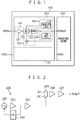
- FIG. 1 is a diagram illustrating a configuration example of an integrated circuit 100 according to a first embodiment.
- the integrated circuit 100 has a transmission circuit 101, a reception circuit 102, and a processing circuit 103.
- the processing circuit 103 is an internal circuit, and it generates internal data and outputs the parallel internal data TXIN to the transmission circuit 101.
- the transmission circuit 101 inputs the parallel internal data TXIN thereto, converts the parallel internal data TXIN to serial data, and transmits the serial data TXOUT.
- the reception circuit 102 has a front end 111, a logic unit 112, and a clock generating circuit 113.
- the front end 111 has a continuous time linear equalizer (CTLE) 131, a decision feedback equalizer (DFE) 132, and a demultiplexer 133.
- the logic unit 112 has an equalizer logic part 141, and a clock data recovery (CDR) logic part 142.
- the reception circuit 102 receives serial data RXIN.
- the CTLE 131 compensates a frequency characteristic of a transmission path with respect to the data RXIN.
- the DFE 132 performs, in synchronization with a clock signal generated by the clock generating circuit 113, equalization and binary determination on output data of the CTLE 131 based on an equalization coefficient output by the equalizer logic part 141.
- the demultiplexer 133 converts data output by the DFE 132 from serial data to parallel data.
- the equalizer logic part 141 outputs the equalization coefficient to the DFE 132 based on the parallel data output by the demultiplexer 133.
- the CDR logic part 142 controls a phase of the clock signal generated by the clock generating circuit 113 based on the parallel data output by the demultiplexer 133.
- the reception circuit 102 outputs the parallel data output by the demultiplexer 133 to the processing circuit 103 as reception data RXOUT.
- the processing circuit 103 processes the reception data RXOUT.
- FIG. 2 is a diagram illustrating a configuration example of a transmission circuit 200 to be a comparison example of the first embodiment.
- the transmission circuit 200 corresponds to the transmission circuit 101 in FIG. 1 .
- the transmission circuit 200 has a clock generating circuit 201, buffers 202, 204, 206, 207, a duty cycle corrector (DCC) 203, and a multiplexer 205.
- Data D1 and data D2 indicate parallel data corresponding to the data TXIN in FIG. 1 , but, data of 3-bit or more may also be employed.
- the clock generating circuit 201 generates a clock signal.
- the buffer 202 amplifies the clock signal generated by the clock generating circuit 201, and outputs the amplified clock signal.
- the duty cycle corrector 203 controls a phase of the clock signal generated by the clock generating circuit 201 so that a duty ratio of the clock signal output by the buffer 202 becomes 50%.
- the buffer 204 amplifies the clock signal output by the buffer 202, and outputs the amplified clock signal to the multiplexer 205.
- the multiplexer 205 converts the parallel data D1 and D2 to serial data in synchronization with the clock signal output by the buffer 204.
- the buffers 206 and 207 amplify the serial data, and transmit the amplified serial data TXOUT.
- the duty cycle corrector 203 corrects the duty ratio of the clock signal, the duty cycle distortion (DCD) sometimes occurs in the serial data TXOUT due to a mismatch of a threshold value of a transistor configuring the buffer 206, or insufficient band, and the like.
- DCD duty cycle distortion
- FIG. 3 is a diagram illustrating a configuration example of a transmission circuit 300 according to the first embodiment.
- the transmission circuit 300 corresponds to the transmission circuit 101 in FIG. 1 , and uses single-ended clock signal and data.
- the transmission circuit 300 has a clock generating circuit 301, a DCD adjusting circuit 302, a DCD detecting circuit 303, a DCD controlling circuit 304, buffers 305, 307, 308, and a multiplexer 306.
- the clock generating circuit 301 has a phase frequency comparator (PFC) 311, a charge pump (CP) 312, a low pass filter (LPF) 313, a voltage controlled oscillator (VCO) 314, and a frequency divider 315, and supplies a clock signal.
- the voltage controlled oscillator 314 generates a clock signal with a frequency according to an output voltage of the low pass filter 313.
- the frequency divider 315 divides the frequency of the clock signal generated by the voltage controlled oscillator 314, and outputs the frequency-divided clock signal to the phase frequency comparator 311.
- the phase frequency comparator 311 compares a phase frequency of the clock signal output by the frequency divider 315 and a phase frequency of a reference clock signal RCLK, and outputs an up signal or a down signal to the charge pump 312 according to a result of the comparison.
- the charge pump 312 increases the output voltage when the up signal is input thereto, and it lowers the output voltage when the down signal is input thereto.
- the low pass filter 313 performs low pass filtering on the output voltage of the charge pump 312, and outputs the low pass filtered voltage to the voltage controlled oscillator 314. Consequently, the voltage controlled oscillator 314 can generate a single-ended clock signal which is synchronized with the reference clock signal RCLK.
- the DCD adjusting circuit 302 has resistors 321 to 328, selectors 329, 330, capacitors 331, 332, a p-channel field effect transistor 333, and an n-channel field effect transistor 334.
- a node N1 is connected to an output node of the voltage controlled oscillator 314.
- the capacitor 331 is connected between a gate of the p-channel field effect transistor 333 and the node N1.
- the capacitor 332 is connected between a gate of the n-channel field effect transistor 334 and the node N1.
- the p-channel field effect transistor 333 has a source connected to a power supply potential node, and a drain connected to a node N2.
- the n-channel field effect transistor 334 has a drain connected to the node N2, and a source connected to a reference potential node (ground potential node).
- the plurality of resistors 321 to 324 are connected in series between the power supply potential node and the reference potential node, and output a plurality of voltages from interconnection points.
- the selector 329 applies, under the control of the DCD controlling circuit 304, one voltage among the plurality of voltages output by the resistors 321 to 324, to the gate of the p-channel field effect transistor 333.
- the plurality of resistors 325 to 328 are connected in series between the power supply potential node and the reference potential node, and output a plurality of voltages from interconnection points.
- the selector 330 applies, under the control of the DCD controlling circuit 304, one voltage among the plurality of voltages output by the resistors 325 to 328, to the gate of the n-channel field effect transistor 334.
- the p-channel field effect transistor 333 and the n-channel field effect transistor 334 configure an inverter, and output a clock signal as a result of inverting the clock signal at the node N1, from the node N2.
- the selectors 329 and 330 control an input common voltage of the inverter, to thereby control a duty ratio of the clock signal at the node N2 to adjust the DCD of the data TXOUT.
- the DCD adjusting circuit 302 can control the duty ratio of the clock signal at the node N2.
- the buffer 305 amplifies the clock signal at the node N2, and outputs the amplified clock signal to the multiplexer 306.
- the multiplexer 306 converts parallel data D1 and D2 to serial data in synchronization with the clock signal output by the buffer 305, and outputs the serial data.
- the multiplexer 306 converts the single-ended parallel data D1 and D2 to the single-ended serial data in synchronization with the single-ended clock signal. For example, the multiplexer 306 outputs the data D1 in a period in which the clock signal is at a high level, and it outputs the data D2 in a period in which the clock signal is at a low level. Specifically, the multiplexer 306 alternately outputs the data D1 and the data D2.
- the multiplexer 306 is a data generating circuit, and generates the serial data based on the clock signal.
- the buffer 307 amplifies the data output by the multiplexer 306, and outputs the amplified data.
- the buffer 308 is a buffer at a final stage of the transmission circuit 300, and it amplifies the data output by the buffer 307 and outputs the amplified data TXOUT.
- the transmission circuit 300 has a test mode and a normal mode.
- the test mode is a mode for adjusting the DCD of the data TXOUT.
- the normal mode is a mode for transmitting desired data TXOUT.
- the transmission circuit 300 adjusts the DCD of the data TXOUT in the test mode, and after that, it transmits the desired data TXOUT in the normal mode.
- the transmission circuit 300 is made to operate in the test mode when a power is supplied, for example, and inputs the data D1 fixed to "0" and the data D2 fixed to “1" thereto from the processing circuit 103.
- the data of "0" indicates a low level
- the data of "1” indicates a high level.
- the multiplexer 306 alternately outputs the data of "0” and the data of "1” in a manner such as "01010101 ⁇ ".
- the DCD detecting circuit 303 inputs output data of the buffer 307 and an intermediate potential vdd/2 thereto, and detects a duty cycle distortion (DCD) of the output data of the buffer 307.
- the output data of the buffer 307 at a high level is a potential vdd
- the output data of the buffer 307 at a low level is 0 V.
- the intermediate potential vdd/2 is a potential in the middle of the high-level potential vdd of the output data and the low-level potential 0 V of the output data.
- vdd is an operating power supply voltage of the integrated circuit 100, for example.
- the DCD is a distortion caused when a pulse width of data of "1" and a pulse width of data of "0" are different.
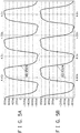
- FIG. 6A illustrates a waveform of data in which the DCD exists, in which a pulse width of data of "1” and a pulse width of data of "0" are different.
- FIG. 6B illustrates a waveform of data in which no DCD exists, in which a pulse width of data of "1” and a pulse width of data of "0" are the same.
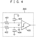
- FIG. 4 is a circuit diagram illustrating a configuration example of the DCD detecting circuit 303.
- the DCD detecting circuit 303 has resistors 401, 402, capacitors 403, 404, and a comparison circuit 405.
- the resistor 401 is connected between an output node of the buffer 307 in FIG. 3 and a node of an input potential V1 of the comparison circuit 405.
- the capacitor 403 is connected between the node of the input potential V1 of the comparison circuit 405 and a reference potential node.
- the resistor 401 and the capacitor 403 configure a low pass filter, and perform low pass filtering on an output potential (output signal) of the buffer 307 to output a time average value of the output potential of the buffer 307 as the input potential V1.
- the buffer 307 alternately outputs data at a low level and data at a high level. Therefore, when no DCD exists in the output potential of the buffer 307, the input potential V1 becomes the same potential as the intermediate potential vdd/2. Further, when the DCD exists in the output potential of the buffer 307, the input potential V1 becomes a potential different from the intermediate potential vdd/2.
- the resistor 402 is connected between a node of the intermediate potential vdd/2 in FIG. 3 and a node of an input potential V2 of the comparison circuit 405.
- the capacitor 404 is connected between the node of the input potential V2 of the comparison circuit 405 and a reference potential node.
- the resistor 402 and the capacitor 404 configure a low pass filter, and perform low pass filtering on the intermediate potential vdd/2 to output a time average value of the intermediate potential vdd/2 as the input potential V2.
- the input potential V2 becomes the same potential as the intermediate potential vdd/2.
- the comparison circuit 405 compares the input potential V1 and the input potential (threshold value) V2, and outputs a result of the comparison.
- the DCD controlling circuit 304 can determine that no DCD exists in the output data of the buffer 307 when the input potential V1 and the input potential V2 are the same, and determine that the DCD exists in the output data of the buffer 307 when the input potential V1 and the input potential V2 are different.
- the DCD controlling circuit 304 controls the selectors 329 and 330 so that the input potential V1 and the input potential V2 become the same. Consequently, it is possible to reduce the DCD that exists in the output data of the buffer 307 and the data TXOUT.
- the DCD adjusting circuit 302, the DCD detecting circuit 303, and the DCD controlling circuit 304 function as a duty ratio controlling circuit which detects the DCD of the data and controls the duty ratio of the clock signal based on the detection result.
- the DCD detecting circuit 303 inputs output data of the buffer 308 at the final stage (output data of an output terminal of the transmission circuit 300) TXOUT and an intermediate potential thereto, and detects the DCD of the output data TXOUT of the output terminal of the transmission circuit 300.
- the intermediate potential is a potential in the middle of the output data at a high level of the buffer 308 and the output data at a low level of the buffer 308. Consequently, it is possible to reduce the DCD of the output data TXOUT of the output terminal of the transmission circuit 300.
- an amplitude of the output data of the buffer 308 at the final stage is smaller than an amplitude of the output data of the buffer 307 which is previous to the buffer 308 by one stage, depending on an operating power supply voltage of a circuit (external system) to be a transmission destination of the output data of the transmission circuit 300.
- a circuit external system
- the amplitude of the output data of the buffer 308 is smaller than the amplitude of the output data of the buffer 307, there is a demerit that a detection accuracy of the DCD is lowered.
- the DCD detecting circuit 303 is connected to the output terminal of the transmission circuit 300, there is a demerit that the DCD detecting circuit 303 exerts an adverse effect on the external system such that impedance match is impaired.
- the DCD detecting circuit 303 inputs the input data of the buffer 308 at the final stage of the transmission circuit 300 (the output data of the buffer 307 which is previous to the buffer 308 by one stage) and the intermediate potential vdd/2 thereto, and detects the DCD of the input data of the buffer 308 at the final stage of the transmission circuit 300, as illustrated in FIG. 3 .
- the amplitude of the output data of the buffer 307 is larger than the amplitude of the output data of the buffer 308, it is possible to improve the detection accuracy of the DCD.
- the DCD detecting circuit 303 is not connected to the output terminal of the transmission circuit 300, it is possible to prevent the adverse effect exerted on the external system by the DCD detecting circuit 303.
- FIG. 5A is a diagram illustrating an example of waveform of a clock signal at the node N2 before performing the DCD adjustment.
- the selector 329 applies a potential in the middle of the power supply potential and the reference potential to the gate of the p-channel field effect transistor 333.
- the selector 330 applies a potential in the middle of the power supply potential and the reference potential to the gate of the n-channel field effect transistor 334.
- the node N2 outputs a clock signal illustrated in FIG. 5A .
- a duty ratio of the clock signal in FIG. 5A is about 50%.
- FIG. 6A is a diagram illustrating an example of waveform of output data of the buffer 307 before performing the DCD adjustment.
- the buffer 307 outputs data illustrated in FIG. 6A .
- This data is data in which data of "0" and data of "1" are alternately repeated. For example, this data at a high level is +1 V, and this data at a low level is - 1 V.
- the DCD detecting circuit 303 inputs the output potential of the buffer 307 and the intermediate potential 0 V thereto. In the data in FIG.
- a high-level period indicating the data of "1" is shorter than a low-level period indicating the data of "0", and thus there exists the DCD. Therefore, the input potential V1 in FIG. 4 becomes a negative potential.
- the input potential V2 becomes 0 V.
- the comparison circuit 405 outputs a signal indicating that the input potential V1 is lower than the input potential V2.
- the DCD controlling circuit 304 controls the selectors 329 and 330 based on the output signal of the comparison circuit 405, thereby performing the DCD adjustment.
- FIG. 5B is a diagram illustrating an example of waveform of a clock signal at the node N2 after performing the DCD adjustment.
- the selector 329 applies a potential lower than the potential in the middle of the power supply potential and the reference potential to the gate of the p-channel field effect transistor 333.
- the output potential of the selector 329 in FIG. 5B is lower than the output potential of the selector 329 in FIG. 5A .
- the selector 330 applies a potential higher than the potential in the middle of the power supply potential and the reference potential to the gate of the n-channel field effect transistor 334.
- the output potential of the selector 330 in FIG. 5B is higher than the output potential of the selector 330 in FIG. 5A .
- the node N2 outputs a clock signal illustrated in FIG. 5B .
- a duty ratio of the clock signal in FIG. 5B is about 54%.
- FIG. 6B is a diagram illustrating an example of waveform of output data of the buffer 307 after performing the DCD adjustment.
- the buffer 307 outputs data illustrated in FIG. 6B .
- a high-level period indicating the data of "1" is substantially the same as a low-level period indicating the data of "0", and thus there exists no DCD.
- the input potential V1 in FIG. 4 becomes substantially 0 V.
- the input potential V2 becomes 0 V.
- the input potential V1 is substantially the same as the input potential V2.
- the DCD controlling circuit 304 maintains the output potentials of the selectors 329 and 330 based on the output signal of the comparison circuit 405. Consequently, it is possible to reduce the DCD of the output data of the buffer 307 and the data TXOUT.
- FIG. 7 is a flow chart illustrating a control method of the test mode of the integrated circuit 100.
- the integrated circuit 100 performs preparation processing of the test mode.
- the processing circuit 103 fixes the data D1 to "0", and fixes the data D2 to "1".
- the multiplexer 306 outputs "010101 ⁇ ".
- the DCD controlling circuit 304 resets an adjustment code to an initial value, and outputs the adjustment code of the initial value to the selectors 329 and 330.
- the initial value of the adjustment code is a minimum value.
- step S702 the DCD controlling circuit 304 adds 1 to the adjustment code, and outputs the adjustment code after performing the addition to the selectors 329 and 330.
- the selector 329 applies a voltage according to the adjustment code to the gate of the p-channel field effect transistor 333.
- the selector 330 applies a voltage according to the adjustment code to the gate of the n-channel field effect transistor 334.
- step S703 the DCD controlling circuit 304 determines whether or not the input potential V1 is the same as the input potential V2 in FIG. 4 , based on an output signal of the DCD detecting circuit 303.
- the DCD controlling circuit 304 returns to step S702 to repeat the above-described processing.
- the input potential V1 becomes close to the input potential V2.
- the DCD controlling circuit 304 determines that the input potential V1 is the same as the input potential V2, it maintains the adjustment code, and terminates the processing of the test mode. Consequently, it is possible to reduce the DCD of the data TXOUT. After that, the integrated circuit 100 performs processing of the normal mode.
- the DCD detecting circuit 303 detects the DCD of the output data of the buffer 307 or 308.
- the DCD adjusting circuit 302 controls, under the control of the DCD controlling circuit 304, the duty ratio of the clock signal at the node N2 based on the detection result. This makes it possible to reduce the DCD of the data TXOUT. By reducing the DCD of the data TXOUT, the quality of the data TXOUT is improved, and the reception circuit can reduce a reproduction error of the received data TXOUT.
- FIG. 8 is a circuit diagram illustrating a configuration example of a DCD adjusting circuit 302 according to a second embodiment.
- An integrated circuit 100 according to the second embodiment is different from the integrated circuit 100 according to the first embodiment regarding the DCD adjusting circuit 302.
- a point at which the second embodiment is different from the first embodiment will be described.
- the DCD controlling circuit 302 has p-channel field effect transistors 333, 801, and n-channel field effect transistors 334, 802.
- the node N1 is connected to the voltage controlled oscillator 314 in FIG. 3 .
- the node N2 is connected to an input node of the buffer 305 in FIG. 3 .
- the p-channel field effect transistor 801 has a source connected to a power supply potential node, a gate connected to the DCD controlling circuit 304 in FIG. 3 , and a drain connected to a source of the p-channel field effect transistor 333.
- the p-channel field effect transistor 333 has a gate connected to the node N1, and a drain connected to the node N2.
- the n-channel field effect transistor 334 has a drain connected to the node N2, a gate connected to the node N1, and a source connected to a drain of the n-channel field effect transistor 802.
- the n-channel field effect transistor 802 has a gate connected to the DCD controlling circuit 304 in FIG. 3 , and a source connected to a reference potential node.
- the p-channel field effect transistor 801 functions as a resistor.
- the DCD controlling circuit 304 can change a resistance value of the p-channel field effect transistor 801 by controlling a gate voltage of the p-channel field effect transistor 801.
- the resistance value of the p-channel field effect transistor 801 and a parasitic capacitance connected to the node N2 configure a CR circuit, and can decide a rising speed (CR time constant) of a clock signal at the node N2.
- the DCD controlling circuit 304 can change the rising speed of the clock signal at the node N2 by controlling the resistance value of the p-channel field effect transistor 801.
- the n-channel field effect transistor 802 functions as a resistor.
- the DCD controlling circuit 304 can change a resistance value of the n-channel field effect transistor 802 by controlling a gate voltage of the n-channel field effect transistor 802.
- the resistance value of the n-channel field effect transistor 802 and a parasitic capacitance connected to the node N2 configure a CR circuit, and can decide a falling speed (CR time constant) of the clock signal at the node N2.
- the DCD controlling circuit 304 can change the falling speed of the clock signal at the node N2 by controlling the resistance value of the n-channel field effect transistor 802.
- the DCD controlling circuit 304 can change a duty ratio of the clock signal at the node N2 by controlling the rising speed and the falling speed of the clock signal at the node N2.
- the DCD controlling circuit 304 controls each of the resistance value of the p-channel field effect transistor 801 and the resistance value of the n-channel field effect transistor 802 to a standard value. Consequently, the duty ratio of the clock signal at the node N2 becomes about 50%, as illustrated in FIG. 5A . In that case, the buffer 307 outputs data in which the DCD exists, as illustrated in FIG. 6A .
- the DCD controlling circuit 304 makes the resistance value of the p-channel field effect transistor 801 to be smaller than the standard value, and makes the resistance value of the n-channel field effect transistor 802 to be larger than the standard value. Consequently, the rising speed of the clock signal at the node N2 becomes fast, and the falling speed of the clock signal at the node N2 becomes slow, resulting in that the duty ratio becomes larger than 50%, as illustrated in FIG. 5B . In that case, the buffer 307 can output data in which no DCD exists, as illustrated in FIG. 6B .
- the DCD controlling circuit 304 controls the rising speed and the falling speed of the clock signal at the node N2, based on the detection result obtained by the DCD detecting circuit 303. This makes it possible to reduce the DCD of the data TXOUT.
- FIG. 9 is a diagram illustrating a configuration example of a transmission circuit 900 according to a third embodiment.
- the transmission circuit 900 corresponds to the transmission circuit 101 in FIG. 1 , and uses differential clock signals and data.
- An integrated circuit 100 according to the third embodiment is different from the integrated circuit 100 according to the first embodiment regarding the transmission circuit 900.
- a point at which the third embodiment is different from the first embodiment will be described.
- the voltage controlled oscillator 314 outputs a first clock signal and a second clock signal which are mutually inverted.
- the first clock signal and the second clock signal are differential signals.
- a node N1a is a node of the first clock signal.
- a node N1b is a node of the second clock signal.
- a DCD adjusting circuit 302 has resistors 321a to 328a, 321b to 328b, selectors 329a, 330a, 329b, 330b, capacitors 331a, 332a, 331b, 332b, p-channel field effect transistors 333a, 333b, and n-channel field effect transistors 334a, 334b.
- the capacitor 331a is connected between a gate of the p-channel field effect transistor 333a and the node N1a.
- the capacitor 332a is connected between a gate of the n-channel field effect transistor 334a and the node N1a.
- the p-channel field effect transistor 333a has a source connected to a power supply potential node, and a drain connected to a node N2a.
- the n-channel field effect transistor 334a has a drain connected to the node N2a, and a source connected to a reference potential node.
- the capacitor 331b is connected between a gate of the p-channel field effect transistor 333b and the node N1b.
- the capacitor 332b is connected between a gate of the n-channel field effect transistor 334b and the node N1b.
- the p-channel field effect transistor 333b has a source connected to a power supply potential node, and a drain connected to a node N2b.
- the n-channel field effect transistor 334b has a drain connected to the node N2b, and a source connected to a reference potential node.
- the plurality of resistors 321a to 324a are connected in series between the power supply potential node and the reference potential node, and output a plurality of voltages from interconnection points.
- the selector 329a applies, under the control of the DCD controlling circuit 304, one voltage among the plurality of voltages output by the resistors 321a to 324a, to the gate of the p-channel field effect transistor 333a.
- the plurality of resistors 325a to 328a are connected in series between the power supply potential node and the reference potential node, and output a plurality of voltages from interconnection points.
- the selector 330a applies, under the control of the DCD controlling circuit 304, one voltage among the plurality of voltages output by the resistors 325a to 328a, to the gate of the n-channel field effect transistor 334a.
- the plurality of resistors 321b to 324b are connected in series between the power supply potential node and the reference potential node, and output a plurality of voltages from interconnection points.
- the selector 329b applies, under the control of the DCD controlling circuit 304, one voltage among the plurality of voltages output by the resistors 321b to 324b, to the gate of the p-channel field effect transistor 333b.
- the plurality of resistors 325b to 328b are connected in series between the power supply potential node and the reference potential node, and output a plurality of voltages from interconnection points.
- the selector 330b applies, under the control of the DCD controlling circuit 304, one voltage among the plurality of voltages output by the resistors 325b to 328b, to the gate of the n-channel field effect transistor 334b.
- the p-channel field effect transistor 333a and the n-channel field effect transistor 334a configure an inverter, invert the first clock signal at the node N1a and output the inverted clock signal to the node N2a.
- the p-channel field effect transistor 333b and the n-channel field effect transistor 334b configure an inverter, invert the second clock signal at the node N1b and output the inverted clock signal to the node N2b.
- the clock signal at the node N2a and the clock signal at the node N2b are mutually-inverted differential signals.
- the selectors 329a, 330a, 329b, and 330b control input common voltages of those inverters to adjust duty ratios of the clock signals at the nodes N2a and N2b, thereby adjusting the DCD of the data TXOUT.
- the buffer 305 is a differential buffer, amplifies the differential clock signals at the nodes N2a and N2b, and output the amplified differential clock signals to multiplexers 306a and 306b.
- the multiplexer 306a converts, in synchronization with the differential clock signals output by the buffer 305, parallel data D1 and D2 to serial data, and outputs the serial data.
- An inverter 901a outputs data as a result of inverting the data D1.
- An inverter 901b outputs data as a result of inverting the data D2.
- the multiplexer 306b converts, in synchronization with the differential clock signals output by the buffer 305, the parallel data output by the inverters 901a and 901b to serial data, and outputs the serial data.
- the serial data output by the multiplexer 306a and the serial data output by the multiplexer 306b are mutually-inverted differential data.
- the multiplexers 306a and 306b convert, in synchronization with the differential clock signals, the differential parallel data D1 and D2 to the differential serial data.
- the buffer 305 outputs differential clock signals formed of a third clock signal and a fourth clock signal.
- the multiplexer 306a outputs the data D1 in a period in which the third clock signal is at a high level, and outputs the data D2 in a period in which the fourth clock signal is at a high level. Specifically, the multiplexer 306a alternately outputs the data D1 and the data D2.
- the multiplexer 306b outputs the output data of the inverter 901a in a period in which the fourth clock signal is at a high level, and outputs the output data of the inverter 901b in a period in which the third clock signal is at a high level. Specifically, the multiplexer 306b alternately outputs the output data of the inverter 901a and the output data of the inverter 901b.
- a buffer 307a amplifies the data output by the multiplexer 306a, and outputs the amplified data.
- a buffer 308a is a buffer at a final stage of the transmission circuit 900, amplifies the data output by the buffer 307a, and outputs the amplified data TXOUTa.
- a buffer 307b amplifies the data output by the multiplexer 306b, and outputs the amplified data.
- a buffer 308b is a buffer at a final stage of the transmission circuit 900, amplifies the data output by the buffer 307b, and outputs the amplified data TXOUTb.
- the data TXOUTa and the data TXOUTb are mutually-inverted differential data.
- the transmission circuit 900 transmits the data TXOUTa and TXOUTb.
- the transmission circuit 900 inputs the data D1 fixed to "0" and the data D2 fixed to “1" thereto from the processing circuit 103.
- the multiplexer 306a outputs data in which the data of "0” and the data of "1” are alternately repeated in a manner such as “01010101 ⁇ ”.
- the multiplexer 306b outputs data in which the data of "1” and the data of "0” are alternately repeated in a manner such as "101010 ⁇ ".
- the DCD detecting circuit 303 inputs the output data of the buffer 307a and the output data of the buffer 307b thereto, and detects a duty cycle distortion (DCD) of the output data of the buffers 307a and 307b.
- the DCD detecting circuit 303 has a configuration illustrated in FIG. 4 .
- the resistor 401 is connected to an output node of the buffer 307a.
- the resistor 401 and the capacitor 403 generate an input potential V1 obtained by performing low pass filtering on an output potential (output signal) of the buffer 307a.
- the resistor 402 is connected to an output node of the buffer 307b.
- the resistor 402 and the capacitor 404 generate an input potential V2 obtained by performing low pass filtering on an output potential (output signal) of the buffer 307b.
- the buffer 307a alternately outputs data at a low level and data at a high level. Therefore, when no DCD exists in the output potential of the buffer 307a, the input potential V1 becomes the same potential as the intermediate potential vdd/2. Further, when the DCD exists in the output potential of the buffer 307a, the input potential V1 becomes a potential different from the intermediate potential vdd/2.
- the buffer 307b alternately outputs data at a high level and data at a low level. Therefore, when no DCD exists in the output potential of the buffer 307b, the input potential V2 becomes the same potential as the intermediate potential vdd/2. Further, when the DCD exists in the output potential of the buffer 307b, the input potential V2 becomes a potential different from the intermediate potential vdd/2.
- the comparison circuit 405 compares the input potential V1 and the input potential V2, and outputs a result of the comparison.
- the DCD controlling circuit 304 determines that no DCD exists in the output data of the buffers 307a and 307b when the input potential V1 and the input potential V2 are the same. Further, the DCD controlling circuit 304 determines that the DCD exists in the output data of the buffers 307a and 307b when the input potential V1 and the input potential V2 are different. The DCD controlling circuit 304 controls the selectors 329a, 330a, 329b, and 330b so that the input potential V1 and the input potential V2 become the same. Consequently, it is possible to reduce the DCD that exists in the data TXOUTa and TXOUTb.
- the DCD detecting circuit 303 inputs the output data of the buffers 308a and 308b at the final stage (output data of output terminals of the transmission circuit 900) TXOUTa and TXOUTb thereto, and detects the DCD of the output data TXOUTa and TXOUTb of the output terminals of the transmission circuit 900, similarly to the first embodiment.
- the DCD controlling circuit 302 has a configuration similar to the configuration in FIG. 8 , and controls a rising speed and a falling speed of the clock signals at the nodes N2a and N2b, similarly to the second embodiment.
- the DCD detecting circuit 303 detects the DCD of the differential data.
- the DCD adjusting circuit 302 controls, under the control of the DCD controlling circuit 304, the duty ratio of the differential clock signals at the nodes N2a and N2b based on the detection result. This makes it possible to reduce the DCD of the differential data TXOUTa and TXOUTb. By reducing the DCD of the data TXOUTa and TXOUTb, the quality of the data TXOUTa and TXOUTb is improved, and the reception circuit can reduce a reproduction error of the received data TXOUTa and TXOUTb.
Landscapes
- Physics & Mathematics (AREA)
- Nonlinear Science (AREA)
- Logic Circuits (AREA)
- Pulse Circuits (AREA)
- Dc Digital Transmission (AREA)
- Manipulation Of Pulses (AREA)
Abstract
Description
- The embodiments discussed herein are directed to a transmission circuit and an integrated circuit.
- There is known a duty ratio correcting circuit having an input buffer for clock to which a first clock signal is input, and an input buffer for data to which a first data signal is input (refer to Patent Document 1). A duty adjusting circuit for clock adjusts, based on a correction signal, a duty ratio of a second clock signal output from the input buffer for clock, to thereby generate a third clock signal. A duty adjusting circuit for data adjusts, based on the correction signal, a duty ratio of a second data signal output from the input buffer for data, to thereby generate a third data signal. A duty comparison circuit generates the correction signal based on the third clock signal.
- Further, there is known a clock/data recovery circuit having a data duty correcting circuit for outputting correction data obtained by correcting the duty of input data according to the level of a correction signal (refer to Patent Document 2). A clock recovery circuit generates a recovered clock synchronized with the edge timing of the correction data. A data identifying circuit identifies the correction data by the recovered clock. A data duty detecting circuit detects the duty of the correction data by the recovered clock and outputs the correction signal indicating a duty correction amount to the data duty correcting circuit.
- Patent Document 1: Japanese Laid-open Patent Publication No.
2010-206348 - Patent Document 2: International Publication Pamphlet No.
WO 2008/111241 - A duty cycle distortion (DCD) is a distortion caused when a pulse width of data of 1 and a pulse width of data of 0 are different. When data is generated based on a clock signal, even if a duty ratio of the clock signal is corrected to 50%, a duty cycle distortion sometimes occurs in the data.
- A transmission circuit comprising: a data generating circuit configured to generate data based on a clock signal; a clock generating circuit configured to supply the clock signal to the data generating circuit; and a duty ratio controlling circuit configured to detect a duty cycle distortion of the data output from the data generating circuit, and control a duty ratio of the clock signal based on a result of the detection.
- An integrated circuit, comprising: a processing circuit configured to generate internal data; and a transmission circuit configured to input the internal data thereto, wherein the transmission circuit comprises: a data generating circuit configured to generate data based on a clock signal; a clock generating circuit configured to supply the clock signal to the data generating circuit; and a duty ratio controlling circuit configured to detect a duty cycle distortion of the data output from the data generating circuit, and control a duty ratio of the clock signal based on a result of the detection.
- Advantageously, the transmission circuit and the integrated circuit are capable of reducing a duty cycle distortion.
-
-
FIG. 1 is a diagram illustrating a configuration example of an integrated circuit according to a first embodiment; -
FIG. 2 is a diagram illustrating a configuration example of a transmission circuit according to a basic technique; -
FIG. 3 is a diagram illustrating a configuration example of a transmission circuit according to the first embodiment; -
FIG. 4 is a circuit diagram illustrating a configuration example of a DCD detecting circuit; -
FIG. 5A is a diagram illustrating an example of waveform of a clock signal before performing DCD adjustment, andFIG. 5B is a diagram illustrating an example of waveform of a clock signal after performing the DCD adjustment; -
FIG. 6A is a diagram illustrating an example of waveform of data before performing the DCD adjustment, andFIG. 6B is a diagram illustrating an example of waveform of data after performing the DCD adjustment; -
FIG. 7 is a flow chart illustrating a control method of a test mode of the integrated circuit; -
FIG. 8 is a circuit diagram illustrating a configuration example of a DCD adjusting circuit according to a second embodiment; and -
FIG. 9 is a diagram illustrating a configuration example of a transmission circuit according to a third embodiment. -
FIG. 1 is a diagram illustrating a configuration example of an integratedcircuit 100 according to a first embodiment. Theintegrated circuit 100 has a transmission circuit 101, areception circuit 102, and aprocessing circuit 103. Theprocessing circuit 103 is an internal circuit, and it generates internal data and outputs the parallel internal data TXIN to the transmission circuit 101. The transmission circuit 101 inputs the parallel internal data TXIN thereto, converts the parallel internal data TXIN to serial data, and transmits the serial data TXOUT. - The
reception circuit 102 has afront end 111, alogic unit 112, and aclock generating circuit 113. Thefront end 111 has a continuous time linear equalizer (CTLE) 131, a decision feedback equalizer (DFE) 132, and ademultiplexer 133. Thelogic unit 112 has anequalizer logic part 141, and a clock data recovery (CDR)logic part 142. - The
reception circuit 102 receives serial data RXIN. TheCTLE 131 compensates a frequency characteristic of a transmission path with respect to the data RXIN. The DFE 132 performs, in synchronization with a clock signal generated by theclock generating circuit 113, equalization and binary determination on output data of theCTLE 131 based on an equalization coefficient output by theequalizer logic part 141. Thedemultiplexer 133 converts data output by the DFE 132 from serial data to parallel data. Theequalizer logic part 141 outputs the equalization coefficient to the DFE 132 based on the parallel data output by thedemultiplexer 133. TheCDR logic part 142 controls a phase of the clock signal generated by theclock generating circuit 113 based on the parallel data output by thedemultiplexer 133. Thereception circuit 102 outputs the parallel data output by thedemultiplexer 133 to theprocessing circuit 103 as reception data RXOUT. Theprocessing circuit 103 processes the reception data RXOUT. -
FIG. 2 is a diagram illustrating a configuration example of atransmission circuit 200 to be a comparison example of the first embodiment. Thetransmission circuit 200 corresponds to the transmission circuit 101 inFIG. 1 . Thetransmission circuit 200 has aclock generating circuit 201,buffers multiplexer 205. Data D1 and data D2 indicate parallel data corresponding to the data TXIN inFIG. 1 , but, data of 3-bit or more may also be employed. - The clock generating
circuit 201 generates a clock signal. Thebuffer 202 amplifies the clock signal generated by theclock generating circuit 201, and outputs the amplified clock signal. Theduty cycle corrector 203 controls a phase of the clock signal generated by theclock generating circuit 201 so that a duty ratio of the clock signal output by thebuffer 202 becomes 50%. Thebuffer 204 amplifies the clock signal output by thebuffer 202, and outputs the amplified clock signal to themultiplexer 205. Themultiplexer 205 converts the parallel data D1 and D2 to serial data in synchronization with the clock signal output by thebuffer 204. Thebuffers - Even if the
duty cycle corrector 203 corrects the duty ratio of the clock signal, the duty cycle distortion (DCD) sometimes occurs in the serial data TXOUT due to a mismatch of a threshold value of a transistor configuring thebuffer 206, or insufficient band, and the like. Hereinafter, a transmission circuit capable of reducing the duty cycle distortion of the serial data TXOUT will be explained while referring toFIG. 3 . -
FIG. 3 is a diagram illustrating a configuration example of atransmission circuit 300 according to the first embodiment. Thetransmission circuit 300 corresponds to the transmission circuit 101 inFIG. 1 , and uses single-ended clock signal and data. Thetransmission circuit 300 has aclock generating circuit 301, a DCD adjustingcircuit 302, aDCD detecting circuit 303, aDCD controlling circuit 304,buffers multiplexer 306. - The
clock generating circuit 301 has a phase frequency comparator (PFC) 311, a charge pump (CP) 312, a low pass filter (LPF) 313, a voltage controlled oscillator (VCO) 314, and afrequency divider 315, and supplies a clock signal. The voltage controlledoscillator 314 generates a clock signal with a frequency according to an output voltage of thelow pass filter 313. Thefrequency divider 315 divides the frequency of the clock signal generated by the voltage controlledoscillator 314, and outputs the frequency-divided clock signal to thephase frequency comparator 311. Thephase frequency comparator 311 compares a phase frequency of the clock signal output by thefrequency divider 315 and a phase frequency of a reference clock signal RCLK, and outputs an up signal or a down signal to thecharge pump 312 according to a result of the comparison. Thecharge pump 312 increases the output voltage when the up signal is input thereto, and it lowers the output voltage when the down signal is input thereto. Thelow pass filter 313 performs low pass filtering on the output voltage of thecharge pump 312, and outputs the low pass filtered voltage to the voltage controlledoscillator 314. Consequently, the voltage controlledoscillator 314 can generate a single-ended clock signal which is synchronized with the reference clock signal RCLK. - The
DCD adjusting circuit 302 hasresistors 321 to 328,selectors capacitors field effect transistor 333, and an n-channelfield effect transistor 334. A node N1 is connected to an output node of the voltage controlledoscillator 314. Thecapacitor 331 is connected between a gate of the p-channelfield effect transistor 333 and the node N1. Thecapacitor 332 is connected between a gate of the n-channelfield effect transistor 334 and the node N1. The p-channelfield effect transistor 333 has a source connected to a power supply potential node, and a drain connected to a node N2. The n-channelfield effect transistor 334 has a drain connected to the node N2, and a source connected to a reference potential node (ground potential node). - The plurality of
resistors 321 to 324 are connected in series between the power supply potential node and the reference potential node, and output a plurality of voltages from interconnection points. Theselector 329 applies, under the control of theDCD controlling circuit 304, one voltage among the plurality of voltages output by theresistors 321 to 324, to the gate of the p-channelfield effect transistor 333. - The plurality of
resistors 325 to 328 are connected in series between the power supply potential node and the reference potential node, and output a plurality of voltages from interconnection points. Theselector 330 applies, under the control of theDCD controlling circuit 304, one voltage among the plurality of voltages output by theresistors 325 to 328, to the gate of the n-channelfield effect transistor 334. - The p-channel
field effect transistor 333 and the n-channelfield effect transistor 334 configure an inverter, and output a clock signal as a result of inverting the clock signal at the node N1, from the node N2. Theselectors DCD adjusting circuit 302 can control the duty ratio of the clock signal at the node N2. - The
buffer 305 amplifies the clock signal at the node N2, and outputs the amplified clock signal to themultiplexer 306. Themultiplexer 306 converts parallel data D1 and D2 to serial data in synchronization with the clock signal output by thebuffer 305, and outputs the serial data. Themultiplexer 306 converts the single-ended parallel data D1 and D2 to the single-ended serial data in synchronization with the single-ended clock signal. For example, themultiplexer 306 outputs the data D1 in a period in which the clock signal is at a high level, and it outputs the data D2 in a period in which the clock signal is at a low level. Specifically, themultiplexer 306 alternately outputs the data D1 and the data D2. Themultiplexer 306 is a data generating circuit, and generates the serial data based on the clock signal. - The
buffer 307 amplifies the data output by themultiplexer 306, and outputs the amplified data. Thebuffer 308 is a buffer at a final stage of thetransmission circuit 300, and it amplifies the data output by thebuffer 307 and outputs the amplified data TXOUT. - The
transmission circuit 300 has a test mode and a normal mode. The test mode is a mode for adjusting the DCD of the data TXOUT. The normal mode is a mode for transmitting desired data TXOUT. Thetransmission circuit 300 adjusts the DCD of the data TXOUT in the test mode, and after that, it transmits the desired data TXOUT in the normal mode. - First, the
transmission circuit 300 is made to operate in the test mode when a power is supplied, for example, and inputs the data D1 fixed to "0" and the data D2 fixed to "1" thereto from theprocessing circuit 103. For example, the data of "0" indicates a low level, and the data of "1" indicates a high level. Themultiplexer 306 alternately outputs the data of "0" and the data of "1" in a manner such as "01010101···". - The
DCD detecting circuit 303 inputs output data of thebuffer 307 and an intermediate potential vdd/2 thereto, and detects a duty cycle distortion (DCD) of the output data of thebuffer 307. The output data of thebuffer 307 at a high level is a potential vdd, and the output data of thebuffer 307 at a low level is 0 V. The intermediate potential vdd/2 is a potential in the middle of the high-level potential vdd of the output data and the low-level potential 0 V of the output data. Here, vdd is an operating power supply voltage of theintegrated circuit 100, for example. - The DCD is a distortion caused when a pulse width of data of "1" and a pulse width of data of "0" are different. For example,
FIG. 6A illustrates a waveform of data in which the DCD exists, in which a pulse width of data of "1" and a pulse width of data of "0" are different.FIG. 6B illustrates a waveform of data in which no DCD exists, in which a pulse width of data of "1" and a pulse width of data of "0" are the same. -
FIG. 4 is a circuit diagram illustrating a configuration example of theDCD detecting circuit 303. TheDCD detecting circuit 303 hasresistors capacitors comparison circuit 405. Theresistor 401 is connected between an output node of thebuffer 307 inFIG. 3 and a node of an input potential V1 of thecomparison circuit 405. Thecapacitor 403 is connected between the node of the input potential V1 of thecomparison circuit 405 and a reference potential node. Theresistor 401 and thecapacitor 403 configure a low pass filter, and perform low pass filtering on an output potential (output signal) of thebuffer 307 to output a time average value of the output potential of thebuffer 307 as the input potential V1. In the test mode, thebuffer 307 alternately outputs data at a low level and data at a high level. Therefore, when no DCD exists in the output potential of thebuffer 307, the input potential V1 becomes the same potential as the intermediate potential vdd/2. Further, when the DCD exists in the output potential of thebuffer 307, the input potential V1 becomes a potential different from the intermediate potential vdd/2. - The
resistor 402 is connected between a node of the intermediate potential vdd/2 inFIG. 3 and a node of an input potential V2 of thecomparison circuit 405. Thecapacitor 404 is connected between the node of the input potential V2 of thecomparison circuit 405 and a reference potential node. Theresistor 402 and thecapacitor 404 configure a low pass filter, and perform low pass filtering on the intermediate potential vdd/2 to output a time average value of the intermediate potential vdd/2 as the input potential V2. The input potential V2 becomes the same potential as the intermediate potential vdd/2. Thecomparison circuit 405 compares the input potential V1 and the input potential (threshold value) V2, and outputs a result of the comparison. - In
FIG. 3 , theDCD controlling circuit 304 can determine that no DCD exists in the output data of thebuffer 307 when the input potential V1 and the input potential V2 are the same, and determine that the DCD exists in the output data of thebuffer 307 when the input potential V1 and the input potential V2 are different. The DCDcontrolling circuit 304 controls theselectors buffer 307 and the data TXOUT. - As described above, the
DCD adjusting circuit 302, theDCD detecting circuit 303, and theDCD controlling circuit 304 function as a duty ratio controlling circuit which detects the DCD of the data and controls the duty ratio of the clock signal based on the detection result. - Note that it is possible that the
DCD detecting circuit 303 inputs output data of thebuffer 308 at the final stage (output data of an output terminal of the transmission circuit 300) TXOUT and an intermediate potential thereto, and detects the DCD of the output data TXOUT of the output terminal of thetransmission circuit 300. The intermediate potential is a potential in the middle of the output data at a high level of thebuffer 308 and the output data at a low level of thebuffer 308. Consequently, it is possible to reduce the DCD of the output data TXOUT of the output terminal of thetransmission circuit 300. However, there is a case where an amplitude of the output data of thebuffer 308 at the final stage is smaller than an amplitude of the output data of thebuffer 307 which is previous to thebuffer 308 by one stage, depending on an operating power supply voltage of a circuit (external system) to be a transmission destination of the output data of thetransmission circuit 300. In this case, since the amplitude of the output data of thebuffer 308 is smaller than the amplitude of the output data of thebuffer 307, there is a demerit that a detection accuracy of the DCD is lowered. Further, since theDCD detecting circuit 303 is connected to the output terminal of thetransmission circuit 300, there is a demerit that theDCD detecting circuit 303 exerts an adverse effect on the external system such that impedance match is impaired. - In order to eliminate the above-described demerits, it is preferable that the
DCD detecting circuit 303 inputs the input data of thebuffer 308 at the final stage of the transmission circuit 300 (the output data of thebuffer 307 which is previous to thebuffer 308 by one stage) and the intermediate potential vdd/2 thereto, and detects the DCD of the input data of thebuffer 308 at the final stage of thetransmission circuit 300, as illustrated inFIG. 3 . In this case, since the amplitude of the output data of thebuffer 307 is larger than the amplitude of the output data of thebuffer 308, it is possible to improve the detection accuracy of the DCD. Further, since theDCD detecting circuit 303 is not connected to the output terminal of thetransmission circuit 300, it is possible to prevent the adverse effect exerted on the external system by theDCD detecting circuit 303. -
FIG. 5A is a diagram illustrating an example of waveform of a clock signal at the node N2 before performing the DCD adjustment. Theselector 329 applies a potential in the middle of the power supply potential and the reference potential to the gate of the p-channelfield effect transistor 333. Theselector 330 applies a potential in the middle of the power supply potential and the reference potential to the gate of the n-channelfield effect transistor 334. In this case, the node N2 outputs a clock signal illustrated inFIG. 5A . A duty ratio of the clock signal inFIG. 5A is about 50%. -
FIG. 6A is a diagram illustrating an example of waveform of output data of thebuffer 307 before performing the DCD adjustment. When the node N2 outputs the clock signal illustrated inFIG. 5A , thebuffer 307 outputs data illustrated inFIG. 6A . This data is data in which data of "0" and data of "1" are alternately repeated. For example, this data at a high level is +1 V, and this data at a low level is - 1 V. In this case, theDCD detecting circuit 303 inputs the output potential of thebuffer 307 and the intermediate potential 0 V thereto. In the data inFIG. 6A , a high-level period indicating the data of "1" is shorter than a low-level period indicating the data of "0", and thus there exists the DCD. Therefore, the input potential V1 inFIG. 4 becomes a negative potential. The input potential V2 becomes 0 V. Thecomparison circuit 405 outputs a signal indicating that the input potential V1 is lower than the input potential V2. The DCDcontrolling circuit 304 controls theselectors comparison circuit 405, thereby performing the DCD adjustment. -
FIG. 5B is a diagram illustrating an example of waveform of a clock signal at the node N2 after performing the DCD adjustment. Theselector 329 applies a potential lower than the potential in the middle of the power supply potential and the reference potential to the gate of the p-channelfield effect transistor 333. The output potential of theselector 329 inFIG. 5B is lower than the output potential of theselector 329 inFIG. 5A . Further, theselector 330 applies a potential higher than the potential in the middle of the power supply potential and the reference potential to the gate of the n-channelfield effect transistor 334. The output potential of theselector 330 inFIG. 5B is higher than the output potential of theselector 330 inFIG. 5A . In this case, the node N2 outputs a clock signal illustrated inFIG. 5B . A duty ratio of the clock signal inFIG. 5B is about 54%. -
FIG. 6B is a diagram illustrating an example of waveform of output data of thebuffer 307 after performing the DCD adjustment. When the node N2 outputs the clock signal illustrated inFIG. 5B , thebuffer 307 outputs data illustrated inFIG. 6B . Regarding the data inFIG. 6B , a high-level period indicating the data of "1" is substantially the same as a low-level period indicating the data of "0", and thus there exists no DCD. The input potential V1 inFIG. 4 becomes substantially 0 V. The input potential V2 becomes 0 V. The input potential V1 is substantially the same as the input potential V2. The DCDcontrolling circuit 304 maintains the output potentials of theselectors comparison circuit 405. Consequently, it is possible to reduce the DCD of the output data of thebuffer 307 and the data TXOUT. -
FIG. 7 is a flow chart illustrating a control method of the test mode of theintegrated circuit 100. In step S701, theintegrated circuit 100 performs preparation processing of the test mode. Theprocessing circuit 103 fixes the data D1 to "0", and fixes the data D2 to "1". Themultiplexer 306 outputs "010101···". The DCDcontrolling circuit 304 resets an adjustment code to an initial value, and outputs the adjustment code of the initial value to theselectors - Next, in step S702, the
DCD controlling circuit 304 adds 1 to the adjustment code, and outputs the adjustment code after performing the addition to theselectors selector 329 applies a voltage according to the adjustment code to the gate of the p-channelfield effect transistor 333. Theselector 330 applies a voltage according to the adjustment code to the gate of the n-channelfield effect transistor 334. - Next, in step S703, the
DCD controlling circuit 304 determines whether or not the input potential V1 is the same as the input potential V2 inFIG. 4 , based on an output signal of theDCD detecting circuit 303. When the input potential V1 is not the same as the input potential V2, theDCD controlling circuit 304 returns to step S702 to repeat the above-described processing. In accordance with the increment of the adjustment code, the input potential V1 becomes close to the input potential V2. When theDCD controlling circuit 304 determines that the input potential V1 is the same as the input potential V2, it maintains the adjustment code, and terminates the processing of the test mode. Consequently, it is possible to reduce the DCD of the data TXOUT. After that, theintegrated circuit 100 performs processing of the normal mode. - As described above, even when the duty ratio of the clock signal at the node N2 is 50%, the DCD sometimes exists in the data TXOUT due to a mismatch of a threshold value of a transistor configuring the
buffer 307, and the like. According to the present embodiment, theDCD detecting circuit 303 detects the DCD of the output data of thebuffer DCD adjusting circuit 302 controls, under the control of theDCD controlling circuit 304, the duty ratio of the clock signal at the node N2 based on the detection result. This makes it possible to reduce the DCD of the data TXOUT. By reducing the DCD of the data TXOUT, the quality of the data TXOUT is improved, and the reception circuit can reduce a reproduction error of the received data TXOUT. -
FIG. 8 is a circuit diagram illustrating a configuration example of aDCD adjusting circuit 302 according to a second embodiment. Anintegrated circuit 100 according to the second embodiment is different from theintegrated circuit 100 according to the first embodiment regarding theDCD adjusting circuit 302. Hereinafter, a point at which the second embodiment is different from the first embodiment will be described. - The DCD
controlling circuit 302 has p-channelfield effect transistors field effect transistors oscillator 314 inFIG. 3 . The node N2 is connected to an input node of thebuffer 305 inFIG. 3 . - The p-channel
field effect transistor 801 has a source connected to a power supply potential node, a gate connected to theDCD controlling circuit 304 inFIG. 3 , and a drain connected to a source of the p-channelfield effect transistor 333. The p-channelfield effect transistor 333 has a gate connected to the node N1, and a drain connected to the node N2. The n-channelfield effect transistor 334 has a drain connected to the node N2, a gate connected to the node N1, and a source connected to a drain of the n-channelfield effect transistor 802. The n-channelfield effect transistor 802 has a gate connected to theDCD controlling circuit 304 inFIG. 3 , and a source connected to a reference potential node. - The p-channel
field effect transistor 801 functions as a resistor. The DCDcontrolling circuit 304 can change a resistance value of the p-channelfield effect transistor 801 by controlling a gate voltage of the p-channelfield effect transistor 801. The resistance value of the p-channelfield effect transistor 801 and a parasitic capacitance connected to the node N2 configure a CR circuit, and can decide a rising speed (CR time constant) of a clock signal at the node N2. The DCDcontrolling circuit 304 can change the rising speed of the clock signal at the node N2 by controlling the resistance value of the p-channelfield effect transistor 801. - In a similar manner, the n-channel
field effect transistor 802 functions as a resistor. The DCDcontrolling circuit 304 can change a resistance value of the n-channelfield effect transistor 802 by controlling a gate voltage of the n-channelfield effect transistor 802. The resistance value of the n-channelfield effect transistor 802 and a parasitic capacitance connected to the node N2 configure a CR circuit, and can decide a falling speed (CR time constant) of the clock signal at the node N2. The DCDcontrolling circuit 304 can change the falling speed of the clock signal at the node N2 by controlling the resistance value of the n-channelfield effect transistor 802. - The DCD
controlling circuit 304 can change a duty ratio of the clock signal at the node N2 by controlling the rising speed and the falling speed of the clock signal at the node N2. - For example, the
DCD controlling circuit 304 controls each of the resistance value of the p-channelfield effect transistor 801 and the resistance value of the n-channelfield effect transistor 802 to a standard value. Consequently, the duty ratio of the clock signal at the node N2 becomes about 50%, as illustrated inFIG. 5A . In that case, thebuffer 307 outputs data in which the DCD exists, as illustrated inFIG. 6A . - After that, the
DCD controlling circuit 304 makes the resistance value of the p-channelfield effect transistor 801 to be smaller than the standard value, and makes the resistance value of the n-channelfield effect transistor 802 to be larger than the standard value. Consequently, the rising speed of the clock signal at the node N2 becomes fast, and the falling speed of the clock signal at the node N2 becomes slow, resulting in that the duty ratio becomes larger than 50%, as illustrated inFIG. 5B . In that case, thebuffer 307 can output data in which no DCD exists, as illustrated inFIG. 6B . - As described above, the
DCD controlling circuit 304 controls the rising speed and the falling speed of the clock signal at the node N2, based on the detection result obtained by theDCD detecting circuit 303. This makes it possible to reduce the DCD of the data TXOUT. -
FIG. 9 is a diagram illustrating a configuration example of atransmission circuit 900 according to a third embodiment. Thetransmission circuit 900 corresponds to the transmission circuit 101 inFIG. 1 , and uses differential clock signals and data. Anintegrated circuit 100 according to the third embodiment is different from theintegrated circuit 100 according to the first embodiment regarding thetransmission circuit 900. Hereinafter, a point at which the third embodiment is different from the first embodiment will be described. - In the
clock generating circuit 301, the voltage controlledoscillator 314 outputs a first clock signal and a second clock signal which are mutually inverted. The first clock signal and the second clock signal are differential signals. A node N1a is a node of the first clock signal. A node N1b is a node of the second clock signal. - A
DCD adjusting circuit 302 hasresistors 321a to 328a, 321b to 328b,selectors capacitors field effect transistors field effect transistors - The
capacitor 331a is connected between a gate of the p-channelfield effect transistor 333a and the node N1a. Thecapacitor 332a is connected between a gate of the n-channelfield effect transistor 334a and the node N1a. The p-channelfield effect transistor 333a has a source connected to a power supply potential node, and a drain connected to a node N2a. The n-channelfield effect transistor 334a has a drain connected to the node N2a, and a source connected to a reference potential node. - The capacitor 331b is connected between a gate of the p-channel
field effect transistor 333b and the node N1b. Thecapacitor 332b is connected between a gate of the n-channelfield effect transistor 334b and the node N1b. The p-channelfield effect transistor 333b has a source connected to a power supply potential node, and a drain connected to a node N2b. The n-channelfield effect transistor 334b has a drain connected to the node N2b, and a source connected to a reference potential node. - The plurality of
resistors 321a to 324a are connected in series between the power supply potential node and the reference potential node, and output a plurality of voltages from interconnection points. Theselector 329a applies, under the control of theDCD controlling circuit 304, one voltage among the plurality of voltages output by theresistors 321a to 324a, to the gate of the p-channelfield effect transistor 333a. - The plurality of
resistors 325a to 328a are connected in series between the power supply potential node and the reference potential node, and output a plurality of voltages from interconnection points. Theselector 330a applies, under the control of theDCD controlling circuit 304, one voltage among the plurality of voltages output by theresistors 325a to 328a, to the gate of the n-channelfield effect transistor 334a. - The plurality of
resistors 321b to 324b are connected in series between the power supply potential node and the reference potential node, and output a plurality of voltages from interconnection points. Theselector 329b applies, under the control of theDCD controlling circuit 304, one voltage among the plurality of voltages output by theresistors 321b to 324b, to the gate of the p-channelfield effect transistor 333b. - The plurality of
resistors 325b to 328b are connected in series between the power supply potential node and the reference potential node, and output a plurality of voltages from interconnection points. Theselector 330b applies, under the control of theDCD controlling circuit 304, one voltage among the plurality of voltages output by theresistors 325b to 328b, to the gate of the n-channelfield effect transistor 334b. - The p-channel
field effect transistor 333a and the n-channelfield effect transistor 334a configure an inverter, invert the first clock signal at the node N1a and output the inverted clock signal to the node N2a. The p-channelfield effect transistor 333b and the n-channelfield effect transistor 334b configure an inverter, invert the second clock signal at the node N1b and output the inverted clock signal to the node N2b. The clock signal at the node N2a and the clock signal at the node N2b are mutually-inverted differential signals. Theselectors - The
buffer 305 is a differential buffer, amplifies the differential clock signals at the nodes N2a and N2b, and output the amplified differential clock signals tomultiplexers multiplexer 306a converts, in synchronization with the differential clock signals output by thebuffer 305, parallel data D1 and D2 to serial data, and outputs the serial data. Aninverter 901a outputs data as a result of inverting the data D1. Aninverter 901b outputs data as a result of inverting the data D2. Themultiplexer 306b converts, in synchronization with the differential clock signals output by thebuffer 305, the parallel data output by theinverters multiplexer 306a and the serial data output by themultiplexer 306b are mutually-inverted differential data. Themultiplexers - For example, the
buffer 305 outputs differential clock signals formed of a third clock signal and a fourth clock signal. Themultiplexer 306a outputs the data D1 in a period in which the third clock signal is at a high level, and outputs the data D2 in a period in which the fourth clock signal is at a high level. Specifically, themultiplexer 306a alternately outputs the data D1 and the data D2. - The
multiplexer 306b outputs the output data of theinverter 901a in a period in which the fourth clock signal is at a high level, and outputs the output data of theinverter 901b in a period in which the third clock signal is at a high level. Specifically, themultiplexer 306b alternately outputs the output data of theinverter 901a and the output data of theinverter 901b. - A
buffer 307a amplifies the data output by themultiplexer 306a, and outputs the amplified data. Abuffer 308a is a buffer at a final stage of thetransmission circuit 900, amplifies the data output by thebuffer 307a, and outputs the amplified data TXOUTa. - A
buffer 307b amplifies the data output by themultiplexer 306b, and outputs the amplified data. Abuffer 308b is a buffer at a final stage of thetransmission circuit 900, amplifies the data output by thebuffer 307b, and outputs the amplified data TXOUTb. The data TXOUTa and the data TXOUTb are mutually-inverted differential data. Thetransmission circuit 900 transmits the data TXOUTa and TXOUTb. - First, in the test mode, the
transmission circuit 900 inputs the data D1 fixed to "0" and the data D2 fixed to "1" thereto from theprocessing circuit 103. Themultiplexer 306a outputs data in which the data of "0" and the data of "1" are alternately repeated in a manner such as "01010101···". Themultiplexer 306b outputs data in which the data of "1" and the data of "0" are alternately repeated in a manner such as "10101010···". - The
DCD detecting circuit 303 inputs the output data of thebuffer 307a and the output data of thebuffer 307b thereto, and detects a duty cycle distortion (DCD) of the output data of thebuffers DCD detecting circuit 303 has a configuration illustrated inFIG. 4 . - The
resistor 401 is connected to an output node of thebuffer 307a. Theresistor 401 and thecapacitor 403 generate an input potential V1 obtained by performing low pass filtering on an output potential (output signal) of thebuffer 307a. Theresistor 402 is connected to an output node of thebuffer 307b. Theresistor 402 and thecapacitor 404 generate an input potential V2 obtained by performing low pass filtering on an output potential (output signal) of thebuffer 307b. - In the test mode, the
buffer 307a alternately outputs data at a low level and data at a high level. Therefore, when no DCD exists in the output potential of thebuffer 307a, the input potential V1 becomes the same potential as the intermediate potential vdd/2. Further, when the DCD exists in the output potential of thebuffer 307a, the input potential V1 becomes a potential different from the intermediate potential vdd/2. - Further, in the test mode, the
buffer 307b alternately outputs data at a high level and data at a low level. Therefore, when no DCD exists in the output potential of thebuffer 307b, the input potential V2 becomes the same potential as the intermediate potential vdd/2. Further, when the DCD exists in the output potential of thebuffer 307b, the input potential V2 becomes a potential different from the intermediate potential vdd/2. Thecomparison circuit 405 compares the input potential V1 and the input potential V2, and outputs a result of the comparison. - In
FIG. 9 , theDCD controlling circuit 304 determines that no DCD exists in the output data of thebuffers DCD controlling circuit 304 determines that the DCD exists in the output data of thebuffers controlling circuit 304 controls theselectors - Note that it is possible that the
DCD detecting circuit 303 inputs the output data of thebuffers transmission circuit 900, similarly to the first embodiment. - Further, it is also possible that the
DCD controlling circuit 302 has a configuration similar to the configuration inFIG. 8 , and controls a rising speed and a falling speed of the clock signals at the nodes N2a and N2b, similarly to the second embodiment. - According to the present embodiment, the
DCD detecting circuit 303 detects the DCD of the differential data. TheDCD adjusting circuit 302 controls, under the control of theDCD controlling circuit 304, the duty ratio of the differential clock signals at the nodes N2a and N2b based on the detection result. This makes it possible to reduce the DCD of the differential data TXOUTa and TXOUTb. By reducing the DCD of the data TXOUTa and TXOUTb, the quality of the data TXOUTa and TXOUTb is improved, and the reception circuit can reduce a reproduction error of the received data TXOUTa and TXOUTb. - In one aspect, it is possible to reduce a duty cycle distortion.
- Note that the above-described embodiments merely illustrate concrete examples of implementing the present embodiments, and the technical scope of the present embodiments is not to be construed in a restrictive manner by these embodiments. That is, the present embodiments may be implemented in various forms without departing from the scope of the invention as defined by the appended claims.
Claims (15)
- A transmission circuit, comprising:a data generating circuit (306) configured to generate data based on a clock signal;a clock generating circuit (301) configured to supply the clock signal to the data generating circuit; anda duty ratio controlling circuit (302 to 304) configured to detect a duty cycle distortion of the data output from the data generating circuit, and control a duty ratio of the clock signal based on a result of the detection.
- The transmission circuit according to claim 1, wherein
the duty ratio controlling circuit comprises an inverter (333, 334) configured to output the clock signal, and is configured to control an input common voltage of the inverter based on the result of the detection. - The transmission circuit according to claim 1, wherein
the duty ratio controlling circuit is configured to control a rising speed and a falling speed of the clock signal based on the result of the detection. - The transmission circuit according to claim 1, wherein
the duty ratio controlling circuit comprises:a p-channel field effect transistor (333);an n-channel field effect transistor (334) a drain of which is connected to a drain of the p-channel field effect transistor;a first capacitor (331) connected between a gate of the p-channel field effect transistor and the clock generating circuit;a second capacitor (332) connected between a gate of the n-channel field effect transistor and the clock generating circuit; anda control circuit (329, 330) configured to control voltages applied to the gate of the p-channel field effect transistor and the gate of the n-channel field effect transistor based on the result of the detection. - The transmission circuit according to claim 1, wherein:the duty ratio controlling circuit comprises:a p-channel field effect transistor (333) a gate of which is connected to the clock generating circuit;an n-channel field effect transistor (334) a gate of which is connected to the clock generating circuit, and a drain of which is connected to a drain of the p-channel field effect transistor;a first resistor (801) connected to a source of the p-channel field effect transistor; anda second resistor (802) connected to a source of the n-channel field effect transistor, andwherein a value of the first resistor and a value of the second resistor are controlled based on the result of the detection.
- The transmission circuit according to any one of claims 1 to 5, wherein
the duty ratio controlling circuit comprises a comparison circuit (405) configured to compare, when the data generating circuit alternately outputs high-level data and low-level data, a signal obtained by performing low pass filtering on an output signal of the data generating circuit and a threshold value. - The transmission circuit according to any one of claims 1 to 6, wherein
the duty ratio controlling circuit is configured to detect a duty cycle distortion of output data of an output terminal of the transmission circuit. - The transmission circuit according to any one of claims 1 to 6, wherein
the duty ratio controlling circuit is configured to detect a duty cycle distortion of input data of a buffer which is provided at a final stage of the transmission circuit. - An integrated circuit, comprising:a processing circuit (103) configured to generate internal data; anda transmission circuit (101) configured to input the internal data thereto, whereinthe transmission circuit comprises:a data generating circuit (306) configured to generate data based on a clock signal;a clock generating circuit (301) configured to supply the clock signal to the data generating circuit; anda duty ratio controlling circuit (302 to 304) configured to detect a duty cycle distortion of the data output from the data generating circuit, and control a duty ratio of the clock signal based on a result of the detection.
- The integrated circuit according to claim 9, wherein
the duty ratio controlling circuit comprises an inverter (333, 334) configured to output the clock signal, and is configured to control an input common voltage of the inverter based on the result of the detection. - The integrated circuit according to claim 9, wherein
the duty ratio controlling circuit is configured to control a rising speed and a falling speed of the clock signal based on the result of the detection. - The integrated circuit according to claim 9, wherein
the duty ratio controlling circuit comprises:a p-channel field effect transistor (333);an n-channel field effect transistor (334) a drain of which is connected to a drain of the p-channel field effect transistor;a first capacitor (331) connected between a gate of the p-channel field effect transistor and the clock generating circuit;a second capacitor (332) connected between a gate of the n-channel field effect transistor and the clock generating circuit; anda control circuit (329, 330) configured to control voltages applied to the gate of the p-channel field effect transistor and the gate of the n-channel field effect transistor based on the result of the detection. - The integrated circuit according to claim 9, wherein:the duty ratio controlling circuit comprises:a p-channel field effect transistor (333) a gate of which is connected to the clock generating circuit;an n-channel field effect transistor (334) a gate of which is connected to the clock generating circuit, and a drain connected to a drain of the p-channel field effect transistor;a first resistor (801) connected to a source of the p-channel field effect transistor; anda second resistor (802) connected to a source of the n-channel field effect transistor, andwherein a value of the first resistor and a value of the second resistor are controlled based on the result of the detection.
- The integrated circuit according to any one of claims 9 to 13, wherein
the duty ratio controlling circuit comprises a comparison circuit (405) configured to compare, when the data generating circuit alternately outputs high-level data and low-level data, a signal obtained by performing low pass filtering on an output signal of the data generating circuit and a threshold value. - The integrated circuit according to any one of claims 9 to 14, wherein
the duty ratio controlling circuit is configured to detect a duty cycle distortion of input data of a buffer which is provided at a final stage of the transmission circuit.
Applications Claiming Priority (1)
| Application Number | Priority Date | Filing Date | Title |
|---|---|---|---|
| JP2018008321A JP7071621B2 (en) | 2018-01-22 | 2018-01-22 | Transmit circuit and integrated circuit |
Publications (2)
| Publication Number | Publication Date |
|---|---|
| EP3518420A1 true EP3518420A1 (en) | 2019-07-31 |
| EP3518420B1 EP3518420B1 (en) | 2025-10-15 |
Family
ID=64901833
Family Applications (1)
| Application Number | Title | Priority Date | Filing Date |
|---|---|---|---|
| EP18211875.2A Active EP3518420B1 (en) | 2018-01-22 | 2018-12-12 | Transmission circuit and integrated circuit |
Country Status (4)
| Country | Link |
|---|---|
| US (1) | US10666234B2 (en) |
| EP (1) | EP3518420B1 (en) |
| JP (1) | JP7071621B2 (en) |
| CN (1) | CN110071705B (en) |
Families Citing this family (6)
| Publication number | Priority date | Publication date | Assignee | Title |
|---|---|---|---|---|
| US10833656B2 (en) * | 2018-04-30 | 2020-11-10 | Micron Technology, Inc. | Autonomous duty cycle calibration |
| US11309876B2 (en) * | 2019-11-18 | 2022-04-19 | Macom Technology Solutions Holdings, Inc. | Digitally programmable analog duty-cycle correction circuit |
| US11005464B1 (en) * | 2020-03-26 | 2021-05-11 | Taiwan Semiconductor Manufacturing Company, Ltd. | Delay line circuit |
| US11658644B2 (en) * | 2020-12-07 | 2023-05-23 | Macom Technology Solutions Holdings, Inc. | Programmable duty cycle distortion generator |
| US11632115B2 (en) * | 2021-05-14 | 2023-04-18 | Taiwan Semiconductor Manufacturing Company, Ltd. | Clock synthesizer |
| IT202300007998A1 (en) * | 2023-04-24 | 2024-10-24 | St Microelectronics Int Nv | Duty cycle calibration circuit, transmitter, communication system and corresponding procedure |
Citations (4)
| Publication number | Priority date | Publication date | Assignee | Title |
|---|---|---|---|---|
| US6507220B1 (en) * | 2001-09-28 | 2003-01-14 | Xilinx, Inc. | Correction of duty-cycle distortion in communications and other circuits |
| WO2008111241A1 (en) | 2007-03-12 | 2008-09-18 | Nippon Telegraph And Telephone Corporation | Clock/data recovery circuit |
| US20100219870A1 (en) * | 2009-03-02 | 2010-09-02 | Nec Electronics Corporation | Duty ratio correction circuit and duty ratio correction method |
| US8462906B1 (en) * | 2011-09-15 | 2013-06-11 | Altera Corporation | Apparatus and methods for detection and correction of transmitter duty cycle distortion |
Family Cites Families (10)
| Publication number | Priority date | Publication date | Assignee | Title |
|---|---|---|---|---|
| JPH04188931A (en) * | 1990-11-21 | 1992-07-07 | Nec Corp | Line driver circuit |
| US6445253B1 (en) * | 2000-12-18 | 2002-09-03 | Api Networks, Inc. | Voltage-controlled oscillator with ac coupling to produce highly accurate duty cycle square wave output |
| JP2007006060A (en) | 2005-06-23 | 2007-01-11 | Sony Corp | Integrated circuit, reproducing apparatus and reproducing method |
| US20070159224A1 (en) * | 2005-12-21 | 2007-07-12 | Amar Dwarka | Duty-cycle correction circuit for differential clocking |
| US7310010B2 (en) * | 2006-04-13 | 2007-12-18 | Infineon Technologies Ag | Duty cycle corrector |
| US7518425B2 (en) * | 2007-02-05 | 2009-04-14 | Promos Technologies Pte.Ltd | Circuit and technique for adjusting and accurately controlling clock duty cycles in integrated circuit devices |
| JP5038738B2 (en) | 2007-02-08 | 2012-10-03 | 株式会社東芝 | Duty adjustment circuit |
| JP2011254226A (en) | 2010-06-01 | 2011-12-15 | Renesas Electronics Corp | Pulse width adjustment circuit, and duty ratio correction circuit using the same |
| US9143121B2 (en) | 2012-08-29 | 2015-09-22 | Qualcomm Incorporated | System and method of adjusting a clock signal |
| JP2016039626A (en) * | 2014-08-05 | 2016-03-22 | 富士通株式会社 | Semiconductor device, power source supply control circuit and power source supply control method |
-
2018
- 2018-01-22 JP JP2018008321A patent/JP7071621B2/en active Active
- 2018-12-10 US US16/215,210 patent/US10666234B2/en active Active
- 2018-12-12 EP EP18211875.2A patent/EP3518420B1/en active Active
-
2019
- 2019-01-16 CN CN201910039213.8A patent/CN110071705B/en active Active
Patent Citations (5)
| Publication number | Priority date | Publication date | Assignee | Title |
|---|---|---|---|---|
| US6507220B1 (en) * | 2001-09-28 | 2003-01-14 | Xilinx, Inc. | Correction of duty-cycle distortion in communications and other circuits |
| WO2008111241A1 (en) | 2007-03-12 | 2008-09-18 | Nippon Telegraph And Telephone Corporation | Clock/data recovery circuit |
| US20100219870A1 (en) * | 2009-03-02 | 2010-09-02 | Nec Electronics Corporation | Duty ratio correction circuit and duty ratio correction method |
| JP2010206348A (en) | 2009-03-02 | 2010-09-16 | Renesas Electronics Corp | Duty ratio correction circuit, and duty ratio correction method |
| US8462906B1 (en) * | 2011-09-15 | 2013-06-11 | Altera Corporation | Apparatus and methods for detection and correction of transmitter duty cycle distortion |
Also Published As
| Publication number | Publication date |
|---|---|
| CN110071705B (en) | 2023-05-16 |
| US10666234B2 (en) | 2020-05-26 |
| US20190229712A1 (en) | 2019-07-25 |
| CN110071705A (en) | 2019-07-30 |
| JP7071621B2 (en) | 2022-05-19 |
| JP2019129350A (en) | 2019-08-01 |
| EP3518420B1 (en) | 2025-10-15 |
Similar Documents
| Publication | Publication Date | Title |
|---|---|---|
| EP3518420B1 (en) | Transmission circuit and integrated circuit | |
| US10103911B2 (en) | Receiver circuit and eye monitor system | |
| KR100418009B1 (en) | Phase locked loop, and charge pump circuit and voltage control oscillator used therein | |
| US6463109B1 (en) | Multiple channel adaptive data recovery system | |
| US10712769B2 (en) | Method and apparatus for clock signal distribution | |
| US10333527B2 (en) | Compact high speed duty cycle corrector | |
| US7944262B2 (en) | Duty correction circuit | |
| US9684321B2 (en) | On-chip regulator with variable load compensation | |
| EP1168740A2 (en) | Line driver with adaptive impedance | |
| EP1589662A1 (en) | Correction for DC-offset in a phase locked loop | |
| US8878568B1 (en) | High-speed SSR transmit driver | |
| US20090160516A1 (en) | Duty cycle correction circuit for high-speed clock signals | |
| US10461757B2 (en) | Reference-less frequency detector with high jitter tolerance | |
| US10892742B2 (en) | Duty-cycle calibration based on differential clock sensing | |
| US8519761B1 (en) | Closed-loop slew-rate control for phase interpolator optimization | |
| US20100167678A1 (en) | Receiver circuit and data transmission system | |
| US7463075B2 (en) | Method and delay circuit with accurately controlled duty cycle | |
| JP2008529451A (en) | System and method for detecting phase, frequency, and arrival time differences between signals | |
| US20140016718A1 (en) | Reduction in power supply induced jitter on a serdes transmitter | |
| TWI381649B (en) | Voltage-controlled oscillator with stable gain over a wide frequency range | |
| US7109809B1 (en) | Method and circuit for reducing VCO noise | |
| US6995618B1 (en) | VCO feedback loop to reduce phase noise | |
| JP7617449B2 (en) | Phase interpolation circuit, receiving circuit and semiconductor integrated circuit | |
| US20100127744A1 (en) | Duty correction circuit, duty correction system, and duty correction method | |
| US20060091925A1 (en) | Interpolator systems and methods |
Legal Events
| Date | Code | Title | Description |
|---|---|---|---|
| PUAI | Public reference made under article 153(3) epc to a published international application that has entered the european phase |
Free format text: ORIGINAL CODE: 0009012 |
|
| STAA | Information on the status of an ep patent application or granted ep patent |
Free format text: STATUS: THE APPLICATION HAS BEEN PUBLISHED |
|
| AK | Designated contracting states |
Kind code of ref document: A1 Designated state(s): AL AT BE BG CH CY CZ DE DK EE ES FI FR GB GR HR HU IE IS IT LI LT LU LV MC MK MT NL NO PL PT RO RS SE SI SK SM TR |
|
| AX | Request for extension of the european patent |
Extension state: BA ME |
|
| STAA | Information on the status of an ep patent application or granted ep patent |
Free format text: STATUS: REQUEST FOR EXAMINATION WAS MADE |
|
| 17P | Request for examination filed |
Effective date: 20200120 |
|
| RBV | Designated contracting states (corrected) |
Designated state(s): AL AT BE BG CH CY CZ DE DK EE ES FI FR GB GR HR HU IE IS IT LI LT LU LV MC MK MT NL NO PL PT RO RS SE SI SK SM TR |
|
| RIC1 | Information provided on ipc code assigned before grant |
Ipc: H03K 5/156 20060101ALI20210930BHEP Ipc: H03K 5/00 20060101AFI20210930BHEP |
|
| STAA | Information on the status of an ep patent application or granted ep patent |
Free format text: STATUS: EXAMINATION IS IN PROGRESS |
|
| 17Q | First examination report despatched |
Effective date: 20211112 |
|
| GRAP | Despatch of communication of intention to grant a patent |
Free format text: ORIGINAL CODE: EPIDOSNIGR1 |
|
| STAA | Information on the status of an ep patent application or granted ep patent |
Free format text: STATUS: GRANT OF PATENT IS INTENDED |
|
| INTG | Intention to grant announced |
Effective date: 20250602 |
|
| GRAS | Grant fee paid |
Free format text: ORIGINAL CODE: EPIDOSNIGR3 |
|
| GRAA | (expected) grant |
Free format text: ORIGINAL CODE: 0009210 |
|
| STAA | Information on the status of an ep patent application or granted ep patent |
Free format text: STATUS: THE PATENT HAS BEEN GRANTED |
|
| AK | Designated contracting states |
Kind code of ref document: B1 Designated state(s): AL AT BE BG CH CY CZ DE DK EE ES FI FR GB GR HR HU IE IS IT LI LT LU LV MC MK MT NL NO PL PT RO RS SE SI SK SM TR |
|
| REG | Reference to a national code |
Ref country code: GB Ref legal event code: FG4D Ref country code: CH Ref legal event code: F10 Free format text: ST27 STATUS EVENT CODE: U-0-0-F10-F00 (AS PROVIDED BY THE NATIONAL OFFICE) Effective date: 20251015 |
|
| REG | Reference to a national code |
Ref country code: IE Ref legal event code: FG4D |
|
| REG | Reference to a national code |
Ref country code: DE Ref legal event code: R096 Ref document number: 602018086330 Country of ref document: DE |
|
| PGFP | Annual fee paid to national office [announced via postgrant information from national office to epo] |
Ref country code: DE Payment date: 20251215 Year of fee payment: 8 |
|
| PGFP | Annual fee paid to national office [announced via postgrant information from national office to epo] |
Ref country code: GB Payment date: 20251222 Year of fee payment: 8 |
|
| PGFP | Annual fee paid to national office [announced via postgrant information from national office to epo] |
Ref country code: FR Payment date: 20251215 Year of fee payment: 8 |
|
| REG | Reference to a national code |
Ref country code: NL Ref legal event code: MP Effective date: 20251015 |
|
| REG | Reference to a national code |
Ref country code: AT Ref legal event code: MK05 Ref document number: 1847941 Country of ref document: AT Kind code of ref document: T Effective date: 20251015 |
|
| PG25 | Lapsed in a contracting state [announced via postgrant information from national office to epo] |
Ref country code: NL Free format text: LAPSE BECAUSE OF FAILURE TO SUBMIT A TRANSLATION OF THE DESCRIPTION OR TO PAY THE FEE WITHIN THE PRESCRIBED TIME-LIMIT Effective date: 20251015 |
|
| PG25 | Lapsed in a contracting state [announced via postgrant information from national office to epo] |
Ref country code: ES Free format text: LAPSE BECAUSE OF FAILURE TO SUBMIT A TRANSLATION OF THE DESCRIPTION OR TO PAY THE FEE WITHIN THE PRESCRIBED TIME-LIMIT Effective date: 20251015 |
|
| REG | Reference to a national code |
Ref country code: LT Ref legal event code: MG9D |
|
| PG25 | Lapsed in a contracting state [announced via postgrant information from national office to epo] |
Ref country code: NO Free format text: LAPSE BECAUSE OF FAILURE TO SUBMIT A TRANSLATION OF THE DESCRIPTION OR TO PAY THE FEE WITHIN THE PRESCRIBED TIME-LIMIT Effective date: 20260115 |
|
| PG25 | Lapsed in a contracting state [announced via postgrant information from national office to epo] |
Ref country code: HR Free format text: LAPSE BECAUSE OF FAILURE TO SUBMIT A TRANSLATION OF THE DESCRIPTION OR TO PAY THE FEE WITHIN THE PRESCRIBED TIME-LIMIT Effective date: 20251015 Ref country code: AT Free format text: LAPSE BECAUSE OF FAILURE TO SUBMIT A TRANSLATION OF THE DESCRIPTION OR TO PAY THE FEE WITHIN THE PRESCRIBED TIME-LIMIT Effective date: 20251015 Ref country code: FI Free format text: LAPSE BECAUSE OF FAILURE TO SUBMIT A TRANSLATION OF THE DESCRIPTION OR TO PAY THE FEE WITHIN THE PRESCRIBED TIME-LIMIT Effective date: 20251015 |
|
| PG25 | Lapsed in a contracting state [announced via postgrant information from national office to epo] |
Ref country code: RS Free format text: LAPSE BECAUSE OF FAILURE TO SUBMIT A TRANSLATION OF THE DESCRIPTION OR TO PAY THE FEE WITHIN THE PRESCRIBED TIME-LIMIT Effective date: 20260115 |
|
| PG25 | Lapsed in a contracting state [announced via postgrant information from national office to epo] |
Ref country code: IS Free format text: LAPSE BECAUSE OF FAILURE TO SUBMIT A TRANSLATION OF THE DESCRIPTION OR TO PAY THE FEE WITHIN THE PRESCRIBED TIME-LIMIT Effective date: 20260215 |
|
| PG25 | Lapsed in a contracting state [announced via postgrant information from national office to epo] |
Ref country code: PT Free format text: LAPSE BECAUSE OF FAILURE TO SUBMIT A TRANSLATION OF THE DESCRIPTION OR TO PAY THE FEE WITHIN THE PRESCRIBED TIME-LIMIT Effective date: 20260216 |
|
| PG25 | Lapsed in a contracting state [announced via postgrant information from national office to epo] |
Ref country code: PL Free format text: LAPSE BECAUSE OF FAILURE TO SUBMIT A TRANSLATION OF THE DESCRIPTION OR TO PAY THE FEE WITHIN THE PRESCRIBED TIME-LIMIT Effective date: 20251015 |
|
| PG25 | Lapsed in a contracting state [announced via postgrant information from national office to epo] |
Ref country code: LV Free format text: LAPSE BECAUSE OF FAILURE TO SUBMIT A TRANSLATION OF THE DESCRIPTION OR TO PAY THE FEE WITHIN THE PRESCRIBED TIME-LIMIT Effective date: 20251015 |
|
| PG25 | Lapsed in a contracting state [announced via postgrant information from national office to epo] |
Ref country code: BG Free format text: LAPSE BECAUSE OF FAILURE TO SUBMIT A TRANSLATION OF THE DESCRIPTION OR TO PAY THE FEE WITHIN THE PRESCRIBED TIME-LIMIT Effective date: 20251015 |