EP3518287A1 - Display apparatus and method of manufacturing the same - Google Patents
Display apparatus and method of manufacturing the same Download PDFInfo
- Publication number
- EP3518287A1 EP3518287A1 EP19153798.4A EP19153798A EP3518287A1 EP 3518287 A1 EP3518287 A1 EP 3518287A1 EP 19153798 A EP19153798 A EP 19153798A EP 3518287 A1 EP3518287 A1 EP 3518287A1
- Authority
- EP
- European Patent Office
- Prior art keywords
- layer
- insulating layer
- thin film
- film transistor
- electrode
- Prior art date
- Legal status (The legal status is an assumption and is not a legal conclusion. Google has not performed a legal analysis and makes no representation as to the accuracy of the status listed.)
- Granted
Links
Images









Classifications
-
- H—ELECTRICITY
- H10—SEMICONDUCTOR DEVICES; ELECTRIC SOLID-STATE DEVICES NOT OTHERWISE PROVIDED FOR
- H10K—ORGANIC ELECTRIC SOLID-STATE DEVICES
- H10K59/00—Integrated devices, or assemblies of multiple devices, comprising at least one organic light-emitting element covered by group H10K50/00
-
- H—ELECTRICITY
- H10—SEMICONDUCTOR DEVICES; ELECTRIC SOLID-STATE DEVICES NOT OTHERWISE PROVIDED FOR
- H10K—ORGANIC ELECTRIC SOLID-STATE DEVICES
- H10K59/00—Integrated devices, or assemblies of multiple devices, comprising at least one organic light-emitting element covered by group H10K50/00
- H10K59/10—OLED displays
- H10K59/12—Active-matrix OLED [AMOLED] displays
- H10K59/121—Active-matrix OLED [AMOLED] displays characterised by the geometry or disposition of pixel elements
- H10K59/1213—Active-matrix OLED [AMOLED] displays characterised by the geometry or disposition of pixel elements the pixel elements being TFTs
-
- H—ELECTRICITY
- H10—SEMICONDUCTOR DEVICES; ELECTRIC SOLID-STATE DEVICES NOT OTHERWISE PROVIDED FOR
- H10D—INORGANIC ELECTRIC SEMICONDUCTOR DEVICES
- H10D86/00—Integrated devices formed in or on insulating or conducting substrates, e.g. formed in silicon-on-insulator [SOI] substrates or on stainless steel or glass substrates
- H10D86/01—Manufacture or treatment
- H10D86/021—Manufacture or treatment of multiple TFTs
-
- H—ELECTRICITY
- H10—SEMICONDUCTOR DEVICES; ELECTRIC SOLID-STATE DEVICES NOT OTHERWISE PROVIDED FOR
- H10D—INORGANIC ELECTRIC SEMICONDUCTOR DEVICES
- H10D86/00—Integrated devices formed in or on insulating or conducting substrates, e.g. formed in silicon-on-insulator [SOI] substrates or on stainless steel or glass substrates
- H10D86/40—Integrated devices formed in or on insulating or conducting substrates, e.g. formed in silicon-on-insulator [SOI] substrates or on stainless steel or glass substrates characterised by multiple TFTs
- H10D86/421—Integrated devices formed in or on insulating or conducting substrates, e.g. formed in silicon-on-insulator [SOI] substrates or on stainless steel or glass substrates characterised by multiple TFTs having a particular composition, shape or crystalline structure of the active layer
- H10D86/427—Integrated devices formed in or on insulating or conducting substrates, e.g. formed in silicon-on-insulator [SOI] substrates or on stainless steel or glass substrates characterised by multiple TFTs having a particular composition, shape or crystalline structure of the active layer having different thicknesses of the semiconductor bodies in different TFTs
-
- H—ELECTRICITY
- H10—SEMICONDUCTOR DEVICES; ELECTRIC SOLID-STATE DEVICES NOT OTHERWISE PROVIDED FOR
- H10D—INORGANIC ELECTRIC SEMICONDUCTOR DEVICES
- H10D86/00—Integrated devices formed in or on insulating or conducting substrates, e.g. formed in silicon-on-insulator [SOI] substrates or on stainless steel or glass substrates
- H10D86/40—Integrated devices formed in or on insulating or conducting substrates, e.g. formed in silicon-on-insulator [SOI] substrates or on stainless steel or glass substrates characterised by multiple TFTs
- H10D86/441—Interconnections, e.g. scanning lines
-
- H—ELECTRICITY
- H10—SEMICONDUCTOR DEVICES; ELECTRIC SOLID-STATE DEVICES NOT OTHERWISE PROVIDED FOR
- H10D—INORGANIC ELECTRIC SEMICONDUCTOR DEVICES
- H10D86/00—Integrated devices formed in or on insulating or conducting substrates, e.g. formed in silicon-on-insulator [SOI] substrates or on stainless steel or glass substrates
- H10D86/40—Integrated devices formed in or on insulating or conducting substrates, e.g. formed in silicon-on-insulator [SOI] substrates or on stainless steel or glass substrates characterised by multiple TFTs
- H10D86/451—Integrated devices formed in or on insulating or conducting substrates, e.g. formed in silicon-on-insulator [SOI] substrates or on stainless steel or glass substrates characterised by multiple TFTs characterised by the compositions or shapes of the interlayer dielectrics
-
- H—ELECTRICITY
- H10—SEMICONDUCTOR DEVICES; ELECTRIC SOLID-STATE DEVICES NOT OTHERWISE PROVIDED FOR
- H10D—INORGANIC ELECTRIC SEMICONDUCTOR DEVICES
- H10D86/00—Integrated devices formed in or on insulating or conducting substrates, e.g. formed in silicon-on-insulator [SOI] substrates or on stainless steel or glass substrates
- H10D86/40—Integrated devices formed in or on insulating or conducting substrates, e.g. formed in silicon-on-insulator [SOI] substrates or on stainless steel or glass substrates characterised by multiple TFTs
- H10D86/471—Integrated devices formed in or on insulating or conducting substrates, e.g. formed in silicon-on-insulator [SOI] substrates or on stainless steel or glass substrates characterised by multiple TFTs having different architectures, e.g. having both top-gate and bottom-gate TFTs
-
- H—ELECTRICITY
- H10—SEMICONDUCTOR DEVICES; ELECTRIC SOLID-STATE DEVICES NOT OTHERWISE PROVIDED FOR
- H10D—INORGANIC ELECTRIC SEMICONDUCTOR DEVICES
- H10D86/00—Integrated devices formed in or on insulating or conducting substrates, e.g. formed in silicon-on-insulator [SOI] substrates or on stainless steel or glass substrates
- H10D86/40—Integrated devices formed in or on insulating or conducting substrates, e.g. formed in silicon-on-insulator [SOI] substrates or on stainless steel or glass substrates characterised by multiple TFTs
- H10D86/481—Integrated devices formed in or on insulating or conducting substrates, e.g. formed in silicon-on-insulator [SOI] substrates or on stainless steel or glass substrates characterised by multiple TFTs integrated with passive devices, e.g. auxiliary capacitors
-
- H—ELECTRICITY
- H10—SEMICONDUCTOR DEVICES; ELECTRIC SOLID-STATE DEVICES NOT OTHERWISE PROVIDED FOR
- H10D—INORGANIC ELECTRIC SEMICONDUCTOR DEVICES
- H10D86/00—Integrated devices formed in or on insulating or conducting substrates, e.g. formed in silicon-on-insulator [SOI] substrates or on stainless steel or glass substrates
- H10D86/40—Integrated devices formed in or on insulating or conducting substrates, e.g. formed in silicon-on-insulator [SOI] substrates or on stainless steel or glass substrates characterised by multiple TFTs
- H10D86/60—Integrated devices formed in or on insulating or conducting substrates, e.g. formed in silicon-on-insulator [SOI] substrates or on stainless steel or glass substrates characterised by multiple TFTs wherein the TFTs are in active matrices
-
- H—ELECTRICITY
- H10—SEMICONDUCTOR DEVICES; ELECTRIC SOLID-STATE DEVICES NOT OTHERWISE PROVIDED FOR
- H10F—INORGANIC SEMICONDUCTOR DEVICES SENSITIVE TO INFRARED RADIATION, LIGHT, ELECTROMAGNETIC RADIATION OF SHORTER WAVELENGTH OR CORPUSCULAR RADIATION
- H10F39/00—Integrated devices, or assemblies of multiple devices, comprising at least one element covered by group H10F30/00, e.g. radiation detectors comprising photodiode arrays
- H10F39/80—Constructional details of image sensors
- H10F39/802—Geometry or disposition of elements in pixels, e.g. address-lines or gate electrodes
-
- H—ELECTRICITY
- H10—SEMICONDUCTOR DEVICES; ELECTRIC SOLID-STATE DEVICES NOT OTHERWISE PROVIDED FOR
- H10K—ORGANIC ELECTRIC SOLID-STATE DEVICES
- H10K50/00—Organic light-emitting devices
- H10K50/80—Constructional details
- H10K50/84—Passivation; Containers; Encapsulations
-
- H—ELECTRICITY
- H10—SEMICONDUCTOR DEVICES; ELECTRIC SOLID-STATE DEVICES NOT OTHERWISE PROVIDED FOR
- H10K—ORGANIC ELECTRIC SOLID-STATE DEVICES
- H10K59/00—Integrated devices, or assemblies of multiple devices, comprising at least one organic light-emitting element covered by group H10K50/00
- H10K59/10—OLED displays
- H10K59/12—Active-matrix OLED [AMOLED] displays
-
- H—ELECTRICITY
- H10—SEMICONDUCTOR DEVICES; ELECTRIC SOLID-STATE DEVICES NOT OTHERWISE PROVIDED FOR
- H10K—ORGANIC ELECTRIC SOLID-STATE DEVICES
- H10K59/00—Integrated devices, or assemblies of multiple devices, comprising at least one organic light-emitting element covered by group H10K50/00
- H10K59/10—OLED displays
- H10K59/12—Active-matrix OLED [AMOLED] displays
- H10K59/121—Active-matrix OLED [AMOLED] displays characterised by the geometry or disposition of pixel elements
- H10K59/1216—Active-matrix OLED [AMOLED] displays characterised by the geometry or disposition of pixel elements the pixel elements being capacitors
-
- H—ELECTRICITY
- H10—SEMICONDUCTOR DEVICES; ELECTRIC SOLID-STATE DEVICES NOT OTHERWISE PROVIDED FOR
- H10K—ORGANIC ELECTRIC SOLID-STATE DEVICES
- H10K59/00—Integrated devices, or assemblies of multiple devices, comprising at least one organic light-emitting element covered by group H10K50/00
- H10K59/10—OLED displays
- H10K59/12—Active-matrix OLED [AMOLED] displays
- H10K59/124—Insulating layers formed between TFT elements and OLED elements
-
- H—ELECTRICITY
- H10—SEMICONDUCTOR DEVICES; ELECTRIC SOLID-STATE DEVICES NOT OTHERWISE PROVIDED FOR
- H10K—ORGANIC ELECTRIC SOLID-STATE DEVICES
- H10K59/00—Integrated devices, or assemblies of multiple devices, comprising at least one organic light-emitting element covered by group H10K50/00
- H10K59/10—OLED displays
- H10K59/12—Active-matrix OLED [AMOLED] displays
- H10K59/126—Shielding, e.g. light-blocking means over the TFTs
-
- H—ELECTRICITY
- H10—SEMICONDUCTOR DEVICES; ELECTRIC SOLID-STATE DEVICES NOT OTHERWISE PROVIDED FOR
- H10K—ORGANIC ELECTRIC SOLID-STATE DEVICES
- H10K71/00—Manufacture or treatment specially adapted for the organic devices covered by this subclass
- H10K71/40—Thermal treatment, e.g. annealing in the presence of a solvent vapour
Definitions
- Exemplary embodiments of the invention relate generally to a display apparatus and a method of manufacturing the same.
- Display apparatuses include a display device and electronic devices for controlling an electrical signal applied to the display device.
- the electronic devices include a thin film transistor (TFT), a capacitor, and a plurality of lines.
- a pixel aperture ratio may be decreased.
- Devices constructed according to exemplary embodiments of the invention are capable of realizing high resolution.
- a display apparatus includes a first thin film transistor disposed on a substrate and including a first active layer, a second thin film transistor disposed on the first thin film transistor and including a second active layer overlapping the first thin film transistor, a first planarization layer disposed between the first thin film transistor and the second thin film transistor, the first planarization layer including a first insulating layer and a second insulating layer disposed on the first insulating layer, and a first buffer layer disposed between the first planarization layer and the second thin film transistor, in which an upper surface of the second insulating layer and an upper surface of the first insulating layer are substantially flush with each other.
- the first buffer layer may include silicon oxide.
- the display apparatus may further include a conductive layer disposed between the first thin film transistor and the first planarization layer and overlapping the second active layer.
- the conductive layer may be configured to be applied with a direct current (DC) voltage.
- DC direct current
- At least a light-emitting section of the conductive layer may be configured to be applied with a DC voltage.
- a size of the conductive layer may be larger than a size of the gate electrode of the second thin film transistor.
- a center of the conductive layer may be shifted from a center of a gate electrode of the second thin film transistor a distance of less than 3 ⁇ m.
- a thickness of the second active layer may be less than a thickness of the first active layer.
- a thickness of the second active layer may be less than or equal to 80% of a thickness of the first active layer.
- the display apparatus may further include a display device disposed on the second thin film transistor, the display device overlapping the second thin film transistor and connected to the first thin film transistor.
- the display apparatus may further include, between the second thin film transistor and the display device, a second planarization layer including a third insulating layer and a fourth insulating layer disposed on the third insulating layer, and a second buffer layer on the second planarization layer, in which an upper surface of the fourth insulating layer and as an upper surface of the third insulating layer are substantially flush with each other.
- the display apparatus may further include a fifth insulating layer disposed between the second thin film transistor and the display device.
- the second buffer layer may include silicon nitride.
- the display apparatus may further include a third thin film transistor including a third active layer extending from the first active layer.
- the display apparatus may further include a capacitor disposed on the second thin film transistor and at least partially overlapping the second active layer.
- a method of manufacturing a display apparatus includes forming a first thin film transistor including a first active layer on a substrate, forming, on the first thin film transistor, a first insulating layer and a second insulating layer, forming a first planarization layer by etching the second insulating layer such that an upper surface of the first insulating layer and an upper surface of the second insulating layer are substantially flush with each other, forming a first buffer layer on the first planarization layer, and forming a second thin film transistor on the first buffer layer, the second thin film transistor including a second active layer overlapping the first thin film transistor.
- the method may further include performing thermal treatment on the first planarization layer and the first buffer layer before forming the second thin film transistor.
- the method may further include forming a conductive layer overlapping the first active layer on the first thin film transistor, before forming the first and second insulating layers, in which the second thin film transistor may overlap the conductive layer.
- the method may further include forming a display device on the second thin film transistor, the display device overlapping the second thin film transistor and connected to the first thin film transistor.
- the method may further include, before the forming of the display device, forming, on the second thin film transistor, a third insulating layer and a fourth insulating layer, forming a second planarization layer by etching the fourth insulating layer such that an upper surface of the third insulating layer and an upper surface of the fourth insulating layer are substantially flush with each other, and forming a second buffer layer on the second planarization layer.
- a display apparatus as set out in claim 1. Preferred features of this aspect are set out in claims 2 to 11. According to an aspect of the invention, there is provided a display apparatus as set out in claim 12. Preferred features of this aspect are set out in claims 13 to 15.
- the illustrated exemplary embodiments are to be understood as providing exemplary features of varying detail of some ways in which the inventive concepts may be implemented in practice. Therefore, unless otherwise specified, the features, components, modules, layers, films, panels, regions, and/or aspects, etc. (hereinafter individually or collectively referred to as "elements"), of the various embodiments may be otherwise combined, separated, interchanged, and/or rearranged without departing from the inventive concepts.
- an element such as a layer
- it may be directly on, connected to, or coupled to the other element or layer or intervening elements or layers may be present.
- an element or layer is referred to as being “directly on,” “directly connected to,” or “directly coupled to” another element or layer, there are no intervening elements or layers present.
- the term “connected” may refer to physical, electrical, and/or fluid connection, with or without intervening elements.
- the Di-axis, the D2-axis, and the D 3 -axis are not limited to three axes of a rectangular coordinate system, such as the x, y, and z - axes, and may be interpreted in a broader sense.
- the Di-axis, the D2-axis, and the D 3 -axis may be perpendicular to one another, or may represent different directions that are not perpendicular to one another.
- X, Y, and Z and "at least one selected from the group consisting of X, Y, and Z” may be construed as X only, Y only, Z only, or any combination of two or more of X, Y, and Z, such as, for instance, XYZ, XYY, YZ, and ZZ.
- the term “and/or” includes any and all combinations of one or more of the associated listed items.
- Spatially relative terms such as “beneath,” “below,” “under,” “lower,” “above,” “upper,” “over,” “higher,” “side” (e.g., as in “sidewall”), and the like, may be used herein for descriptive purposes, and, thereby, to describe one elements relationship to another element(s) as illustrated in the drawings.
- Spatially relative terms are intended to encompass different orientations of an apparatus in use, operation, and/or manufacture in addition to the orientation depicted in the drawings. For example, if the apparatus in the drawings is turned over, elements described as “below” or “beneath” other elements or features would then be oriented “above” the other elements or features.
- the exemplary term “below” can encompass both an orientation of above and below.
- the apparatus may be otherwise oriented (e.g., rotated 90 degrees or at other orientations), and, as such, the spatially relative descriptors used herein interpreted accordingly.
- exemplary embodiments are described herein with reference to sectional and/or exploded illustrations that are schematic illustrations of idealized exemplary embodiments and/or intermediate structures. As such, variations from the shapes of the illustrations as a result, for example, of manufacturing techniques and/or tolerances, are to be expected. Thus, exemplary embodiments disclosed herein should not necessarily be construed as limited to the particular illustrated shapes of regions, but are to include deviations in shapes that result from, for instance, manufacturing. In this manner, regions illustrated in the drawings may be schematic in nature and the shapes of these regions may not reflect actual shapes of regions of a device and, as such, are not necessarily intended to be limiting.
- FIG. 1A is a cross-sectional view of a semiconductor device 10a according to an exemplary embodiment.
- FIG. 1B is a plan view of a portion of the semiconductor device 10a of FIG. 1A .
- the semiconductor device 10a may include a first thin film transistor (TFT) 200 and a second TFT 300 on a substrate 100.
- the first TFT 200 and the second TFT 300 may be disposed on different layers, and thus, may at least partially overlap with each other in a cross-sectional view and in a plan view.
- the first TFT 200 may include a first active layer 201, a first gate electrode 202, a first source electrode 203, and a first drain electrode 204.
- the first active layer 201 may include a source region and a drain region contacting the first source electrode 203 and the first drain electrode 204, respectively, and a channel region between the source region and the drain region.
- the first TFT 200 may be disposed on a first buffer layer 101. According to an exemplary embodiment, the first buffer layer 101 may be omitted.
- the second TFT 300 may include a second active layer 301, a second gate electrode 302, a second source electrode 303, and a second drain electrode 304.
- the second active layer 301 may include a source region and a drain region contacting the second source electrode 303 and the second drain electrode 304, respectively, and a channel region between the source region and the drain region.
- At least a portion of the second active layer 301 may overlap the first active layer 201.
- a thickness of the second active layer 301 is less than that of the first active layer 201.
- a thickness may refer to a distance measured in a vertical direction from a bottom surface thereof.
- the thickness of the second active layer 301 may be about 80% or less of the thickness of the first active layer 201. In this case, a lower limit of the thickness of the second active layer 301 may be determined according to the characteristics of the second TFT 300.
- a line and/or an electrode below the second TFT 300 may be a line and/or an electrode that receive a constant direct current (DC) voltage.
- the line and/or the electrode below the second TFT 300 may be a line and/or an electrode that receive an alternating current (AC) voltage.
- a constant voltage may be applied to the line and/or the electrode that receive an AC voltage during at least a certain period of time.
- a constant voltage may be applied to the line and/or the electrode that receive an AC voltage during a period that affects the brightness due to coupling with one electrode of the second TFT 300, such as each of at least a threshold voltage compensating time period, a data write time period, and a light-emitting time period.
- the line and/or electrode below the second TFT 300 may have a greater size or area than the second gate electrode 302. At least one edge of the line and/or electrode below the second TFT 300 may extend beyond an edge of the second gate electrode 302 by a certain length. For example, an edge of the line and/or electrode below the second TFT 300 may extend beyond an edge of the second gate electrode 302 by 1.5 ⁇ m or more.
- the first gate electrode 202 of the first TFT 200 may be an exemplary electrode disposed below the second TFT 300.
- FIG. 1B is a plan view illustrating a relationship between the first gate electrode 202 of the first TFT 200 and the second gate electrode 302 of the second TFT 300 in terms of location and size.
- an edge of the first gate electrode 202 may extend beyond an edge of the second gate electrode 302 by a certain length L.
- FIGS. 1A and 1B show that the first gate electrode 202 extends beyond the second gate electrode 302 in two opposing directions, embodiments of the inventive concept are not limited thereto.
- at least one edge of the first gate electrode 202 may extend from an edge of the second gate electrode 302.
- the extending lengths L of the two end edges of the first gate electrode 202 may be different from each other.
- a planarization layer PAV may cover the first TFT 200.
- the planarization layer PAV includes a third insulating layer 104 and a fourth insulating layer 105, and may be disposed between the first TFT 200 and the second TFT 300.
- the planarization layer PAV may have a structure of, in which two insulating layers are mixed by inserting the fourth insulating layer 105 into a portion of the third insulating layer 104.
- the planarization layer PAV may planarize an irregular shape of the third insulating layer 104, which may be caused by the first TFT 200.
- the fourth insulating layer 105 may be disposed on a portion of the third insulating layer 104.
- An upper surface of the third insulating layer 104 and an upper surface of the fourth insulating layer 105 may be at approximately (or substantially) flush with each other, thereby forming an entirely-flat upper surface.
- two surfaces being substantially flush with each other may refer that the two surfaces are disposed on the same plane or at the same level.
- a second buffer layer 106 may be disposed on the planarization layer PAV.
- the second TFT 300 may be disposed on the second buffer layer 106.
- FIG. 2A is a cross-sectional view of a semiconductor device 10b according to another exemplary embodiment.
- FIG. 2B is a plan view of a portion of the semiconductor device 10b of FIG. 2A .
- the semiconductor device 10b of FIG. 2A is different from the semiconductor device 10a of FIG. 1A in that a conductive layer 400 is further included.
- the semiconductor device 10b of FIG. 2A includes substantially the same elements as those in the semiconductor device 10a of FIG. 1A , and thus, detailed descriptions of the substantially the same elements will be omitted to avoid redundancy.
- the conductive layer 400 may be disposed between the first TFT 200 and the second TFT 300.
- the conductive layer 400 may at least partially overlap with the first gate electrode 202 of the first TFT 200 and the second gate electrode 302 of the second TFT 300.
- the conductive layer 400 may be an exemplary electrode below the second TFT 300.
- the conductive layer 400 may have a greater size or area than the second gate electrode 302.
- At least one edge of the conductive layer 400 may extend beyond an edge of the second gate electrode 302 by a certain length L.
- an edge of the conductive layer 400 may extend beyond an edge of the second gate electrode 302 by 1.5 ⁇ m or more.
- FIG. 2B is a plan view illustrating a relationship between the conductive layer 400 and the second gate electrode 302 of the second TFT 300 in terms of location and size.
- an edge of the conductive layer 400 may extend beyond an edge of the second gate electrode 302 by a certain length L.
- FIGS. 2A and 2B show that the conductive layer 400 extends beyond the second gate electrode 302 in two opposing directions, however, embodiments of the the inventive concept are not limited thereto.
- at least one edge of the conductive layer 400 may extend from an edge of the second gate electrode 302.
- the extending lengths L of the two end edges of the conductive layer 400 may be different from each other.
- Table 1 shows a result of an experiment of a variation in a threshold voltage Vth_sat of the second TFT 300 according to a change in a voltage VGAT1 of the first gate electrode 202, when no conductive layers 400 are included.
- VGAT1 -5 0 5 10 15 20 25
- the conductive layer 400 is disposed between the first TFT 200 and the second TFT 300, which may prevent coupling between the first TFT 200 and the second TFT 300, thereby more stably driving the second TFT 300.
- the conductive layer 400 may receive a constant DC voltage.
- the DC voltage may be one of DC powers applied to the semiconductor device 10b, or may be a voltage added separately from the DC powers.
- the conductive layer 400 may be an electrode of a capacitor having the first gate electrode 202 of the first TFT 200 as another electrode.
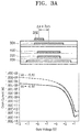
- FIGS. 3A through 3C are views illustrating relationships between the conductive layer 400 of FIG. 2A and the second gate electrode 302 of FIG. 2A in terms of location and voltage.
- FIGS. 3A to 3C illustrate only the first active layer 201, the first gate electrode 202, the conductive layer 400, the second active layer 301, and the second gate electrode 302.
- FIGS. 3A through 3C correspond to examples in which a gate voltage sweeping between 5V and -30V is applied to the first gate electrode 202, and a voltage of 9V is applied to the conductive layer 400.
- FIGS. 3A through 3C also illustrate graphs showing a relationship between a drain current and a gate voltage of the second TFT 300, when a drain voltage Vd of the second TFT 300 is -0.1V and -5.1V.
- FIGS. 3A through 3C correspond to a case where a center of the conductive layer 400 is aligned with that of the second active layer 301.
- a variation ⁇ Vth of a threshold voltage Vth in a saturation region of the second TFT 300 is about 0.18V.
- the variation ⁇ Vth of the threshold voltage Vth in the saturation region of the second TFT 300 is about 0.1V.
- the variation ⁇ Vth of the threshold voltage Vth in the saturation region of the second TFT 300 is about 0.25V.
- Table 2 shows variations ⁇ Vth of the threshold voltage Vth in the saturation region of the second TFT 300 when voltages of the conductive layer 400 are -2V, oV, and 9V, in the examples of FIGS. 3A through 3C .
- [Table 2] 2 ⁇ m (to the left side) 0 ⁇ m 2 ⁇ m (to the right side) -2V 0.2V 0.08V 0.26V 0V 0.2V 0.1V 0.27V 9V 0.18V 0.1V 0.25V
- an influence from a shift in location of the second gate electrode 302 relative to the conductive layer 400 to the threshold voltage Vth of the second TFT 300 is greater than an influence of a voltage of the conductive layer 400 to the threshold voltage Vth of the second TFT 300.
- a range of misalignment between the conductive layer 400 and the second gate electrode 302 may be set, such that the variation ⁇ Vth of the threshold voltage Vth of the second TFT 300 becomes less than 0.44V which is obtained based on a threshold voltage distribution of the second TFT 300.
- the misalignment may be a distance between the center of the conductive layer 400 and the center of the second gate electrode 302.
- the range of the misalignment between the conductive layer 400 and the second gate electrode 302 may be about 0 to about 3 ⁇ m.
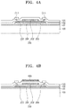
- FIGS. 4A through 8 are cross-sectional views schematically illustrating a method of manufacturing a semiconductor device according to an exemplary embodiment.
- the first TFT 200 may be formed on the substrate 100.
- the first buffer layer 101 may be disposed on the substrate 100.
- the substrate 100 may be formed of any of various materials, such as glass, plastic, or metal. According to an exemplary embodiment, the substrate 100 may be a flexible substrate. As used herein, the flexible substrate may refer a substrate that may be easily bent, folded, or rolled. The flexible substrate may be formed of ultra-thin glass, metal, or plastic.
- the first buffer layer 101 may block impurities from permeating through the substrate 100 and planarize the surface of the substrate 100.
- the first buffer layer 101 may include an inorganic material, such as silicon nitride (SiN x ) and/or silicon oxide (SiO x ), and may have a single-layered or a multi-layered structure. According to an exemplary embodiment, the first buffer layer 101 may be omitted.
- a semiconductor layer may be formed on the first buffer layer 101, and then patterned to be formed as the first active layer 201 of the first TFT 200.
- the semiconductor layer may include various materials.
- the semiconductor layer may include an inorganic semiconductor material, such as amorphous silicon or crystalline silicon.
- the semiconductor layer may include an oxide semiconductor or an organic semiconductor material.
- a first insulating layer 102 may be formed on the substrate 100 to cover the first active layer 201.
- the first insulating layer 102 may be an inorganic insulation layer.
- the first insulating layer 102 may be formed of at least one insulating material including SiO x , SiN x , silicon oxynitride (SiON), Al 2 O 3 , TiO 2 , Ta 2 O 5 , HfO 2 , ZrO 2 , BST, and PZT, and have a single-layered or a multi-layered structure.
- the first gate electrode 202 may be formed on the first insulating layer 102.
- the first gate electrode 202 may be formed of various conductive materials.
- the first gate electrode 202 may include at least one of aluminum (Al), platinum (Pt), palladium (Pd), silver (Ag), magnesium (Mg), gold (Au), nickel (Ni), neodymium (Nd), iridium (Ir), chromium (Cr), calcium (Ca), molybdenum (Mo), titanium (Ti), tungsten (W), and copper (Cu), and have a single-layered or a multi-layered structure.
- the first gate electrode 202 may overlap at least a portion of the first active layer 201.
- the first active layer 201 may be doped with B or P ion impurities. Accordingly, the first active layer 201 may include a source region doped with impurities, a drain region doped with impurities, and a channel region between the source and drain regions.
- a second insulating layer 103 may be formed on the first gate electrode 202.
- the second insulating layer 103 may be an inorganic insulation layer.
- the second insulating layer 103 may include at least one insulating material of SiO x , SiN x , SiON, Al 2 O 3 , TiO 2 , Ta 2 O 5 , HfO 2 , ZrO 2 , BST, and PZT, and have a single-layered or a multi-layered structure.
- the second insulating layer 103 may be an organic insulating layer.
- the first insulating layer 102 and the second insulating layer 103 may be patterned to form contact holes CH1 therein, respectively, exposing portions of the source region and the drain region of the first active layer 201.
- the first source electrode 203 and the first drain electrode 204 may be formed on the second insulating layer 103.
- the first source electrode 203 and the first drain electrode 204 may be formed of various conductive materials.
- each of the first source electrode 203 and the first drain electrode 204 may include at least one of aluminum (Al), platinum (Pt), palladium (Pd), silver (Ag), magnesium (Mg), gold (Au), nickel (Ni), neodymium (Nd), iridium (Ir), chromium (Cr), calcium (Ca), molybdenum (Mo), titanium (Ti), tungsten (W), and copper (Cu), and have a single-layered or a multi-layered structure.
- the first source electrode 203 and the first drain electrode 204 may include the same or different materials forming the first gate electrode 202.
- the first source electrode 203 and the first drain electrode 204 may respectively contact the source region and the drain region of the first active layer 201 via the contact holes CH1.
- the conductive layer 400 may be further formed on the second insulating layer 103.
- the conductive layer 400 may include at least one of aluminum (Al), platinum (Pt), palladium (Pd), silver (Ag), magnesium (Mg), gold (Au), nickel (Ni), neodymium (Nd), iridium (Ir), chromium (Cr), calcium (Ca), molybdenum (Mo), titanium (Ti), tungsten (W), and copper (Cu), and have a single-layered or a multi-layered structure.
- the conductive layer 400 may include the same or different materials forming the first gate electrode 202, the first source electrode 203, and the first drain electrode 204. In particular, the conductive layer 400 may be formed simultaneously with the first source electrode 203 and the first drain electrode 204, or may be formed in a separate process from a process of forming the first source electrode 203 and the first drain electrode 204.
- a third insulating layer 104a and a fourth insulating layer 105a may be sequentially formed on the substrate 100 to cover the conductive layer 400. Due to a structure of the first TFT 200 below the third insulating layer 104a, the third insulating layer 104a may have a step ⁇ H formed by a convex portion and a concave portion thereof.
- the third insulating layer 104a may include at least one insulating material of SiO x , SiN x , SiON, Al 2 O 3 , TiO 2 , Ta 2 O 5 , HfO 2 , ZrO 2 , BST, and PZT, and have a single-layered or a multi-layered structure.
- the fourth insulating layer 105a may include at least one insulating material of SiO x , SiN x , SiON, Al 2 O 3 , TiO 2 , Ta 2 O 5 , HfO 2 , ZrO 2 , BST, and PZT, and have a single-layered or a multi-layered structure.
- a material used to form the fourth insulating layer 105a may be different from that of the third insulating layer 104a.
- the material used to form the fourth insulating layer 105a may be different from that used to form an upper portion of the third insulating layer 104a.
- the third insulating layer 104a may be an insulating layer including SiO x , or a multi-layer of a lower insulating layer including SiO x and an upper insulating layer including SiN x .
- the fourth insulating layer 105a may be an insulating layer including SiO x .
- a portion of the fourth insulating layer 105a may be removed to expose an upper surface of the third insulating layer 104a, thereby forming the planarization layer PAV including the third insulating layer 104 and the fourth insulating layer 105.
- a portion of the third insulating layer 104a may also be removed.
- the fourth insulation layer 105a may be removed by any of various etching processes.
- an etching process may include dry etching or a polishing process, such as chemical mechanical polishing (CMP).
- CMP is a technique of planarizing the surface of a to-be-processed product by using chemical and mechanical actions.
- slurry is supplied to cause chemical reaction with the surface of the to-be-processed product, during which a platen and the polishing head move relative to each other to mechanically planarize the surface of the to-be-processed product.
- the third insulating layer 104a has a convex portion and the concave portion due to the first TFT 200 and the conductive layer 400 formed below the third insulating layer 104a.
- the etching process described above may cause the concave portion of the third insulating layer 104a to be filled with the fourth insulating layer 105a.
- the upper surface of the third insulating layer 104 and the upper surface of the fourth insulating layer 105 may be substantially flush with each other, thereby generally forming a flat upper surface. Accordingly, an influence from a lower wiring pattern to upper layers to be formed later may be reduced, thereby improving coverage of the upper layers.
- a step ⁇ H' of the third insulating layer 104 may be less than or equal to the step ⁇ H of the third insulating layer 104a shown in FIG. 5 .
- the second buffer layer 106 may be formed on the flat upper surface of the third and fourth insulating layers 104 and 105.
- the second buffer layer 106 may include at least one insulating material of SiO x , SiN x , SiON, Al 2 O 3 , TiO 2 , Ta 2 O 5 , HfO 2 , ZrO 2 , BST, and PZT, and have a single-layered or a multi-layered structure.
- the second buffer layer 106 may be an insulating layer including SiO x , more specifically, SiO 2 .
- the second buffer layer 106 may be a multi-layered insulating layer including a lower insulating layer including SiO 2 and an upper insulating layer including SiON.
- the second buffer layer 106 and the planarization layer PAV may undergo thermal treatment.
- the thermal treatment may include dehydrogenation treatment.
- the second buffer layer 106 may perform a barrier function of preventing hydrogen H2 generated from lower insulating layers from spreading to an upper layer.
- the second TFT 300 may be formed on the second buffer layer 106. More particularly, a semiconductor layer may be formed on the second buffer layer 106, and then patterned to be formed as the second active layer 301 of the second TFT 300.
- the semiconductor layer may include various materials.
- the semiconductor layer may include an inorganic semiconductor material, such as amorphous silicon or crystalline silicon.
- the semiconductor layer may include an oxide semiconductor or an organic semiconductor material.
- the semiconductor layer may be crystallized via excimer laser annealing (ELA).
- the thickness of the second active layer 301 may be about 80% or less than that of the first active layer 201.
- the second active layer 301 is formed to have a small thickness, such that ELA crystallization is performed with a laser energy band that does not affect the lower layer.
- a lower limit of the thickness of the second active layer 301 may be determined in consideration of the characteristics of a device, such as the first TFT 200 and/or the second TFT 300.
- a fifth insulating layer 107 may be formed on the second buffer layer 106 to cover the second active layer 301.
- the fifth insulating layer 107 may be an inorganic insulation layer.
- the fifth insulating layer 107 may include at least one insulating material of SiO x , SiN x , SiON, Al 2 O 3 , TiO 2 , Ta 2 O 5 , HfO 2 , ZrO 2 , BST, and PZT, and have a single-layered or a multi-layered structure.
- the second gate electrode 302 may be formed on the fifth insulating layer 107.
- the second gate electrode 302 may be formed of various conductive materials.
- the second gate electrode 302 may include at least one of aluminum (Al), platinum (Pt), palladium (Pd), silver (Ag), magnesium (Mg), gold (Au), nickel (Ni), neodymium (Nd), iridium (Ir), chromium (Cr), calcium (Ca), molybdenum (Mo), titanium (Ti), tungsten (W), and copper (Cu), and have a single-layered or a multi-layered structure.
- the second gate electrode 302 may overlap at least a portion of the second active layer 301.
- the second active layer 301 may be doped with B or P ion impurities. Accordingly, the second active layer 301 may include a source region doped with impurities, a drain region doped with impurities, and a channel region between the source and drain regions.
- a sixth insulating layer 108 may be formed on the second gate electrode 302.
- the sixth insulating layer 108 may be an inorganic insulating layer.
- the sixth insulating layer 108 may include at least one insulating material of SiO x , SiN x , SiON, Al 2 O 3 , TiO 2 , Ta 2 O 5 , HfO 2 , ZrO 2 , BST, and PZT, and have a single-layered or a multi-layered structure.
- the sixth insulating layer 108 may be an organic insulating layer.
- the fifth insulating layer 107 and the sixth insulating layer 108 may be patterned to include contact holes CH2 therein, respectively, which expose portions of the source region and the drain region of the second active layer 301.
- the second source electrode 303 and the second drain electrode 304 may be formed on the sixth insulating layer 108.
- the second source electrode 303 and the second drain electrode 304 may be formed of various conductive materials.
- each of the second source electrode 303 and the second drain electrode 304 may include at least one of aluminum (Al), platinum (Pt), palladium (Pd), silver (Ag), magnesium (Mg), gold (Au), nickel (Ni), neodymium (Nd), iridium (Ir), chromium (Cr), calcium (Ca), molybdenum (Mo), titanium (Ti), tungsten (W), and copper (Cu), and have a single-layered or a multi-layered structure.
- the second source electrode 303 and the second drain electrode 304 may include the same or different materials forming the second gate electrode 302.
- the second source electrode 303 and the second drain electrode 304 may contact the source region and the drain region of the second active layer 301 via the contact holes CH2, respectively.
- a seventh insulating layer 109 may be formed on the substrate 100 to cover the second source electrode 303 and the second drain electrode 304.
- the seventh insulating layer 109 may include at least one inorganic insulating material of SiO x , SiN x , SiON, Al 2 O 3 , TiO 2 , Ta 2 O 5 , HfO 2 , ZrO 2 , BST, and PZT, and have a single-layered or a multi-layered structure.
- the seventh insulation layer 109 may include at least one organic insulating material of a commercial polymer, such as polymethyl methacrylate (PMMA) or polystyrene (PS), a polymer derivative having a phenol group, an acryl-based polymer, an imide-based polymer, an acryl ether-based polymer, an amide-based polymer, a fluorine-based polymer, a p-xylene-based polymer, a vinyl alcohol-based polymer, a blend thereof, or the like, and have a single-layered or a multi-layered structure.
- a commercial polymer such as polymethyl methacrylate (PMMA) or polystyrene (PS), a polymer derivative having a phenol group, an acryl-based polymer, an imide-based polymer, an acryl ether-based polymer, an amide-based polymer, a fluorine-based polymer, a p-xylene-based polymer, a vinyl alcohol-based polymer,
- FIG. 9 is a perspective view of a display apparatus 1 according to an exemplary embodiment.
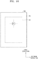
- FIG. 10 is a schematic plan view of the display apparatus 1.
- the display apparatus 1 includes a substrate 100, a display unit 130 disposed on the substrate 100, and an encapsulation member 150 covering the display unit 130.
- the substrate 100, the display unit 130, and the encapsulation member 150 are sequentially stacked on one another in a third direction.
- the display apparatus 1 may be a liquid crystal display (LCD), an organic light-emitting display, an electrophoretic display, an electrowetting display panel, or the like.
- LCD liquid crystal display
- OLED organic light-emitting display
- electrophoretic display an electrophoretic display
- electrowetting display panel an electrowetting display panel
- the substrate 100 includes a display area DA and a peripheral area PA around the display area DA.
- the display unit 130 may be formed in the display area DA.
- the display unit 130 may include a plurality of pixels PX arranged in a first direction and a second direction.
- Each pixel PX may include a display element, and a pixel circuit electrically connected to the display element.
- the pixel circuit may include at least one TFT and at least one capacitor.
- the encapsulation member 150 may include a substrate or at least one thin film stacked on the display unit 130. According to an exemplary embodiment, the encapsulation member 150 may include a plurality of thin films, which may prevent external moisture and/or air from permeating into the display unit 130.
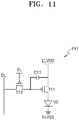
- FIG. 11 is a circuit diagram of a first pixel PX1 of the display apparatus 1 according to an exemplary embodiment.
- the first pixel PX1 may include a pixel circuit and a display element ED connected to the pixel circuit.
- the pixel circuit may include a first transistor T11, a second transistor T12, and a capacitor C11.
- the first transistor T11 includes a gate electrode connected to a second electrode of the second transistor T12, a first electrode that receives a first power supply voltage ELVDD, and a second electrode connected to the display element ED.
- the second transistor T12 includes a gate electrode connected to a scan line SL, a first electrode connected to a data line DL, and a second electrode connected to the gate electrode of the first transistor T11.
- the capacitor C11 includes a first electrode connected to the gate electrode of the first transistor T11 and the second electrode of the second transistor T12, and a second electrode that receives the first power supply voltage ELVDD.
- the display element ED may be connected to the pixel circuit via the first transistor T11.
- the display element ED may be an organic light-emitting diode (OLED).
- OLED includes a first electrode connected to the second electrode of the first transistor T11, a second electrode that receives a second power supply voltage ELVSS, and an emission layer disposed between the first electrode and the second electrode.
- the first power supply voltage ELVDD may be higher than the second power supply voltage ELVSS.
- FIG. 11 shows a pixel having a P-type transistor, however, embodiments of the inventive concept are not limited thereto, and a pixel may have an N-type transistor.
- FIG. 12 is a cross-sectional view of a portion of the first pixel PX1 of FIG. 11 .
- a first electrode and a second electrode of a transistor are interchangeably used as a source electrode and a drain electrode of a TFT.
- the first pixel PX1 may include the first TFT 200 and the second TFT 300 of the semiconductor device 10b described above, respectively.
- a process of manufacturing the first TFT 200 and the second TFT 300 is the same as the above-described process of manufacturing a semiconductor device.
- the first pixel PX1 of FIG. 12 may include the first TFT 200 and the second TFT 300 of the semiconductor device 10a shown in FIG. 1A .
- the first transistor T11 may be implemented using the first TFT 200.
- the first TFT 200 may include the first active layer 201, the first gate electrode 202, the first source electrode 203, and the first drain electrode 204.
- the first source electrode 203 and the first drain electrode 204 may be electrically connected to the source region and the drain region of the first active layer 201, respectively, via the contact holes CH1.
- the second transistor T12 may be implemented using the second TFT 300.
- the second TFT 300 may include the second active layer 301, the second gate electrode 302, the second source electrode 303, and the second drain electrode 304.
- the capacitor C11 may be implemented by using the first gate electrode 202 and the conductive layer 400 as the first and second electrodes, respectively.
- the first power supply voltage ELVDD which may have a constant voltage, may be applied to the conductive layer 400.
- the second active layer 301 and the second gate electrode 302 of the second TFT 300 may be disposed to at least partially overlap the conductive layer 400.
- the conductive layer 400 may be formed to be larger in size than the second gate electrode 302, so as to prevent affecting a back channel of the second TFT 300.
- the edge of the conductive layer 400 may extend beyond the edge of the second gate electrode 302 by about 1.5 ⁇ m or more. Accordingly, the conductive layer 400 may function as a shielding layer, and thus, may minimize an influence of a potential of a lower line and/or electrode, such as the first gate electrode 202, to the second TFT 300.
- the planarization layer PAV including the third insulating layer 104 and the fourth insulating layer 105 may be disposed between the first TFT 200 and the second TFT 300.
- the second buffer layer 106 may be disposed on the planarization layer PAV.
- the seventh insulating layer 109 may be disposed on the sixth insulating layer 108 to cover the second TFT 300.
- the third through seventh insulating layers 104 through 109 may include a contact hole CH 3 , by which a portion of one of the first source electrode 203 and the first drain electrode 204 of the first TFT 200 is exposed.
- FIG. 12 exemplarily shows that the first drain electrode 204 is exposed by the contact hole CH 3 .
- a connecting electrode 500 may be disposed on the seventh insulating layer 109 to fill the contact hole CH 3 .
- the connecting electrode 500 may contact the first drain electrode 204.
- the connecting electrode 500 may include at least one of aluminum (Al), platinum (Pt), palladium (Pd), silver (Ag), magnesium (Mg), gold (Au), nickel (Ni), neodymium (Nd), iridium (Ir), chromium (Cr), calcium (Ca), molybdenum (Mo), titanium (Ti), tungsten (W), and copper (Cu), and have a single-layered or a multi-layered structure.
- An eighth insulating layer 110 may be disposed on the seventh insulating layer 109 to cover the connecting electrode 500.
- the eighth insulating layer 110 may have single layered or a multi-layered structure formed of an organic insulating material.
- the eighth insulation layer 110 may include a commercial polymer, such as PMMA or PS, a polymer derivative having a phenol group, an acryl-based polymer, an imide-based polymer, an acryl ether-based polymer, an amide-based polymer, a fluorine-based polymer, a p-xylene-based polymer, a vinyl alcohol-based polymer, a blend thereof, or the like.
- the eighth insulating layer 110 may include polyimide, polyamide (PA), acryl resin, or the like.
- the eighth insulating layer 110 may function as a planarization layer having a flat upper surface.
- the eighth insulating layer 110 may include a via hole VIA that exposes a portion of the connecting electrode 500.
- a display element 600 (display element ED in FIG. 11 ) may be disposed on the eighth insulating layer 110.
- the display element 600 may include a first electrode 601, a second electrode 603 opposite to the first electrode 601, and an intermediate layer 602 disposed between the first electrode 601 and the second electrode 603.
- the first electrode 601 may fill the via hole VIA and contact the connecting electrode 500. Accordingly, the first electrodes 601 may be electrically connected to the first TFT 200.
- a ninth insulating layer 111 may be disposed on the eighth insulating layer 110 to cover an edge of the first electrode 601.
- the ninth insulating layer 111 may include at least one inorganic insulating material of SiO x , SiN x , SiON, Al 2 O 3 , TiO 2 , Ta 2 O 5 , HfO 2 , ZrO 2 , BST, and PZT, and have a single-layered or a multi-layered structure.
- the ninth insulation layer 111 may include at least one organic insulating material of a commercial polymer (such as PMMA or PS), a polymer derivative having a phenol group, an acryl-based polymer, an imide-based polymer, an acryl ether-based polymer, an amide-based polymer, a fluorine-based polymer, a p-xylene-based polymer, a vinyl alcohol-based polymer, a blend thereof, or the like, and have a single-layered or a multi-layered structure.
- a commercial polymer such as PMMA or PS
- the first electrode 601 may include a reflective layer including a reflective conductive material, such as silver (Ag), magnesium (Mg), aluminum (Al), platinum (Pt), palladium (Pd), gold (Au), nickel (Ni), neodymium (Nd), iridium (Ir), chromium (Cr), or a compound thereof.
- the first electrode 601 may include at least one transparent conductive oxide of indium tin oxide (ITO), indium zinc oxide (IZO), zinc oxide (ZnO), indium oxide (In 2 O 3 ), indium gallium oxide (IGO), and aluminum zinc oxide (AZO).
- the first electrode 601 may be a stack of the reflective layer and the transparent conductive layer.
- the intermediate layer 602 including an emission layer may be formed on the first electrode 601.
- the emissive layer may include a low-molecular weight organic material or a high-molecular weight organic material.
- the display element 600 may emit red light, green light, or blue light, depending on the type of emission layer.
- a plurality of organic emission layers may be disposed on a single display element 600.
- a plurality of organic emission layers respectively emitting light of red, green, and blue colors may be stacked or mixed vertically to emit white color light.
- the display apparatus 1 may further include a color converting layer or a color filter that coverts the white light into a light of a predetermined color.
- the red, green, and blue colors are exemplary, and thus a color combination for emitting white light is not limited thereto in embodiments of the invention.
- the intermediate layer 602 may include at least one functional layer of a hole injection layer (HIL), a hole transport layer (HTL), an electron transport layer (ETL), and an electron injection layer (EIL) between the first electrode 601 and the emission layer and/or between the emission layer and the second electrode 603.
- HIL hole injection layer
- HTL hole transport layer
- ETL electron transport layer
- EIL electron injection layer
- FIG. 12 shows that the intermediate layer 602 is patterned to correspond to only the first electrode 601, embodiments of the inventive concept are not limited thereto, and the intermediate layer 602 may be integrally formed with an intermediate layer 602 of a pixel adjacent to the first pixel PX1. Alternatively, at least one layer of the intermediate layer 602 may be formed for each pixel, and the other layers thereof may be integrally formed with the intermediate layer 602 of the adjacent pixel.
- the second electrode 603 may be formed on the intermediate layer 602 over the entire area of the display region DA of the substrate 100.
- the second electrode 603 may include various conductive materials.
- the second electrode 603 may include a semi-transparent reflection layer including at least one of lithium (Li), calcium (Ca), lithium fluoride (LiF), aluminum (Al), magnesium (Mg), and silver (Ag), or may include a light-transmitting metal oxide, such as ITO, IZO, or ZnO, and may have a single layered or a multi-layered structure.
- the display element 600 is disposed to overlap the first TFT 200 and the second TFT 300 below the display element 600.
- the display element 600 may be disposed to not overlap or at least partially overlap the first TFT 200 and the second TFT 300.
- FIG. 13 is a circuit diagram of a second pixel PX2 of the display apparatus 1 according to another exemplary embodiment.
- the second pixel PX2 may include a pixel circuit and a display element ED connected to the pixel circuit.
- the pixel circuit may include a first transistor T21, a second transistor T22, a third transistor T23, a first capacitor C21, and a second capacitor C22.
- the first transistor T21 includes a gate electrode connected to a first electrode of the second transistor T22, a first electrode that receives a first power supply voltage ELVDD, and a second electrode connected to the display element ED.
- the second transistor T22 includes a gate electrode connected to the scan line SL, a first electrode connected to the gate electrode of the first transistor T21, and a second electrode connected to the second electrode of the first transistor T21.
- the third transistor T23 includes a gate electrode connected to the control line CL, a first electrode that receives an initializing voltage VINT, and a second electrode connected to the second electrode of the first transistor T21 and the second electrode of the second transistor T22.
- the first capacitor C21 includes a first electrode connected to the data line DL, and a second electrode connected to the second electrode of the first transistor T21.
- the first capacitor C21 may store a data voltage applied to the data line DL.
- the second capacitor C22 includes a first electrode that receives the initializing voltage VINT, and a second electrode connected to the gate electrode of the first transistor T21.
- the display element ED may be connected to the pixel circuit via the first transistor T21.
- the display element ED may be an OLED.
- the OLED includes a first electrode connected to the second electrode of the first transistor T21, a second electrode that receives a second power supply voltage ELVSS, and an emission layer disposed between the first electrode and the second electrode.
- the first power supply voltage ELVDD may be higher than the second power supply voltage ELVSS.
- the second pixel PX2 may be operated according to a first period of initializing the first electrode of the display element ED, a second period of compensating for a threshold voltage of the first transistor T21, a third period of writing a data voltage, and a fourth period during which the display element ED emits light.
- the second transistor T22 and the third transistor T23 are turned on, and thus, the first electrode of the display element ED may be initialized to the initializing voltage VINT.
- the second transistor T22 is turned on, and accordingly, the first transistor T21 is diode-connected, and thus, a threshold voltage of the first transistor T21 may be compensated for.
- the second transistor T22 is turned on and the first transistor T21 and the third transistor T23 are turned off, and thus, the first capacitor C21 and the second capacitor C22 may be serially connected to each other at a node N.
- the data voltage may be applied to the data line DL. Accordingly, the data voltage is distributed to the first capacitor C21 and the second capacitor C22, and a distributed voltage may be applied to the node N.
- the first transistor T21 is turned on.
- the display element ED may emit light.
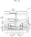
- FIGS. 14 and 15 are cross-sectional views of portions of the second pixel PX2 of FIG. 13 according to exemplary embodiments.
- a first electrode and a second electrode of a transistor are interchangeably used as a source electrode and a drain electrode of a TFT.
- a second pixel PX2a may include the first TFT 200 and the second TFT 300 of the above-described semiconductor device 10b.
- the second pixel PX2a of FIG. 14 may include the first TFT 200 and the second TFT 300 of the semiconductor device 10a shown in FIG. 1A .
- the first transistor T21 may be implemented using the first TFT 200.
- the first TFT 200 may include the first active layer 201, the first gate electrode 202, the first source electrode 203, and the first drain electrode 204.
- the first source electrode 203 and the first drain electrode 204 may be electrically connected to the source region and the drain region of the first active layer 201, respectively, via the contact holes CH1.
- the second transistor T22 may be implemented using the second TFT 300.
- the second TFT 300 may include the second active layer 301, the second gate electrode 302, the second source electrode 303, and the second drain electrode 304.
- the second source electrode 303 and the second drain electrode 304 may correspond to the source region and the drain region of the second active layer 301, respectively.
- the second source electrode 303 of the second TFT 300 may be electrically connected to the first gate electrode 202 of the first TFT 200 via connecting electrodes 501 and 502.
- the connecting electrode 501 may be formed on the second insulating layer 103 and may contact a portion of the first gate electrode 202 exposed via a contact hole CH 4 formed in the second insulating layer 103.
- the connecting electrode 502 may be formed on the sixth insulating layer 108, and may contact a portion of the connecting electrode 501 and a portion of the second source electrode 303 that are exposed via a contact hole CH 5 formed in the third through sixth insulating layers 104 through 108.
- the planarization layer PAV including the third insulating layer 104 and the fourth insulating layer 105 may be disposed between the first TFT 200 and the second TFT 300.
- the second buffer layer 106 may be disposed on the planarization layer PAV.
- the third transistor T23 may be implemented using a third TFT 700.
- the third TFT 700 may include a third active layer 701, a third gate electrode 702, a third source electrode 703, and a third drain electrode 704.
- the third active layer 701 may extend from the first active layer 201.
- the third source electrode 703 and the third drain electrode 704 may be electrically connected to a source region and a drain region of the third active layer 701, respectively, which are exposed via the contact holes CH1.
- the third drain electrode 704 of the third TFT 700 may be the first drain electrode 204 of the first TFT 200.
- the first capacitor C21 may be implemented using a capacitor 800 including a first electrode 801 and a second electrode 802.
- the first electrode 801 may be formed on a second seventh insulating layer 109b, and the second electrode 802 may be formed on a third seventh insulating layer 109C.
- Each of the first electrode 801 and the second electrode 802 may include at least one of aluminum (Al), platinum (Pt), palladium (Pd), silver (Ag), magnesium (Mg), gold (Au), nickel (Ni), neodymium (Nd), iridium (Ir), chromium (Cr), calcium (Ca), molybdenum (Mo), titanium (Ti), tungsten (W), and copper (Cu), and have a single-layered or a multi-layered structure.
- each of the first and second electrodes 801 and 802 may have a three-layered structure of Ti/Al/Ti.
- the second capacitor C22 may be implemented by using the first gate electrode 202 and the conductive layer 400 as the first and second electrodes, respectively.
- the first source electrode 203 of the first TFT 200 may be electrically connected to a first power line 901 that applies the first power supply voltage ELVDD.
- the first power line 901 may be formed on a first seventh insulating layer 109a, and may contact a portion of the first source electrode 203 exposed via a contact hole CH6 formed in the third through first seventh insulating layers 104 through 109a.
- the first drain electrode 204 of the first TFT 200 and the third drain electrode 704 of the third TFT 700 may be electrically connected to the second electrode 802 of the first capacitor C21 via a contact hole CH7 formed in the third through third seventh insulating layers 104 through 109C.
- the second drain electrode 304 of the second TFT 300 may be electrically connected to the second electrode 802 of the first capacitor C21 via a contact hole CH8 formed in the fifth through third seventh insulating layers 107 through 109C.
- the third gate electrode 702 of the third TFT 700 may be electrically connected to a control line 902 by using a connecting electrode 503.
- the connecting electrode 503 may be formed on the second insulating layer 103, and may contact a portion of the third gate electrode 702 exposed via a contact hole CH9 formed in the second insulating layer 103.
- the control line 902 may be formed on the sixth insulating layer 108, and may contact a portion of the connecting electrode 503 exposed via a contact hole CH10 formed in the third through sixth insulating layers 104 through 108.
- the third source electrode 703 of the third TFT 700 may be electrically connected to a second power line 903 that applies the initializing voltage VINT, by using a connecting electrode 504.
- the connecting electrode 504 may be formed on the sixth insulating layer 108, and may contact a portion of the third source electrode 703 exposed via a contact hole CH11 formed in the third through sixth insulating layers 104 through 108.
- the second power line 903 may be formed on the first seventh insulating layer 109a, and may contact a portion of the connecting electrode 504 exposed via a contact hole CH12 formed in the first seventh insulating layer 109a.
- An eighth insulating layer 110 may be disposed on the third seventh insulating layer 109c to cover the capacitor 800.
- the eighth insulating layer 110 may include a via hole VIA that exposes a portion of the second electrode 802 of the capacitor 800.
- the display element 600 (display element ED in FIG. 13 ) may be disposed on the eighth insulating layer 110.
- the display element 600 may include the first electrode 601, the second electrode 603 opposite to the first electrode 601, and the intermediate layer 602 disposed between the first electrode 601 and the second electrode 603.
- the first seventh insulating layer 109a, the second seventh insulating layer 109b, and the third seventh insulating layer 109c may include at least one inorganic insulating material of SiO x , SiN x , SiON, Al 2 O 3 , TiO 2 , Ta 2 O 5 , HfO 2 , ZrO 2 , BST, and PZT, and have a single-layered or a multi-layered structure.
- the first seventh insulating layer 109a, the second seventh insulating layer 109b, and the third seventh insulating layer 109c may include at least one organic insulating material of a commercial polymer (such as PMMA or PS), a polymer derivative having a phenol group, an acryl-based polymer, an imide-based polymer, an acryl ether-based polymer, an amide-based polymer, a fluorine-based polymer, a p-xylene-based polymer, a vinyl alcohol-based polymer, a blend thereof, or the like, and have a single-layered or a multi-layered structure.
- a commercial polymer such as PMMA or PS
- the connecting electrodes 501 through 504, the first power line 901, the control line 902, and the second power line 903 may each include at least one of aluminum (Al), platinum (Pt), palladium (Pd), silver (Ag), magnesium (Mg), gold (Au), nickel (Ni), neodymium (Nd), iridium (Ir), chromium (Cr), calcium (Ca), molybdenum (Mo), titanium (Ti), tungsten (W), and copper (Cu), and each have a single-layered or a multi-layered structure.
- a second pixel PX2b of FIG. 15 is different from the second pixel PX2a of FIG. 14 in that a planarization layer is formed on an insulating layer between the second TFT 300 and the display element 600.
- the differences between the second pixel PX2b of FIG. 15 and the second pixel PX2a of FIG. 14 will mainly be described.
- the second pixel PX2b of FIG. 15 may include the first TFT 200 and the second TFT 300 of the semiconductor device 10a shown in FIG. 1A .
- a first insulating layer and a second insulating layer may be sequentially stacked on the first seventh insulating layer 109a, and then a portion of the second insulating layer may be removed to expose an upper surface of the first insulating layer, thereby forming a planarization layer including a first second seventh insulating layer 109b1 and a second second seventh insulating layer 109b2. While the second insulating layer is being removed, a portion of the first insulating layer may also be removed.
- the second insulating layer may be removed by any of various etching processes.
- an etching process may include dry etching or a polishing process, such as CMP.
- the second second seventh insulating layer 109b2 may be disposed on the first second seventh insulating layer 109b1, and an upper surface of the first second seventh insulating layer 109b1 and an upper surface of the second second seventh insulating layer 109b2 may be substantially flush with each other, thereby forming an entirely-flat upper surface.
- a third buffer layer 109b3 may be disposed on the first second seventh insulating layer 109b1 and the second second seventh insulating layer 109b2.
- the first capacitor 800 may be disposed on the third buffer layer 109b3.
- a step difference between the insulating layers may be increased.
- an excessive step difference between a plurality of insulating layers, due to lower lines and/or electrodes, may be reduced by including a planarization layer in between the insulating layers, which may improve the coverage of a layer and/or line to be formed on the planarization layer.
- the first second seventh insulating layer 109b1 and the second second seventh insulating layer 109b2 may include at least one inorganic insulating material of SiO x , SiN x , SiON, Al 2 O 3 , TiO 2 , Ta 2 O 5 , HfO 2 , ZrO 2 , BST, and PZT, and have a single-layered or a multi-layered structure.
- the first second seventh insulating layer 109b1 and the second second seventh insulating layer 109b2 may include at least one organic insulating material of a commercial polymer (such as PMMA or PS), a polymer derivative having a phenol group, an acryl-based polymer, an imide-based polymer, an acryl ether-based polymer, an amide-based polymer, a fluorine-based polymer, a p-xylene-based polymer, a vinyl alcohol-based polymer, a blend thereof, or the like, and have a single-layered or a multi-layered structure.
- a commercial polymer such as PMMA or PS
- a material used to form the second second seventh insulating layer 109b2 may be different from that used to form the first second seventh insulating layer 109b1.
- a material used to form the second second seventh insulating layer 109b2 may be different from that used to form an upper portion of the first second seventh insulating layer 109b1.
- the first second seventh insulating layer 109b1 may be an insulating layer including SiO x , or a multi-layer of a lower insulating layer including SiO x and an upper insulating layer including SiN x .
- the second second seventh insulating layer 109b2 may be an insulating layer including SiO x .
- the third buffer layer 109b3 may include at least one insulating material of SiO x , SiN x , SiON, Al 2 O 3 , TiO 2 , Ta 2 O 5 , HfO 2 , ZrO 2 , BST, and PZT, and have a single-layered or a multi-layered structure.
- the third buffer layer 109b3 may be an insulating layer including SiN x .
- the third buffer layer 109b3, and a planarization layer of the first second seventh insulating layer 109b1 and the second second seventh insulating layer 109b2 may optionally undergo thermal treatment.
- the thermal treatment may include dehydrogenation treatment.
- FIG. 15 shows that two planarization layers are formed.
- embodiments of the inventive concept are not limited thereto, and more than two planarization layers may be formed according to positions or arrangements of lines and/or electrodes that constitute a pixel.
- the conductive layer 400 is disposed below the second TFT 300, as an electrode of the capacitors C11 and C22, to which a constant power supply voltage is applied.
- embodiments of the inventive concepts are not limited thereto.
- the conductive layer 400 may be a line and/or electrode, to which a constant DC voltage is applied during at least one of a threshold voltage compensating time period, a data write time period, and a light-emitting time period within a pixel driving time period.
- a display apparatus comprising: a first thin film transistor disposed over a substrate and comprising a first active layer; a second thin film transistor disposed over the first thin film transistor and comprising a second active layer overlapping the first thin film transistor; a first planarization layer disposed between the first thin film transistor and the second thin film transistor, the first planarization layer comprising a first insulating layer and a second insulating layer disposed over the first insulating layer; and a first buffer layer disposed between the first planarization layer and the second thin film transistor, wherein an upper surface of the second insulating layer and an upper surface of the first insulating layer are substantially flush with each other.
- a portion of the first insulating layer is disposed over the first thin film transistor and a portion of the second insulating layer is disposed adjacent the first thin film transistor.
- a portion of the first insulating layer is may overlap the first thin film transistor and a portion of the second insulating layer may overlap a region adjacent the first thin film transistor.
- a material used to form the second insulating layer may be different from that of the first insulating layer.
- the first insulating layer may be an insulating layer including SiOx, or a multi-layer of a lower insulating layer including SiOx and an upper insulating layer including SiNx.
- the second insulating layer may be an insulating layer including SiOx.
- the display apparatus may comprise a conductive layer disposed between the first thin film transistor and the first planarization layer and overlapping the second active layer.
- the display apparatus may be configured to apply a direct current (DC) voltage to the conductive layer.
- a size of the conductive layer may be greater than a size of a gate electrode of the second thin film transistor.
- the conductive layer may, in some embodiments, be located between the source and drain electrodes of the first thin film transistor.
- the conductive layer may, in some embodiments, have a width that is smaller than the width of the first thin film transistor,
- Embodiments of the invention may provide a method of manufacturing a display apparatus, the method comprising: forming a first thin film transistor over a substrate, the first thin film transistor comprising a first active layer; forming, over the first thin film transistor, a first insulating layer and a second insulating layer; forming a first planarization layer by etching the second insulating layer, such that an upper surface of the first insulating layer and an upper surface of the second insulating layer are substantially flush with each other; forming a first buffer layer over the first planarization layer; and forming a second thin film transistor on over the first buffer layer, the second thin film transistor comprising a second active layer overlapping the first thin film transistor.
- the method may comprise: forming the first insulating layer so as to overlap the first thin film transistor and a region adjacent the first thin film transistor; forming the second insulating layer over so as to overlap the first thin film transistor and a region adjacent the first thin film transistor; and then etching the second insulating layer so that the upper surface of the first insulating layer and the upper surface of the second insulating layer are substantially flush with each other.
- display apparatuses may be capable of realizing high-resolution by the above described arrangement of the elements of TFTs within a pixel.
Landscapes
- Engineering & Computer Science (AREA)
- Microelectronics & Electronic Packaging (AREA)
- Physics & Mathematics (AREA)
- Geometry (AREA)
- Manufacturing & Machinery (AREA)
- Optics & Photonics (AREA)
- Thin Film Transistor (AREA)
- Electroluminescent Light Sources (AREA)
- Devices For Indicating Variable Information By Combining Individual Elements (AREA)
Abstract
Description
- Exemplary embodiments of the invention relate generally to a display apparatus and a method of manufacturing the same.
- Display apparatuses include a display device and electronic devices for controlling an electrical signal applied to the display device. The electronic devices include a thin film transistor (TFT), a capacitor, and a plurality of lines.
- As the resolution of display apparatuses and the number of TFTs electrically connected to a single display device are increased, a pixel aperture ratio may be decreased.
- The above information disclosed in this Background section is only for understanding of the background of the inventive concepts, and, therefore, it may contain information that does not constitute prior art.
- Devices constructed according to exemplary embodiments of the invention are capable of realizing high resolution.
- Additional aspects will be set forth in part in the description which follows and, in part, will be apparent from the description, or may be learned by practice of the presented embodiments.
- A display apparatus according to an exemplary embodiment includes a first thin film transistor disposed on a substrate and including a first active layer, a second thin film transistor disposed on the first thin film transistor and including a second active layer overlapping the first thin film transistor, a first planarization layer disposed between the first thin film transistor and the second thin film transistor, the first planarization layer including a first insulating layer and a second insulating layer disposed on the first insulating layer, and a first buffer layer disposed between the first planarization layer and the second thin film transistor, in which an upper surface of the second insulating layer and an upper surface of the first insulating layer are substantially flush with each other.
- The first buffer layer may include silicon oxide.
- The display apparatus may further include a conductive layer disposed between the first thin film transistor and the first planarization layer and overlapping the second active layer.
- The conductive layer may be configured to be applied with a direct current (DC) voltage.
- At least a light-emitting section of the conductive layer may be configured to be applied with a DC voltage.
- A size of the conductive layer may be larger than a size of the gate electrode of the second thin film transistor.
- A center of the conductive layer may be shifted from a center of a gate electrode of the second thin film transistor a distance of less than 3 µm.
- A thickness of the second active layer may be less than a thickness of the first active layer.
- A thickness of the second active layer may be less than or equal to 80% of a thickness of the first active layer.
- The display apparatus may further include a display device disposed on the second thin film transistor, the display device overlapping the second thin film transistor and connected to the first thin film transistor.
- The display apparatus may further include, between the second thin film transistor and the display device, a second planarization layer including a third insulating layer and a fourth insulating layer disposed on the third insulating layer, and a second buffer layer on the second planarization layer, in which an upper surface of the fourth insulating layer and as an upper surface of the third insulating layer are substantially flush with each other.
- The display apparatus may further include a fifth insulating layer disposed between the second thin film transistor and the display device.
- The second buffer layer may include silicon nitride.
- The display apparatus may further include a third thin film transistor including a third active layer extending from the first active layer.
- The display apparatus may further include a capacitor disposed on the second thin film transistor and at least partially overlapping the second active layer.
- A method of manufacturing a display apparatus according to an exemplary embodiment includes forming a first thin film transistor including a first active layer on a substrate, forming, on the first thin film transistor, a first insulating layer and a second insulating layer, forming a first planarization layer by etching the second insulating layer such that an upper surface of the first insulating layer and an upper surface of the second insulating layer are substantially flush with each other, forming a first buffer layer on the first planarization layer, and forming a second thin film transistor on the first buffer layer, the second thin film transistor including a second active layer overlapping the first thin film transistor.
- The method may further include performing thermal treatment on the first planarization layer and the first buffer layer before forming the second thin film transistor.
- The method may further include forming a conductive layer overlapping the first active layer on the first thin film transistor, before forming the first and second insulating layers, in which the second thin film transistor may overlap the conductive layer.
- The method may further include forming a display device on the second thin film transistor, the display device overlapping the second thin film transistor and connected to the first thin film transistor.
- The method may further include, before the forming of the display device, forming, on the second thin film transistor, a third insulating layer and a fourth insulating layer, forming a second planarization layer by etching the fourth insulating layer such that an upper surface of the third insulating layer and an upper surface of the fourth insulating layer are substantially flush with each other, and forming a second buffer layer on the second planarization layer.
- According to an aspect of the invention, there is provided a display apparatus as set out in
claim 1. Preferred features of this aspect are set out in claims 2 to 11. According to an aspect of the invention, there is provided a display apparatus as set out in claim 12. Preferred features of this aspect are set out inclaims 13 to 15. - It is to be understood that both the foregoing general description and the following detailed description are exemplary and explanatory and are intended to provide further explanation of the invention as claimed.
- The accompanying drawings, which are included to provide a further understanding of the invention and are incorporated in and constitute a part of this specification, illustrate exemplary embodiments of the invention, and together with the description serve to explain the inventive concepts.
-
FIG. 1A is a cross-sectional view of a semiconductor device according to an exemplary embodiment. -
FIG. 1B is a plan view of a portion of the semiconductor device ofFIG. 1A . -
FIG. 2A is a cross-sectional view of a semiconductor device according to another exemplary embodiment. -
FIG. 2B is a plan view of a portion of the semiconductor device ofFIG. 2A . -
FIG. 3A ,FIG. 3B , andFIG. 3C are views illustrating relationships between a conductive layer ofFIG. 2A and a second gate electrode ofFIG. 2A in terms of location and voltage. -
FIG. 4A, FIG. 4B ,FIG. 5, FIG. 6 ,FIG. 7, and FIG. 8 are cross-sectional views schematically illustrating a method of manufacturing a semiconductor device according to an exemplary embodiment. -
FIG. 9 is a perspective view of a display apparatus according to an exemplary embodiment. -
FIG. 10 is a schematic plan view of the display apparatus ofFIG. 9 . -
FIG. 11 is a circuit diagram of a first pixel according to an exemplary embodiment. -
FIG. 12 is a partial cross-sectional view of the first pixel ofFIG. 11 . -
FIG. 13 is a circuit diagram of a second pixel according to another exemplary embodiment. -
FIG. 14 andFIG. 15 are partial cross-sectional views of the second pixel ofFIG. 13 according to exemplary embodiments. - In the following description, for the purposes of explanation, numerous specific details are set forth in order to provide a thorough understanding of various exemplary embodiments or implementations of implementations of the invention. As used herein "embodiments" and "implementations" are interchangeable words that are nonlimiting examples of devices or methods employing one or more of the inventive concepts disclosed herein. It is apparent, however, that various exemplary embodiments may be practiced without these specific details or with one or more equivalent arrangements. In other instances, well-known structures and devices are shown in block diagram form in order to avoid unnecessarily obscuring various exemplary embodiments. Further, various exemplary embodiments may be different, but do not have to be exclusive. For example, specific shapes, configurations, and characteristics of an exemplary embodiment may be used or implemented in another exemplary embodiment without departing from the inventive concepts.
- Unless otherwise specified, the illustrated exemplary embodiments are to be understood as providing exemplary features of varying detail of some ways in which the inventive concepts may be implemented in practice. Therefore, unless otherwise specified, the features, components, modules, layers, films, panels, regions, and/or aspects, etc. (hereinafter individually or collectively referred to as "elements"), of the various embodiments may be otherwise combined, separated, interchanged, and/or rearranged without departing from the inventive concepts.
- The use of cross-hatching and/or shading in the accompanying drawings is generally provided to clarify boundaries between adjacent elements. As such, neither the presence nor the absence of cross-hatching or shading conveys or indicates any preference or requirement for particular materials, material properties, dimensions, proportions, commonalities between illustrated elements, and/or any other characteristic, attribute, property, etc., of the elements, unless specified. Further, in the accompanying drawings, the size and relative sizes of elements may be exaggerated for clarity and/or descriptive purposes. When an exemplary embodiment may be implemented differently, a specific process order may be performed differently from the described order. For example, two consecutively described processes may be performed substantially at the same time or performed in an order opposite to the described order. Also, like reference numerals denote like elements.
- When an element, such as a layer, is referred to as being "on," "connected to," or "coupled to" another element or layer, it may be directly on, connected to, or coupled to the other element or layer or intervening elements or layers may be present. When, however, an element or layer is referred to as being "directly on," "directly connected to," or "directly coupled to" another element or layer, there are no intervening elements or layers present. To this end, the term "connected" may refer to physical, electrical, and/or fluid connection, with or without intervening elements. Further, the Di-axis, the D2-axis, and the D3-axis are not limited to three axes of a rectangular coordinate system, such as the x, y, and z - axes, and may be interpreted in a broader sense. For example, the Di-axis, the D2-axis, and the D3-axis may be perpendicular to one another, or may represent different directions that are not perpendicular to one another. For the purposes of this disclosure, "at least one of X, Y, and Z" and "at least one selected from the group consisting of X, Y, and Z" may be construed as X only, Y only, Z only, or any combination of two or more of X, Y, and Z, such as, for instance, XYZ, XYY, YZ, and ZZ. As used herein, the term "and/or" includes any and all combinations of one or more of the associated listed items.
- Although the terms "first," "second," etc. may be used herein to describe various types of elements, these elements should not be limited by these terms. These terms are used to distinguish one element from another element. Thus, a first element discussed below could be termed a second element without departing from the teachings of the disclosure.
- Spatially relative terms, such as "beneath," "below," "under," "lower," "above," "upper," "over," "higher," "side" (e.g., as in "sidewall"), and the like, may be used herein for descriptive purposes, and, thereby, to describe one elements relationship to another element(s) as illustrated in the drawings. Spatially relative terms are intended to encompass different orientations of an apparatus in use, operation, and/or manufacture in addition to the orientation depicted in the drawings. For example, if the apparatus in the drawings is turned over, elements described as "below" or "beneath" other elements or features would then be oriented "above" the other elements or features. Thus, the exemplary term "below" can encompass both an orientation of above and below. Furthermore, the apparatus may be otherwise oriented (e.g., rotated 90 degrees or at other orientations), and, as such, the spatially relative descriptors used herein interpreted accordingly.
- The terminology used herein is for the purpose of describing particular embodiments and is not intended to be limiting. As used herein, the singular forms, "a," "an," and "the" are intended to include the plural forms as well, unless the context clearly indicates otherwise. Moreover, the terms "comprises," "comprising," "includes," and/or "including," when used in this specification, specify the presence of stated features, integers, steps, operations, elements, components, and/or groups thereof, but do not preclude the presence or addition of one or more other features, integers, steps, operations, elements, components, and/or groups thereof. It is also noted that, as used herein, the terms "substantially," "about," and other similar terms, are used as terms of approximation and not as terms of degree, and, as such, are utilized to account for inherent deviations in measured, calculated, and/or provided values that would be recognized by one of ordinary skill in the art.
- Various exemplary embodiments are described herein with reference to sectional and/or exploded illustrations that are schematic illustrations of idealized exemplary embodiments and/or intermediate structures. As such, variations from the shapes of the illustrations as a result, for example, of manufacturing techniques and/or tolerances, are to be expected. Thus, exemplary embodiments disclosed herein should not necessarily be construed as limited to the particular illustrated shapes of regions, but are to include deviations in shapes that result from, for instance, manufacturing. In this manner, regions illustrated in the drawings may be schematic in nature and the shapes of these regions may not reflect actual shapes of regions of a device and, as such, are not necessarily intended to be limiting.
- Unless otherwise defined, all terms (including technical and scientific terms) used herein have the same meaning as commonly understood by one of ordinary skill in the art to which this disclosure is a part. Terms, such as those defined in commonly used dictionaries, should be interpreted as having a meaning that is consistent with their meaning in the context of the relevant art and should not be interpreted in an idealized or overly formal sense, unless expressly so defined herein.
-
FIG. 1A is a cross-sectional view of asemiconductor device 10a according to an exemplary embodiment.FIG. 1B is a plan view of a portion of thesemiconductor device 10a ofFIG. 1A . - Referring to
FIG. 1A , thesemiconductor device 10a may include a first thin film transistor (TFT) 200 and asecond TFT 300 on asubstrate 100. Thefirst TFT 200 and thesecond TFT 300 may be disposed on different layers, and thus, may at least partially overlap with each other in a cross-sectional view and in a plan view. Thefirst TFT 200 may include a firstactive layer 201, afirst gate electrode 202, afirst source electrode 203, and afirst drain electrode 204. The firstactive layer 201 may include a source region and a drain region contacting thefirst source electrode 203 and thefirst drain electrode 204, respectively, and a channel region between the source region and the drain region. Thefirst TFT 200 may be disposed on afirst buffer layer 101. According to an exemplary embodiment, thefirst buffer layer 101 may be omitted. - The
second TFT 300 may include a secondactive layer 301, asecond gate electrode 302, asecond source electrode 303, and asecond drain electrode 304. The secondactive layer 301 may include a source region and a drain region contacting thesecond source electrode 303 and thesecond drain electrode 304, respectively, and a channel region between the source region and the drain region. - At least a portion of the second
active layer 301 may overlap the firstactive layer 201. A thickness of the secondactive layer 301 is less than that of the firstactive layer 201. As used herein, a thickness may refer to a distance measured in a vertical direction from a bottom surface thereof. The thickness of the secondactive layer 301 may be about 80% or less of the thickness of the firstactive layer 201. In this case, a lower limit of the thickness of the secondactive layer 301 may be determined according to the characteristics of thesecond TFT 300. - According to an exemplary embodiment, a line and/or an electrode below the
second TFT 300 may be a line and/or an electrode that receive a constant direct current (DC) voltage. According to another exemplary embodiment, the line and/or the electrode below thesecond TFT 300 may be a line and/or an electrode that receive an alternating current (AC) voltage. In this case, a constant voltage may be applied to the line and/or the electrode that receive an AC voltage during at least a certain period of time. For example, a constant voltage may be applied to the line and/or the electrode that receive an AC voltage during a period that affects the brightness due to coupling with one electrode of thesecond TFT 300, such as each of at least a threshold voltage compensating time period, a data write time period, and a light-emitting time period. - The line and/or electrode below the
second TFT 300 may have a greater size or area than thesecond gate electrode 302. At least one edge of the line and/or electrode below thesecond TFT 300 may extend beyond an edge of thesecond gate electrode 302 by a certain length. For example, an edge of the line and/or electrode below thesecond TFT 300 may extend beyond an edge of thesecond gate electrode 302 by 1.5 µm or more. - The
first gate electrode 202 of thefirst TFT 200 may be an exemplary electrode disposed below thesecond TFT 300.FIG. 1B is a plan view illustrating a relationship between thefirst gate electrode 202 of thefirst TFT 200 and thesecond gate electrode 302 of thesecond TFT 300 in terms of location and size. - Referring to
FIGS. 1A and 1B , an edge of thefirst gate electrode 202 may extend beyond an edge of thesecond gate electrode 302 by a certain length L. AlthoughFIGS. 1A and 1B show that thefirst gate electrode 202 extends beyond thesecond gate electrode 302 in two opposing directions, embodiments of the inventive concept are not limited thereto. For example, at least one edge of thefirst gate electrode 202 may extend from an edge of thesecond gate electrode 302. The extending lengths L of the two end edges of thefirst gate electrode 202 may be different from each other. - A planarization layer PAV may cover the
first TFT 200. The planarization layer PAV includes a thirdinsulating layer 104 and a fourth insulatinglayer 105, and may be disposed between thefirst TFT 200 and thesecond TFT 300. The planarization layer PAV may have a structure of, in which two insulating layers are mixed by inserting the fourth insulatinglayer 105 into a portion of the third insulatinglayer 104. The planarization layer PAV may planarize an irregular shape of the third insulatinglayer 104, which may be caused by thefirst TFT 200. - The fourth insulating
layer 105 may be disposed on a portion of the third insulatinglayer 104. An upper surface of the third insulatinglayer 104 and an upper surface of the fourth insulatinglayer 105 may be at approximately (or substantially) flush with each other, thereby forming an entirely-flat upper surface. As used herein, two surfaces being substantially flush with each other may refer that the two surfaces are disposed on the same plane or at the same level. - A
second buffer layer 106 may be disposed on the planarization layer PAV. Thesecond TFT 300 may be disposed on thesecond buffer layer 106. -
FIG. 2A is a cross-sectional view of asemiconductor device 10b according to another exemplary embodiment.FIG. 2B is a plan view of a portion of thesemiconductor device 10b ofFIG. 2A . - The
semiconductor device 10b ofFIG. 2A is different from thesemiconductor device 10a ofFIG. 1A in that aconductive layer 400 is further included. Thesemiconductor device 10b ofFIG. 2A includes substantially the same elements as those in thesemiconductor device 10a ofFIG. 1A , and thus, detailed descriptions of the substantially the same elements will be omitted to avoid redundancy. - Referring to
FIG. 2A , theconductive layer 400 may be disposed between thefirst TFT 200 and thesecond TFT 300. Theconductive layer 400 may at least partially overlap with thefirst gate electrode 202 of thefirst TFT 200 and thesecond gate electrode 302 of thesecond TFT 300. - The
conductive layer 400 may be an exemplary electrode below thesecond TFT 300. In this case, theconductive layer 400 may have a greater size or area than thesecond gate electrode 302. At least one edge of theconductive layer 400 may extend beyond an edge of thesecond gate electrode 302 by a certain length L. For example, an edge of theconductive layer 400 may extend beyond an edge of thesecond gate electrode 302 by 1.5 µm or more. -
FIG. 2B is a plan view illustrating a relationship between theconductive layer 400 and thesecond gate electrode 302 of thesecond TFT 300 in terms of location and size. - Referring to
FIGS. 2A and 2B , an edge of theconductive layer 400 may extend beyond an edge of thesecond gate electrode 302 by a certain length L. AlthoughFIGS. 2A and 2B show that theconductive layer 400 extends beyond thesecond gate electrode 302 in two opposing directions, however, embodiments of the the inventive concept are not limited thereto. For example, at least one edge of theconductive layer 400 may extend from an edge of thesecond gate electrode 302. The extending lengths L of the two end edges of theconductive layer 400 may be different from each other. - Table 1 shows a result of an experiment of a variation in a threshold voltage Vth_sat of the
second TFT 300 according to a change in a voltage VGAT1 of thefirst gate electrode 202, when noconductive layers 400 are included.[Table 1] VGAT1 -5 0 5 10 15 20 25 30 Vth_sat -1.874 -2.353 -2.753 -3.143 -3.539 -3.942 -4.359 -4.775 - As shown in Table 1, as a change in a voltage VGAT1 of the
first gate electrode 202 increases, the variation in the threshold voltage Vth_sat of thesecond TFT 300 is increased. - It can be confirmed by the experiment of Table 1 that, even when the voltage of the
second gate electrode 302 changes, a change in current characteristics of thefirst TFT 200 was small. This is because the change in the voltage of thesecond gate electrode 302 does not affect a channel of thefirst TFT 200, due to a shielding effect of thefirst gate electrode 202. - In the
semiconductor device 10b ofFIG. 2A , theconductive layer 400 is disposed between thefirst TFT 200 and thesecond TFT 300, which may prevent coupling between thefirst TFT 200 and thesecond TFT 300, thereby more stably driving thesecond TFT 300. - The
conductive layer 400 may receive a constant DC voltage. The DC voltage may be one of DC powers applied to thesemiconductor device 10b, or may be a voltage added separately from the DC powers. According to an exemplary embodiment, theconductive layer 400 may be an electrode of a capacitor having thefirst gate electrode 202 of thefirst TFT 200 as another electrode. -
FIGS. 3A through 3C are views illustrating relationships between theconductive layer 400 ofFIG. 2A and thesecond gate electrode 302 ofFIG. 2A in terms of location and voltage. For convenience of description,FIGS. 3A to 3C illustrate only the firstactive layer 201, thefirst gate electrode 202, theconductive layer 400, the secondactive layer 301, and thesecond gate electrode 302. -
FIGS. 3A through 3C correspond to examples in which a gate voltage sweeping between 5V and -30V is applied to thefirst gate electrode 202, and a voltage of 9V is applied to theconductive layer 400.FIGS. 3A through 3C also illustrate graphs showing a relationship between a drain current and a gate voltage of thesecond TFT 300, when a drain voltage Vd of thesecond TFT 300 is -0.1V and -5.1V.FIGS. 3A through 3C correspond to a case where a center of theconductive layer 400 is aligned with that of the secondactive layer 301. - Referring to
FIG. 3A , when a position of the second gate electrode 302 (center of the second gate electrode 302) deviates from that of the conductive layer 400 (center of the conductive layer 400) by about 2 µm to the left, a variation ΔVth of a threshold voltage Vth in a saturation region of thesecond TFT 300 is about 0.18V. - Referring to
FIG. 3B , when the position of the second gate electrode 302 (center of the second gate electrode 302) aligns with that of the conductive layer 400 (center of the conductive layer 400), the variation ΔVth of the threshold voltage Vth in the saturation region of thesecond TFT 300 is about 0.1V. - Referring to
FIG. 3C , when the location of the second gate electrode 302 (center of the second gate electrode 302) deviates from the conductive layer 400 (center of the conductive layer 400) about 2 µm to the right, the variation ΔVth of the threshold voltage Vth in the saturation region of thesecond TFT 300 is about 0.25V. - Table 2 shows variations ΔVth of the threshold voltage Vth in the saturation region of the
second TFT 300 when voltages of theconductive layer 400 are -2V, oV, and 9V, in the examples ofFIGS. 3A through 3C .[Table 2] 2 µm (to the left side) 0 µm 2 µm (to the right side) -2V 0.2V 0.08V 0.26V 0V 0.2V 0.1V 0.27V 9V 0.18V 0.1V 0.25V - Referring to Table 2, an influence from a shift in location of the
second gate electrode 302 relative to theconductive layer 400 to the threshold voltage Vth of thesecond TFT 300 is greater than an influence of a voltage of theconductive layer 400 to the threshold voltage Vth of thesecond TFT 300. - According to an exemplary embodiment, a range of misalignment between the
conductive layer 400 and thesecond gate electrode 302 may be set, such that the variation ΔVth of the threshold voltage Vth of thesecond TFT 300 becomes less than 0.44V which is obtained based on a threshold voltage distribution of thesecond TFT 300. As used herein, the misalignment may be a distance between the center of theconductive layer 400 and the center of thesecond gate electrode 302. The range of the misalignment between theconductive layer 400 and thesecond gate electrode 302 may be about 0 to about 3 µm. -
FIGS. 4A through 8 are cross-sectional views schematically illustrating a method of manufacturing a semiconductor device according to an exemplary embodiment. - Referring to
FIG. 4A , thefirst TFT 200 may be formed on thesubstrate 100. Thefirst buffer layer 101 may be disposed on thesubstrate 100. - The
substrate 100 may be formed of any of various materials, such as glass, plastic, or metal. According to an exemplary embodiment, thesubstrate 100 may be a flexible substrate. As used herein, the flexible substrate may refer a substrate that may be easily bent, folded, or rolled. The flexible substrate may be formed of ultra-thin glass, metal, or plastic. - The
first buffer layer 101 may block impurities from permeating through thesubstrate 100 and planarize the surface of thesubstrate 100. Thefirst buffer layer 101 may include an inorganic material, such as silicon nitride (SiNx) and/or silicon oxide (SiOx), and may have a single-layered or a multi-layered structure. According to an exemplary embodiment, thefirst buffer layer 101 may be omitted. - A semiconductor layer may be formed on the
first buffer layer 101, and then patterned to be formed as the firstactive layer 201 of thefirst TFT 200. The semiconductor layer may include various materials. For example, the semiconductor layer may include an inorganic semiconductor material, such as amorphous silicon or crystalline silicon. As another example, the semiconductor layer may include an oxide semiconductor or an organic semiconductor material. - A first insulating
layer 102 may be formed on thesubstrate 100 to cover the firstactive layer 201. The first insulatinglayer 102 may be an inorganic insulation layer. The first insulatinglayer 102 may be formed of at least one insulating material including SiOx, SiNx, silicon oxynitride (SiON), Al2O3, TiO2, Ta2O5, HfO2, ZrO2, BST, and PZT, and have a single-layered or a multi-layered structure. - The
first gate electrode 202 may be formed on the first insulatinglayer 102. Thefirst gate electrode 202 may be formed of various conductive materials. For example, thefirst gate electrode 202 may include at least one of aluminum (Al), platinum (Pt), palladium (Pd), silver (Ag), magnesium (Mg), gold (Au), nickel (Ni), neodymium (Nd), iridium (Ir), chromium (Cr), calcium (Ca), molybdenum (Mo), titanium (Ti), tungsten (W), and copper (Cu), and have a single-layered or a multi-layered structure. Thefirst gate electrode 202 may overlap at least a portion of the firstactive layer 201. - According to an exemplary embodiment, by using the
first gate electrode 202 as a mask, the firstactive layer 201 may be doped with B or P ion impurities. Accordingly, the firstactive layer 201 may include a source region doped with impurities, a drain region doped with impurities, and a channel region between the source and drain regions. - A second insulating
layer 103 may be formed on thefirst gate electrode 202. The secondinsulating layer 103 may be an inorganic insulation layer. The secondinsulating layer 103 may include at least one insulating material of SiOx, SiNx, SiON, Al2O3, TiO2, Ta2O5, HfO2, ZrO2, BST, and PZT, and have a single-layered or a multi-layered structure. According to another exemplary embodiment, the second insulatinglayer 103 may be an organic insulating layer. - The first insulating
layer 102 and the second insulatinglayer 103 may be patterned to form contact holes CH1 therein, respectively, exposing portions of the source region and the drain region of the firstactive layer 201. - The
first source electrode 203 and thefirst drain electrode 204 may be formed on the second insulatinglayer 103. Thefirst source electrode 203 and thefirst drain electrode 204 may be formed of various conductive materials. For example, each of thefirst source electrode 203 and thefirst drain electrode 204 may include at least one of aluminum (Al), platinum (Pt), palladium (Pd), silver (Ag), magnesium (Mg), gold (Au), nickel (Ni), neodymium (Nd), iridium (Ir), chromium (Cr), calcium (Ca), molybdenum (Mo), titanium (Ti), tungsten (W), and copper (Cu), and have a single-layered or a multi-layered structure. Thefirst source electrode 203 and thefirst drain electrode 204 may include the same or different materials forming thefirst gate electrode 202. Thefirst source electrode 203 and thefirst drain electrode 204 may respectively contact the source region and the drain region of the firstactive layer 201 via the contact holes CH1. - Referring to
FIG. 4B , theconductive layer 400 may be further formed on the second insulatinglayer 103. Theconductive layer 400 may include at least one of aluminum (Al), platinum (Pt), palladium (Pd), silver (Ag), magnesium (Mg), gold (Au), nickel (Ni), neodymium (Nd), iridium (Ir), chromium (Cr), calcium (Ca), molybdenum (Mo), titanium (Ti), tungsten (W), and copper (Cu), and have a single-layered or a multi-layered structure. Theconductive layer 400 may include the same or different materials forming thefirst gate electrode 202, thefirst source electrode 203, and thefirst drain electrode 204. In particular, theconductive layer 400 may be formed simultaneously with thefirst source electrode 203 and thefirst drain electrode 204, or may be formed in a separate process from a process of forming thefirst source electrode 203 and thefirst drain electrode 204. - Referring to
FIG. 5 , a third insulatinglayer 104a and a fourth insulatinglayer 105a may be sequentially formed on thesubstrate 100 to cover theconductive layer 400. Due to a structure of thefirst TFT 200 below the third insulatinglayer 104a, the third insulatinglayer 104a may have a step ΔH formed by a convex portion and a concave portion thereof. - The third
insulating layer 104a may include at least one insulating material of SiOx, SiNx, SiON, Al2O3, TiO2, Ta2O5, HfO2, ZrO2, BST, and PZT, and have a single-layered or a multi-layered structure. - The fourth insulating
layer 105a may include at least one insulating material of SiOx, SiNx, SiON, Al2O3, TiO2, Ta2O5, HfO2, ZrO2, BST, and PZT, and have a single-layered or a multi-layered structure. - A material used to form the fourth insulating
layer 105a may be different from that of the third insulatinglayer 104a. The material used to form the fourth insulatinglayer 105a may be different from that used to form an upper portion of the third insulatinglayer 104a. For example, the third insulatinglayer 104a may be an insulating layer including SiOx, or a multi-layer of a lower insulating layer including SiOx and an upper insulating layer including SiNx. The fourth insulatinglayer 105a may be an insulating layer including SiOx. - Referring to
FIG. 6 , a portion of the fourth insulatinglayer 105a may be removed to expose an upper surface of the third insulatinglayer 104a, thereby forming the planarization layer PAV including the third insulatinglayer 104 and the fourth insulatinglayer 105. When the fourth insulatinglayer 105a is removed, a portion of the third insulatinglayer 104a may also be removed. - The
fourth insulation layer 105a may be removed by any of various etching processes. For example, an etching process may include dry etching or a polishing process, such as chemical mechanical polishing (CMP). The CMP is a technique of planarizing the surface of a to-be-processed product by using chemical and mechanical actions. In the CMP, when a to-be-processed product is in contact with a surface of a polishing pad, slurry is supplied to cause chemical reaction with the surface of the to-be-processed product, during which a platen and the polishing head move relative to each other to mechanically planarize the surface of the to-be-processed product. - The third
insulating layer 104a has a convex portion and the concave portion due to thefirst TFT 200 and theconductive layer 400 formed below the third insulatinglayer 104a. The etching process described above may cause the concave portion of the third insulatinglayer 104a to be filled with the fourth insulatinglayer 105a. - The upper surface of the third insulating
layer 104 and the upper surface of the fourth insulatinglayer 105 may be substantially flush with each other, thereby generally forming a flat upper surface. Accordingly, an influence from a lower wiring pattern to upper layers to be formed later may be reduced, thereby improving coverage of the upper layers. After the etching process, a step ΔH' of the third insulatinglayer 104 may be less than or equal to the step ΔH of the third insulatinglayer 104a shown inFIG. 5 . - Referring to
FIG. 7 , thesecond buffer layer 106 may be formed on the flat upper surface of the third and fourth insulatinglayers second buffer layer 106 may include at least one insulating material of SiOx, SiNx, SiON, Al2O3, TiO2, Ta2O5, HfO2, ZrO2, BST, and PZT, and have a single-layered or a multi-layered structure. For example, thesecond buffer layer 106 may be an insulating layer including SiOx, more specifically, SiO2. Alternatively, thesecond buffer layer 106 may be a multi-layered insulating layer including a lower insulating layer including SiO2 and an upper insulating layer including SiON. - Next, the
second buffer layer 106 and the planarization layer PAV may undergo thermal treatment. The thermal treatment may include dehydrogenation treatment. Thesecond buffer layer 106 may perform a barrier function of preventing hydrogen H2 generated from lower insulating layers from spreading to an upper layer. - Referring to
FIG. 8 , thesecond TFT 300 may be formed on thesecond buffer layer 106. More particularly, a semiconductor layer may be formed on thesecond buffer layer 106, and then patterned to be formed as the secondactive layer 301 of thesecond TFT 300. The semiconductor layer may include various materials. For example, the semiconductor layer may include an inorganic semiconductor material, such as amorphous silicon or crystalline silicon. As another example, the semiconductor layer may include an oxide semiconductor or an organic semiconductor material. The semiconductor layer may be crystallized via excimer laser annealing (ELA). - The thickness of the second
active layer 301 may be about 80% or less than that of the firstactive layer 201. During crystallization of the semiconductor layer via ELA, high laser energy may cause damage to the lower layers. Accordingly, in an exemplary embodiment, the secondactive layer 301 is formed to have a small thickness, such that ELA crystallization is performed with a laser energy band that does not affect the lower layer. A lower limit of the thickness of the secondactive layer 301 may be determined in consideration of the characteristics of a device, such as thefirst TFT 200 and/or thesecond TFT 300. - A fifth insulating
layer 107 may be formed on thesecond buffer layer 106 to cover the secondactive layer 301. The fifth insulatinglayer 107 may be an inorganic insulation layer. The fifth insulatinglayer 107 may include at least one insulating material of SiOx, SiNx, SiON, Al2O3, TiO2, Ta2O5, HfO2, ZrO2, BST, and PZT, and have a single-layered or a multi-layered structure. - The
second gate electrode 302 may be formed on the fifth insulatinglayer 107. Thesecond gate electrode 302 may be formed of various conductive materials. For example, thesecond gate electrode 302 may include at least one of aluminum (Al), platinum (Pt), palladium (Pd), silver (Ag), magnesium (Mg), gold (Au), nickel (Ni), neodymium (Nd), iridium (Ir), chromium (Cr), calcium (Ca), molybdenum (Mo), titanium (Ti), tungsten (W), and copper (Cu), and have a single-layered or a multi-layered structure. Thesecond gate electrode 302 may overlap at least a portion of the secondactive layer 301. - According to an exemplary embodiment, by using the
second gate electrode 302 as a mask, the secondactive layer 301 may be doped with B or P ion impurities. Accordingly, the secondactive layer 301 may include a source region doped with impurities, a drain region doped with impurities, and a channel region between the source and drain regions. - A sixth insulating
layer 108 may be formed on thesecond gate electrode 302. The sixthinsulating layer 108 may be an inorganic insulating layer. The sixthinsulating layer 108 may include at least one insulating material of SiOx, SiNx, SiON, Al2O3, TiO2, Ta2O5, HfO2, ZrO2, BST, and PZT, and have a single-layered or a multi-layered structure. According to another exemplary embodiment, the sixth insulatinglayer 108 may be an organic insulating layer. - The fifth insulating
layer 107 and the sixth insulatinglayer 108 may be patterned to include contact holes CH2 therein, respectively, which expose portions of the source region and the drain region of the secondactive layer 301. - The
second source electrode 303 and thesecond drain electrode 304 may be formed on the sixth insulatinglayer 108. Thesecond source electrode 303 and thesecond drain electrode 304 may be formed of various conductive materials. For example, each of thesecond source electrode 303 and thesecond drain electrode 304 may include at least one of aluminum (Al), platinum (Pt), palladium (Pd), silver (Ag), magnesium (Mg), gold (Au), nickel (Ni), neodymium (Nd), iridium (Ir), chromium (Cr), calcium (Ca), molybdenum (Mo), titanium (Ti), tungsten (W), and copper (Cu), and have a single-layered or a multi-layered structure. Thesecond source electrode 303 and thesecond drain electrode 304 may include the same or different materials forming thesecond gate electrode 302. Thesecond source electrode 303 and thesecond drain electrode 304 may contact the source region and the drain region of the secondactive layer 301 via the contact holes CH2, respectively. - Next, a seventh insulating layer 109 (see also
FIGS. 1A and2A ) may be formed on thesubstrate 100 to cover thesecond source electrode 303 and thesecond drain electrode 304. The seventh insulatinglayer 109 may include at least one inorganic insulating material of SiOx, SiNx, SiON, Al2O3, TiO2, Ta2O5, HfO2, ZrO2, BST, and PZT, and have a single-layered or a multi-layered structure. According to another exemplary embodiment, theseventh insulation layer 109 may include at least one organic insulating material of a commercial polymer, such as polymethyl methacrylate (PMMA) or polystyrene (PS), a polymer derivative having a phenol group, an acryl-based polymer, an imide-based polymer, an acryl ether-based polymer, an amide-based polymer, a fluorine-based polymer, a p-xylene-based polymer, a vinyl alcohol-based polymer, a blend thereof, or the like, and have a single-layered or a multi-layered structure. -
FIG. 9 is a perspective view of adisplay apparatus 1 according to an exemplary embodiment.FIG. 10 is a schematic plan view of thedisplay apparatus 1. - Referring to
FIGS. 9 and10 , thedisplay apparatus 1 includes asubstrate 100, adisplay unit 130 disposed on thesubstrate 100, and anencapsulation member 150 covering thedisplay unit 130. Thesubstrate 100, thedisplay unit 130, and theencapsulation member 150 are sequentially stacked on one another in a third direction. - The
display apparatus 1 may be a liquid crystal display (LCD), an organic light-emitting display, an electrophoretic display, an electrowetting display panel, or the like. Hereinafter, thedisplay apparatus 1 will be described as an organic light-emitting display. - The
substrate 100 includes a display area DA and a peripheral area PA around the display area DA. Thedisplay unit 130 may be formed in the display area DA. Thedisplay unit 130 may include a plurality of pixels PX arranged in a first direction and a second direction. Each pixel PX may include a display element, and a pixel circuit electrically connected to the display element. The pixel circuit may include at least one TFT and at least one capacitor. - The
encapsulation member 150 may include a substrate or at least one thin film stacked on thedisplay unit 130. According to an exemplary embodiment, theencapsulation member 150 may include a plurality of thin films, which may prevent external moisture and/or air from permeating into thedisplay unit 130. -
FIG. 11 is a circuit diagram of a first pixel PX1 of thedisplay apparatus 1 according to an exemplary embodiment. - Referring to
FIG. 11 , the first pixel PX1 may include a pixel circuit and a display element ED connected to the pixel circuit. The pixel circuit may include a first transistor T11, a second transistor T12, and a capacitor C11. - The first transistor T11 includes a gate electrode connected to a second electrode of the second transistor T12, a first electrode that receives a first power supply voltage ELVDD, and a second electrode connected to the display element ED.
- The second transistor T12 includes a gate electrode connected to a scan line SL, a first electrode connected to a data line DL, and a second electrode connected to the gate electrode of the first transistor T11.
- The capacitor C11 includes a first electrode connected to the gate electrode of the first transistor T11 and the second electrode of the second transistor T12, and a second electrode that receives the first power supply voltage ELVDD.
- The display element ED may be connected to the pixel circuit via the first transistor T11. The display element ED may be an organic light-emitting diode (OLED). The OLED includes a first electrode connected to the second electrode of the first transistor T11, a second electrode that receives a second power supply voltage ELVSS, and an emission layer disposed between the first electrode and the second electrode. The first power supply voltage ELVDD may be higher than the second power supply voltage ELVSS.
- Although
FIG. 11 shows a pixel having a P-type transistor, however, embodiments of the inventive concept are not limited thereto, and a pixel may have an N-type transistor. -
FIG. 12 is a cross-sectional view of a portion of the first pixel PX1 ofFIG. 11 . In the illustrated exemplary embodiment, a first electrode and a second electrode of a transistor are interchangeably used as a source electrode and a drain electrode of a TFT. - Referring to
FIGS. 11 and12 , the first pixel PX1 may include thefirst TFT 200 and thesecond TFT 300 of thesemiconductor device 10b described above, respectively. A process of manufacturing thefirst TFT 200 and thesecond TFT 300 is the same as the above-described process of manufacturing a semiconductor device. Although not particularly shown, the first pixel PX1 ofFIG. 12 according to an exemplary embodiment may include thefirst TFT 200 and thesecond TFT 300 of thesemiconductor device 10a shown inFIG. 1A . - The first transistor T11 may be implemented using the
first TFT 200. Thefirst TFT 200 may include the firstactive layer 201, thefirst gate electrode 202, thefirst source electrode 203, and thefirst drain electrode 204. Thefirst source electrode 203 and thefirst drain electrode 204 may be electrically connected to the source region and the drain region of the firstactive layer 201, respectively, via the contact holes CH1. - The second transistor T12 may be implemented using the
second TFT 300. Thesecond TFT 300 may include the secondactive layer 301, thesecond gate electrode 302, thesecond source electrode 303, and thesecond drain electrode 304. - The capacitor C11 may be implemented by using the
first gate electrode 202 and theconductive layer 400 as the first and second electrodes, respectively. The first power supply voltage ELVDD, which may have a constant voltage, may be applied to theconductive layer 400. - The second
active layer 301 and thesecond gate electrode 302 of thesecond TFT 300 may be disposed to at least partially overlap theconductive layer 400. Theconductive layer 400 may be formed to be larger in size than thesecond gate electrode 302, so as to prevent affecting a back channel of thesecond TFT 300. The edge of theconductive layer 400 may extend beyond the edge of thesecond gate electrode 302 by about 1.5 µm or more. Accordingly, theconductive layer 400 may function as a shielding layer, and thus, may minimize an influence of a potential of a lower line and/or electrode, such as thefirst gate electrode 202, to thesecond TFT 300. - The planarization layer PAV including the third insulating
layer 104 and the fourth insulatinglayer 105 may be disposed between thefirst TFT 200 and thesecond TFT 300. Thesecond buffer layer 106 may be disposed on the planarization layer PAV. The seventh insulatinglayer 109 may be disposed on the sixth insulatinglayer 108 to cover thesecond TFT 300. - The third through seventh insulating
layers 104 through 109 may include a contact hole CH3, by which a portion of one of thefirst source electrode 203 and thefirst drain electrode 204 of thefirst TFT 200 is exposed.FIG. 12 exemplarily shows that thefirst drain electrode 204 is exposed by the contact hole CH3. - A connecting
electrode 500 may be disposed on the seventh insulatinglayer 109 to fill the contact hole CH3. The connectingelectrode 500 may contact thefirst drain electrode 204. The connectingelectrode 500 may include at least one of aluminum (Al), platinum (Pt), palladium (Pd), silver (Ag), magnesium (Mg), gold (Au), nickel (Ni), neodymium (Nd), iridium (Ir), chromium (Cr), calcium (Ca), molybdenum (Mo), titanium (Ti), tungsten (W), and copper (Cu), and have a single-layered or a multi-layered structure. - An eighth insulating
layer 110 may be disposed on the seventh insulatinglayer 109 to cover the connectingelectrode 500. The eighth insulatinglayer 110 may have single layered or a multi-layered structure formed of an organic insulating material. Theeighth insulation layer 110 may include a commercial polymer, such as PMMA or PS, a polymer derivative having a phenol group, an acryl-based polymer, an imide-based polymer, an acryl ether-based polymer, an amide-based polymer, a fluorine-based polymer, a p-xylene-based polymer, a vinyl alcohol-based polymer, a blend thereof, or the like. For example, the eighth insulatinglayer 110 may include polyimide, polyamide (PA), acryl resin, or the like. - The eighth insulating
layer 110 may function as a planarization layer having a flat upper surface. The eighth insulatinglayer 110 may include a via hole VIA that exposes a portion of the connectingelectrode 500. - A display element 600 (display element ED in
FIG. 11 ) may be disposed on the eighth insulatinglayer 110. Thedisplay element 600 may include afirst electrode 601, asecond electrode 603 opposite to thefirst electrode 601, and anintermediate layer 602 disposed between thefirst electrode 601 and thesecond electrode 603. - The
first electrode 601 may fill the via hole VIA and contact the connectingelectrode 500. Accordingly, thefirst electrodes 601 may be electrically connected to thefirst TFT 200. - A ninth insulating
layer 111 may be disposed on the eighth insulatinglayer 110 to cover an edge of thefirst electrode 601. The ninth insulatinglayer 111 may include at least one inorganic insulating material of SiOx, SiNx, SiON, Al2O3, TiO2, Ta2O5, HfO2, ZrO2, BST, and PZT, and have a single-layered or a multi-layered structure. According to another exemplary embodiment, theninth insulation layer 111 may include at least one organic insulating material of a commercial polymer (such as PMMA or PS), a polymer derivative having a phenol group, an acryl-based polymer, an imide-based polymer, an acryl ether-based polymer, an amide-based polymer, a fluorine-based polymer, a p-xylene-based polymer, a vinyl alcohol-based polymer, a blend thereof, or the like, and have a single-layered or a multi-layered structure. - The
first electrode 601 may include a reflective layer including a reflective conductive material, such as silver (Ag), magnesium (Mg), aluminum (Al), platinum (Pt), palladium (Pd), gold (Au), nickel (Ni), neodymium (Nd), iridium (Ir), chromium (Cr), or a compound thereof. According to an exemplary embodiment, thefirst electrode 601 may include at least one transparent conductive oxide of indium tin oxide (ITO), indium zinc oxide (IZO), zinc oxide (ZnO), indium oxide (In2O3), indium gallium oxide (IGO), and aluminum zinc oxide (AZO). According to an exemplary embodiment, thefirst electrode 601 may be a stack of the reflective layer and the transparent conductive layer. - The
intermediate layer 602 including an emission layer may be formed on thefirst electrode 601. The emissive layer may include a low-molecular weight organic material or a high-molecular weight organic material. Thedisplay element 600 may emit red light, green light, or blue light, depending on the type of emission layer. However, embodiments of the inventive concept are not limited thereto, and a plurality of organic emission layers may be disposed on asingle display element 600. For example, a plurality of organic emission layers respectively emitting light of red, green, and blue colors may be stacked or mixed vertically to emit white color light. In this case, thedisplay apparatus 1 may further include a color converting layer or a color filter that coverts the white light into a light of a predetermined color. The red, green, and blue colors are exemplary, and thus a color combination for emitting white light is not limited thereto in embodiments of the invention. - The
intermediate layer 602 may include at least one functional layer of a hole injection layer (HIL), a hole transport layer (HTL), an electron transport layer (ETL), and an electron injection layer (EIL) between thefirst electrode 601 and the emission layer and/or between the emission layer and thesecond electrode 603. According to an exemplary embodiment, theintermediate layer 602 may further include various other functional layers. - Although
FIG. 12 shows that theintermediate layer 602 is patterned to correspond to only thefirst electrode 601, embodiments of the inventive concept are not limited thereto, and theintermediate layer 602 may be integrally formed with anintermediate layer 602 of a pixel adjacent to the first pixel PX1. Alternatively, at least one layer of theintermediate layer 602 may be formed for each pixel, and the other layers thereof may be integrally formed with theintermediate layer 602 of the adjacent pixel. - The
second electrode 603 may be formed on theintermediate layer 602 over the entire area of the display region DA of thesubstrate 100. Thesecond electrode 603 may include various conductive materials. For example, thesecond electrode 603 may include a semi-transparent reflection layer including at least one of lithium (Li), calcium (Ca), lithium fluoride (LiF), aluminum (Al), magnesium (Mg), and silver (Ag), or may include a light-transmitting metal oxide, such as ITO, IZO, or ZnO, and may have a single layered or a multi-layered structure. - In
FIG. 12 , thedisplay element 600 is disposed to overlap thefirst TFT 200 and thesecond TFT 300 below thedisplay element 600. However, according to another exemplary embodiment, thedisplay element 600 may be disposed to not overlap or at least partially overlap thefirst TFT 200 and thesecond TFT 300. -
FIG. 13 is a circuit diagram of a second pixel PX2 of thedisplay apparatus 1 according to another exemplary embodiment. - Referring to
FIG. 13 , the second pixel PX2 may include a pixel circuit and a display element ED connected to the pixel circuit. The pixel circuit may include a first transistor T21, a second transistor T22, a third transistor T23, a first capacitor C21, and a second capacitor C22. - The first transistor T21 includes a gate electrode connected to a first electrode of the second transistor T22, a first electrode that receives a first power supply voltage ELVDD, and a second electrode connected to the display element ED.
- The second transistor T22 includes a gate electrode connected to the scan line SL, a first electrode connected to the gate electrode of the first transistor T21, and a second electrode connected to the second electrode of the first transistor T21.
- The third transistor T23 includes a gate electrode connected to the control line CL, a first electrode that receives an initializing voltage VINT, and a second electrode connected to the second electrode of the first transistor T21 and the second electrode of the second transistor T22.
- The first capacitor C21 includes a first electrode connected to the data line DL, and a second electrode connected to the second electrode of the first transistor T21. The first capacitor C21 may store a data voltage applied to the data line DL.
- The second capacitor C22 includes a first electrode that receives the initializing voltage VINT, and a second electrode connected to the gate electrode of the first transistor T21.
- The display element ED may be connected to the pixel circuit via the first transistor T21. The display element ED may be an OLED. The OLED includes a first electrode connected to the second electrode of the first transistor T21, a second electrode that receives a second power supply voltage ELVSS, and an emission layer disposed between the first electrode and the second electrode. The first power supply voltage ELVDD may be higher than the second power supply voltage ELVSS.
- The second pixel PX2 may be operated according to a first period of initializing the first electrode of the display element ED, a second period of compensating for a threshold voltage of the first transistor T21, a third period of writing a data voltage, and a fourth period during which the display element ED emits light.
- In the first period, the second transistor T22 and the third transistor T23 are turned on, and thus, the first electrode of the display element ED may be initialized to the initializing voltage VINT.
- In the second period, the second transistor T22 is turned on, and accordingly, the first transistor T21 is diode-connected, and thus, a threshold voltage of the first transistor T21 may be compensated for.
- In the third period, the second transistor T22 is turned on and the first transistor T21 and the third transistor T23 are turned off, and thus, the first capacitor C21 and the second capacitor C22 may be serially connected to each other at a node N. The data voltage may be applied to the data line DL. Accordingly, the data voltage is distributed to the first capacitor C21 and the second capacitor C22, and a distributed voltage may be applied to the node N.
- In the fourth period, as the initializing voltage VINT is applied to the node N, the first transistor T21 is turned on. As a driving current corresponding to a voltage applied to the gate electrode (node N) of the first transistor T21 flows into the display element ED, the display element ED may emit light.
-
FIGS. 14 and15 are cross-sectional views of portions of the second pixel PX2 ofFIG. 13 according to exemplary embodiments. - In the exemplary embodiments of
FIGS. 14 and15 , a first electrode and a second electrode of a transistor are interchangeably used as a source electrode and a drain electrode of a TFT. - Referring to
FIGS. 13 and14 , a second pixel PX2a may include thefirst TFT 200 and thesecond TFT 300 of the above-describedsemiconductor device 10b. Although not particularly shown, the second pixel PX2a ofFIG. 14 according to an exemplary embodiment may include thefirst TFT 200 and thesecond TFT 300 of thesemiconductor device 10a shown inFIG. 1A . - The first transistor T21 may be implemented using the
first TFT 200. Thefirst TFT 200 may include the firstactive layer 201, thefirst gate electrode 202, thefirst source electrode 203, and thefirst drain electrode 204. Thefirst source electrode 203 and thefirst drain electrode 204 may be electrically connected to the source region and the drain region of the firstactive layer 201, respectively, via the contact holes CH1. - The second transistor T22 may be implemented using the
second TFT 300. Thesecond TFT 300 may include the secondactive layer 301, thesecond gate electrode 302, thesecond source electrode 303, and thesecond drain electrode 304. Thesecond source electrode 303 and thesecond drain electrode 304 may correspond to the source region and the drain region of the secondactive layer 301, respectively. - The
second source electrode 303 of thesecond TFT 300 may be electrically connected to thefirst gate electrode 202 of thefirst TFT 200 via connectingelectrodes electrode 501 may be formed on the second insulatinglayer 103 and may contact a portion of thefirst gate electrode 202 exposed via a contact hole CH4 formed in the second insulatinglayer 103. The connectingelectrode 502 may be formed on the sixth insulatinglayer 108, and may contact a portion of the connectingelectrode 501 and a portion of thesecond source electrode 303 that are exposed via a contact hole CH5 formed in the third through sixth insulatinglayers 104 through 108. - The planarization layer PAV including the third insulating
layer 104 and the fourth insulatinglayer 105 may be disposed between thefirst TFT 200 and thesecond TFT 300. Thesecond buffer layer 106 may be disposed on the planarization layer PAV. - The third transistor T23 may be implemented using a
third TFT 700. Thethird TFT 700 may include a thirdactive layer 701, athird gate electrode 702, athird source electrode 703, and athird drain electrode 704. The thirdactive layer 701 may extend from the firstactive layer 201. Thethird source electrode 703 and thethird drain electrode 704 may be electrically connected to a source region and a drain region of the thirdactive layer 701, respectively, which are exposed via the contact holes CH1. Thethird drain electrode 704 of thethird TFT 700 may be thefirst drain electrode 204 of thefirst TFT 200. - The first capacitor C21 may be implemented using a
capacitor 800 including a first electrode 801 and asecond electrode 802. The first electrode 801 may be formed on a second seventh insulatinglayer 109b, and thesecond electrode 802 may be formed on a third seventh insulating layer 109C. - Each of the first electrode 801 and the
second electrode 802 may include at least one of aluminum (Al), platinum (Pt), palladium (Pd), silver (Ag), magnesium (Mg), gold (Au), nickel (Ni), neodymium (Nd), iridium (Ir), chromium (Cr), calcium (Ca), molybdenum (Mo), titanium (Ti), tungsten (W), and copper (Cu), and have a single-layered or a multi-layered structure. For example, each of the first andsecond electrodes 801 and 802 may have a three-layered structure of Ti/Al/Ti. - The second capacitor C22 may be implemented by using the
first gate electrode 202 and theconductive layer 400 as the first and second electrodes, respectively. - The
first source electrode 203 of thefirst TFT 200 may be electrically connected to afirst power line 901 that applies the first power supply voltage ELVDD. Thefirst power line 901 may be formed on a first seventh insulatinglayer 109a, and may contact a portion of thefirst source electrode 203 exposed via a contact hole CH6 formed in the third through first seventh insulatinglayers 104 through 109a. - The
first drain electrode 204 of thefirst TFT 200 and thethird drain electrode 704 of thethird TFT 700 may be electrically connected to thesecond electrode 802 of the first capacitor C21 via a contact hole CH7 formed in the third through third seventh insulatinglayers 104 through 109C. - The
second drain electrode 304 of thesecond TFT 300 may be electrically connected to thesecond electrode 802 of the first capacitor C21 via a contact hole CH8 formed in the fifth through third seventh insulatinglayers 107 through 109C. - The
third gate electrode 702 of thethird TFT 700 may be electrically connected to acontrol line 902 by using a connectingelectrode 503. The connectingelectrode 503 may be formed on the second insulatinglayer 103, and may contact a portion of thethird gate electrode 702 exposed via a contact hole CH9 formed in the second insulatinglayer 103. Thecontrol line 902 may be formed on the sixth insulatinglayer 108, and may contact a portion of the connectingelectrode 503 exposed via a contact hole CH10 formed in the third through sixth insulatinglayers 104 through 108. - The
third source electrode 703 of thethird TFT 700 may be electrically connected to asecond power line 903 that applies the initializing voltage VINT, by using a connectingelectrode 504. The connectingelectrode 504 may be formed on the sixth insulatinglayer 108, and may contact a portion of thethird source electrode 703 exposed via a contact hole CH11 formed in the third through sixth insulatinglayers 104 through 108. Thesecond power line 903 may be formed on the first seventh insulatinglayer 109a, and may contact a portion of the connectingelectrode 504 exposed via a contact hole CH12 formed in the first seventh insulatinglayer 109a. - An eighth insulating
layer 110 may be disposed on the third seventh insulatinglayer 109c to cover thecapacitor 800. The eighth insulatinglayer 110 may include a via hole VIA that exposes a portion of thesecond electrode 802 of thecapacitor 800. - The display element 600 (display element ED in
FIG. 13 ) may be disposed on the eighth insulatinglayer 110. Thedisplay element 600 may include thefirst electrode 601, thesecond electrode 603 opposite to thefirst electrode 601, and theintermediate layer 602 disposed between thefirst electrode 601 and thesecond electrode 603. - The first seventh insulating
layer 109a, the second seventh insulatinglayer 109b, and the third seventh insulatinglayer 109c may include at least one inorganic insulating material of SiOx, SiNx, SiON, Al2O3, TiO2, Ta2O5, HfO2, ZrO2, BST, and PZT, and have a single-layered or a multi-layered structure. According to another exemplary embodiment, the first seventh insulatinglayer 109a, the second seventh insulatinglayer 109b, and the third seventh insulatinglayer 109c may include at least one organic insulating material of a commercial polymer (such as PMMA or PS), a polymer derivative having a phenol group, an acryl-based polymer, an imide-based polymer, an acryl ether-based polymer, an amide-based polymer, a fluorine-based polymer, a p-xylene-based polymer, a vinyl alcohol-based polymer, a blend thereof, or the like, and have a single-layered or a multi-layered structure. - The connecting
electrodes 501 through 504, thefirst power line 901, thecontrol line 902, and thesecond power line 903 may each include at least one of aluminum (Al), platinum (Pt), palladium (Pd), silver (Ag), magnesium (Mg), gold (Au), nickel (Ni), neodymium (Nd), iridium (Ir), chromium (Cr), calcium (Ca), molybdenum (Mo), titanium (Ti), tungsten (W), and copper (Cu), and each have a single-layered or a multi-layered structure. - A second pixel PX2b of
FIG. 15 is different from the second pixel PX2a ofFIG. 14 in that a planarization layer is formed on an insulating layer between thesecond TFT 300 and thedisplay element 600. Hereinafter, the differences between the second pixel PX2b ofFIG. 15 and the second pixel PX2a ofFIG. 14 will mainly be described. Although not particularly shown, the second pixel PX2b ofFIG. 15 according to an exemplary embodiment may include thefirst TFT 200 and thesecond TFT 300 of thesemiconductor device 10a shown inFIG. 1A . - Referring to
FIG. 15 , a first insulating layer and a second insulating layer may be sequentially stacked on the first seventh insulatinglayer 109a, and then a portion of the second insulating layer may be removed to expose an upper surface of the first insulating layer, thereby forming a planarization layer including a first second seventh insulating layer 109b1 and a second second seventh insulating layer 109b2. While the second insulating layer is being removed, a portion of the first insulating layer may also be removed. - The second insulating layer may be removed by any of various etching processes. For example, an etching process may include dry etching or a polishing process, such as CMP.
- The second second seventh insulating layer 109b2 may be disposed on the first second seventh insulating layer 109b1, and an upper surface of the first second seventh insulating layer 109b1 and an upper surface of the second second seventh insulating layer 109b2 may be substantially flush with each other, thereby forming an entirely-flat upper surface.
- A third buffer layer 109b3 may be disposed on the first second seventh insulating layer 109b1 and the second second seventh insulating layer 109b2. The
first capacitor 800 may be disposed on the third buffer layer 109b3. - As a plurality of lines that constitute a pixel are arranged on a plurality of layers, a step difference between the insulating layers may be increased. As in the illustrated exemplary embodiment of
FIG. 15 , an excessive step difference between a plurality of insulating layers, due to lower lines and/or electrodes, may be reduced by including a planarization layer in between the insulating layers, which may improve the coverage of a layer and/or line to be formed on the planarization layer. - The first second seventh insulating layer 109b1 and the second second seventh insulating layer 109b2 may include at least one inorganic insulating material of SiOx, SiNx, SiON, Al2O3, TiO2, Ta2O5, HfO2, ZrO2, BST, and PZT, and have a single-layered or a multi-layered structure. According to another exemplary embodiment, the first second seventh insulating layer 109b1 and the second second seventh insulating layer 109b2 may include at least one organic insulating material of a commercial polymer (such as PMMA or PS), a polymer derivative having a phenol group, an acryl-based polymer, an imide-based polymer, an acryl ether-based polymer, an amide-based polymer, a fluorine-based polymer, a p-xylene-based polymer, a vinyl alcohol-based polymer, a blend thereof, or the like, and have a single-layered or a multi-layered structure.
- A material used to form the second second seventh insulating layer 109b2 may be different from that used to form the first second seventh insulating layer 109b1. A material used to form the second second seventh insulating layer 109b2 may be different from that used to form an upper portion of the first second seventh insulating layer 109b1. For example, the first second seventh insulating layer 109b1 may be an insulating layer including SiOx, or a multi-layer of a lower insulating layer including SiOx and an upper insulating layer including SiNx. The second second seventh insulating layer 109b2 may be an insulating layer including SiOx.
- The third buffer layer 109b3 may include at least one insulating material of SiOx, SiNx, SiON, Al2O3, TiO2, Ta2O5, HfO2, ZrO2, BST, and PZT, and have a single-layered or a multi-layered structure. For example, the third buffer layer 109b3 may be an insulating layer including SiNx.
- According to an exemplary embodiment, the third buffer layer 109b3, and a planarization layer of the first second seventh insulating layer 109b1 and the second second seventh insulating layer 109b2 may optionally undergo thermal treatment. The thermal treatment may include dehydrogenation treatment.
-
FIG. 15 shows that two planarization layers are formed. However, embodiments of the inventive concept are not limited thereto, and more than two planarization layers may be formed according to positions or arrangements of lines and/or electrodes that constitute a pixel. - In the illustrated exemplary embodiments of
FIGS. 12 ,14 , and15 , theconductive layer 400 is disposed below thesecond TFT 300, as an electrode of the capacitors C11 and C22, to which a constant power supply voltage is applied. However, embodiments of the inventive concepts are not limited thereto. For example, theconductive layer 400 may be a line and/or electrode, to which a constant DC voltage is applied during at least one of a threshold voltage compensating time period, a data write time period, and a light-emitting time period within a pixel driving time period.As discussed, embodiments of the invention can provide a display apparatus comprising: a first thin film transistor disposed over a substrate and comprising a first active layer; a second thin film transistor disposed over the first thin film transistor and comprising a second active layer overlapping the first thin film transistor; a first planarization layer disposed between the first thin film transistor and the second thin film transistor, the first planarization layer comprising a first insulating layer and a second insulating layer disposed over the first insulating layer; and a first buffer layer disposed between the first planarization layer and the second thin film transistor, wherein an upper surface of the second insulating layer and an upper surface of the first insulating layer are substantially flush with each other. - In some embodiments, a portion of the first insulating layer is disposed over the first thin film transistor and a portion of the second insulating layer is disposed adjacent the first thin film transistor. Hence, a portion of the first insulating layer is may overlap the first thin film transistor and a portion of the second insulating layer may overlap a region adjacent the first thin film transistor.
- A material used to form the second insulating layer may be different from that of the first insulating layer. For example, the first insulating layer may be an insulating layer including SiOx, or a multi-layer of a lower insulating layer including SiOx and an upper insulating layer including SiNx. The second insulating layer may be an insulating layer including SiOx.
- The display apparatus may comprise a conductive layer disposed between the first thin film transistor and the first planarization layer and overlapping the second active layer. The display apparatus may be configured to apply a direct current (DC) voltage to the conductive layer. A size of the conductive layer may be greater than a size of a gate electrode of the second thin film transistor. The conductive layer may, in some embodiments, be located between the source and drain electrodes of the first thin film transistor. The conductive layer may, in some embodiments, have a width that is smaller than the width of the first thin film transistor,
- Embodiments of the invention may provide a method of manufacturing a display apparatus, the method comprising: forming a first thin film transistor over a substrate, the first thin film transistor comprising a first active layer; forming, over the first thin film transistor, a first insulating layer and a second insulating layer; forming a first planarization layer by etching the second insulating layer, such that an upper surface of the first insulating layer and an upper surface of the second insulating layer are substantially flush with each other; forming a first buffer layer over the first planarization layer; and forming a second thin film transistor on over the first buffer layer, the second thin film transistor comprising a second active layer overlapping the first thin film transistor. The method may comprise: forming the first insulating layer so as to overlap the first thin film transistor and a region adjacent the first thin film transistor; forming the second insulating layer over so as to overlap the first thin film transistor and a region adjacent the first thin film transistor; and then etching the second insulating layer so that the upper surface of the first insulating layer and the upper surface of the second insulating layer are substantially flush with each other.
- According to exemplary embodiments, display apparatuses may be capable of realizing high-resolution by the above described arrangement of the elements of TFTs within a pixel. Although certain exemplary embodiments and implementations have been described herein, other embodiments and modifications will be apparent from this description. Accordingly, the inventive concepts are not limited to such embodiments, but rather to the broader scope of the appended claims and various obvious modifications and equivalent arrangements as would be apparent to a person of ordinary skill in the art.
Claims (15)
- A display apparatus comprising:a first thin film transistor disposed over a substrate and comprising a first active layer;a second thin film transistor disposed over the first thin film transistor and comprising a second active layer overlapping the first thin film transistor;a first planarization layer disposed between the first thin film transistor and the second thin film transistor, the first planarization layer comprising a first insulating layer and a second insulating layer disposed over the first insulating layer; anda first buffer layer disposed between the first planarization layer and the second thin film transistor,wherein an upper surface of the second insulating layer and an upper surface of the first insulating layer are substantially flush with each other.
- The display apparatus of claim 1, wherein a portion of the first insulating layer is disposed over the first thin film transistor and a portion of the second insulating layer is disposed adjacent the first thin film transistor.
- The display apparatus of claim 1 or 2, wherein the first buffer layer comprises silicon oxide.
- The display apparatus of any one of claims 1 to 3, further comprising a conductive layer disposed between the first thin film transistor and the first planarization layer and overlapping the second active layer.
- The display apparatus of claim 3, wherein the conductive layer is configured to be applied with a direct current (DC) voltage; and/or
wherein at least a light-emitting section of the conductive layer is configured to be applied with a direct current (DC) voltage; and/or
wherein a size of the conductive layer is greater than a size of a gate electrode of the second thin film transistor. - The display apparatus of any one of claims 3 to 5, wherein a center of the conductive layer is shifted from a center of a gate electrode of the second thin film transistor by a distance of less than 3 µm.
- The display apparatus of any one of claims 1 to 6, wherein a thickness of the second active layer is less than a thickness of the first active layer.
- The display apparatus of any one of claims 1 to 7, wherein a thickness of the second active layer is less than or equal to about 80% of a thickness of the first active layer.
- The display apparatus of any one of claims 1 to 8, further comprising a display device disposed over the second thin film transistor, the display device overlapping the second thin film transistor and connected to the first thin film transistor;
optionally further comprising, between the second thin film transistor and the display device:a second planarization layer comprising a third insulating layer and a fourth insulating layer disposed over the third insulating layer; anda second buffer layer disposed over the second planarization layer,wherein an upper surface of the fourth insulating layer and an upper surface of the third insulating layer are substantially flush with each other. - The display apparatus of claim 9, further comprising a fifth insulating layer disposed between the second thin film transistor and the display device.
optionally wherein the second buffer layer comprises silicon nitride. - The display apparatus of any one of claims 1 to 10, further comprising a third thin film transistor comprising a third active layer extending from the first active layer.
optionally further comprising a capacitor disposed over the second thin film transistor and at least partially overlapping the second active layer. - A method of manufacturing a display apparatus, the method comprising:forming a first thin film transistor over a substrate, the first thin film transistor comprising a first active layer;forming, over the first thin film transistor, a first insulating layer and a second insulating layer;forming a first planarization layer by etching the second insulating layer, such that an upper surface of the first insulating layer and an upper surface of the second insulating layer are substantially flush with each other;forming a first buffer layer over the first planarization layer; andforming a second thin film transistor over the first buffer layer, the second thin film transistor comprising a second active layer overlapping the first thin film transistor.
- The method of claim 12, further comprising performing thermal treatment on the first planarization layer and the first buffer layer before forming the second thin film transistor.
- The method of claim 12 or 13, further comprising, forming a conductive layer overlapping the first active layer on the first thin film transistor, before the forming of the first and second insulating layers,
wherein the second thin film transistor overlaps the conductive layer. - The method of any one of claims 12 to 14, further comprising forming a display device over the second thin film transistor, the display device overlapping the second thin film transistor and connected to the first thin film transistor;
optionally further comprising, before the forming of the display device:forming, over the second thin film transistor, a third insulating layer and a fourth insulating layer;forming a second planarization layer by etching the fourth insulating layer such that an upper surface of the third insulating layer and an upper surface of the fourth insulating layer are substantially flush with each other; andforming a second buffer layer over the second planarization layer.
Applications Claiming Priority (1)
| Application Number | Priority Date | Filing Date | Title |
|---|---|---|---|
| KR1020180009607A KR102630641B1 (en) | 2018-01-25 | 2018-01-25 | Display apparatus and method of manufacturing thereof |
Publications (2)
| Publication Number | Publication Date |
|---|---|
| EP3518287A1 true EP3518287A1 (en) | 2019-07-31 |
| EP3518287B1 EP3518287B1 (en) | 2024-04-03 |
Family
ID=65241133
Family Applications (1)
| Application Number | Title | Priority Date | Filing Date |
|---|---|---|---|
| EP19153798.4A Active EP3518287B1 (en) | 2018-01-25 | 2019-01-25 | Display apparatus and method of manufacturing the same |
Country Status (5)
| Country | Link |
|---|---|
| US (3) | US10629626B2 (en) |
| EP (1) | EP3518287B1 (en) |
| JP (1) | JP7370708B2 (en) |
| KR (1) | KR102630641B1 (en) |
| CN (1) | CN110085628B (en) |
Families Citing this family (25)
| Publication number | Priority date | Publication date | Assignee | Title |
|---|---|---|---|---|
| KR102703645B1 (en) * | 2018-10-22 | 2024-09-06 | 엘지디스플레이 주식회사 | Display device comprising thin film trnasistors overlaped each other |
| US11765935B2 (en) * | 2019-07-04 | 2023-09-19 | Lg Display Co., Ltd. | Display apparatus |
| KR102612405B1 (en) * | 2019-07-09 | 2023-12-12 | 엘지디스플레이 주식회사 | Electronic device |
| KR102805320B1 (en) * | 2019-08-20 | 2025-05-13 | 삼성디스플레이 주식회사 | Display device and method of fabricating the same |
| KR102837404B1 (en) * | 2019-09-09 | 2025-07-23 | 삼성디스플레이 주식회사 | Display device |
| KR102797540B1 (en) * | 2019-10-22 | 2025-04-21 | 삼성디스플레이 주식회사 | Display Device and Method of manufacturing of the display device |
| KR20210052635A (en) * | 2019-10-29 | 2021-05-11 | 삼성디스플레이 주식회사 | Display apparatus |
| US11538879B2 (en) * | 2020-02-12 | 2022-12-27 | Samsung Display Co., Ltd. | Display device having first transistor, second transistor, and third transistor disposed on different layers |
| KR20220004857A (en) * | 2020-07-02 | 2022-01-12 | 삼성디스플레이 주식회사 | Display apparatus |
| CN112038325B (en) * | 2020-08-20 | 2022-08-23 | 武汉华星光电半导体显示技术有限公司 | Display panel |
| CN112420794B (en) * | 2020-11-18 | 2023-04-14 | 京东方科技集团股份有限公司 | Display substrate and display device |
| US12295218B2 (en) * | 2020-12-02 | 2025-05-06 | Samsung Display Co., Ltd. | Display panel and display device including the same |
| CN214898447U (en) * | 2021-03-19 | 2021-11-26 | 京东方科技集团股份有限公司 | Array substrate and display panel |
| CN113066841B (en) * | 2021-03-23 | 2024-05-24 | 京东方科技集团股份有限公司 | Display substrate and manufacturing method thereof |
| CN113193010A (en) * | 2021-04-07 | 2021-07-30 | 武汉华星光电技术有限公司 | Array substrate, preparation method thereof and OLED display panel |
| JP2024521642A (en) * | 2021-05-07 | 2024-06-04 | アプライド マテリアルズ インコーポレイテッド | Thin film transistors for circuits for use in display devices |
| CN113745241B (en) * | 2021-07-30 | 2022-09-27 | 惠科股份有限公司 | Array substrate and manufacturing method thereof, display panel and control method thereof, and display device |
| US20230074433A1 (en) * | 2021-09-03 | 2023-03-09 | Lg Display Co., Ltd. | Thin film transistor substrate and display device comprising the same |
| CN114242736A (en) * | 2021-12-17 | 2022-03-25 | 湖北长江新型显示产业创新中心有限公司 | Display panel and display device |
| US12484379B2 (en) * | 2021-12-24 | 2025-11-25 | Lg Display Co., Ltd. | Electroluminescent display apparatus |
| KR20230102765A (en) | 2021-12-30 | 2023-07-07 | 엘지디스플레이 주식회사 | Nano rod emitting element and display device comprising the same |
| US20240292664A1 (en) * | 2022-05-07 | 2024-08-29 | Chengdu Boe Optoelectronics Technology Co., Ltd. | Display substrate, display panel and display apparatus |
| CN115632063A (en) * | 2022-09-20 | 2023-01-20 | 武汉华星光电技术有限公司 | Array substrate and display panel |
| CN116544246A (en) * | 2023-07-07 | 2023-08-04 | 深圳市华星光电半导体显示技术有限公司 | Array substrate and display panel |
| US20250081730A1 (en) * | 2023-09-05 | 2025-03-06 | Apple Inc. | Display with Vertically Stacked Components |
Citations (5)
| Publication number | Priority date | Publication date | Assignee | Title |
|---|---|---|---|---|
| EP0768710A2 (en) * | 1995-09-14 | 1997-04-16 | Canon Kabushiki Kaisha | Electrode or wiring for a semiconductor device, an active matrix substrate and process for production thereof |
| US20020030189A1 (en) * | 2000-09-14 | 2002-03-14 | Akira Ishikawa | Semiconductor device and manufacturing method thereof |
| US20160035800A1 (en) * | 2014-02-11 | 2016-02-04 | Boe Technology Group Co., Ltd. | Flexible display substrate and method for manufacturing the same |
| US20160064421A1 (en) * | 2014-08-29 | 2016-03-03 | Lg Display Co., Ltd. | Thin film transistor substrate and display device using the same |
| CN106711178A (en) * | 2016-12-28 | 2017-05-24 | 武汉华星光电技术有限公司 | Double-sided OLED display and production method thereof |
Family Cites Families (20)
| Publication number | Priority date | Publication date | Assignee | Title |
|---|---|---|---|---|
| JP3777857B2 (en) * | 1999-03-08 | 2006-05-24 | セイコーエプソン株式会社 | Manufacturing method of electro-optical device |
| JP5121103B2 (en) * | 2000-09-14 | 2013-01-16 | 株式会社半導体エネルギー研究所 | Semiconductor device, method for manufacturing semiconductor device, and electric appliance |
| KR100663360B1 (en) * | 2005-04-20 | 2007-01-02 | 삼성전자주식회사 | Semiconductor Devices Having Thin Film Transistors and Manufacturing Methods Thereof |
| KR101100426B1 (en) | 2005-05-10 | 2011-12-30 | 삼성전자주식회사 | A semiconductor device comprising a single crystal silicon layer, a semiconductor device including the same, and a flat panel display device and a method of manufacturing the semiconductor device |
| KR20110071698A (en) * | 2009-12-21 | 2011-06-29 | 삼성모바일디스플레이주식회사 | Flat panel display |
| JP6034048B2 (en) * | 2012-04-23 | 2016-11-30 | 株式会社半導体エネルギー研究所 | Display device, electronic equipment |
| KR20130138616A (en) * | 2012-06-11 | 2013-12-19 | 삼성디스플레이 주식회사 | Display device and operating method thereof |
| CN103077957B (en) | 2013-02-22 | 2015-09-02 | 深圳市华星光电技术有限公司 | Active matrix organic LED display device and preparation method thereof |
| KR102034254B1 (en) * | 2013-04-04 | 2019-10-21 | 삼성디스플레이 주식회사 | Thin film transistor array substrate, organic light emitting diode display includung thereof and maethod of manufacturing the organic light emitting diode display |
| KR102117109B1 (en) * | 2013-10-22 | 2020-06-01 | 삼성디스플레이 주식회사 | Organic light-emitting display apparatus |
| KR102306200B1 (en) | 2014-01-24 | 2021-09-30 | 가부시키가이샤 한도오따이 에네루기 켄큐쇼 | Semiconductor device |
| JP6545976B2 (en) * | 2014-03-07 | 2019-07-17 | 株式会社半導体エネルギー研究所 | Semiconductor device |
| JP6518890B2 (en) | 2014-03-31 | 2019-05-29 | 株式会社Joled | Display device and electronic device |
| US9647129B2 (en) * | 2014-07-04 | 2017-05-09 | Semiconductor Energy Laboratory Co., Ltd. | Semiconductor device |
| KR102226236B1 (en) | 2014-10-13 | 2021-03-11 | 엘지디스플레이 주식회사 | Organic light emitting display |
| JP6683503B2 (en) | 2015-03-03 | 2020-04-22 | 株式会社半導体エネルギー研究所 | Semiconductor device |
| KR102394650B1 (en) * | 2015-08-31 | 2022-05-06 | 엘지디스플레이 주식회사 | Organic light emitting display device |
| KR102517127B1 (en) | 2015-12-02 | 2023-04-03 | 삼성디스플레이 주식회사 | Thin film transistor array panel and organic light emitting diode display including the same |
| JP2017162852A (en) | 2016-03-07 | 2017-09-14 | 株式会社ジャパンディスプレイ | Semiconductor device and display device |
| KR102126552B1 (en) * | 2017-12-19 | 2020-06-24 | 엘지디스플레이 주식회사 | Display device |
-
2018
- 2018-01-25 KR KR1020180009607A patent/KR102630641B1/en active Active
-
2019
- 2019-01-25 JP JP2019011438A patent/JP7370708B2/en active Active
- 2019-01-25 US US16/257,693 patent/US10629626B2/en active Active
- 2019-01-25 EP EP19153798.4A patent/EP3518287B1/en active Active
- 2019-01-25 CN CN201910073188.5A patent/CN110085628B/en active Active
-
2020
- 2020-04-10 US US16/846,240 patent/US11056511B2/en active Active
-
2021
- 2021-06-21 US US17/352,357 patent/US11824067B2/en active Active
Patent Citations (5)
| Publication number | Priority date | Publication date | Assignee | Title |
|---|---|---|---|---|
| EP0768710A2 (en) * | 1995-09-14 | 1997-04-16 | Canon Kabushiki Kaisha | Electrode or wiring for a semiconductor device, an active matrix substrate and process for production thereof |
| US20020030189A1 (en) * | 2000-09-14 | 2002-03-14 | Akira Ishikawa | Semiconductor device and manufacturing method thereof |
| US20160035800A1 (en) * | 2014-02-11 | 2016-02-04 | Boe Technology Group Co., Ltd. | Flexible display substrate and method for manufacturing the same |
| US20160064421A1 (en) * | 2014-08-29 | 2016-03-03 | Lg Display Co., Ltd. | Thin film transistor substrate and display device using the same |
| CN106711178A (en) * | 2016-12-28 | 2017-05-24 | 武汉华星光电技术有限公司 | Double-sided OLED display and production method thereof |
Also Published As
| Publication number | Publication date |
|---|---|
| CN110085628A (en) | 2019-08-02 |
| KR102630641B1 (en) | 2024-01-30 |
| JP2019128601A (en) | 2019-08-01 |
| US20190229131A1 (en) | 2019-07-25 |
| JP7370708B2 (en) | 2023-10-30 |
| CN110085628B (en) | 2024-07-16 |
| US11824067B2 (en) | 2023-11-21 |
| US20210343756A1 (en) | 2021-11-04 |
| US10629626B2 (en) | 2020-04-21 |
| EP3518287B1 (en) | 2024-04-03 |
| US20200243571A1 (en) | 2020-07-30 |
| KR20190090906A (en) | 2019-08-05 |
| US11056511B2 (en) | 2021-07-06 |
Similar Documents
| Publication | Publication Date | Title |
|---|---|---|
| EP3518287B1 (en) | Display apparatus and method of manufacturing the same | |
| US11195898B2 (en) | Organic light emitting diode display device | |
| US20220059634A1 (en) | Semiconductor device including an oxide thin film transistor | |
| US11355568B2 (en) | Organic light emitting diode display device | |
| US10332945B2 (en) | Organic light-emitting display apparatus | |
| KR102081283B1 (en) | Thin film semiconductor device, organic light emitting display, and method of manufacturing the same | |
| US20250024711A1 (en) | Organic light-emitting display apparatus and manufacturing method thereof | |
| US9437667B2 (en) | Display device | |
| CN105552083A (en) | Thin-film transistor array substrate and organic light-emitting display apparatus | |
| CN111029369A (en) | Display device | |
| US10008517B2 (en) | Display device having reduced parasitic capacitance and cross-talk and method of manufacturing the same | |
| US10361260B2 (en) | Semiconductor device and method of manufacturing the same | |
| US11619605B2 (en) | Display apparatus | |
| US20250287783A1 (en) | Display device and method of manufacturing display device | |
| US20220415992A1 (en) | Display device | |
| US12224353B2 (en) | Thin-film transistor circuit and method of manufacturing thin-film transistor circuit | |
| US12249652B2 (en) | Oxide semiconductor thin-film transistor and method of manufacturing oxide semiconductor thin-film transistor | |
| US20210175315A1 (en) | Organic light emitting diode display device and method of manufacturing the same | |
| US20240324304A1 (en) | Display apparatus and method of manufacturing the same |
Legal Events
| Date | Code | Title | Description |
|---|---|---|---|
| PUAI | Public reference made under article 153(3) epc to a published international application that has entered the european phase |
Free format text: ORIGINAL CODE: 0009012 |
|
| STAA | Information on the status of an ep patent application or granted ep patent |
Free format text: STATUS: THE APPLICATION HAS BEEN PUBLISHED |
|
| AK | Designated contracting states |
Kind code of ref document: A1 Designated state(s): AL AT BE BG CH CY CZ DE DK EE ES FI FR GB GR HR HU IE IS IT LI LT LU LV MC MK MT NL NO PL PT RO RS SE SI SK SM TR |
|
| AX | Request for extension of the european patent |
Extension state: BA ME |
|
| STAA | Information on the status of an ep patent application or granted ep patent |
Free format text: STATUS: REQUEST FOR EXAMINATION WAS MADE |
|
| 17P | Request for examination filed |
Effective date: 20200131 |
|
| RBV | Designated contracting states (corrected) |
Designated state(s): AL AT BE BG CH CY CZ DE DK EE ES FI FR GB GR HR HU IE IS IT LI LT LU LV MC MK MT NL NO PL PT RO RS SE SI SK SM TR |
|
| STAA | Information on the status of an ep patent application or granted ep patent |
Free format text: STATUS: EXAMINATION IS IN PROGRESS |
|
| 17Q | First examination report despatched |
Effective date: 20211105 |
|
| RAP3 | Party data changed (applicant data changed or rights of an application transferred) |
Owner name: SAMSUNG DISPLAY CO., LTD. |
|
| P01 | Opt-out of the competence of the unified patent court (upc) registered |
Effective date: 20230516 |
|
| GRAP | Despatch of communication of intention to grant a patent |
Free format text: ORIGINAL CODE: EPIDOSNIGR1 |
|
| STAA | Information on the status of an ep patent application or granted ep patent |
Free format text: STATUS: GRANT OF PATENT IS INTENDED |
|
| RIC1 | Information provided on ipc code assigned before grant |
Ipc: H01L 27/00 20060101ALI20230929BHEP Ipc: H01L 27/12 20060101AFI20230929BHEP |
|
| INTG | Intention to grant announced |
Effective date: 20231023 |
|
| GRAS | Grant fee paid |
Free format text: ORIGINAL CODE: EPIDOSNIGR3 |
|
| GRAA | (expected) grant |
Free format text: ORIGINAL CODE: 0009210 |
|
| STAA | Information on the status of an ep patent application or granted ep patent |
Free format text: STATUS: THE PATENT HAS BEEN GRANTED |
|
| AK | Designated contracting states |
Kind code of ref document: B1 Designated state(s): AL AT BE BG CH CY CZ DE DK EE ES FI FR GB GR HR HU IE IS IT LI LT LU LV MC MK MT NL NO PL PT RO RS SE SI SK SM TR |
|
| REG | Reference to a national code |
Ref country code: GB Ref legal event code: FG4D |
|
| REG | Reference to a national code |
Ref country code: CH Ref legal event code: EP |
|
| REG | Reference to a national code |
Ref country code: IE Ref legal event code: FG4D |
|
| REG | Reference to a national code |
Ref country code: DE Ref legal event code: R096 Ref document number: 602019049282 Country of ref document: DE |
|
| REG | Reference to a national code |
Ref country code: LT Ref legal event code: MG9D |
|
| REG | Reference to a national code |
Ref country code: NL Ref legal event code: MP Effective date: 20240403 |
|
| REG | Reference to a national code |
Ref country code: AT Ref legal event code: MK05 Ref document number: 1673361 Country of ref document: AT Kind code of ref document: T Effective date: 20240403 |
|
| PG25 | Lapsed in a contracting state [announced via postgrant information from national office to epo] |
Ref country code: NL Free format text: LAPSE BECAUSE OF FAILURE TO SUBMIT A TRANSLATION OF THE DESCRIPTION OR TO PAY THE FEE WITHIN THE PRESCRIBED TIME-LIMIT Effective date: 20240403 |
|
| PG25 | Lapsed in a contracting state [announced via postgrant information from national office to epo] |
Ref country code: NL Free format text: LAPSE BECAUSE OF FAILURE TO SUBMIT A TRANSLATION OF THE DESCRIPTION OR TO PAY THE FEE WITHIN THE PRESCRIBED TIME-LIMIT Effective date: 20240403 |
|
| PG25 | Lapsed in a contracting state [announced via postgrant information from national office to epo] |
Ref country code: IS Free format text: LAPSE BECAUSE OF FAILURE TO SUBMIT A TRANSLATION OF THE DESCRIPTION OR TO PAY THE FEE WITHIN THE PRESCRIBED TIME-LIMIT Effective date: 20240803 |
|
| PG25 | Lapsed in a contracting state [announced via postgrant information from national office to epo] |
Ref country code: BG Free format text: LAPSE BECAUSE OF FAILURE TO SUBMIT A TRANSLATION OF THE DESCRIPTION OR TO PAY THE FEE WITHIN THE PRESCRIBED TIME-LIMIT Effective date: 20240403 |
|
| PG25 | Lapsed in a contracting state [announced via postgrant information from national office to epo] |
Ref country code: HR Free format text: LAPSE BECAUSE OF FAILURE TO SUBMIT A TRANSLATION OF THE DESCRIPTION OR TO PAY THE FEE WITHIN THE PRESCRIBED TIME-LIMIT Effective date: 20240403 Ref country code: FI Free format text: LAPSE BECAUSE OF FAILURE TO SUBMIT A TRANSLATION OF THE DESCRIPTION OR TO PAY THE FEE WITHIN THE PRESCRIBED TIME-LIMIT Effective date: 20240403 |
|
| PG25 | Lapsed in a contracting state [announced via postgrant information from national office to epo] |
Ref country code: GR Free format text: LAPSE BECAUSE OF FAILURE TO SUBMIT A TRANSLATION OF THE DESCRIPTION OR TO PAY THE FEE WITHIN THE PRESCRIBED TIME-LIMIT Effective date: 20240704 |
|
| PG25 | Lapsed in a contracting state [announced via postgrant information from national office to epo] |
Ref country code: PT Free format text: LAPSE BECAUSE OF FAILURE TO SUBMIT A TRANSLATION OF THE DESCRIPTION OR TO PAY THE FEE WITHIN THE PRESCRIBED TIME-LIMIT Effective date: 20240805 |
|
| PG25 | Lapsed in a contracting state [announced via postgrant information from national office to epo] |
Ref country code: ES Free format text: LAPSE BECAUSE OF FAILURE TO SUBMIT A TRANSLATION OF THE DESCRIPTION OR TO PAY THE FEE WITHIN THE PRESCRIBED TIME-LIMIT Effective date: 20240403 |
|
| PG25 | Lapsed in a contracting state [announced via postgrant information from national office to epo] |
Ref country code: CZ Free format text: LAPSE BECAUSE OF FAILURE TO SUBMIT A TRANSLATION OF THE DESCRIPTION OR TO PAY THE FEE WITHIN THE PRESCRIBED TIME-LIMIT Effective date: 20240403 |
|
| PG25 | Lapsed in a contracting state [announced via postgrant information from national office to epo] |
Ref country code: AT Free format text: LAPSE BECAUSE OF FAILURE TO SUBMIT A TRANSLATION OF THE DESCRIPTION OR TO PAY THE FEE WITHIN THE PRESCRIBED TIME-LIMIT Effective date: 20240403 |
|
| PG25 | Lapsed in a contracting state [announced via postgrant information from national office to epo] |
Ref country code: PL Free format text: LAPSE BECAUSE OF FAILURE TO SUBMIT A TRANSLATION OF THE DESCRIPTION OR TO PAY THE FEE WITHIN THE PRESCRIBED TIME-LIMIT Effective date: 20240403 |
|
| PG25 | Lapsed in a contracting state [announced via postgrant information from national office to epo] |
Ref country code: LV Free format text: LAPSE BECAUSE OF FAILURE TO SUBMIT A TRANSLATION OF THE DESCRIPTION OR TO PAY THE FEE WITHIN THE PRESCRIBED TIME-LIMIT Effective date: 20240403 |
|
| PG25 | Lapsed in a contracting state [announced via postgrant information from national office to epo] |
Ref country code: PT Free format text: LAPSE BECAUSE OF FAILURE TO SUBMIT A TRANSLATION OF THE DESCRIPTION OR TO PAY THE FEE WITHIN THE PRESCRIBED TIME-LIMIT Effective date: 20240805 Ref country code: PL Free format text: LAPSE BECAUSE OF FAILURE TO SUBMIT A TRANSLATION OF THE DESCRIPTION OR TO PAY THE FEE WITHIN THE PRESCRIBED TIME-LIMIT Effective date: 20240403 Ref country code: NO Free format text: LAPSE BECAUSE OF FAILURE TO SUBMIT A TRANSLATION OF THE DESCRIPTION OR TO PAY THE FEE WITHIN THE PRESCRIBED TIME-LIMIT Effective date: 20240703 Ref country code: LV Free format text: LAPSE BECAUSE OF FAILURE TO SUBMIT A TRANSLATION OF THE DESCRIPTION OR TO PAY THE FEE WITHIN THE PRESCRIBED TIME-LIMIT Effective date: 20240403 Ref country code: IS Free format text: LAPSE BECAUSE OF FAILURE TO SUBMIT A TRANSLATION OF THE DESCRIPTION OR TO PAY THE FEE WITHIN THE PRESCRIBED TIME-LIMIT Effective date: 20240803 Ref country code: HR Free format text: LAPSE BECAUSE OF FAILURE TO SUBMIT A TRANSLATION OF THE DESCRIPTION OR TO PAY THE FEE WITHIN THE PRESCRIBED TIME-LIMIT Effective date: 20240403 Ref country code: GR Free format text: LAPSE BECAUSE OF FAILURE TO SUBMIT A TRANSLATION OF THE DESCRIPTION OR TO PAY THE FEE WITHIN THE PRESCRIBED TIME-LIMIT Effective date: 20240704 Ref country code: FI Free format text: LAPSE BECAUSE OF FAILURE TO SUBMIT A TRANSLATION OF THE DESCRIPTION OR TO PAY THE FEE WITHIN THE PRESCRIBED TIME-LIMIT Effective date: 20240403 Ref country code: ES Free format text: LAPSE BECAUSE OF FAILURE TO SUBMIT A TRANSLATION OF THE DESCRIPTION OR TO PAY THE FEE WITHIN THE PRESCRIBED TIME-LIMIT Effective date: 20240403 Ref country code: CZ Free format text: LAPSE BECAUSE OF FAILURE TO SUBMIT A TRANSLATION OF THE DESCRIPTION OR TO PAY THE FEE WITHIN THE PRESCRIBED TIME-LIMIT Effective date: 20240403 Ref country code: BG Free format text: LAPSE BECAUSE OF FAILURE TO SUBMIT A TRANSLATION OF THE DESCRIPTION OR TO PAY THE FEE WITHIN THE PRESCRIBED TIME-LIMIT Effective date: 20240403 Ref country code: AT Free format text: LAPSE BECAUSE OF FAILURE TO SUBMIT A TRANSLATION OF THE DESCRIPTION OR TO PAY THE FEE WITHIN THE PRESCRIBED TIME-LIMIT Effective date: 20240403 Ref country code: RS Free format text: LAPSE BECAUSE OF FAILURE TO SUBMIT A TRANSLATION OF THE DESCRIPTION OR TO PAY THE FEE WITHIN THE PRESCRIBED TIME-LIMIT Effective date: 20240703 |
|
| REG | Reference to a national code |
Ref country code: DE Ref legal event code: R079 Ref document number: 602019049282 Country of ref document: DE Free format text: PREVIOUS MAIN CLASS: H01L0027120000 Ipc: H10D0086000000 |
|
| REG | Reference to a national code |
Ref country code: DE Ref legal event code: R097 Ref document number: 602019049282 Country of ref document: DE |
|
| PG25 | Lapsed in a contracting state [announced via postgrant information from national office to epo] |
Ref country code: DK Free format text: LAPSE BECAUSE OF FAILURE TO SUBMIT A TRANSLATION OF THE DESCRIPTION OR TO PAY THE FEE WITHIN THE PRESCRIBED TIME-LIMIT Effective date: 20240403 |
|
| PG25 | Lapsed in a contracting state [announced via postgrant information from national office to epo] |
Ref country code: EE Free format text: LAPSE BECAUSE OF FAILURE TO SUBMIT A TRANSLATION OF THE DESCRIPTION OR TO PAY THE FEE WITHIN THE PRESCRIBED TIME-LIMIT Effective date: 20240403 |
|
| PG25 | Lapsed in a contracting state [announced via postgrant information from national office to epo] |
Ref country code: SK Free format text: LAPSE BECAUSE OF FAILURE TO SUBMIT A TRANSLATION OF THE DESCRIPTION OR TO PAY THE FEE WITHIN THE PRESCRIBED TIME-LIMIT Effective date: 20240403 Ref country code: RO Free format text: LAPSE BECAUSE OF FAILURE TO SUBMIT A TRANSLATION OF THE DESCRIPTION OR TO PAY THE FEE WITHIN THE PRESCRIBED TIME-LIMIT Effective date: 20240403 |
|
| PG25 | Lapsed in a contracting state [announced via postgrant information from national office to epo] |
Ref country code: SM Free format text: LAPSE BECAUSE OF FAILURE TO SUBMIT A TRANSLATION OF THE DESCRIPTION OR TO PAY THE FEE WITHIN THE PRESCRIBED TIME-LIMIT Effective date: 20240403 |
|
| PG25 | Lapsed in a contracting state [announced via postgrant information from national office to epo] |
Ref country code: SM Free format text: LAPSE BECAUSE OF FAILURE TO SUBMIT A TRANSLATION OF THE DESCRIPTION OR TO PAY THE FEE WITHIN THE PRESCRIBED TIME-LIMIT Effective date: 20240403 Ref country code: SK Free format text: LAPSE BECAUSE OF FAILURE TO SUBMIT A TRANSLATION OF THE DESCRIPTION OR TO PAY THE FEE WITHIN THE PRESCRIBED TIME-LIMIT Effective date: 20240403 Ref country code: RO Free format text: LAPSE BECAUSE OF FAILURE TO SUBMIT A TRANSLATION OF THE DESCRIPTION OR TO PAY THE FEE WITHIN THE PRESCRIBED TIME-LIMIT Effective date: 20240403 Ref country code: EE Free format text: LAPSE BECAUSE OF FAILURE TO SUBMIT A TRANSLATION OF THE DESCRIPTION OR TO PAY THE FEE WITHIN THE PRESCRIBED TIME-LIMIT Effective date: 20240403 Ref country code: DK Free format text: LAPSE BECAUSE OF FAILURE TO SUBMIT A TRANSLATION OF THE DESCRIPTION OR TO PAY THE FEE WITHIN THE PRESCRIBED TIME-LIMIT Effective date: 20240403 |
|
| PLBE | No opposition filed within time limit |
Free format text: ORIGINAL CODE: 0009261 |
|
| STAA | Information on the status of an ep patent application or granted ep patent |
Free format text: STATUS: NO OPPOSITION FILED WITHIN TIME LIMIT |
|
| 26N | No opposition filed |
Effective date: 20250106 |
|
| PG25 | Lapsed in a contracting state [announced via postgrant information from national office to epo] |
Ref country code: SI Free format text: LAPSE BECAUSE OF FAILURE TO SUBMIT A TRANSLATION OF THE DESCRIPTION OR TO PAY THE FEE WITHIN THE PRESCRIBED TIME-LIMIT Effective date: 20240403 |
|
| REG | Reference to a national code |
Ref country code: CH Ref legal event code: PL |
|
| PG25 | Lapsed in a contracting state [announced via postgrant information from national office to epo] |
Ref country code: SE Free format text: LAPSE BECAUSE OF FAILURE TO SUBMIT A TRANSLATION OF THE DESCRIPTION OR TO PAY THE FEE WITHIN THE PRESCRIBED TIME-LIMIT Effective date: 20240403 |
|
| PG25 | Lapsed in a contracting state [announced via postgrant information from national office to epo] |
Ref country code: MC Free format text: LAPSE BECAUSE OF FAILURE TO SUBMIT A TRANSLATION OF THE DESCRIPTION OR TO PAY THE FEE WITHIN THE PRESCRIBED TIME-LIMIT Effective date: 20240403 Ref country code: LU Free format text: LAPSE BECAUSE OF NON-PAYMENT OF DUE FEES Effective date: 20250125 |
|
| PG25 | Lapsed in a contracting state [announced via postgrant information from national office to epo] |
Ref country code: BE Free format text: LAPSE BECAUSE OF NON-PAYMENT OF DUE FEES Effective date: 20250131 |
|
| PG25 | Lapsed in a contracting state [announced via postgrant information from national office to epo] |
Ref country code: CH Free format text: LAPSE BECAUSE OF NON-PAYMENT OF DUE FEES Effective date: 20250131 |
|
| REG | Reference to a national code |
Ref country code: BE Ref legal event code: MM Effective date: 20250131 |
|
| PGFP | Annual fee paid to national office [announced via postgrant information from national office to epo] |
Ref country code: GB Payment date: 20251222 Year of fee payment: 8 |
|
| PGFP | Annual fee paid to national office [announced via postgrant information from national office to epo] |
Ref country code: FR Payment date: 20251223 Year of fee payment: 8 |
|
| PG25 | Lapsed in a contracting state [announced via postgrant information from national office to epo] |
Ref country code: IE Free format text: LAPSE BECAUSE OF NON-PAYMENT OF DUE FEES Effective date: 20250125 |
|
| PG25 | Lapsed in a contracting state [announced via postgrant information from national office to epo] |
Ref country code: IT Free format text: LAPSE BECAUSE OF FAILURE TO SUBMIT A TRANSLATION OF THE DESCRIPTION OR TO PAY THE FEE WITHIN THE PRESCRIBED TIME-LIMIT Effective date: 20240403 |
|
| PGFP | Annual fee paid to national office [announced via postgrant information from national office to epo] |
Ref country code: DE Payment date: 20251222 Year of fee payment: 8 |