EP3518277A1 - Semiconductor device - Google Patents
Semiconductor device Download PDFInfo
- Publication number
- EP3518277A1 EP3518277A1 EP16909064.4A EP16909064A EP3518277A1 EP 3518277 A1 EP3518277 A1 EP 3518277A1 EP 16909064 A EP16909064 A EP 16909064A EP 3518277 A1 EP3518277 A1 EP 3518277A1
- Authority
- EP
- European Patent Office
- Prior art keywords
- layer
- metal layer
- electrode
- electrode layer
- semiconductor device
- Prior art date
- Legal status (The legal status is an assumption and is not a legal conclusion. Google has not performed a legal analysis and makes no representation as to the accuracy of the status listed.)
- Pending
Links
Images



Classifications
-
- H—ELECTRICITY
- H10—SEMICONDUCTOR DEVICES; ELECTRIC SOLID-STATE DEVICES NOT OTHERWISE PROVIDED FOR
- H10W—GENERIC PACKAGES, INTERCONNECTIONS, CONNECTORS OR OTHER CONSTRUCTIONAL DETAILS OF DEVICES COVERED BY CLASS H10
- H10W72/00—Interconnections or connectors in packages
- H10W72/90—Bond pads, in general
-
- H—ELECTRICITY
- H10—SEMICONDUCTOR DEVICES; ELECTRIC SOLID-STATE DEVICES NOT OTHERWISE PROVIDED FOR
- H10D—INORGANIC ELECTRIC SEMICONDUCTOR DEVICES
- H10D64/00—Electrodes of devices having potential barriers
- H10D64/01—Manufacture or treatment
- H10D64/011—Manufacture or treatment of electrodes ohmically coupled to a semiconductor
-
- H—ELECTRICITY
- H10—SEMICONDUCTOR DEVICES; ELECTRIC SOLID-STATE DEVICES NOT OTHERWISE PROVIDED FOR
- H10D—INORGANIC ELECTRIC SEMICONDUCTOR DEVICES
- H10D64/00—Electrodes of devices having potential barriers
- H10D64/01—Manufacture or treatment
- H10D64/011—Manufacture or treatment of electrodes ohmically coupled to a semiconductor
- H10D64/0111—Manufacture or treatment of electrodes ohmically coupled to a semiconductor to Group IV semiconductors
- H10D64/0115—Manufacture or treatment of electrodes ohmically coupled to a semiconductor to Group IV semiconductors to silicon carbide
-
- H—ELECTRICITY
- H10—SEMICONDUCTOR DEVICES; ELECTRIC SOLID-STATE DEVICES NOT OTHERWISE PROVIDED FOR
- H10D—INORGANIC ELECTRIC SEMICONDUCTOR DEVICES
- H10D64/00—Electrodes of devices having potential barriers
- H10D64/01—Manufacture or treatment
- H10D64/012—Manufacture or treatment of electrodes comprising a Schottky barrier to a semiconductor
- H10D64/0121—Manufacture or treatment of electrodes comprising a Schottky barrier to a semiconductor to Group IV semiconductors
- H10D64/0123—Manufacture or treatment of electrodes comprising a Schottky barrier to a semiconductor to Group IV semiconductors to silicon carbide
-
- H—ELECTRICITY
- H10—SEMICONDUCTOR DEVICES; ELECTRIC SOLID-STATE DEVICES NOT OTHERWISE PROVIDED FOR
- H10D—INORGANIC ELECTRIC SEMICONDUCTOR DEVICES
- H10D64/00—Electrodes of devices having potential barriers
- H10D64/60—Electrodes characterised by their materials
- H10D64/62—Electrodes ohmically coupled to a semiconductor
-
- H—ELECTRICITY
- H10—SEMICONDUCTOR DEVICES; ELECTRIC SOLID-STATE DEVICES NOT OTHERWISE PROVIDED FOR
- H10D—INORGANIC ELECTRIC SEMICONDUCTOR DEVICES
- H10D64/00—Electrodes of devices having potential barriers
- H10D64/60—Electrodes characterised by their materials
- H10D64/64—Electrodes comprising a Schottky barrier to a semiconductor
-
- H—ELECTRICITY
- H10—SEMICONDUCTOR DEVICES; ELECTRIC SOLID-STATE DEVICES NOT OTHERWISE PROVIDED FOR
- H10D—INORGANIC ELECTRIC SEMICONDUCTOR DEVICES
- H10D8/00—Diodes
- H10D8/60—Schottky-barrier diodes
-
- H—ELECTRICITY
- H10—SEMICONDUCTOR DEVICES; ELECTRIC SOLID-STATE DEVICES NOT OTHERWISE PROVIDED FOR
- H10W—GENERIC PACKAGES, INTERCONNECTIONS, CONNECTORS OR OTHER CONSTRUCTIONAL DETAILS OF DEVICES COVERED BY CLASS H10
- H10W72/00—Interconnections or connectors in packages
- H10W72/071—Connecting or disconnecting
- H10W72/075—Connecting or disconnecting of bond wires
- H10W72/07551—Connecting or disconnecting of bond wires characterised by changes in properties of the bond wires during the connecting
-
- H—ELECTRICITY
- H10—SEMICONDUCTOR DEVICES; ELECTRIC SOLID-STATE DEVICES NOT OTHERWISE PROVIDED FOR
- H10W—GENERIC PACKAGES, INTERCONNECTIONS, CONNECTORS OR OTHER CONSTRUCTIONAL DETAILS OF DEVICES COVERED BY CLASS H10
- H10W72/00—Interconnections or connectors in packages
- H10W72/50—Bond wires
-
- H—ELECTRICITY
- H10—SEMICONDUCTOR DEVICES; ELECTRIC SOLID-STATE DEVICES NOT OTHERWISE PROVIDED FOR
- H10W—GENERIC PACKAGES, INTERCONNECTIONS, CONNECTORS OR OTHER CONSTRUCTIONAL DETAILS OF DEVICES COVERED BY CLASS H10
- H10W72/00—Interconnections or connectors in packages
- H10W72/50—Bond wires
- H10W72/531—Shapes of wire connectors
- H10W72/536—Shapes of wire connectors the connected ends being ball-shaped
-
- H—ELECTRICITY
- H10—SEMICONDUCTOR DEVICES; ELECTRIC SOLID-STATE DEVICES NOT OTHERWISE PROVIDED FOR
- H10W—GENERIC PACKAGES, INTERCONNECTIONS, CONNECTORS OR OTHER CONSTRUCTIONAL DETAILS OF DEVICES COVERED BY CLASS H10
- H10W72/00—Interconnections or connectors in packages
- H10W72/50—Bond wires
- H10W72/551—Materials of bond wires
- H10W72/552—Materials of bond wires comprising metals or metalloids, e.g. silver
- H10W72/5522—Materials of bond wires comprising metals or metalloids, e.g. silver comprising gold [Au]
-
- H—ELECTRICITY
- H10—SEMICONDUCTOR DEVICES; ELECTRIC SOLID-STATE DEVICES NOT OTHERWISE PROVIDED FOR
- H10W—GENERIC PACKAGES, INTERCONNECTIONS, CONNECTORS OR OTHER CONSTRUCTIONAL DETAILS OF DEVICES COVERED BY CLASS H10
- H10W72/00—Interconnections or connectors in packages
- H10W72/50—Bond wires
- H10W72/551—Materials of bond wires
- H10W72/552—Materials of bond wires comprising metals or metalloids, e.g. silver
- H10W72/5524—Materials of bond wires comprising metals or metalloids, e.g. silver comprising aluminium [Al]
-
- H—ELECTRICITY
- H10—SEMICONDUCTOR DEVICES; ELECTRIC SOLID-STATE DEVICES NOT OTHERWISE PROVIDED FOR
- H10W—GENERIC PACKAGES, INTERCONNECTIONS, CONNECTORS OR OTHER CONSTRUCTIONAL DETAILS OF DEVICES COVERED BY CLASS H10
- H10W72/00—Interconnections or connectors in packages
- H10W72/50—Bond wires
- H10W72/551—Materials of bond wires
- H10W72/552—Materials of bond wires comprising metals or metalloids, e.g. silver
- H10W72/5525—Materials of bond wires comprising metals or metalloids, e.g. silver comprising copper [Cu]
-
- H—ELECTRICITY
- H10—SEMICONDUCTOR DEVICES; ELECTRIC SOLID-STATE DEVICES NOT OTHERWISE PROVIDED FOR
- H10W—GENERIC PACKAGES, INTERCONNECTIONS, CONNECTORS OR OTHER CONSTRUCTIONAL DETAILS OF DEVICES COVERED BY CLASS H10
- H10W72/00—Interconnections or connectors in packages
- H10W72/50—Bond wires
- H10W72/59—Bond pads specially adapted therefor
-
- H—ELECTRICITY
- H10—SEMICONDUCTOR DEVICES; ELECTRIC SOLID-STATE DEVICES NOT OTHERWISE PROVIDED FOR
- H10W—GENERIC PACKAGES, INTERCONNECTIONS, CONNECTORS OR OTHER CONSTRUCTIONAL DETAILS OF DEVICES COVERED BY CLASS H10
- H10W72/00—Interconnections or connectors in packages
- H10W72/90—Bond pads, in general
- H10W72/921—Structures or relative sizes of bond pads
- H10W72/923—Bond pads having multiple stacked layers
-
- H—ELECTRICITY
- H10—SEMICONDUCTOR DEVICES; ELECTRIC SOLID-STATE DEVICES NOT OTHERWISE PROVIDED FOR
- H10W—GENERIC PACKAGES, INTERCONNECTIONS, CONNECTORS OR OTHER CONSTRUCTIONAL DETAILS OF DEVICES COVERED BY CLASS H10
- H10W72/00—Interconnections or connectors in packages
- H10W72/90—Bond pads, in general
- H10W72/921—Structures or relative sizes of bond pads
- H10W72/924—Bond pads having multiple side-by-side cores
-
- H—ELECTRICITY
- H10—SEMICONDUCTOR DEVICES; ELECTRIC SOLID-STATE DEVICES NOT OTHERWISE PROVIDED FOR
- H10W—GENERIC PACKAGES, INTERCONNECTIONS, CONNECTORS OR OTHER CONSTRUCTIONAL DETAILS OF DEVICES COVERED BY CLASS H10
- H10W72/00—Interconnections or connectors in packages
- H10W72/90—Bond pads, in general
- H10W72/931—Shapes of bond pads
-
- H—ELECTRICITY
- H10—SEMICONDUCTOR DEVICES; ELECTRIC SOLID-STATE DEVICES NOT OTHERWISE PROVIDED FOR
- H10W—GENERIC PACKAGES, INTERCONNECTIONS, CONNECTORS OR OTHER CONSTRUCTIONAL DETAILS OF DEVICES COVERED BY CLASS H10
- H10W72/00—Interconnections or connectors in packages
- H10W72/90—Bond pads, in general
- H10W72/931—Shapes of bond pads
- H10W72/932—Plan-view shape, i.e. in top view
-
- H—ELECTRICITY
- H10—SEMICONDUCTOR DEVICES; ELECTRIC SOLID-STATE DEVICES NOT OTHERWISE PROVIDED FOR
- H10W—GENERIC PACKAGES, INTERCONNECTIONS, CONNECTORS OR OTHER CONSTRUCTIONAL DETAILS OF DEVICES COVERED BY CLASS H10
- H10W72/00—Interconnections or connectors in packages
- H10W72/90—Bond pads, in general
- H10W72/931—Shapes of bond pads
- H10W72/934—Cross-sectional shape, i.e. in side view
-
- H—ELECTRICITY
- H10—SEMICONDUCTOR DEVICES; ELECTRIC SOLID-STATE DEVICES NOT OTHERWISE PROVIDED FOR
- H10W—GENERIC PACKAGES, INTERCONNECTIONS, CONNECTORS OR OTHER CONSTRUCTIONAL DETAILS OF DEVICES COVERED BY CLASS H10
- H10W72/00—Interconnections or connectors in packages
- H10W72/90—Bond pads, in general
- H10W72/941—Dispositions of bond pads
- H10W72/9415—Dispositions of bond pads relative to the surface, e.g. recessed, protruding
-
- H—ELECTRICITY
- H10—SEMICONDUCTOR DEVICES; ELECTRIC SOLID-STATE DEVICES NOT OTHERWISE PROVIDED FOR
- H10W—GENERIC PACKAGES, INTERCONNECTIONS, CONNECTORS OR OTHER CONSTRUCTIONAL DETAILS OF DEVICES COVERED BY CLASS H10
- H10W72/00—Interconnections or connectors in packages
- H10W72/90—Bond pads, in general
- H10W72/941—Dispositions of bond pads
- H10W72/942—Dispositions of bond pads relative to underlying supporting features, e.g. bond pads, RDLs or vias
-
- H—ELECTRICITY
- H10—SEMICONDUCTOR DEVICES; ELECTRIC SOLID-STATE DEVICES NOT OTHERWISE PROVIDED FOR
- H10W—GENERIC PACKAGES, INTERCONNECTIONS, CONNECTORS OR OTHER CONSTRUCTIONAL DETAILS OF DEVICES COVERED BY CLASS H10
- H10W72/00—Interconnections or connectors in packages
- H10W72/90—Bond pads, in general
- H10W72/951—Materials of bond pads
- H10W72/952—Materials of bond pads comprising metals or metalloids, e.g. PbSn, Ag or Cu
-
- H—ELECTRICITY
- H10—SEMICONDUCTOR DEVICES; ELECTRIC SOLID-STATE DEVICES NOT OTHERWISE PROVIDED FOR
- H10W—GENERIC PACKAGES, INTERCONNECTIONS, CONNECTORS OR OTHER CONSTRUCTIONAL DETAILS OF DEVICES COVERED BY CLASS H10
- H10W72/00—Interconnections or connectors in packages
- H10W72/90—Bond pads, in general
- H10W72/951—Materials of bond pads
- H10W72/953—Materials of bond pads not comprising solid metals or solid metalloids, e.g. polymers, ceramics or liquids
-
- H—ELECTRICITY
- H10—SEMICONDUCTOR DEVICES; ELECTRIC SOLID-STATE DEVICES NOT OTHERWISE PROVIDED FOR
- H10W—GENERIC PACKAGES, INTERCONNECTIONS, CONNECTORS OR OTHER CONSTRUCTIONAL DETAILS OF DEVICES COVERED BY CLASS H10
- H10W90/00—Package configurations
- H10W90/701—Package configurations characterised by the relative positions of pads or connectors relative to package parts
- H10W90/751—Package configurations characterised by the relative positions of pads or connectors relative to package parts of bond wires
- H10W90/754—Package configurations characterised by the relative positions of pads or connectors relative to package parts of bond wires between a chip and a stacked insulating package substrate, interposer or RDL
-
- H—ELECTRICITY
- H10—SEMICONDUCTOR DEVICES; ELECTRIC SOLID-STATE DEVICES NOT OTHERWISE PROVIDED FOR
- H10W—GENERIC PACKAGES, INTERCONNECTIONS, CONNECTORS OR OTHER CONSTRUCTIONAL DETAILS OF DEVICES COVERED BY CLASS H10
- H10W90/00—Package configurations
- H10W90/701—Package configurations characterised by the relative positions of pads or connectors relative to package parts
- H10W90/751—Package configurations characterised by the relative positions of pads or connectors relative to package parts of bond wires
- H10W90/756—Package configurations characterised by the relative positions of pads or connectors relative to package parts of bond wires between a chip and a stacked lead frame, conducting package substrate or heat sink
-
- H—ELECTRICITY
- H10—SEMICONDUCTOR DEVICES; ELECTRIC SOLID-STATE DEVICES NOT OTHERWISE PROVIDED FOR
- H10W—GENERIC PACKAGES, INTERCONNECTIONS, CONNECTORS OR OTHER CONSTRUCTIONAL DETAILS OF DEVICES COVERED BY CLASS H10
- H10W95/00—Packaging processes not covered by the other groups of this subclass
Definitions
- the present invention relates to a semiconductor device.
- a semiconductor device in which silicon carbide (SiC) is used as a semiconductor layer is widely used because it has a wide band gap and can operate at high temperature.
- SiC silicon carbide
- a metal layer is bonded over a semiconductor layer of silicon carbide, and an electrode layer is bonded over the metal layer.
- the metal layer is composed of, for example, titanium (Ti) as a main component
- the electrode layer is composed of, for example, aluminum (Al) as a main component.
- a semiconductor device generates heat according to a flowing current.
- a melting point of aluminum of the electrode layer is the lowest among the respective layers, an allowable current that can flow from the electrode layer to the semiconductor layer is limited to a current value that is lower than the temperature at which the electrode layer composed of aluminum melts. Therefore, in the conventional semiconductor device, in order to increase such an allowable current, in place of aluminum, an electrode layer is composed of silver (Ag) having a melting point higher than that of aluminum (see, for example, Patent Document 1).
- Patent Literature 1 Japanese Patent Application Laid-Open Publication No. 2013-125922
- an electrode layer is composed of silver instead of aluminum
- titanium is used for the metal layer bonded onto this electrode layer, so that an alloy of silver and titanium will be generated.
- the alloys of silver and titanium generally have low strength and are known as physically brittle alloys.
- the bonding strength between the electrode layer and the metal layer occasionally decreases due to generation of a physically brittle alloy of silver and titanium. Therefore, in the conventional semiconductor device, it has been difficult to increase the allowable current without lowering the bonding strength between the electrode layer and the metal layer.
- the present invention has been made in view of the above problems and an object thereof is to provide a semiconductor device capable of increasing an allowable current without lowering a bonding strength between an electrode layer and a metal layer.
- a semiconductor device includes: a semiconductor layer of silicon carbide including a plurality of layers disposed on a main surface side; an electrode layer that is one of the plurality of layers, wherein the electrode layer has an electrode connecting surface to which a conductive connecting member is connected, and the electrode layer is composed mainly of silver; and a first metal layer that is a layer, different from the electrode layer, among the plurality of layers, wherein the first metal layer has a first bonding surface bonded onto the electrode layer such that the electrode connecting surface is exposed to an outside, and a second bonding surface electrically connected to the semiconductor layer, and the first metal layer is composed mainly of titanium carbide.
- the semiconductor device may further includes: a second metal layer between the first metal layer and the semiconductor layer, wherein the second metal layer is bonded onto the first metal layer by the second bonding surface, the second metal layer is disposed in contact with the semiconductor layer, and the second metal layer is composed mainly of titanium.
- the first metal layer may have the first bonding surface on the first main surface side and the second bonding surface on a second main surface side opposite to the first main surface.
- the first metal layer may be bonded onto the electrode layer so that the first bonding surface covers a surface, other than the electrode connecting surface, of the electrode layer.
- a bonding area of the first bonding surface may be larger than an area of the electrode connecting surface.
- a surface, opposing the electrode connecting surface, of the electrode layer may be disposed inside the main surface of the semiconductor layer on the side where the electrode layer is disposed, in a thickness direction of the semiconductor layer.
- the connecting member composed mainly of copper may be connected to the electrode connecting surface of the electrode layer.
- the electrode layer having the electrode connecting surface to which the conductive connecting member is connected is composed mainly of silver.
- the first metal layer has the first bonding surface bonded to the electrode layer so that the electrode connecting surface is exposed to the outside, and the second bonding surface electrically connected to the semiconductor layer, and is composed mainly of titanium carbide. Since the electrode layer is composed of silver having the higher electrical conductivity than aluminum composing the conventional electrode layer, heat is hardly generated by a current flowing from the electrode layer to the semiconductor layer. Further, since heat is hardly generated in this way, the melting points of silver of the electrode layer and titanium carbide of the first metal layer are higher than the melting point of aluminum composing the conventional electrode layer, the allowable current can be increased.
- the semiconductor device according to the present invention can increase the allowable current without lowering the bonding strength between the electrode layer and the metal layer.
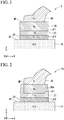
- a semiconductor device 1 includes a semiconductor layer 10, a first metal layer 21, a second metal layer 22, an electrode layer 30, and a connecting member 40.
- the semiconductor device 1 is a semiconductor device using a semiconductor substrate of silicon carbide (hereinafter occasionally referred to as SiC), such as a thyristor, a transistor, a diode, or the like.
- SiC silicon carbide
- a horizontal direction on the paper surface is defined as an X-axis direction
- a direction perpendicular to the paper surface is defined as a Y-axis direction
- a vertical direction on the paper surface is defined as a Z-axis direction.
- the semiconductor layer 10 is part of the semiconductor substrate and is composed of SiC.
- a plurality of layers e.g ., a plurality of metal layers
- the above-described plurality of layers includes a first metal layer 21, a second metal layer 22, and an electrode layer 30.
- the electrode layer 30 is one of the above-described plurality of layers and has an electrode connecting surface MF to which the conductive connecting member 40 is connected.
- the electrode layer 30 is composed of, for example, silver (hereinafter occasionally referred to as Ag) as a main component.
- the electrode layer 30 is formed outside the first metal layer 21 that will be described later.
- the outside of the first metal layer 21 refers to the side far from the semiconductor layer 10 in + (plus) direction of the thickness direction (Z-axis direction), that is, an upper side in the vertical direction on the paper surface of FIG. 1 .
- the electrode layer 30 is disposed on the outermost side among the above-described plurality of layers.
- the connecting member 40 is connected to the electrode connecting surface MF of the electrode layer 30.
- the first metal layer 21 is a layer, different from the electrode layer 30, among the above-described plurality of layers and is a metal layer disposed between the electrode layer 30 and the second metal layer 22 that will be described later.
- the first metal layer 21 is composed of, for example, titanium carbide (hereinafter occasionally referred to as TiC) as a main component. Additionally, the first metal layer 21 has a first bonding surface JF1 bonded onto the electrode layer 30 so that the electrode connecting surface MF is exposed to the outside and a second bonding surface JF2 electrically connected to the semiconductor layer 10.
- the first bonding surface JF1 is a bonding surface between the electrode layer 30 and the first metal layer 21, for example, a bonding surface formed so as to be parallel to the main surface SF and the electrode connecting surface MF of the semiconductor layer 10.
- the second bonding surface JF2 is a bonding surface between the first metal layer 21 and the second metal layer 22, for example, a bonding surface formed so as to be parallel to the main surface SF and the electrode connecting surface MF of the semiconductor layer 10.
- the first metal layer 21 has the first bonding surface JF1 on the outer side (first main surface side) and the second bonding surface JF2 on the inner side (second main surface side) that is a main surface opposite to the first main surface.
- the first metal layer 21 is electrically connected to the semiconductor layer 10 via the second bonding surface JF2 and the second metal layer 22.
- the “inner side” is the side close to the + direction of the Z-axis direction.
- the second metal layer 22 is one of the above-described plurality of layers and is a metal layer formed on the main surface SF of the semiconductor layer 10.
- the second metal layer 22 is composed of, for example, titanium (hereinafter occasionally referred to as Ti) as a main component.
- Ti titanium
- the second metal layer 22 is a layer between the first metal layer 21 and the semiconductor layer 10, is bonded onto the first metal layer 21 by the second bonding surface JF2, and is disposed in contact with the semiconductor layer 10. Additionally, the second metal layer 22 is in ohmic contact or Schottky junction with the semiconductor layer 10.
- the connecting member 40 is a conductive member that electrically connects the electrode layer 30 and the outside of the semiconductor device 1 (e.g ., a mounting substrate or a lead frame of a package), and is composed of, for example, copper (hereinafter occasionally referred to as Cu) as a main component.
- the connecting member 40 is, for example, copper wiring (copper wire) or the like.
- the second metal layer 22 of Ti, the first metal layer 21 of TiC, and the electrode layer 30 of Ag are arranged in this order from the main surface SF of the semiconductor layer 10 of SiC toward the outside (far side in the + direction of the Z-axis direction). Additionally, the connecting member 40 of Cu is connected to the electrode connecting surface MF of the electrode layer 30 and is connected to the outside of the semiconductor device 1.
- the current flowing from the outside to the semiconductor device 1 flows to the semiconductor layer 10 of SiC via the connecting member 40 of Cu, the electrode layer 30 of Ag, the first metal layer 21 of TiC, and the second metal layer 22 of Ti.
- the semiconductor device 1 includes the semiconductor layer 10, the electrode layer 30, and the first metal layer 21.
- the semiconductor layer 10 is composed of SiC (silicon carbide) and includes the plurality of layers arranged on the main surface SF side.
- the electrode layer 30 is one of the plurality of layers, has the electrode connecting surface MF to which the conductive connecting member 40 is connected, and is composed of Ag (silver) as a main component.
- the first metal layer 21 is a layer, different from the electrode layer 30, among the plurality of layers, has the first bonding surface JF1 bonded onto the electrode layer 30 so that the electrode connecting surface MF is exposed to the outside and the second bonding surface JF2 electrically connected to the semiconductor layer 10, and is composed of TiC (titanium carbide) as a main component.
- the electrode layer 30 is composed of Ag having a higher electrical conductivity than aluminum composing the conventional electrode layer, heat becomes hardly generated due to the current flowing from the electrode layer 30 to the semiconductor layer 10. Further, in the semiconductor device 1 according to the present embodiment, heat is hardly generated as described above, and since the melting point (approximately 961.8°C) of Ag of the electrode layer 30 and the melting point (approximately 3170°C) of TiC of the first metal layer 21 are higher than the melting point (about 660.3°C) of aluminum composing the conventional electrode layer 30, the current allowed to flow from the electrode layer 30 to the semiconductor layer 10 can be increased.
- the bonding strength between the electrode layer 30 and the metal layer is not lowered by a physically fragile alloy.
- the semiconductor device 1 according to the present invention can increase the allowable current without lowering the bonding strength between the electrode layer 30 and the metal layer (the first metal layer 21).
- the semiconductor device 1 since the first metal layer 21 functions as a barrier metal for preventing, for example, Cu of the connecting member 40 and Ag of the electrode layer 30 from diffusing into the semiconductor layer 10, the semiconductor device 1 according to the present invention can suppress degradation of the performance due to the diffusion of Cu and Ag.
- the semiconductor device 1 includes the second metal layer 22 composed of Ti (titanium) as a main component, which is a layer between the first metal layer 21 and the semiconductor layer 10, is bonded onto the first metal layer 21 by the second bonding surface JF2, and is in contact with the semiconductor layer 10.
- the second metal layer 22 composed of Ti (titanium) as a main component, which is a layer between the first metal layer 21 and the semiconductor layer 10, is bonded onto the first metal layer 21 by the second bonding surface JF2, and is in contact with the semiconductor layer 10.
- the second metal layer 22 of the semiconductor device 1 according to the present embodiment functions as a barrier metal, so that the semiconductor device 1 according to the present invention can further suppress the degradation of the performance due to the diffusion of Cu and Ag.
- the first metal layer 21 has the first bonding surface JF1 on the outer side (first main surface side) and the second bonding surface JF2 on the inner side (second main surface side) that is the main surface opposite to the first main surface.
- the semiconductor device 1 since the first metal layer 21 of TiC is disposed between the electrode layer 30 and the semiconductor layer 10, the semiconductor device 1 according to the present invention can increase the allowable current without lowering the bonding strength between the electrode layer 30 and the metal layer (first metal layer 21),.
- the electrode connecting surface MF of the electrode layer 30 is connected with the connecting member 40 composed of Cu (copper) as a main component.
- the melting point of Cu (approximately 1085°C) is higher than the melting point of aluminum (approximately 660.3°C)
- the current allowed to flow from the electrode layer 30 to the semiconductor layer 10 can be increased.
- Cu and Ag of the electrode layer 30 have good compatibility (connectivity) so that such a physically brittle alloy as an alloy of Ag and Ti will not be generated. Therefore, in the semiconductor device 1 according to the present embodiment, the bonding strength between the electrode layer 30 and the connecting member 40 is not lowered by a physically brittle alloy.
- the semiconductor device 1a includes the semiconductor layer 10, a first metal layer 21a, the second metal layer 22, an electrode layer 30a, and the connecting member 40.
- the same components as those in FIG. 1 are denoted by the same reference numerals, and description thereof is omitted.
- the present embodiment differs from the first embodiment in that the first metal layer 21a is disposed so as to cover surfaces, other than the electrode connecting surface MF, of the electrode layer 30a.
- the electrode layer 30a is one of a plurality of layers and has the electrode connecting surface MF to which the conductive connecting member 40 is connected, and is composed of, for example, Ag as a main component.
- the electrode layer 30a is formed such that the surfaces excluding the electrode connecting surface MF are covered with the first metal layer 21a. In other words, the electrode layer 30a is buried in the first metal layer 21a so that only the electrode connecting surface MF is exposed, and the connecting member 40 is connected to the exposed electrode connecting surface MF.
- the first metal layer 21a is a layer, different from the electrode layer 30a, among the plurality of layers, and is composed of, for example, TiC as a main component.
- the first metal layer 21a is formed so as to cover the electrode layer 30a.
- a first bonding surface JF1 is bonded onto the electrode layer 30a so as to cover the surfaces, other than the electrode connecting surface MF, of the electrode layer 30a.
- the first bonding surface JF1 includes a surface parallel to the main surface SF on the outer side (side far from the semiconductor layer 10) of the first metal layer 21a and side surfaces parallel to the thickness direction (Z-axis direction).
- first metal layer 21a is electrically connected to the semiconductor layer 10 via the second bonding surface JF2 and the second metal layer 22.
- the semiconductor device 1a includes the semiconductor layer 10, the electrode layer 30a, the first metal layer 21a, and the second metal layer 22.
- the semiconductor device 1a according to the present invention achieves the same effects as those of the first embodiment, and can increase the allowable current without lowering the bonding strength between the electrode layer 30a and the metal layer (the first metal layer 21a).
- the first metal layer 21a is bonded onto the electrode layer 30a so that the first bonding surface JF1 covers the surfaces, other than the electrode connecting surface MF, of the electrode layer 30a.
- the semiconductor device 1a since the electrode layer 30a is covered with the first metal layer 21a, the semiconductor device 1a according to the present embodiment can suppress corrosion of Ag of the electrode layer 30a, and can improve corrosion resistance.
- the semiconductor device 1a according to the present embodiment can further improve the bonding strength between the electrode layer 30a and the first metal layer 21a.
- the semiconductor device 1b includes the semiconductor layer 10, the first metal layer 21a, the electrode layer 30a, and the connecting member 40.
- the same components as those in FIG. 2 are denoted by the same reference numerals, and description thereof is omitted.
- the present embodiment differs from the second embodiment in that the semiconductor device 1b does not include the second metal layer 22.
- the second bonding surface JF2 is disposed in contact with the semiconductor layer 10.
- the first metal layer 21a is electrically connected to the semiconductor layer 10 via the second bonding surface JF2.
- the first metal layer 21a is in ohmic contact or Schottky junction with the semiconductor layer 10, in place of the second metal layer 22 of the second embodiment.
- the semiconductor device 1b includes the semiconductor layer 10, the electrode layer 30a, and the first metal layer 21a.
- the semiconductor device 1b according to the present invention achieves the same effects as those of the first embodiment and can increase the allowable current without lowering the bonding strength between the electrode layer 30a and the metal layer (the first metal layer 21a). Additionally, in the semiconductor device 1b according to the present invention, since the electrode layer 30a is covered with the first metal layer 21a, as in the second embodiment, corrosion of Ag of the electrode layer 30a can be suppressed, and corrosion resistance can be improved.
- the semiconductor device 1b according to the present invention can simplify the manufacturing process and the configuration of the metal layer.
- the semiconductor device 1c includes the semiconductor layer 10, a first metal layer 21b, a second metal layer 22a, an electrode layer 30b, and the connecting member 40.
- the same components as those in FIG. 2 are denoted by the same reference numerals, and description thereof is omitted.
- the present embodiment differs from the second embodiment in that the plurality of metal layers (the first metal layer 21b, the second metal layer 22a, and the electrode layer 30b) are arranged so as to be buried in the semiconductor layer 10.
- the second metal layer 22a is formed so as to be buried in the semiconductor layer 10, and is composed of, for example, Ti as a main component. Additionally, the second metal layer 22a is disposed inside the main surface SF of the semiconductor layer 10 on the side where the electrode layer 30b is disposed, in the thickness direction of the semiconductor layer 10. In other words, the second metal layer 22a is formed so as to have a surface aligned with the main surface SF of the semiconductor layer 10 on the side where the electrode layer 30b is disposed, in the thickness direction of the semiconductor layer 10. Further, the second metal layer 22a is disposed so as to cover surfaces, other than the surface contacting the main surface SF, of the semiconductor layer 10, along a recessed portion formed in the semiconductor layer 10.
- the second metal layer 22a is a layer between the first metal layer 21b and the semiconductor layer 10, is bonded onto the first metal layer 21b by the second bonding surface JF2, and is disposed in contact with the semiconductor layer 10. Moreover, the second metal layer 22a is in ohmic contact or Schottky junction with the semiconductor layer 10.
- the first metal layer 21b is a layer, different from the electrode layer 30b, among the plurality of layers, is formed so as to be buried in the second metal layer 22a, and is composed of, for example, TiC as a main component.
- the first metal layer 21b is formed so as to cover the electrode layer 30b and is covered with the second metal layer 22a.
- the first bonding surface JF1 of the first metal layer 21b is bonded onto the electrode layer 30b so as to cover surfaces, other than the electrode connecting surface MF, of the electrode layer 30b.
- the first bonding surface JF1 includes a surface parallel to the main surface SF, on the outer side (the side far from the semiconductor layer 10), of the first metal layer 21b and a surface parallel to the thickness direction (Z-axis direction) which is in contact with the electrode layer 30b.
- the second bonding surface JF2 includes a surface parallel to the main surface SF, on the inner side (side close to the semiconductor layer 10), of the first metal layer 21b and a surface parallel to the thickness direction (Z-axis direction) which is in contact with the second metal layer 22a.
- first metal layer 21b is electrically connected to the semiconductor layer 10 via the second bonding surface JF2 and the second metal layer 22a.
- the electrode layer 30b is one of the plurality of layers, has the electrode connecting surface MF to which the conductive connecting member 40 is connected, and is composed of, for example, Ag as a main component.
- the electrode layer 30b is formed such that the surfaces thereof excluding the electrode connecting surface MF are covered with the first metal layer 21b. In other words, the electrode layer 30b is buried in the first metal layer 21b.
- a surface opposing the electrode connecting surface MF (surface facing away from the electrode connecting surface MF) is formed inside the main surface SF of the semiconductor layer 10 on the side where the electrode layer 30b is disposed, in the thickness direction of the semiconductor layer 10. Further, the electrode layer 30b is disposed so that the electrode connecting surface MF is aligned with the main surface SF of the semiconductor layer 10 in the thickness direction.
- the semiconductor device 1c includes the semiconductor layer 10, the electrode layer 30b, the first metal layer 21b, and the second metal layer 22a.
- the semiconductor device 1c according to the present embodiment achieves the same effects as those of the second embodiment, and can increase an allowable current without lowering the bonding strength between the electrode layer 30b and the metal layer (the first metal layer 21b).
- the surface opposing the electrode connecting surface MF is disposed inside the main surface SF of the semiconductor layer 10 on the side where the electrode layer 30b is disposed, in the thickness direction of the semiconductor layer 10.
- the semiconductor device 1c since the electrode layer 30b is disposed so as to be covered with the semiconductor layer 10, the semiconductor device 1c according to the present embodiment can further suppress the corrosion of Ag of the electrode layer 30b, and further improve the corrosion resistance.
- the first metal layer 21b and the second metal layer 22a are disposed so as to cover the electrode layer 30b, and the electrode layer 30b, the first metal layer 21b, and the second metal layer 22a are buried in the semiconductor layer 10.
- the semiconductor device 1c according to the present embodiment can further improve the bonding strength among the electrode layer 30b, the first metal layer 21b, and the second metal layer 22a. Therefore, it is possible to further reduce occurrence of manufacturing troubles such as peeling of the electrode layer 30b due to, for example, a load (stress, stress) applied when the connecting member 40 is connected to the electrode layer 30b.
- the semiconductor device 1d includes the semiconductor layer 10, a first metal layer 21c, a second metal layer 22b, an electrode layer 30c, and the connecting member 40.
- the same components as those in FIG. 1 are denoted by the same reference numerals, and description thereof is omitted.
- the present embodiment differs from the first embodiment in that the shapes of the plurality of metal layers (the first metal layer 21c, the second metal layer 22b, and the electrode layer 30c) are different.
- the second metal layer 22b is a metal layer formed on the main surface SF of the semiconductor layer 10 so as to have an uneven shape, and is composed of, for example, Ti as a main component.
- a surface of the second metal layer 22b, in contact with the main surface SF of the semiconductor layer 10, is a flat surface, while a surface thereof facing the first metal layer 21c side is an uneven surface.
- FIG. 5 a case where the second metal layer 22b is formed in a mountain shape (triangular shape in cross section) is illustrated. A plurality of these mountain shapes are arranged on the semiconductor layer 10.
- the second metal layer 22b is a layer between the first metal layer 21c and the semiconductor layer 10, is bonded onto the first metal layer 21c by the second bonding surface JF2, and is disposed in contact with the semiconductor layer 10. Further, the second metal layer 22b is in ohmic contact or Schottky junction with the semiconductor layer 10.
- the second metal layers 22b having the plurality of mountain shapes may be formed so that the individual mountain shapes are separated from one another, or may be formed such that, for example, portions of the second metal layer 22b, adjacent to the plurality of mountain shapes, are integrally connected with one another.
- the first metal layer 21c is a metal layer formed along the shape of the second metal layer 22b, and is composed of, for example, TiC as a main component.
- the first metal layer 21c is disposed between the electrode layer 30c and the second metal layer 22b.
- the first bonding surface JF1 is a bonding surface between the electrode layer 30c and the first metal layer 21c
- the second bonding surface JF2 is a bonding surface between the first metal layer 21c and the second metal layer 22b.
- the first bonding surface JF1 and the second bonding surface JF2 are formed in such a shape as to follow (conform to) the uneven surface of the second metal layer 22b.
- the first metal layer 21c is configured such that the bonding area (S2) of the first bonding surface JF1 is larger than the area (S1) of the electrode connecting surface MF.
- the electrode layer 30c has the electrode connecting surface MF to which the conductive connecting member 40 is connected, and is composed of, for example, Ag as a main component.
- the electrode layer 30c is formed outside the first metal layer 21c, and the connecting member 40 is connected to the electrode connecting surface MF. Additionally, a surface, opposing the first bonding surface JF1, of the electrode layer 30c is formed so as to follow the uneven shape of the first bonding surface JF1.
- the semiconductor device 1d includes the semiconductor layer 10, the electrode layer 30c, the first metal layer 21c, and the second metal layer 22b.
- the semiconductor device 1d according to the present embodiment achieves the same effects as those of the first embodiment, and can increase an allowable current without lowering the bonding strength between the electrode layer 30c and the metal layer (the first metal layer 21c).
- the bonding area (S2) of the first bonding surface JF1 is larger than the area (S1) of the electrode connecting surface MF.
- the bonding strength between the electrode layer 30c and the first metal layer 21c can be further improved.
- the semiconductor device 1e includes the semiconductor layer 10, a first metal layer 21d, a second metal layer 22c, an electrode layer 30d, and the connecting member 40.
- the same components as those in FIG. 1 are denoted by the same reference numerals, and description thereof is omitted.
- the present embodiment differs from the first embodiment in that the shapes of the plurality of metal layers (the first metal layer 21d, the second metal layer 22c, and the electrode layer 30d) are different, and that the electrode layer 30d directly contacts the semiconductor layer 10.
- the second metal layer 22c is a metal layer including a plurality of protruding portions formed on the main surface SF of the semiconductor layer 10, and is composed of, for example, Ti as a main component.
- the protruding portions are formed in a rectangular shape in cross-sectional view (rectangular shape in cross section).
- a plurality of protruding portions are provided and formed on the semiconductor layer 10 so as to be, for example, being separated from one another.
- the second metal layer 22c is covered with the first metal layer 21d and disposed in contact with the first metal layer 21d and the semiconductor layer 10. Additionally, the second metal layer 22c is in ohmic contact or Schottky junction with the semiconductor layer 10.
- the first metal layer 21d is a metal layer formed to cover the second metal layer 22c along the shape of the second metal layer 22c, and is composed of, for example, TiC as a main component. Like the second metal layers 22c, the first metal layers 21d are formed so as to be, for example, separated from one another. The first metal layer 21d is disposed between the electrode layer 30d and the second metal layer 22c. Here, the first metal layer 21d is also in contact with the main surface SF of the semiconductor layer 10.
- first bonding surface JF1 is a bonding surface between the electrode layer 30d and the first metal layer 21d
- second bonding surface JF2 is a bonding surface between the first metal layer 21d and the second metal layer 22c.
- the first bonding surface JF1 and the second bonding surface JF2 are formed so as to follow the rectangular cross-sectional shape of the second metal layer 22c.
- the electrode layer 30d has the electrode connecting surface MF to which the conductive connecting member 40 is connected, and is composed of, for example, Ag as a main component.
- the electrode layer 30d is formed in contact with the first metal layer 21d and the semiconductor layer 10, and the connecting member 40 is connected to the electrode connecting surface MF. Additionally, a surface, opposing the first bonding surface JF1, of the electrode layer 30d is formed so as to follow the first bonding surface JF1. Further, the electrode layer 30d is in contact with the main surface SF of the semiconductor layer 10.
- the semiconductor device 1e includes the semiconductor layer 10, the electrode layer 30d, the first metal layer 21d, and the second metal layer 22c.
- the semiconductor device 1e according to the present embodiment achieves the same effects as those of the first embodiment, and can increase an allowable current without lowering the bonding strength between the electrode layer 30d and the metal layer (the first metal layer 21d).
- the semiconductor device 1f includes the semiconductor layer 10, a first metal layer 21e, a second metal layer 22d, an electrode layer 30e, and the connecting member 40.
- the same components as those in FIG. 1 are denoted by the same reference numerals, and description thereof is omitted.
- the present embodiment differs from the first embodiment in that the shapes of the plurality of metal layers (the first metal layer 21e, the second metal layer 22d, and the electrode layer 30e) are different.
- the trench shape is, for example, a rectangular shape in cross-sectional view. Additionally, the trench shape of the semiconductor layer 10 as viewed from above the main surface SF may be dotted or linear. Further, the trench shape is not limited to the rectangular shape in cross-sectional view, and may be an arbitrary shape.
- the second metal layer 22d is a metal layer formed along the plurality of trench shapes formed in the semiconductor layer 10, and is composed, for example, of Ti as a main component.
- a surface of the second metal layer 22d, bonded onto the first metal layer 21e, also has a shape corresponding to the trench shape of the semiconductor layer 10.
- the second metal layer 22d is a layer between the first metal layer 21e and the semiconductor layer 10, is bonded onto the first metal layer 21e by the second bonding surface JF2, and is disposed in contact with the semiconductor layer 10. Further, the second metal layer 22d is in ohmic contact or Schottky junction with the semiconductor layer 10.
- the first metal layer 21e is a metal layer formed along the shape of the second metal layer 22d, and is composed of, for example, TiC as a main component.
- the first metal layer 21e is disposed between the electrode layer 30e and the second metal layer 22d.
- the first bonding surface JF1 is a bonding surface between the electrode layer 30e and the first metal layer 21e
- the second bonding surface JF2 is a bonding surface between the first metal layer 21e and the second metal layer 22d.
- the first metal layer 21e is configured such that the bonding area (S2) of the first bonding surface JF1 is larger than the area (S1) of the electrode connecting surface MF.
- the electrode layer 30e has the electrode connecting surface MF to which the conductive connecting member 40 is connected, and is composed of, for example, Ag as a main component.
- the electrode layer 30e is formed outside the first metal layer 21e and in the thickness direction of the semiconductor layer 10. Apart of the electrode layer 30e is formed so as to fill the trench shape in which the first metal layer 21e is formed and so that the first metal layer 21e is not exposed.
- the connecting member 40 is connected to the electrode connecting surface MF of the electrode layer 30e.
- the semiconductor device 1f includes the semiconductor layer 10, the electrode layer 30e, the first metal layer 21e, and the second metal layer 22d.
- the semiconductor device 1f according to the present embodiment achieves the same effects as those of the first embodiment, and can increase an allowable current without lowering the bonding strength between the electrode layer 30e and the metal layer (the first metal layer 21e).
- the bonding area (S2) of the first bonding surface JF1 is larger than the area (S1) of the electrode connecting surface MF.
- the semiconductor device 1f according to the present embodiment since the area of the first bonding surface JF1 is larger (wider) than that of the first embodiment, as in the fifth embodiment, it is possible to further improve the bonding strength between the electrode layer 30e and the first metal layer 21e.
- the semiconductor device 1g according to the eighth embodiment includes the semiconductor layer 10, the first metal layer 21e, the electrode layer 30e, and the connecting member 40.
- the same components as those in FIG. 7 are denoted by the same reference numerals, and description thereof is omitted.
- the present embodiment differs from the seventh embodiment in that the semiconductor device 1g does not include the second metal layer 22d of Ti.
- the first metal layer 21e is a metal layer formed along a plurality of trench shapes formed in the semiconductor layer 10, and is composed of, for example, TiC as a main component.
- the first metal layer 21e is a layer between the electrode layer 30e and the semiconductor layer 10, is bonded onto the electrode layer 30e by the first bonding surface JF1, and is disposed in contact with the semiconductor layer 10 by the second bonding surface JF. Additionally, the first metal layer 21e is in ohmic contact or Schottky junction with the semiconductor layer 10.
- the semiconductor device 1g includes the semiconductor layer 10, the electrode layer 30e, and the first metal layer 21e.
- the semiconductor device 1g according to the present embodiment achieves the same effects as those of the seventh embodiment, and can increase an allowable current without lowering the bonding strength between the electrode layer 30e and the metal layer (the first metal layer 21e).
- the semiconductor device 1g according to the present invention can simplify the manufacturing process and the configuration of the metal layer, as compared with the seventh embodiment.
- the semiconductor device 1h according to the ninth embodiment includes the semiconductor layer 10, the first metal layer 21e, an electrode layer 30f, and the connecting member 40.
- the same components as those in FIG. 8 are denoted by the same reference numerals, and description thereof is omitted.
- the present embodiment differs from the eighth embodiment in that the shape of the electrode layer 30f is different.
- the electrode layer 30f has the electrode connecting surface MF to which the conductive connecting member 40 is connected, and is composed of, for example, Ag as a main component.
- the electrode layer 30f is formed so as to fill a plurality of trench shapes formed by the semiconductor layer 10 and the first metal layer 21e and so that a flat surface exposed to the outside of the first metal layer 21e is aligned with the electrode connecting surface MF. Additionally, the connecting member 40 is connected to the electrode connecting surface MF of the electrode layer 30f.
- the connecting member 40 is connected to the electrode connecting surface MF of the plurality of electrode layers 30f and the first metal layer 21e.
- the single connecting member 40 is connected to the electrode connecting surface MF of the plurality of electrode layers 30f.
- the semiconductor device 1h includes the semiconductor layer 10, the electrode layer 30f, and the first metal layer 21e.
- the semiconductor device 1h according to the present embodiment achieves the same effects as those of the eighth embodiment, and can increase an allowable current without lowering the bonding strength between the electrode layer 30f and the metal layer (the first metal layer 21e).
- the semiconductor device 1i includes the semiconductor layer 10, a first metal layer 21f, a second metal layer 22e, the electrode layer 30f, and the connecting member 40.
- the same components as those in FIGS. 4 and 9 are denoted by the same reference numerals, and description thereof is omitted.
- the first metal layer 21f, the second metal layer 22e, and the electrode layer 30f according to the present embodiment have the same configurations as those of the first metal layer 21b, the second metal layer 22a, and the electrode layer 30b according to the fourth embodiment, and explanation will be omitted here.
- the semiconductor device 1i includes plural sets of metal layers of the first metal layer 21f, the second metal layer 22e, and the electrode layer 30f, and each set is buried in the semiconductor layer 10 at a predetermined interval.
- the connecting member 40 is connected to the electrode connecting surface MF over the plurality of electrode layers 30f.
- the single connecting member 40 is connected to the electrode connecting surface MF of the plurality of electrode layers 30f.
- the semiconductor device 1i includes the plural sets of metal layers of the semiconductor layer 10, the electrode layer 30f, the first metal layer 21f, and the second metal layer 22e.
- the semiconductor device 1i according to the present embodiment achieves the same effects as those of the fourth embodiment, and can increase an allowable current without lowering the bonding strength between the electrode layer 30f and the metal layer (the first metal layer 21f).
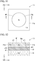
- the semiconductor device 1j shown in FIG. 12 shows a cross section along a line AB of the semiconductor device 1j shown in FIG. 11 . Additionally, in FIGS. 11 and 12 , to simplify the description, the description of the connecting member 40 is omitted.
- FIGS. 11 and 12 the same components as those in FIG. 1 are denoted by the same reference numerals, and the description thereof will be omitted.
- the semiconductor device 1j includes a columnar electrode layer 30g and a first metal layer 21g disposed so as to cover a side surface (circumferential surface) of the electrode layer 30g, on the main surface SF side of the semiconductor layer 10 including the electrode layer 30g.
- the semiconductor device 1j includes the semiconductor layer 10, the first metal layer 21g, the second metal layer 22, and the electrode layer 30g.
- the electrode layer 30g has the electrode connecting surface MF to which the conductive connecting member 40 is connected, and is composed of, for example, Ag as a main component.
- the electrode layer 30g is formed in a circular shape on a plane (XY-plane) parallel to the main surface SF, and is surrounded by the first metal layer 21g. Additionally, the connecting member 40 is connected to the electrode connecting surface MF of the electrode layer 30g.
- the first metal layer 21g is disposed around the electrode layer 30g on the XY-plane, and is composed, for example, of TiC as a main component. Additionally, the first metal layer 21g has a first bonding surface JF1 bonded onto the peripheral surface (side surface) of the electrode layer 30g so that the electrode connecting surface MF is exposed to the outside and a second bonding surface JF2 bonded onto the second metal layer 22. The second bonding surface JF2 of the first metal layer 21g is electrically connected to the semiconductor layer 10 via the second metal layer 22.
- the first bonding surface JF1 is a bonding surface between the electrode layer 30g and the first metal layer 21g, for example, a bonding surface formed so as to be perpendicular to the main surface SF and the electrode connecting surface MF of the semiconductor layer 10.
- the first bonding surface JF1 is a bonding surface parallel to the thickness direction (Z-axis direction) of the semiconductor device 1j.
- the second bonding surface JF2 is a bonding surface between the first metal layer 21g and the second metal layer 22, for example, is a bonding surface formed so as to be parallel to the main surface SF and the electrode connecting surface MF of the semiconductor layer 10.
- the second metal layer 22 is disposed between the semiconductor layer 10 and the first metal layer 21g and electrode layer 30g. Additionally, the second metal layer 22 is disposed in contact with surfaces of the electrode layer 30g and the first metal layer 21g which face away from the main surface SF of the semiconductor layer 10.
- the semiconductor device 1j includes the semiconductor layer 10, the electrode layer 30g, the first metal layer 21g, and the second metal layer 22.
- the semiconductor device 1j according to the present embodiment achieves the same effects as those of the first embodiment, and can increase an allowable current without lowering the bonding strength between the electrode layer 30g and the metal layer (the first metal layer 21g and the second metal layer 22).
- the semiconductor device 1k includes: an electrode layer 30h including a columnar electrode layer 30h-1 and a columnar electrode layer 30h-2 disposed concentric to the electrode layer 30h-1; and a first metal layer (21g, 21h) disposed so as to cover the electrode layer 30h, on the main surface SF side of the semiconductor layer 10 including the electrode layer 30h.
- the semiconductor device 1k shown in FIG. 14 shows a cross section along a line AB of the semiconductor device 1k shown in FIG. 13 . Additionally, in FIGS. 13 and 14 , to simplify the description, the description of the connecting member 40 is omitted.
- FIGS. 13 and 14 the same components as those in FIGS. 11 and 12 are denoted by the same reference numerals, and description thereof is omitted.
- the semiconductor device 1k according to the present embodiment is a modified example where the electrode layer 30h is divided into the electrode layer 30h-1 and the electrode layer 30h-2, and the first metal layer 21h is added to the above-described twelfth embodiment.
- the semiconductor device 1k includes the semiconductor layer 10, the first metal layer (21g, 21h), the second metal layer 22, and the electrode layer 30h.
- the first metal layer 21h is a columnar metal layer disposed between an outer periphery of the electrode layer 30h-1 and an inner periphery of the electrode layer 30h-2 on a plane (XY-plane) parallel to the main plane SF, and is composed of, for example, TiC as a main component. Additionally, the first metal layer 21g and the first metal layer 21h have a first bonding surface JF1 bonded onto the electrode layer 30h so that the electrode connecting surface MF is exposed to the outside and a second bonding surface JF2 bonded onto the second metal layer 22.
- the first bonding surface JF1 is a bonding surface between the electrode layer 30h (30h-1, 30h-2) and the first metal layer (21g, 21h), for example, a bonding surface formed so as to be perpendicular to the main surface SF and the electrode connecting surface MF of the semiconductor layer 10.
- the first bonding surface JF1 is a bonding surface parallel to the thickness direction (Z-axis direction) of the semiconductor device 1k.
- the second bonding surface JF2 is a bonding surface between the first metal layer (21g, 21h) and the second metal layer 22, for example, a bonding surface formed parallel to the main surface SF and the electrode connecting surface MF of the semiconductor layer 10.
- the electrode layer 30h includes the above-described columnar electrode layer 30h-1 and the columnar electrode layer 30h-2.
- the columnar electrode layer 30h-2 is disposed outside in the radial direction of, and separated from, the electrode layer 30h-1.
- the electrode layer 30h (the electrode layers 30h-1, 30h-2) is disposed such that the periphery thereof is surrounded by the first metal layers (21g, 21h).
- the connecting member 40 is connected to the electrode connecting surface MF of the electrode layer 30h (the electrode layers 30h-1 and 30h-2).
- the semiconductor device 1k includes the semiconductor layer 10, the electrode layer 30h (the electrode layers 30h-1, 30h-2), the first metal layer (21g, 21h), and the second metal layer 22.
- the semiconductor device 1k according to the present embodiment achieves the same effects as those of the eleventh embodiment, and can increase an allowable current without lowering the bonding strength between the electrode layer 30h (the electrode layers 30h-1 and 30h-2) and the metal layer (the first metal layer (21g, 21h) and the second metal layer 22).
- the present invention is not limited to the above embodiments, but can be modified within a scope, not departing from the gist, of the present invention.
- the connecting member 40 connected to the electrode layer 30 (30a to 30h) is Cu (copper)
- the present invention is not limited thereto, and the connecting member 40 may be gold (Au), aluminum (Al), or another metal.
Landscapes
- Electrodes Of Semiconductors (AREA)
- Internal Circuitry In Semiconductor Integrated Circuit Devices (AREA)
- Wire Bonding (AREA)
Abstract
Description
- The present invention relates to a semiconductor device.
- Recently, a semiconductor device in which silicon carbide (SiC) is used as a semiconductor layer is widely used because it has a wide band gap and can operate at high temperature. In a conventional semiconductor device using silicon carbide, a metal layer is bonded over a semiconductor layer of silicon carbide, and an electrode layer is bonded over the metal layer. The metal layer is composed of, for example, titanium (Ti) as a main component, and the electrode layer is composed of, for example, aluminum (Al) as a main component.
- Generally, a semiconductor device generates heat according to a flowing current. Additionally, in the case of the above-described conventional semiconductor device, since a melting point of aluminum of the electrode layer is the lowest among the respective layers, an allowable current that can flow from the electrode layer to the semiconductor layer is limited to a current value that is lower than the temperature at which the electrode layer composed of aluminum melts. Therefore, in the conventional semiconductor device, in order to increase such an allowable current, in place of aluminum, an electrode layer is composed of silver (Ag) having a melting point higher than that of aluminum (see, for example, Patent Document 1).
- [Patent Literature 1] Japanese Patent Application Laid-Open Publication No.
2013-125922 - However, in the above-described conventional semiconductor device, if an electrode layer is composed of silver instead of aluminum, titanium is used for the metal layer bonded onto this electrode layer, so that an alloy of silver and titanium will be generated. The alloys of silver and titanium generally have low strength and are known as physically brittle alloys. In the conventional semiconductor device, the bonding strength between the electrode layer and the metal layer occasionally decreases due to generation of a physically brittle alloy of silver and titanium. Therefore, in the conventional semiconductor device, it has been difficult to increase the allowable current without lowering the bonding strength between the electrode layer and the metal layer.
- The present invention has been made in view of the above problems and an object thereof is to provide a semiconductor device capable of increasing an allowable current without lowering a bonding strength between an electrode layer and a metal layer.
- In order to solve the above problem, a semiconductor device according to one aspect of the present invention includes: a semiconductor layer of silicon carbide including a plurality of layers disposed on a main surface side; an electrode layer that is one of the plurality of layers, wherein the electrode layer has an electrode connecting surface to which a conductive connecting member is connected, and the electrode layer is composed mainly of silver; and a first metal layer that is a layer, different from the electrode layer, among the plurality of layers, wherein the first metal layer has a first bonding surface bonded onto the electrode layer such that the electrode connecting surface is exposed to an outside, and a second bonding surface electrically connected to the semiconductor layer, and the first metal layer is composed mainly of titanium carbide.
- Additionally, the semiconductor device according to one aspect of the present invention may further includes: a second metal layer between the first metal layer and the semiconductor layer, wherein the second metal layer is bonded onto the first metal layer by the second bonding surface, the second metal layer is disposed in contact with the semiconductor layer, and the second metal layer is composed mainly of titanium.
- Further, in the semiconductor device according to one aspect of the present invention, the first metal layer may have the first bonding surface on the first main surface side and the second bonding surface on a second main surface side opposite to the first main surface.
- Moreover, in the semiconductor device according to one aspect of the present invention, the first metal layer may be bonded onto the electrode layer so that the first bonding surface covers a surface, other than the electrode connecting surface, of the electrode layer.
- Additionally, in the semiconductor device according to one aspect of the present invention, in the first metal layer, a bonding area of the first bonding surface may be larger than an area of the electrode connecting surface.
- Further, in the semiconductor device according to one aspect of the present invention, a surface, opposing the electrode connecting surface, of the electrode layer may be disposed inside the main surface of the semiconductor layer on the side where the electrode layer is disposed, in a thickness direction of the semiconductor layer.
- Moreover, in the semiconductor device according to one aspect of the present invention, the connecting member composed mainly of copper may be connected to the electrode connecting surface of the electrode layer.
- According to the present invention, the electrode layer having the electrode connecting surface to which the conductive connecting member is connected is composed mainly of silver. Additionally, the first metal layer has the first bonding surface bonded to the electrode layer so that the electrode connecting surface is exposed to the outside, and the second bonding surface electrically connected to the semiconductor layer, and is composed mainly of titanium carbide. Since the electrode layer is composed of silver having the higher electrical conductivity than aluminum composing the conventional electrode layer, heat is hardly generated by a current flowing from the electrode layer to the semiconductor layer. Further, since heat is hardly generated in this way, the melting points of silver of the electrode layer and titanium carbide of the first metal layer are higher than the melting point of aluminum composing the conventional electrode layer, the allowable current can be increased. Additionally, since a physically brittle alloy such as an alloy of silver and titanium is not generated between the first metal layer of titanium carbide and silver of the electrode layer, the bonding strength between the electrode layer and the metal layer is not lowered by a physically brittle alloy. Therefore, the semiconductor device according to the present invention can increase the allowable current without lowering the bonding strength between the electrode layer and the metal layer.
-
-
FIG. 1 is a sectional configuration diagram showing an example of a semiconductor device according to a first embodiment. -
FIG. 2 is a sectional configuration diagram showing an example of a semiconductor device according to a second embodiment. -
FIG. 3 is a sectional configuration diagram showing an example of a semiconductor device according to a third embodiment. -
FIG. 4 is a sectional configuration diagram showing an example of a semiconductor device according to a fourth embodiment. -
FIG. 5 is a sectional configuration diagram showing an example of a semiconductor device according to a fifth embodiment. -
FIG. 6 is a sectional configuration diagram showing an example of a semiconductor device according to a sixth embodiment. -
FIG. 7 is a sectional configuration diagram showing an example of a semiconductor device according to a seventh embodiment. -
FIG. 8 is a sectional configuration diagram showing an example of a semiconductor device according to an eighth embodiment. -
FIG. 9 is a sectional configuration diagram showing an example of a semiconductor device according to a ninth embodiment. -
FIG. 10 is a sectional configuration diagram showing an example of a semiconductor device according to a tenth embodiment. -
FIG. 11 is a main-surface-side plan configuration diagram showing an example of a semiconductor device according to an eleventh embodiment. -
FIG. 12 is a sectional configuration diagram showing an example of a semiconductor device according to the eleventh embodiment. -
FIG. 13 is a main-surface-side plan configuration diagram showing an example of a semiconductor device according to a twelfth embodiment. -
FIG. 14 is a sectional configuration diagram showing an example of a semiconductor device according to the twelfth embodiment. - Hereinafter, semiconductor devices according to embodiments of the present invention will be described with reference to the drawings.
- As shown in
FIG. 1 , asemiconductor device 1 according to the first embodiment includes asemiconductor layer 10, afirst metal layer 21, asecond metal layer 22, anelectrode layer 30, and a connectingmember 40. Thesemiconductor device 1 is a semiconductor device using a semiconductor substrate of silicon carbide (hereinafter occasionally referred to as SiC), such as a thyristor, a transistor, a diode, or the like. - Here, in
FIG. 1 , a horizontal direction on the paper surface is defined as an X-axis direction, a direction perpendicular to the paper surface is defined as a Y-axis direction, and a vertical direction on the paper surface (thickness direction of the semiconductor layer 10) is defined as a Z-axis direction. - The
semiconductor layer 10 is part of the semiconductor substrate and is composed of SiC. In thesemiconductor layer 10, a plurality of layers (e.g., a plurality of metal layers) are arranged on a main surface SF side. - Here, the above-described plurality of layers includes a
first metal layer 21, asecond metal layer 22, and anelectrode layer 30. - The
electrode layer 30 is one of the above-described plurality of layers and has an electrode connecting surface MF to which the conductive connectingmember 40 is connected. Theelectrode layer 30 is composed of, for example, silver (hereinafter occasionally referred to as Ag) as a main component. Theelectrode layer 30 is formed outside thefirst metal layer 21 that will be described later. Here, the outside of thefirst metal layer 21 refers to the side far from thesemiconductor layer 10 in + (plus) direction of the thickness direction (Z-axis direction), that is, an upper side in the vertical direction on the paper surface ofFIG. 1 . Theelectrode layer 30 is disposed on the outermost side among the above-described plurality of layers. The connectingmember 40 is connected to the electrode connecting surface MF of theelectrode layer 30. - The
first metal layer 21 is a layer, different from theelectrode layer 30, among the above-described plurality of layers and is a metal layer disposed between theelectrode layer 30 and thesecond metal layer 22 that will be described later. Thefirst metal layer 21 is composed of, for example, titanium carbide (hereinafter occasionally referred to as TiC) as a main component. Additionally, thefirst metal layer 21 has a first bonding surface JF1 bonded onto theelectrode layer 30 so that the electrode connecting surface MF is exposed to the outside and a second bonding surface JF2 electrically connected to thesemiconductor layer 10. - Here, the first bonding surface JF1 is a bonding surface between the
electrode layer 30 and thefirst metal layer 21, for example, a bonding surface formed so as to be parallel to the main surface SF and the electrode connecting surface MF of thesemiconductor layer 10. Additionally, the second bonding surface JF2 is a bonding surface between thefirst metal layer 21 and thesecond metal layer 22, for example, a bonding surface formed so as to be parallel to the main surface SF and the electrode connecting surface MF of thesemiconductor layer 10. - The
first metal layer 21 has the first bonding surface JF1 on the outer side (first main surface side) and the second bonding surface JF2 on the inner side (second main surface side) that is a main surface opposite to the first main surface. Here, in the present embodiment, thefirst metal layer 21 is electrically connected to thesemiconductor layer 10 via the second bonding surface JF2 and thesecond metal layer 22. Here, the "inner side" is the side close to the + direction of the Z-axis direction. - The
second metal layer 22 is one of the above-described plurality of layers and is a metal layer formed on the main surface SF of thesemiconductor layer 10. Thesecond metal layer 22 is composed of, for example, titanium (hereinafter occasionally referred to as Ti) as a main component. Thesecond metal layer 22 is a layer between thefirst metal layer 21 and thesemiconductor layer 10, is bonded onto thefirst metal layer 21 by the second bonding surface JF2, and is disposed in contact with thesemiconductor layer 10. Additionally, thesecond metal layer 22 is in ohmic contact or Schottky junction with thesemiconductor layer 10. - The connecting
member 40 is a conductive member that electrically connects theelectrode layer 30 and the outside of the semiconductor device 1 (e.g., a mounting substrate or a lead frame of a package), and is composed of, for example, copper (hereinafter occasionally referred to as Cu) as a main component. The connectingmember 40 is, for example, copper wiring (copper wire) or the like. - As described above, in the
semiconductor device 1 according to the present embodiment, thesecond metal layer 22 of Ti, thefirst metal layer 21 of TiC, and theelectrode layer 30 of Ag are arranged in this order from the main surface SF of thesemiconductor layer 10 of SiC toward the outside (far side in the + direction of the Z-axis direction). Additionally, the connectingmember 40 of Cu is connected to the electrode connecting surface MF of theelectrode layer 30 and is connected to the outside of thesemiconductor device 1. - Further, the current flowing from the outside to the
semiconductor device 1 flows to thesemiconductor layer 10 of SiC via the connectingmember 40 of Cu, theelectrode layer 30 of Ag, thefirst metal layer 21 of TiC, and thesecond metal layer 22 of Ti. - As described above, the
semiconductor device 1 according to the present embodiment includes thesemiconductor layer 10, theelectrode layer 30, and thefirst metal layer 21. Thesemiconductor layer 10 is composed of SiC (silicon carbide) and includes the plurality of layers arranged on the main surface SF side. Theelectrode layer 30 is one of the plurality of layers, has the electrode connecting surface MF to which the conductive connectingmember 40 is connected, and is composed of Ag (silver) as a main component. Thefirst metal layer 21 is a layer, different from theelectrode layer 30, among the plurality of layers, has the first bonding surface JF1 bonded onto theelectrode layer 30 so that the electrode connecting surface MF is exposed to the outside and the second bonding surface JF2 electrically connected to thesemiconductor layer 10, and is composed of TiC (titanium carbide) as a main component. - Thus, in the
semiconductor device 1 according to the present embodiment, since theelectrode layer 30 is composed of Ag having a higher electrical conductivity than aluminum composing the conventional electrode layer, heat becomes hardly generated due to the current flowing from theelectrode layer 30 to thesemiconductor layer 10. Further, in thesemiconductor device 1 according to the present embodiment, heat is hardly generated as described above, and since the melting point (approximately 961.8°C) of Ag of theelectrode layer 30 and the melting point (approximately 3170°C) of TiC of thefirst metal layer 21 are higher than the melting point (about 660.3°C) of aluminum composing theconventional electrode layer 30, the current allowed to flow from theelectrode layer 30 to thesemiconductor layer 10 can be increased. - Moreover, since a physically brittle alloy such as an alloy of Ag and Ti is not formed between the
first metal layer 21 of TiC and theelectrode layer 30 of Ag. Therefore, in thesemiconductor device 1 according to the present embodiment, the bonding strength between theelectrode layer 30 and the metal layer (e.g., the first metal layer 21) is not lowered by a physically fragile alloy. In thesemiconductor device 1 according to the present embodiment, it is possible to reduce an occurrence of manufacturing troubles such that theelectrode layer 30 and the metal layer (e.g., the first metal layer 21) are peeled off due to, for example, a load (stress, stress) applied when the connectingmember 40 is connected to theelectrode layer 30. - Therefore, the
semiconductor device 1 according to the present invention can increase the allowable current without lowering the bonding strength between theelectrode layer 30 and the metal layer (the first metal layer 21). - Additionally, since the
first metal layer 21 functions as a barrier metal for preventing, for example, Cu of the connectingmember 40 and Ag of theelectrode layer 30 from diffusing into thesemiconductor layer 10, thesemiconductor device 1 according to the present invention can suppress degradation of the performance due to the diffusion of Cu and Ag. - Further, the
semiconductor device 1 according to the present embodiment includes thesecond metal layer 22 composed of Ti (titanium) as a main component, which is a layer between thefirst metal layer 21 and thesemiconductor layer 10, is bonded onto thefirst metal layer 21 by the second bonding surface JF2, and is in contact with thesemiconductor layer 10. - As a result, like the
first metal layer 21, thesecond metal layer 22 of thesemiconductor device 1 according to the present embodiment functions as a barrier metal, so that thesemiconductor device 1 according to the present invention can further suppress the degradation of the performance due to the diffusion of Cu and Ag. - Moreover, in the present embodiment, the
first metal layer 21 has the first bonding surface JF1 on the outer side (first main surface side) and the second bonding surface JF2 on the inner side (second main surface side) that is the main surface opposite to the first main surface. - Accordingly, since the
first metal layer 21 of TiC is disposed between theelectrode layer 30 and thesemiconductor layer 10, thesemiconductor device 1 according to the present invention can increase the allowable current without lowering the bonding strength between theelectrode layer 30 and the metal layer (first metal layer 21),. - Additionally, in the present embodiment, the electrode connecting surface MF of the
electrode layer 30 is connected with the connectingmember 40 composed of Cu (copper) as a main component. - Accordingly, since the melting point of Cu (approximately 1085°C) is higher than the melting point of aluminum (approximately 660.3°C), the current allowed to flow from the
electrode layer 30 to thesemiconductor layer 10 can be increased. Further, Cu and Ag of theelectrode layer 30 have good compatibility (connectivity) so that such a physically brittle alloy as an alloy of Ag and Ti will not be generated. Therefore, in thesemiconductor device 1 according to the present embodiment, the bonding strength between theelectrode layer 30 and the connectingmember 40 is not lowered by a physically brittle alloy. - Next, a
semiconductor device 1a according to a second embodiment of the present invention will be described with reference toFIG. 2 . - As shown in
FIG. 2 , thesemiconductor device 1a according to the second embodiment includes thesemiconductor layer 10, afirst metal layer 21a, thesecond metal layer 22, anelectrode layer 30a, and the connectingmember 40. Here, inFIG. 2 , the same components as those inFIG. 1 are denoted by the same reference numerals, and description thereof is omitted. - The present embodiment differs from the first embodiment in that the
first metal layer 21a is disposed so as to cover surfaces, other than the electrode connecting surface MF, of theelectrode layer 30a. - The
electrode layer 30a is one of a plurality of layers and has the electrode connecting surface MF to which the conductive connectingmember 40 is connected, and is composed of, for example, Ag as a main component. Theelectrode layer 30a is formed such that the surfaces excluding the electrode connecting surface MF are covered with thefirst metal layer 21a. In other words, theelectrode layer 30a is buried in thefirst metal layer 21a so that only the electrode connecting surface MF is exposed, and the connectingmember 40 is connected to the exposed electrode connecting surface MF. - The
first metal layer 21a is a layer, different from theelectrode layer 30a, among the plurality of layers, and is composed of, for example, TiC as a main component. Thefirst metal layer 21a is formed so as to cover theelectrode layer 30a. For example, in thefirst metal layer 21a, a first bonding surface JF1 is bonded onto theelectrode layer 30a so as to cover the surfaces, other than the electrode connecting surface MF, of theelectrode layer 30a. - Here, the first bonding surface JF1 includes a surface parallel to the main surface SF on the outer side (side far from the semiconductor layer 10) of the
first metal layer 21a and side surfaces parallel to the thickness direction (Z-axis direction). - Additionally, the
first metal layer 21a is electrically connected to thesemiconductor layer 10 via the second bonding surface JF2 and thesecond metal layer 22. - As described above, the
semiconductor device 1a according to the present embodiment includes thesemiconductor layer 10, theelectrode layer 30a, thefirst metal layer 21a, and thesecond metal layer 22. - As a result, the
semiconductor device 1a according to the present invention achieves the same effects as those of the first embodiment, and can increase the allowable current without lowering the bonding strength between theelectrode layer 30a and the metal layer (thefirst metal layer 21a). - Additionally, in the present embodiment, the
first metal layer 21a is bonded onto theelectrode layer 30a so that the first bonding surface JF1 covers the surfaces, other than the electrode connecting surface MF, of theelectrode layer 30a. - As a result, since the
electrode layer 30a is covered with thefirst metal layer 21a, thesemiconductor device 1a according to the present embodiment can suppress corrosion of Ag of theelectrode layer 30a, and can improve corrosion resistance. - Further, since the area of the first bonding surface JF1 is larger than that of the first embodiment, the
semiconductor device 1a according to the present embodiment can further improve the bonding strength between theelectrode layer 30a and thefirst metal layer 21a. - Next, a
semiconductor device 1b according to a third embodiment of the present invention will be described with reference toFIG. 3 . - As shown in
FIG. 3 , thesemiconductor device 1b according to the third embodiment includes thesemiconductor layer 10, thefirst metal layer 21a, theelectrode layer 30a, and the connectingmember 40. Here, inFIG. 3 , the same components as those inFIG. 2 are denoted by the same reference numerals, and description thereof is omitted. - The present embodiment differs from the second embodiment in that the
semiconductor device 1b does not include thesecond metal layer 22. - In the
first metal layer 21a, the second bonding surface JF2 is disposed in contact with thesemiconductor layer 10. In other words, thefirst metal layer 21a is electrically connected to thesemiconductor layer 10 via the second bonding surface JF2. Additionally, thefirst metal layer 21a is in ohmic contact or Schottky junction with thesemiconductor layer 10, in place of thesecond metal layer 22 of the second embodiment. Here, since other configurations of the present embodiment are similar to those of the second embodiment, description thereof will be omitted here. - As described above, the
semiconductor device 1b according to the present embodiment includes thesemiconductor layer 10, theelectrode layer 30a, and thefirst metal layer 21a. - As a result, the
semiconductor device 1b according to the present invention achieves the same effects as those of the first embodiment and can increase the allowable current without lowering the bonding strength between theelectrode layer 30a and the metal layer (thefirst metal layer 21a). Additionally, in thesemiconductor device 1b according to the present invention, since theelectrode layer 30a is covered with thefirst metal layer 21a, as in the second embodiment, corrosion of Ag of theelectrode layer 30a can be suppressed, and corrosion resistance can be improved. - Further, since there is no need to form the
second metal layer 22, thesemiconductor device 1b according to the present invention can simplify the manufacturing process and the configuration of the metal layer. - Next, a
semiconductor device 1c according to a fourth embodiment of the present invention will be described with reference toFIG. 4 . - As shown in
FIG. 4 , thesemiconductor device 1c according to the fourth embodiment includes thesemiconductor layer 10, afirst metal layer 21b, asecond metal layer 22a, anelectrode layer 30b, and the connectingmember 40. Here, inFIG. 4 , the same components as those inFIG. 2 are denoted by the same reference numerals, and description thereof is omitted. - The present embodiment differs from the second embodiment in that the plurality of metal layers (the
first metal layer 21b, thesecond metal layer 22a, and theelectrode layer 30b) are arranged so as to be buried in thesemiconductor layer 10. - The
second metal layer 22a is formed so as to be buried in thesemiconductor layer 10, and is composed of, for example, Ti as a main component. Additionally, thesecond metal layer 22a is disposed inside the main surface SF of thesemiconductor layer 10 on the side where theelectrode layer 30b is disposed, in the thickness direction of thesemiconductor layer 10. In other words, thesecond metal layer 22a is formed so as to have a surface aligned with the main surface SF of thesemiconductor layer 10 on the side where theelectrode layer 30b is disposed, in the thickness direction of thesemiconductor layer 10. Further, thesecond metal layer 22a is disposed so as to cover surfaces, other than the surface contacting the main surface SF, of thesemiconductor layer 10, along a recessed portion formed in thesemiconductor layer 10. Thesecond metal layer 22a is a layer between thefirst metal layer 21b and thesemiconductor layer 10, is bonded onto thefirst metal layer 21b by the second bonding surface JF2, and is disposed in contact with thesemiconductor layer 10. Moreover, thesecond metal layer 22a is in ohmic contact or Schottky junction with thesemiconductor layer 10. - The
first metal layer 21b is a layer, different from theelectrode layer 30b, among the plurality of layers, is formed so as to be buried in thesecond metal layer 22a, and is composed of, for example, TiC as a main component. Thefirst metal layer 21b is formed so as to cover theelectrode layer 30b and is covered with thesecond metal layer 22a. For example, the first bonding surface JF1 of thefirst metal layer 21b is bonded onto theelectrode layer 30b so as to cover surfaces, other than the electrode connecting surface MF, of theelectrode layer 30b. - Here, the first bonding surface JF1 includes a surface parallel to the main surface SF, on the outer side (the side far from the semiconductor layer 10), of the
first metal layer 21b and a surface parallel to the thickness direction (Z-axis direction) which is in contact with theelectrode layer 30b. Additionally, the second bonding surface JF2 includes a surface parallel to the main surface SF, on the inner side (side close to the semiconductor layer 10), of thefirst metal layer 21b and a surface parallel to the thickness direction (Z-axis direction) which is in contact with thesecond metal layer 22a. - Further, the
first metal layer 21b is electrically connected to thesemiconductor layer 10 via the second bonding surface JF2 and thesecond metal layer 22a. - The
electrode layer 30b is one of the plurality of layers, has the electrode connecting surface MF to which the conductive connectingmember 40 is connected, and is composed of, for example, Ag as a main component. Theelectrode layer 30b is formed such that the surfaces thereof excluding the electrode connecting surface MF are covered with thefirst metal layer 21b. In other words, theelectrode layer 30b is buried in thefirst metal layer 21b. Additionally, in theelectrode layer 30b, a surface opposing the electrode connecting surface MF (surface facing away from the electrode connecting surface MF) is formed inside the main surface SF of thesemiconductor layer 10 on the side where theelectrode layer 30b is disposed, in the thickness direction of thesemiconductor layer 10. Further, theelectrode layer 30b is disposed so that the electrode connecting surface MF is aligned with the main surface SF of thesemiconductor layer 10 in the thickness direction. - As described above, the
semiconductor device 1c according to the present embodiment includes thesemiconductor layer 10, theelectrode layer 30b, thefirst metal layer 21b, and thesecond metal layer 22a. - As a result, the
semiconductor device 1c according to the present embodiment achieves the same effects as those of the second embodiment, and can increase an allowable current without lowering the bonding strength between theelectrode layer 30b and the metal layer (thefirst metal layer 21b). - Further, in the present embodiment, in the
electrode layer 30b, the surface opposing the electrode connecting surface MF is disposed inside the main surface SF of thesemiconductor layer 10 on the side where theelectrode layer 30b is disposed, in the thickness direction of thesemiconductor layer 10. - Thus, since the
electrode layer 30b is disposed so as to be covered with thesemiconductor layer 10, thesemiconductor device 1c according to the present embodiment can further suppress the corrosion of Ag of theelectrode layer 30b, and further improve the corrosion resistance. - Moreover, in the
semiconductor device 1c according to the present embodiment, thefirst metal layer 21b and thesecond metal layer 22a are disposed so as to cover theelectrode layer 30b, and theelectrode layer 30b, thefirst metal layer 21b, and thesecond metal layer 22a are buried in thesemiconductor layer 10. - As a result, the
semiconductor device 1c according to the present embodiment can further improve the bonding strength among theelectrode layer 30b, thefirst metal layer 21b, and thesecond metal layer 22a. Therefore, it is possible to further reduce occurrence of manufacturing troubles such as peeling of theelectrode layer 30b due to, for example, a load (stress, stress) applied when the connectingmember 40 is connected to theelectrode layer 30b. - Next, a
semiconductor device 1d according to a fifth embodiment of the present invention will be described with reference toFIG. 5 . - As shown in
FIG. 5 , thesemiconductor device 1d according to the fifth embodiment includes thesemiconductor layer 10, afirst metal layer 21c, asecond metal layer 22b, anelectrode layer 30c, and the connectingmember 40. Here, inFIG. 5 , the same components as those inFIG. 1 are denoted by the same reference numerals, and description thereof is omitted. - The present embodiment differs from the first embodiment in that the shapes of the plurality of metal layers (the
first metal layer 21c, thesecond metal layer 22b, and theelectrode layer 30c) are different. - The
second metal layer 22b is a metal layer formed on the main surface SF of thesemiconductor layer 10 so as to have an uneven shape, and is composed of, for example, Ti as a main component. A surface of thesecond metal layer 22b, in contact with the main surface SF of thesemiconductor layer 10, is a flat surface, while a surface thereof facing thefirst metal layer 21c side is an uneven surface. - Additionally, in
FIG. 5 , a case where thesecond metal layer 22b is formed in a mountain shape (triangular shape in cross section) is illustrated. A plurality of these mountain shapes are arranged on thesemiconductor layer 10. Thesecond metal layer 22b is a layer between thefirst metal layer 21c and thesemiconductor layer 10, is bonded onto thefirst metal layer 21c by the second bonding surface JF2, and is disposed in contact with thesemiconductor layer 10. Further, thesecond metal layer 22b is in ohmic contact or Schottky junction with thesemiconductor layer 10. - Here, as shown in
FIG. 5 , the second metal layers 22b having the plurality of mountain shapes may be formed so that the individual mountain shapes are separated from one another, or may be formed such that, for example, portions of thesecond metal layer 22b, adjacent to the plurality of mountain shapes, are integrally connected with one another. - The
first metal layer 21c is a metal layer formed along the shape of thesecond metal layer 22b, and is composed of, for example, TiC as a main component. Thefirst metal layer 21c is disposed between theelectrode layer 30c and thesecond metal layer 22b. - Here, the first bonding surface JF1 is a bonding surface between the
electrode layer 30c and thefirst metal layer 21c, while the second bonding surface JF2 is a bonding surface between thefirst metal layer 21c and thesecond metal layer 22b. The first bonding surface JF1 and the second bonding surface JF2 are formed in such a shape as to follow (conform to) the uneven surface of thesecond metal layer 22b. Additionally, thefirst metal layer 21c is configured such that the bonding area (S2) of the first bonding surface JF1 is larger than the area (S1) of the electrode connecting surface MF. - The
electrode layer 30c has the electrode connecting surface MF to which the conductive connectingmember 40 is connected, and is composed of, for example, Ag as a main component. Theelectrode layer 30c is formed outside thefirst metal layer 21c, and the connectingmember 40 is connected to the electrode connecting surface MF. Additionally, a surface, opposing the first bonding surface JF1, of theelectrode layer 30c is formed so as to follow the uneven shape of the first bonding surface JF1. - As described above, the
semiconductor device 1d according to the present embodiment includes thesemiconductor layer 10, theelectrode layer 30c, thefirst metal layer 21c, and thesecond metal layer 22b. - As a result, the
semiconductor device 1d according to the present embodiment achieves the same effects as those of the first embodiment, and can increase an allowable current without lowering the bonding strength between theelectrode layer 30c and the metal layer (thefirst metal layer 21c). - Additionally, in the present embodiment, in the
first metal layer 21c, the bonding area (S2) of the first bonding surface JF1 is larger than the area (S1) of the electrode connecting surface MF. - Thus, in the
semiconductor device 1d according to the present embodiment, since the area of the first bonding surface JF1 is larger (wider) than that of the first embodiment, the bonding strength between theelectrode layer 30c and thefirst metal layer 21c can be further improved. - Next, a
semiconductor device 1e according to a sixth embodiment of the present invention will be described with reference toFIG. 6 . - As shown in
FIG. 6 , thesemiconductor device 1e according to the sixth embodiment includes thesemiconductor layer 10, afirst metal layer 21d, asecond metal layer 22c, anelectrode layer 30d, and the connectingmember 40. Here, inFIG. 6 , the same components as those inFIG. 1 are denoted by the same reference numerals, and description thereof is omitted. - The present embodiment differs from the first embodiment in that the shapes of the plurality of metal layers (the
first metal layer 21d, thesecond metal layer 22c, and theelectrode layer 30d) are different, and that theelectrode layer 30d directly contacts thesemiconductor layer 10. - The
second metal layer 22c is a metal layer including a plurality of protruding portions formed on the main surface SF of thesemiconductor layer 10, and is composed of, for example, Ti as a main component. The protruding portions are formed in a rectangular shape in cross-sectional view (rectangular shape in cross section). A plurality of protruding portions are provided and formed on thesemiconductor layer 10 so as to be, for example, being separated from one another. Thesecond metal layer 22c is covered with thefirst metal layer 21d and disposed in contact with thefirst metal layer 21d and thesemiconductor layer 10. Additionally, thesecond metal layer 22c is in ohmic contact or Schottky junction with thesemiconductor layer 10. - The
first metal layer 21d is a metal layer formed to cover thesecond metal layer 22c along the shape of thesecond metal layer 22c, and is composed of, for example, TiC as a main component. Like thesecond metal layers 22c, thefirst metal layers 21d are formed so as to be, for example, separated from one another. Thefirst metal layer 21d is disposed between theelectrode layer 30d and thesecond metal layer 22c. Here, thefirst metal layer 21d is also in contact with the main surface SF of thesemiconductor layer 10. - Here, the first bonding surface JF1 is a bonding surface between the
electrode layer 30d and thefirst metal layer 21d, while the second bonding surface JF2 is a bonding surface between thefirst metal layer 21d and thesecond metal layer 22c. The first bonding surface JF1 and the second bonding surface JF2 are formed so as to follow the rectangular cross-sectional shape of thesecond metal layer 22c. - The
electrode layer 30d has the electrode connecting surface MF to which the conductive connectingmember 40 is connected, and is composed of, for example, Ag as a main component. Theelectrode layer 30d is formed in contact with thefirst metal layer 21d and thesemiconductor layer 10, and the connectingmember 40 is connected to the electrode connecting surface MF. Additionally, a surface, opposing the first bonding surface JF1, of theelectrode layer 30d is formed so as to follow the first bonding surface JF1. Further, theelectrode layer 30d is in contact with the main surface SF of thesemiconductor layer 10. - As described above, the
semiconductor device 1e according to the present embodiment includes thesemiconductor layer 10, theelectrode layer 30d, thefirst metal layer 21d, and thesecond metal layer 22c. - As a result, the
semiconductor device 1e according to the present embodiment achieves the same effects as those of the first embodiment, and can increase an allowable current without lowering the bonding strength between theelectrode layer 30d and the metal layer (thefirst metal layer 21d). - Next, a
semiconductor device 1f according to a seventh embodiment of the present invention will be described with reference toFIG. 7 . - As shown in
FIG. 7 , thesemiconductor device 1f according to the seventh embodiment includes thesemiconductor layer 10, afirst metal layer 21e, a second metal layer 22d, anelectrode layer 30e, and the connectingmember 40. Here, inFIG. 7 , the same components as those inFIG. 1 are denoted by the same reference numerals, and description thereof is omitted. - The present embodiment differs from the first embodiment in that the shapes of the plurality of metal layers (the
first metal layer 21e, the second metal layer 22d, and theelectrode layer 30e) are different. - On the main surface SF side of the
semiconductor layer 10, a plurality of trench shapes are formed. Here, the trench shape is, for example, a rectangular shape in cross-sectional view. Additionally, the trench shape of thesemiconductor layer 10 as viewed from above the main surface SF may be dotted or linear. Further, the trench shape is not limited to the rectangular shape in cross-sectional view, and may be an arbitrary shape. - The second metal layer 22d is a metal layer formed along the plurality of trench shapes formed in the
semiconductor layer 10, and is composed, for example, of Ti as a main component. Here, a surface of the second metal layer 22d, bonded onto thefirst metal layer 21e, also has a shape corresponding to the trench shape of thesemiconductor layer 10. - Additionally, the second metal layer 22d is a layer between the
first metal layer 21e and thesemiconductor layer 10, is bonded onto thefirst metal layer 21e by the second bonding surface JF2, and is disposed in contact with thesemiconductor layer 10. Further, the second metal layer 22d is in ohmic contact or Schottky junction with thesemiconductor layer 10. - The
first metal layer 21e is a metal layer formed along the shape of the second metal layer 22d, and is composed of, for example, TiC as a main component. Thefirst metal layer 21e is disposed between theelectrode layer 30e and the second metal layer 22d. - Here, the first bonding surface JF1 is a bonding surface between the
electrode layer 30e and thefirst metal layer 21e, while the second bonding surface JF2 is a bonding surface between thefirst metal layer 21e and the second metal layer 22d. Additionally, thefirst metal layer 21e is configured such that the bonding area (S2) of the first bonding surface JF1 is larger than the area (S1) of the electrode connecting surface MF. - The
electrode layer 30e has the electrode connecting surface MF to which the conductive connectingmember 40 is connected, and is composed of, for example, Ag as a main component. Theelectrode layer 30e is formed outside thefirst metal layer 21e and in the thickness direction of thesemiconductor layer 10. Apart of theelectrode layer 30e is formed so as to fill the trench shape in which thefirst metal layer 21e is formed and so that thefirst metal layer 21e is not exposed. The connectingmember 40 is connected to the electrode connecting surface MF of theelectrode layer 30e. - As described above, the
semiconductor device 1f according to the present embodiment includes thesemiconductor layer 10, theelectrode layer 30e, thefirst metal layer 21e, and the second metal layer 22d. - As a result, the
semiconductor device 1f according to the present embodiment achieves the same effects as those of the first embodiment, and can increase an allowable current without lowering the bonding strength between theelectrode layer 30e and the metal layer (thefirst metal layer 21e). - Additionally, in the present embodiment, in the
first metal layer 21e, the bonding area (S2) of the first bonding surface JF1 is larger than the area (S1) of the electrode connecting surface MF. - As a result, in the
semiconductor device 1f according to the present embodiment, since the area of the first bonding surface JF1 is larger (wider) than that of the first embodiment, as in the fifth embodiment, it is possible to further improve the bonding strength between theelectrode layer 30e and thefirst metal layer 21e. - Next, a
semiconductor device 1g according to an eighth embodiment of the present invention will be described with reference toFIG. 8 . - As shown in
FIG. 8 , thesemiconductor device 1g according to the eighth embodiment includes thesemiconductor layer 10, thefirst metal layer 21e, theelectrode layer 30e, and the connectingmember 40. Here, inFIG. 8 , the same components as those inFIG. 7 are denoted by the same reference numerals, and description thereof is omitted. - The present embodiment differs from the seventh embodiment in that the
semiconductor device 1g does not include the second metal layer 22d of Ti. - The
first metal layer 21e is a metal layer formed along a plurality of trench shapes formed in thesemiconductor layer 10, and is composed of, for example, TiC as a main component. Thefirst metal layer 21e is a layer between theelectrode layer 30e and thesemiconductor layer 10, is bonded onto theelectrode layer 30e by the first bonding surface JF1, and is disposed in contact with thesemiconductor layer 10 by the second bonding surface JF. Additionally, thefirst metal layer 21e is in ohmic contact or Schottky junction with thesemiconductor layer 10. - As described above, the
semiconductor device 1g according to the present embodiment includes thesemiconductor layer 10, theelectrode layer 30e, and thefirst metal layer 21e. - As a result, the
semiconductor device 1g according to the present embodiment achieves the same effects as those of the seventh embodiment, and can increase an allowable current without lowering the bonding strength between theelectrode layer 30e and the metal layer (thefirst metal layer 21e). - Further, since there is no need to form the second metal layer 22d, the
semiconductor device 1g according to the present invention can simplify the manufacturing process and the configuration of the metal layer, as compared with the seventh embodiment. - Next, a
semiconductor device 1h according to a ninth embodiment of the present invention will be described with reference toFIG. 9 . - As shown in
FIG. 9 , thesemiconductor device 1h according to the ninth embodiment includes thesemiconductor layer 10, thefirst metal layer 21e, anelectrode layer 30f, and the connectingmember 40. Here, inFIG. 9 , the same components as those inFIG. 8 are denoted by the same reference numerals, and description thereof is omitted. - The present embodiment differs from the eighth embodiment in that the shape of the
electrode layer 30f is different. - The
electrode layer 30f has the electrode connecting surface MF to which the conductive connectingmember 40 is connected, and is composed of, for example, Ag as a main component. Theelectrode layer 30f is formed so as to fill a plurality of trench shapes formed by thesemiconductor layer 10 and thefirst metal layer 21e and so that a flat surface exposed to the outside of thefirst metal layer 21e is aligned with the electrode connecting surface MF. Additionally, the connectingmember 40 is connected to the electrode connecting surface MF of theelectrode layer 30f. - Here, in the present embodiment, the connecting
member 40 is connected to the electrode connecting surface MF of the plurality ofelectrode layers 30f and thefirst metal layer 21e. In other words, the single connectingmember 40 is connected to the electrode connecting surface MF of the plurality ofelectrode layers 30f. - As described above, the
semiconductor device 1h according to the present embodiment includes thesemiconductor layer 10, theelectrode layer 30f, and thefirst metal layer 21e. - As a result, the
semiconductor device 1h according to the present embodiment achieves the same effects as those of the eighth embodiment, and can increase an allowable current without lowering the bonding strength between theelectrode layer 30f and the metal layer (thefirst metal layer 21e). - Next, a semiconductor device 1i according to a tenth embodiment of the present invention will be described with reference to
FIG. 10 . - As shown in
FIG. 10 , the semiconductor device 1i according to the tenth embodiment includes thesemiconductor layer 10, afirst metal layer 21f, asecond metal layer 22e, theelectrode layer 30f, and the connectingmember 40. Here, inFIG. 10 , the same components as those inFIGS. 4 and9 are denoted by the same reference numerals, and description thereof is omitted. - In the present embodiment, a modified example provided with a plurality of structures each including the
electrode layer 30f, similar to that of the fourth embodiment, which is buried in thesemiconductor layer 10, will be described. - The
first metal layer 21f, thesecond metal layer 22e, and theelectrode layer 30f according to the present embodiment have the same configurations as those of thefirst metal layer 21b, thesecond metal layer 22a, and theelectrode layer 30b according to the fourth embodiment, and explanation will be omitted here. - The semiconductor device 1i includes plural sets of metal layers of the
first metal layer 21f, thesecond metal layer 22e, and theelectrode layer 30f, and each set is buried in thesemiconductor layer 10 at a predetermined interval. - The connecting
member 40 is connected to the electrode connecting surface MF over the plurality ofelectrode layers 30f. In other words, the single connectingmember 40 is connected to the electrode connecting surface MF of the plurality ofelectrode layers 30f. - As described above, the semiconductor device 1i according to the present embodiment includes the plural sets of metal layers of the
semiconductor layer 10, theelectrode layer 30f, thefirst metal layer 21f, and thesecond metal layer 22e. - As a result, the semiconductor device 1i according to the present embodiment achieves the same effects as those of the fourth embodiment, and can increase an allowable current without lowering the bonding strength between the
electrode layer 30f and the metal layer (thefirst metal layer 21f). - Next, a
semiconductor device 1j according to an eleventh embodiment of the present invention will be described with reference toFIGS. 11 and 12 . - Here, the
semiconductor device 1j shown inFIG. 12 shows a cross section along a line AB of thesemiconductor device 1j shown inFIG. 11 . Additionally, inFIGS. 11 and 12 , to simplify the description, the description of the connectingmember 40 is omitted. - Further, in
FIGS. 11 and 12 , the same components as those inFIG. 1 are denoted by the same reference numerals, and the description thereof will be omitted. - The
semiconductor device 1j according to the eleventh embodiment includes acolumnar electrode layer 30g and afirst metal layer 21g disposed so as to cover a side surface (circumferential surface) of theelectrode layer 30g, on the main surface SF side of thesemiconductor layer 10 including theelectrode layer 30g. - Additionally, the
semiconductor device 1j includes thesemiconductor layer 10, thefirst metal layer 21g, thesecond metal layer 22, and theelectrode layer 30g. - The
electrode layer 30g has the electrode connecting surface MF to which the conductive connectingmember 40 is connected, and is composed of, for example, Ag as a main component. Theelectrode layer 30g is formed in a circular shape on a plane (XY-plane) parallel to the main surface SF, and is surrounded by thefirst metal layer 21g. Additionally, the connectingmember 40 is connected to the electrode connecting surface MF of theelectrode layer 30g. - The
first metal layer 21g is disposed around theelectrode layer 30g on the XY-plane, and is composed, for example, of TiC as a main component. Additionally, thefirst metal layer 21g has a first bonding surface JF1 bonded onto the peripheral surface (side surface) of theelectrode layer 30g so that the electrode connecting surface MF is exposed to the outside and a second bonding surface JF2 bonded onto thesecond metal layer 22. The second bonding surface JF2 of thefirst metal layer 21g is electrically connected to thesemiconductor layer 10 via thesecond metal layer 22. - Here, the first bonding surface JF1 is a bonding surface between the
electrode layer 30g and thefirst metal layer 21g, for example, a bonding surface formed so as to be perpendicular to the main surface SF and the electrode connecting surface MF of thesemiconductor layer 10. In other words, the first bonding surface JF1 is a bonding surface parallel to the thickness direction (Z-axis direction) of thesemiconductor device 1j. Additionally, the second bonding surface JF2 is a bonding surface between thefirst metal layer 21g and thesecond metal layer 22, for example, is a bonding surface formed so as to be parallel to the main surface SF and the electrode connecting surface MF of thesemiconductor layer 10. - The
second metal layer 22 is disposed between thesemiconductor layer 10 and thefirst metal layer 21g andelectrode layer 30g. Additionally, thesecond metal layer 22 is disposed in contact with surfaces of theelectrode layer 30g and thefirst metal layer 21g which face away from the main surface SF of thesemiconductor layer 10. - As described above, the
semiconductor device 1j according to the present embodiment includes thesemiconductor layer 10, theelectrode layer 30g, thefirst metal layer 21g, and thesecond metal layer 22. - As a result, the
semiconductor device 1j according to the present embodiment achieves the same effects as those of the first embodiment, and can increase an allowable current without lowering the bonding strength between theelectrode layer 30g and the metal layer (thefirst metal layer 21g and the second metal layer 22). - Next, a
semiconductor device 1k according to a twelfth embodiment of the present invention will be described with reference toFIGS. 13 and 14 . - As shown in
FIG. 13 , thesemiconductor device 1k according to the twelfth embodiment includes: anelectrode layer 30h including acolumnar electrode layer 30h-1 and acolumnar electrode layer 30h-2 disposed concentric to theelectrode layer 30h-1; and a first metal layer (21g, 21h) disposed so as to cover theelectrode layer 30h, on the main surface SF side of thesemiconductor layer 10 including theelectrode layer 30h. - Here, the
semiconductor device 1k shown inFIG. 14 shows a cross section along a line AB of thesemiconductor device 1k shown inFIG. 13 . Additionally, inFIGS. 13 and 14 , to simplify the description, the description of the connectingmember 40 is omitted. - Further, in
FIGS. 13 and 14 , the same components as those inFIGS. 11 and 12 are denoted by the same reference numerals, and description thereof is omitted. - The
semiconductor device 1k according to the present embodiment is a modified example where theelectrode layer 30h is divided into theelectrode layer 30h-1 and theelectrode layer 30h-2, and thefirst metal layer 21h is added to the above-described twelfth embodiment. - Moreover, the
semiconductor device 1k includes thesemiconductor layer 10, the first metal layer (21g, 21h), thesecond metal layer 22, and theelectrode layer 30h. - The
first metal layer 21h is a columnar metal layer disposed between an outer periphery of theelectrode layer 30h-1 and an inner periphery of theelectrode layer 30h-2 on a plane (XY-plane) parallel to the main plane SF, and is composed of, for example, TiC as a main component. Additionally, thefirst metal layer 21g and thefirst metal layer 21h have a first bonding surface JF1 bonded onto theelectrode layer 30h so that the electrode connecting surface MF is exposed to the outside and a second bonding surface JF2 bonded onto thesecond metal layer 22. - Here, the first bonding surface JF1 is a bonding surface between the
electrode layer 30h (30h-1, 30h-2) and the first metal layer (21g, 21h), for example, a bonding surface formed so as to be perpendicular to the main surface SF and the electrode connecting surface MF of thesemiconductor layer 10. In other words, the first bonding surface JF1 is a bonding surface parallel to the thickness direction (Z-axis direction) of thesemiconductor device 1k. Additionally, the second bonding surface JF2 is a bonding surface between the first metal layer (21g, 21h) and thesecond metal layer 22, for example, a bonding surface formed parallel to the main surface SF and the electrode connecting surface MF of thesemiconductor layer 10. - The
electrode layer 30h includes the above-describedcolumnar electrode layer 30h-1 and thecolumnar electrode layer 30h-2. Thecolumnar electrode layer 30h-2 is disposed outside in the radial direction of, and separated from, theelectrode layer 30h-1. Additionally, theelectrode layer 30h (the electrode layers 30h-1, 30h-2) is disposed such that the periphery thereof is surrounded by the first metal layers (21g, 21h). Further, the connectingmember 40 is connected to the electrode connecting surface MF of theelectrode layer 30h (the electrode layers 30h-1 and 30h-2). - As described above, the
semiconductor device 1k according to the present embodiment includes thesemiconductor layer 10, theelectrode layer 30h (the electrode layers 30h-1, 30h-2), the first metal layer (21g, 21h), and thesecond metal layer 22. - Thus, the
semiconductor device 1k according to the present embodiment achieves the same effects as those of the eleventh embodiment, and can increase an allowable current without lowering the bonding strength between theelectrode layer 30h (the electrode layers 30h-1 and 30h-2) and the metal layer (the first metal layer (21g, 21h) and the second metal layer 22). - Here, the present invention is not limited to the above embodiments, but can be modified within a scope, not departing from the gist, of the present invention.
- For example, although each of the above embodiments has been described as independently implemented, a part or the whole of each embodiment may be combined and implemented.
- Additionally, each of the above-described embodiments has been described with the example where the connecting
member 40 connected to the electrode layer 30 (30a to 30h) is Cu (copper), the present invention is not limited thereto, and the connectingmember 40 may be gold (Au), aluminum (Al), or another metal. -
- 1, 1a to 1k
- semiconductor device
- 10
- semiconductor layer
- 21, 21a to 21h
- first metal layer
- 22, 22a to 22e
- second metal layer
- 30, 30a to 30h, 30h-1, 30h-2
- electrode layer
- 40
- connecting member
- MF
- electrode connecting surface
- SF
- main surface
- JF1
- first bonding surface
- JF2
- second bonding surface
Claims (7)
- A semiconductor device comprising:a semiconductor layer of silicon carbide including a plurality of layers disposed on a main surface side;an electrode layer that is one of the plurality of layers, whereinthe electrode layer has an electrode connecting surface to which a conductive connecting member is connected, andthe electrode layer is composed mainly of silver; anda first metal layer that is a layer, different from the electrode layer, among the plurality of layers, whereinthe first metal layer has a first bonding surface bonded onto the electrode layer such that the electrode connecting surface is exposed to an outside, and a second bonding surface electrically connected to the semiconductor layer, andthe first metal layer is composed mainly of titanium carbide.
- The semiconductor device according to claim 1, further comprising:a second metal layer between the first metal layer and the semiconductor layer, whereinthe second metal layer is bonded onto the first metal layer by the second bonding surface,the second metal layer is disposed in contact with the semiconductor layer, andthe second metal layer is composed mainly of titanium.
- The semiconductor device according to claim 1 or 2, wherein
the first metal layer has the first bonding surface on the first main surface side and the second bonding surface on a second main surface side opposite to the first main surface. - The semiconductor device according to any one of claims 1 to 3, wherein
the first metal layer is bonded onto the electrode layer so that the first bonding surface covers a surface, other than the electrode connecting surface, of the electrode layer. - The semiconductor device according to any one of claims 1 to 4, wherein
in the first metal layer, a bonding area of the first bonding surface is larger than an area of the electrode connecting surface. - The semiconductor device according to any one of claims 1 to 5, wherein,
a surface, opposing the electrode connecting surface, of the electrode layer is disposed inside the main surface of the semiconductor layer on the side where the electrode layer is disposed, in a thickness direction of the semiconductor layer. - The semiconductor device according to any one of claims 1 to 6, wherein
the connecting member composed mainly of copper is connected to the electrode connecting surface of the electrode layer.
Applications Claiming Priority (1)
| Application Number | Priority Date | Filing Date | Title |
|---|---|---|---|
| PCT/JP2016/077826 WO2018055693A1 (en) | 2016-09-21 | 2016-09-21 | Semiconductor device |
Publications (2)
| Publication Number | Publication Date |
|---|---|
| EP3518277A1 true EP3518277A1 (en) | 2019-07-31 |
| EP3518277A4 EP3518277A4 (en) | 2020-04-08 |
Family
ID=61689836
Family Applications (1)
| Application Number | Title | Priority Date | Filing Date |
|---|---|---|---|
| EP16909064.4A Pending EP3518277A4 (en) | 2016-09-21 | 2016-09-21 | SEMICONDUCTOR DEVICE |
Country Status (6)
| Country | Link |
|---|---|
| US (1) | US10651038B2 (en) |
| EP (1) | EP3518277A4 (en) |
| JP (1) | JP6326547B1 (en) |
| CN (1) | CN108093655B (en) |
| TW (1) | TWI666769B (en) |
| WO (1) | WO2018055693A1 (en) |
Family Cites Families (17)
| Publication number | Priority date | Publication date | Assignee | Title |
|---|---|---|---|---|
| JPS6054462A (en) | 1983-09-05 | 1985-03-28 | Fujitsu Ltd | Semiconductor device |
| US6544674B2 (en) * | 2000-08-28 | 2003-04-08 | Boston Microsystems, Inc. | Stable electrical contact for silicon carbide devices |
| TW200507131A (en) * | 2003-07-02 | 2005-02-16 | North Corp | Multi-layer circuit board for electronic device |
| KR101332794B1 (en) * | 2008-08-05 | 2013-11-25 | 삼성전자주식회사 | Light emitting device, light emitting system comprising the same, and fabricating method of the light emitting device and the light emitting system |
| JP2010272711A (en) * | 2009-05-22 | 2010-12-02 | Mitsubishi Electric Corp | Semiconductor device and manufacturing method thereof |
| TWI430422B (en) * | 2009-09-01 | 2014-03-11 | 國立大學法人東北大學 | Wiring connection method and function device |
| US9465267B2 (en) * | 2011-09-30 | 2016-10-11 | Kyocera Corporation | Display device |
| JP2013125922A (en) | 2011-12-16 | 2013-06-24 | Hitachi Automotive Systems Ltd | Semiconductor device and circuit board |
| JP2014082367A (en) * | 2012-10-17 | 2014-05-08 | Nippon Micrometal Corp | Power semiconductor device |
| JP6068127B2 (en) * | 2012-12-19 | 2017-01-25 | 株式会社東芝 | Contact material for vacuum valves |
| JP6480860B2 (en) * | 2013-03-29 | 2019-03-13 | 富士電機株式会社 | Semiconductor device and method of manufacturing semiconductor device |
| JP6151089B2 (en) | 2013-05-31 | 2017-06-21 | 三菱電機株式会社 | Semiconductor device and manufacturing method thereof |
| JP2014241368A (en) * | 2013-06-12 | 2014-12-25 | 住友電気工業株式会社 | Silicon carbide semiconductor device |
| JP6442798B2 (en) * | 2014-06-30 | 2018-12-26 | 住ベシート防水株式会社 | Waterproofing resin sheet, joining method and joined body |
| CN105280667A (en) * | 2014-07-03 | 2016-01-27 | 逢甲大学 | Organic light-emitting device and manufacturing method thereof |
| JP6068425B2 (en) | 2014-12-11 | 2017-01-25 | 株式会社神戸製鋼所 | Electrode structure |
| US9583615B2 (en) * | 2015-02-17 | 2017-02-28 | Sandisk Technologies Llc | Vertical transistor and local interconnect structure |
-
2016
- 2016-09-21 WO PCT/JP2016/077826 patent/WO2018055693A1/en not_active Ceased
- 2016-09-21 CN CN201680039677.3A patent/CN108093655B/en active Active
- 2016-09-21 JP JP2017500400A patent/JP6326547B1/en active Active
- 2016-09-21 EP EP16909064.4A patent/EP3518277A4/en active Pending
- 2016-09-21 US US15/745,568 patent/US10651038B2/en active Active
-
2017
- 2017-09-18 TW TW106131942A patent/TWI666769B/en active
Also Published As
| Publication number | Publication date |
|---|---|
| WO2018055693A1 (en) | 2018-03-29 |
| US20190006181A1 (en) | 2019-01-03 |
| EP3518277A4 (en) | 2020-04-08 |
| TW201830699A (en) | 2018-08-16 |
| CN108093655A (en) | 2018-05-29 |
| TWI666769B (en) | 2019-07-21 |
| JPWO2018055693A1 (en) | 2018-09-20 |
| JP6326547B1 (en) | 2018-05-16 |
| US10651038B2 (en) | 2020-05-12 |
| CN108093655B (en) | 2022-03-29 |
Similar Documents
| Publication | Publication Date | Title |
|---|---|---|
| KR101314713B1 (en) | Semiconductor device and method of manufacturing semiconductor device, and substrate | |
| US8154129B2 (en) | Electrode structure and semiconductor device | |
| JP2022183165A (en) | semiconductor equipment | |
| US9293661B2 (en) | Support for an optoelectronic semiconductor chip, and semiconductor chip | |
| JP2008518445A (en) | Solderable top metal for silicon carbide devices | |
| US20170271440A1 (en) | Semiconductor device and manufacturing method thereof | |
| US20160336277A1 (en) | Semiconductor device and method for manufacturing the same | |
| TW201633539A (en) | Semiconductor device and semiconductor package | |
| US10529644B2 (en) | Semiconductor device | |
| JP3831846B2 (en) | Manufacturing method of semiconductor device | |
| CN101276845A (en) | Semiconductor device | |
| US20230215840A1 (en) | Semiconductor device | |
| JP6579653B2 (en) | Semiconductor device and manufacturing method of semiconductor device | |
| JP2022179627A (en) | Semiconductor elements and semiconductor devices | |
| US10651038B2 (en) | Semiconductor device | |
| JP2019186309A (en) | Semiconductor device | |
| JP2013038277A (en) | Semiconductor device and manufacturing method thereof | |
| US20230136019A1 (en) | Semiconductor device | |
| JP2010067711A (en) | Semiconductor device and method for manufacturing the same | |
| US20160276263A1 (en) | Semiconductor device | |
| JP2016219749A (en) | Semiconductor device and manufacturing method of semiconductor device | |
| JP6504601B2 (en) | Semiconductor device | |
| JP2017152636A (en) | Semiconductor element | |
| CN106663641B (en) | Electronic component | |
| JP2026077759A (en) | Semiconductor equipment |
Legal Events
| Date | Code | Title | Description |
|---|---|---|---|
| STAA | Information on the status of an ep patent application or granted ep patent |
Free format text: STATUS: UNKNOWN |
|
| STAA | Information on the status of an ep patent application or granted ep patent |
Free format text: STATUS: THE INTERNATIONAL PUBLICATION HAS BEEN MADE |
|
| PUAI | Public reference made under article 153(3) epc to a published international application that has entered the european phase |
Free format text: ORIGINAL CODE: 0009012 |
|
| STAA | Information on the status of an ep patent application or granted ep patent |
Free format text: STATUS: REQUEST FOR EXAMINATION WAS MADE |
|
| 17P | Request for examination filed |
Effective date: 20180124 |
|
| AK | Designated contracting states |
Kind code of ref document: A1 Designated state(s): AL AT BE BG CH CY CZ DE DK EE ES FI FR GB GR HR HU IE IS IT LI LT LU LV MC MK MT NL NO PL PT RO RS SE SI SK SM TR |
|
| AX | Request for extension of the european patent |
Extension state: BA ME |
|
| DAV | Request for validation of the european patent (deleted) | ||
| DAX | Request for extension of the european patent (deleted) | ||
| REG | Reference to a national code |
Ref country code: DE Ref legal event code: R079 Free format text: PREVIOUS MAIN CLASS: H01L0021280000 Ipc: H01L0023485000 |
|
| A4 | Supplementary search report drawn up and despatched |
Effective date: 20200309 |
|
| RIC1 | Information provided on ipc code assigned before grant |
Ipc: H01L 23/49 20060101ALI20200303BHEP Ipc: H01L 23/485 20060101AFI20200303BHEP |
|
| STAA | Information on the status of an ep patent application or granted ep patent |
Free format text: STATUS: EXAMINATION IS IN PROGRESS |
|
| 17Q | First examination report despatched |
Effective date: 20240112 |