EP3518225A1 - Scanning drive circuit and display device - Google Patents
Scanning drive circuit and display device Download PDFInfo
- Publication number
- EP3518225A1 EP3518225A1 EP16916696.4A EP16916696A EP3518225A1 EP 3518225 A1 EP3518225 A1 EP 3518225A1 EP 16916696 A EP16916696 A EP 16916696A EP 3518225 A1 EP3518225 A1 EP 3518225A1
- Authority
- EP
- European Patent Office
- Prior art keywords
- terminal coupled
- transistor
- output terminal
- scanning
- coupled
- Prior art date
- Legal status (The legal status is an assumption and is not a legal conclusion. Google has not performed a legal analysis and makes no representation as to the accuracy of the status listed.)
- Withdrawn
Links
- 239000003990 capacitor Substances 0.000 claims description 15
- 230000005611 electricity Effects 0.000 description 5
- 238000010586 diagram Methods 0.000 description 4
- 239000004973 liquid crystal related substance Substances 0.000 description 3
- 230000002708 enhancing effect Effects 0.000 description 2
- 239000000758 substrate Substances 0.000 description 2
- 230000009286 beneficial effect Effects 0.000 description 1
- 230000002950 deficient Effects 0.000 description 1
- 238000000034 method Methods 0.000 description 1
- 239000010409 thin film Substances 0.000 description 1
Images


Classifications
-
- G—PHYSICS
- G09—EDUCATION; CRYPTOGRAPHY; DISPLAY; ADVERTISING; SEALS
- G09G—ARRANGEMENTS OR CIRCUITS FOR CONTROL OF INDICATING DEVICES USING STATIC MEANS TO PRESENT VARIABLE INFORMATION
- G09G3/00—Control arrangements or circuits, of interest only in connection with visual indicators other than cathode-ray tubes
- G09G3/20—Control arrangements or circuits, of interest only in connection with visual indicators other than cathode-ray tubes for presentation of an assembly of a number of characters, e.g. a page, by composing the assembly by combination of individual elements arranged in a matrix no fixed position being assigned to or needed to be assigned to the individual characters or partial characters
- G09G3/34—Control arrangements or circuits, of interest only in connection with visual indicators other than cathode-ray tubes for presentation of an assembly of a number of characters, e.g. a page, by composing the assembly by combination of individual elements arranged in a matrix no fixed position being assigned to or needed to be assigned to the individual characters or partial characters by control of light from an independent source
- G09G3/36—Control arrangements or circuits, of interest only in connection with visual indicators other than cathode-ray tubes for presentation of an assembly of a number of characters, e.g. a page, by composing the assembly by combination of individual elements arranged in a matrix no fixed position being assigned to or needed to be assigned to the individual characters or partial characters by control of light from an independent source using liquid crystals
- G09G3/3611—Control of matrices with row and column drivers
- G09G3/3674—Details of drivers for scan electrodes
- G09G3/3677—Details of drivers for scan electrodes suitable for active matrices only
-
- G—PHYSICS
- G09—EDUCATION; CRYPTOGRAPHY; DISPLAY; ADVERTISING; SEALS
- G09G—ARRANGEMENTS OR CIRCUITS FOR CONTROL OF INDICATING DEVICES USING STATIC MEANS TO PRESENT VARIABLE INFORMATION
- G09G3/00—Control arrangements or circuits, of interest only in connection with visual indicators other than cathode-ray tubes
- G09G3/20—Control arrangements or circuits, of interest only in connection with visual indicators other than cathode-ray tubes for presentation of an assembly of a number of characters, e.g. a page, by composing the assembly by combination of individual elements arranged in a matrix no fixed position being assigned to or needed to be assigned to the individual characters or partial characters
- G09G3/34—Control arrangements or circuits, of interest only in connection with visual indicators other than cathode-ray tubes for presentation of an assembly of a number of characters, e.g. a page, by composing the assembly by combination of individual elements arranged in a matrix no fixed position being assigned to or needed to be assigned to the individual characters or partial characters by control of light from an independent source
- G09G3/36—Control arrangements or circuits, of interest only in connection with visual indicators other than cathode-ray tubes for presentation of an assembly of a number of characters, e.g. a page, by composing the assembly by combination of individual elements arranged in a matrix no fixed position being assigned to or needed to be assigned to the individual characters or partial characters by control of light from an independent source using liquid crystals
- G09G3/3611—Control of matrices with row and column drivers
- G09G3/3674—Details of drivers for scan electrodes
-
- G—PHYSICS
- G11—INFORMATION STORAGE
- G11C—STATIC STORES
- G11C19/00—Digital stores in which the information is moved stepwise, e.g. shift registers
- G11C19/18—Digital stores in which the information is moved stepwise, e.g. shift registers using capacitors as main elements of the stages
-
- G—PHYSICS
- G11—INFORMATION STORAGE
- G11C—STATIC STORES
- G11C19/00—Digital stores in which the information is moved stepwise, e.g. shift registers
- G11C19/28—Digital stores in which the information is moved stepwise, e.g. shift registers using semiconductor elements
-
- G—PHYSICS
- G09—EDUCATION; CRYPTOGRAPHY; DISPLAY; ADVERTISING; SEALS
- G09G—ARRANGEMENTS OR CIRCUITS FOR CONTROL OF INDICATING DEVICES USING STATIC MEANS TO PRESENT VARIABLE INFORMATION
- G09G2310/00—Command of the display device
- G09G2310/02—Addressing, scanning or driving the display screen or processing steps related thereto
- G09G2310/0202—Addressing of scan or signal lines
-
- G—PHYSICS
- G09—EDUCATION; CRYPTOGRAPHY; DISPLAY; ADVERTISING; SEALS
- G09G—ARRANGEMENTS OR CIRCUITS FOR CONTROL OF INDICATING DEVICES USING STATIC MEANS TO PRESENT VARIABLE INFORMATION
- G09G2310/00—Command of the display device
- G09G2310/02—Addressing, scanning or driving the display screen or processing steps related thereto
- G09G2310/0264—Details of driving circuits
- G09G2310/0286—Details of a shift registers arranged for use in a driving circuit
-
- G—PHYSICS
- G09—EDUCATION; CRYPTOGRAPHY; DISPLAY; ADVERTISING; SEALS
- G09G—ARRANGEMENTS OR CIRCUITS FOR CONTROL OF INDICATING DEVICES USING STATIC MEANS TO PRESENT VARIABLE INFORMATION
- G09G2310/00—Command of the display device
- G09G2310/08—Details of timing specific for flat panels, other than clock recovery
-
- G—PHYSICS
- G09—EDUCATION; CRYPTOGRAPHY; DISPLAY; ADVERTISING; SEALS
- G09G—ARRANGEMENTS OR CIRCUITS FOR CONTROL OF INDICATING DEVICES USING STATIC MEANS TO PRESENT VARIABLE INFORMATION
- G09G2320/00—Control of display operating conditions
- G09G2320/02—Improving the quality of display appearance
- G09G2320/0209—Crosstalk reduction, i.e. to reduce direct or indirect influences of signals directed to a certain pixel of the displayed image on other pixels of said image, inclusive of influences affecting pixels in different frames or fields or sub-images which constitute a same image, e.g. left and right images of a stereoscopic display
- G09G2320/0214—Crosstalk reduction, i.e. to reduce direct or indirect influences of signals directed to a certain pixel of the displayed image on other pixels of said image, inclusive of influences affecting pixels in different frames or fields or sub-images which constitute a same image, e.g. left and right images of a stereoscopic display with crosstalk due to leakage current of pixel switch in active matrix panels
Definitions
- the present disclosure relates to the field of liquid crystal displays (LCDs), and more particularly to a gate driver on array (GOA) driving circuit and an LCD device.
- LCDs liquid crystal displays
- GOA gate driver on array
- a gate driver on array circuit uses a scan driving circuit that is formed on an array substrate by processing of an array substrate of a traditional thin film transistor-liquid crystal display (TFT-LCD), thus, a driving method for scanning a pixel structure row by row is achieved.
- TFT-LCD thin film transistor-liquid crystal display
- a conventional scan driving circuit includes a plurality of GOA unit.
- Each GOA unit for driving a scan line includes a pull-up control module, a driving module, a pull-down module, and a pull-down holding module.
- the conventional pull-up control module is usually formed by one single transistor.
- the threshold of a voltage imposed on the transistor tends to become a negative value when the scan driving circuit works in the high temperature condition. Accordingly, the transistor in the pull-up control module is inclined to leak electricity. Further, the variation of an input signal in the pull-up control module may have a big influence on an output signal in the driving module, which affects the reliability of the scanning driver.
- GOA gate driver on array
- LCD liquid crystal display
- a scanning driver for driving scan lines row by row.
- the scanning driver comprises cascaded scanning circuits.
- Each scanning circuit comprises:
- the scanning signal from the previous stage scanning circuit is the scanning signal from a previous four stage scanning circuit
- the scanning signal from the next stage scanning circuit is the scanning signal from a next five stage scanning circuit.
- the driving module comprises:
- the scanning driver further comprises a bootstrap capacitor, connected between the output terminal of the pull-up control module and the output terminal of the fifth transistor, for generating high voltage of the scanning signal of the current stage scanning circuit.
- the pull-down module comprises:
- the pull-down holding module comprises:
- the first low frequency voltage level signal are inverted to the second low frequency voltage level signal.
- a scanning driver for driving scan lines row by row.
- the scanning driver comprises cascaded scanning circuits.
- Each scanning circuit comprises:
- the scanning signal from the previous stage scanning circuit is the scanning signal from a previous four stage scanning circuit
- the scanning signal from the next stage scanning circuit is the scanning signal from a next five stage scanning circuit.
- the driving module comprises:
- the scanning driver further comprises a bootstrap capacitor, connected between the output terminal of the pull-up control module and the output terminal of the fifth transistor, for generating high voltage of the scanning signal of the current stage scanning circuit.
- the pull-down module comprises:
- the pull-down holding module comprises:
- the first low frequency voltage level signal are inverted to the second low frequency voltage level signal.
- a display device having a scanning driver for driving scan lines row by row.
- the scanning driver comprises cascaded scanning circuits.
- Each scanning circuit comprises:
- the scanning signal from the previous stage scanning circuit is the scanning signal from a previous four stage scanning circuit
- the scanning signal from the next stage scanning circuit is the scanning signal from a next five stage scanning circuit.
- the driving module comprises:
- the scanning driver further comprises a bootstrap capacitor, connected between the output terminal of the pull-up control module and the output terminal of the fifth transistor, for generating high voltage of the scanning signal of the current stage scanning circuit.
- the pull-down module comprises:
- the pull-down holding module comprises:
- the present disclosure proposes a scanning driver and a display device.
- the scanning driver arranged on the display device utilizes the pull-up control module including a plurality of transistors.
- the merits of the present disclosure are to prevent from leaking current and to enhance the reliability of the scanning driver.
- the present disclosure can solve the technical problem that the conventional scanning driver and the conventional display device are inclined to leak electricity, thereby enhancing the reliability of the scanning driver.
- FIG. 1 illustrating a circuit diagram of a scanning driver according to a first embodiment of the present disclosure
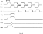
- FIG. 2 illustrating waveforms of signals applied on the scanning driver according to the first embodiment of the present disclosure.
- the scanning driver 10 for driving scan lines row by row includes cascaded scanning circuits.
- Each scanning circuit includes a pull-up holding control module 11, a driving module 12, a pull-down holding module 14, a constant low voltage supply VSS, and a bootstrap capacitor Original Translation Cb.
- the pull-up control module 11 is configured to generate a scan voltage level signal Q(n) in response to a scanning signal from a previous stage scanning circuit.
- the driving module 12 is configured to pull up a scanning signal G(n) outputted to a scan line coupled to a current stage scanning circuit in response to the scan voltage level signal Q(n) and a clock signal CK(n) fed to the current stage scanning circuit.
- the pull-down module 13 is configured to pull down the scan voltage level signal Q(n) in response to a scanning signal from a next stage scanning circuit.
- the pull-down holding module 14 is configured to hold the scan voltage level signal Q(n) at a low voltage level.
- the constant low voltage supply VSS is configured to supply a constant low voltage.
- the bootstrap capacitor Cb is used to generate high voltage of the scanning signal of the current stage scanning circuit G(n).
- the pull-up control module 11 includes a first transistor T1, a second transistor T2, and a third transistor T3.
- the first transistor T1 includes a control terminal coupled to the scanning signal G(n-4) of the previous four stage scanning circuit, an input terminal coupled to the scanning signal G(n-4) of the previous four stage scanning circuit, and an output terminal.
- the second transistor T2 includes a control terminal coupled to the scanning signal G(n-4) of the previous four stage scanning circuit, an input terminal coupled to the output terminal of the first transistor T1, and an output terminal outputting the scan voltage level signal Q(n).
- the third transistor T3 includes a control terminal coupled to the output terminal of the second transistor T2, an input terminal coupled to a constant high voltage level supply VGH, and an output terminal coupled to the input terminal of the second transistor T2.
- the driving module 12 includes a fourth transistor T4 and a fifth transistor T5.
- the fourth transistor T4 includes a control terminal coupled to an output terminal of the pull-up control module 11, an input terminal coupled to the clock signal CK(n), and an output terminal outputting coupled to a start signal ST(n).
- the fifth transistor T5 includes a control terminal coupled to the output terminal of the pull-up control module 11, an input terminal coupled to the clock signal CK(n), and an output terminal outputting coupled to the scanning signal G(n).
- the bootstrap capacitor Cb is connected between the output terminal of the pull-up control module 11 and the output terminal of the fifth transistor T5.
- the pull-down module 13 includes a sixth transistor T6 and a seventh transistor T7.
- the sixth transistor T6 includes a control terminal coupled to scanning signal G(n+5) of the next five stage scanning circuit, an input terminal coupled to the constant low voltage supply VSS, and an output terminal coupled to the output terminal of the second transistor T2.
- the seventh transistor T7 includes a control terminal coupled to the scanning signal G(n+5) of the next five stage scanning circuit, an input terminal coupled to the constant low voltage supply VSS, and an output terminal coupled to the output terminal of the driving module 12.
- the pull-down holding module 14 includes an eighth transistor T8, a ninth transistor T9, a tenth transistor T10, an eleventh transistor T11, a twelfth transistor T12, a thirteenth transistor T13, a fourteenth transistor T14, a fifteenth transistor T15, a sixteenth transistor T16, a seventeenth transistor T17, an eighteenth transistor T18, and a nineteenth transistor T19.
- the eighth transistor T8 includes a control terminal coupled to a first reference node P(n), an input terminal coupled to the constant low voltage supply VSS, and an output terminal coupled to the output terminal of the second transistor T2.
- the ninth transistor T9 includes a control terminal coupled to the first reference node P(n), an input terminal coupled to the constant low voltage supply VSS, and an output terminal coupled to the output terminal of the driving module 12.
- the tenth transistor T10 includes a control terminal coupled to an output terminal of the twelfth transistor T12, an input terminal coupled to a first low frequency voltage level signal LC1, and an output terminal coupled to the first reference node P(n).
- the eleventh transistor T11 includes a control terminal coupled to the output terminal of the second transistor T2, an input terminal coupled to the constant low voltage supply VSS, and an output terminal coupled to the first reference node P(n).
- the twelfth transistor T12 includes a control terminal coupled to the first low frequency voltage level signal LC1, and an input terminal coupled to the first low frequency voltage level signal LC1.
- the thirteenth transistor T13 includes a control terminal coupled to the output terminal of the second transistor T2, an input terminal coupled to the constant low voltage supply VSS, and an output terminal coupled to the control terminal of the tenth transistor T10.
- the fourteenth transistor T14 includes a control terminal coupled to a second reference node K(n), an input terminal coupled to the constant low voltage supply VSS, and an output terminal coupled to the output terminal of the second transistor T2.
- the fifteenth transistor T15 includes a control terminal coupled to the second reference node K(n), an input terminal coupled to the constant low voltage supply VSS, and an output terminal coupled to the output terminal of the driving module 12.
- the sixteenth transistor T16 includes a control terminal coupled to an output terminal of an eighteenth transistor T18, an input terminal coupled to a second low frequency voltage level signal LC2, and an output terminal coupled to the second reference node K(n).
- the seventeenth transistor T17 includes a control terminal coupled to the output terminal of the second transistor T2, an input terminal coupled to the constant low voltage supply VSS, and an output terminal coupled to the second reference node K(n).
- the eighteenth transistor T18 includes a control terminal coupled to the second low frequency voltage level signal LC2, and an input terminal coupled to the second low frequency voltage level signal LC2.
- the nineteenth transistor T19 includes a control terminal coupled to the output terminal of the second transistor T2, an input terminal coupled to the constant low voltage supply VSS, and an output terminal coupled to the control terminal of the sixteenth transistor T16.
- the first low frequency voltage level signal LC1 is inverted to the second low frequency voltage level signal LC2.
- the scanning signal G(n-4) of the previous four stage scanning circuit is at the high voltage level
- the first transistor T1 and the second transistor T2 are conducted.
- the bootstrap capacitor Cb is charged by the scanning signal G(n-4) of the previous four stage scanning circuit through the first transistor T1 and the second transistor T2 to make the scan voltage level signal Q(n) rise to a higher voltage level.
- the scanning signal G(n-4) of the previous four stage scanning circuit is turned into the low voltage level.
- the first transistor T1 and the second transistor T2 are disconnected; the scan voltage level signal Q(n) maintains a higher voltage level through the bootstrap capacitor Cb.
- the third transistor T3 is conducted because of the operation of the scan voltage level signal Q(n) at the high voltage level.
- the constant high voltage level supply VGH is connected to an input terminal of the second transistor T2 though the third transistor T3.
- the voltage difference between the input terminal and the output terminal reduces, and electricity does not leak from the second transistor T2 because of the variation of the voltage imposed on the scanning signal G(n-4) of the previous four stage scanning circuit.
- the reliability of the scanning driver 10 enhances accordingly.
- the following clock signal CK(n) is turned into a high voltage level.
- the clock signal CK(n) continues charging the bootstrap capacitor Cb through the fifth transistor T5 to make the scan voltage level signal Q(n) reach a higher voltage level.
- the current stage scanning signal G(n) is turned into a high voltage level as well.
- a current stage scanning signal G(n) is output through the terminal of the fifth transistor T5.
- a current stage start signal ST(n) is output through the terminal of the fourth transistor T4.
- the eleventh transistor T11, the thirteenth transistor T13, the seventeenth transistor T17, and the nineteenth transistor T19 are conducted because of the operation of the scan voltage level signal Q(n) at the high voltage level. So the first reference node P(n) and the second reference node K(n) keep the high voltage level under the control of the constant low voltage supply VSS. So the eighth transistor T8, the ninth transistor T9, the fourteenth transistor T14, and the fifteenth transistor T15 keep disconnected, which ensures that the scan voltage level signal Q(n) is at the high voltage level.
- a scanning signal G(n+5) of the next five stage scanning circuit is turned into a high voltage level, a sixth transistor T6 and a seventh transistor T7 are conducted, and the scan voltage level signal Q(n) is pulled to a low voltage level by the constant low voltage supply VSS. Meanwhile, the eleventh transistor T11, the thirteenth transistor T13, the seventeenth transistor T17, and the nineteenth transistor T19 are disconnected.
- the pull-down holding module 14 holds the low voltage level of the scan voltage level signal Q(n) because of the operation of a first low frequency voltage level signal LC1 and a second low frequency voltage level signal LC2.
- the twelfth transistor T12 and the tenth transistor T10 are conducted.
- the first reference node P(n) is pulled to the high voltage level through the tenth transistor T10.
- the eighth transistor T8 and the ninth transistor T9 are conducted.
- the scan voltage level signal Q(n) is connected to the constant low voltage supply VSS through the eighth transistor T8, which keeps the scan voltage level signal Q(n) at the low voltage level.
- the current stage scanning signal G(n) is connected to the constant low voltage supply VSS through the ninth transistor T9, which keeps the current stage scanning signal G(n) at the low voltage level.
- the sixteenth transistor T16 and the eighteenth transistor T18 are conducted.
- the second reference node K(n) is pulled to the high voltage level through the sixteenth transistor T16.
- the fourteenth transistor T14 and the fifteenth transistor T15 are conducted.
- the scan voltage level signal Q(n) is connected to the constant low voltage supply VSS through the fifteenth transistor T15, which keeps the scan voltage level signal Q(n) at the low voltage level.
- the current stage scanning signal G(n) is connected to the constant low voltage supply VSS through the fourteenth transistor T14, which keeps the current stage scanning signal G(n) at the low voltage level.
- the scanning signal G(n-4) of the previous four stage scanning circuit is turned into the low voltage level.
- the scan voltage level signal Q(n) keeps at the high voltage level better, which prevents current from being leaked.
- the current stage scanning signal G(n) and the scan voltage level signal Q(n) are the scanning signal and the scan voltage level signal in the scanning driver 10 proposed by embodiment of the present disclosure.
- the current stage scanning signal G(n)' and the scan voltage level signal Q(n)' are the scanning signal and the scan voltage level signal in the conventional scanning driver.
- FIG. 2 shows, the waveform of the current stage scanning signal G(n) and the waveform of the scan voltage level signal Q(n) are improved more obviously under the operation of the pull-up holding control module 11.
- the pull-up control module including the plurality of transistors is arranged on the scanning driver 10 proposed by embodiment of the present disclosure. Such a design is beneficial to prevent electricity from leaking and enhance the stability of the scanning driver 10.
- FIG. 3 illustrating a circuit diagram of a scanning driver according to a second embodiment of the present disclosure.
- an input terminal of a third transistor T3' of a pull-up control module of the scanning driver is connected to an output terminal of a driving module; that is, a current stage scanning signal G(n) is input to the third transistor T3'.
- the arrangement also makes the scan voltage level signal Q(n) keep the high voltage level. Further, it is unnecessary to use an additional constant high voltage level supply VGH.
- the specific operating principle of the scanning driver proposed by the second embodiment is the same as or similar to the scanning driver proposed by the first embodiment so the details of the scanning driver can refer to the first embodiment.
- the present disclosure also proposes a display device including a scanning driver for driving scan lines row by row.
- the scanning driver includes cascaded scanning circuits.
- Each scanning circuit includes a pull-up holding control module 11, a driving module 12, a pull-down holding module 14, a constant low voltage supply VSS, and a bootstrap capacitor Cb as illustrated in FIG. 1 .
- the pull-up control module 11 is configured to generate a scan voltage level signal Q(n) in response to a scanning signal from a previous stage scanning circuit.
- the driving module 12 is configured to pull up a scanning signal G(n) outputted to a scan line coupled to a current stage scanning circuit in response to the scan voltage level signal Q(n) and a clock signal CK(n) fed to the current stage scanning circuit.
- the pull-down module 13 is configured to pull down the scan voltage level signal Q(n) in response to a scanning signal from a next stage scanning circuit.
- the pull-down holding module 14 is configured to hold the scan voltage level signal Q(n) at a low voltage level.
- the constant low voltage supply VSS is configured to supply a constant low voltage.
- the bootstrap capacitor Cb is used to generate high voltage of the scanning signal of the current stage scanning circuit G(n).
- the pull-up control module 11 includes a first transistor T1, a second transistor T2, and a third transistor T3.
- the first transistor T1 includes a control terminal coupled to the scanning signal G(n-4) of the previous four stage scanning circuit, an input terminal coupled to the scanning signal G(n-4) of the previous four stage scanning circuit, and an output terminal.
- the second transistor T2 includes a control terminal coupled to the scanning signal G(n-4) of the previous four stage scanning circuit, an input terminal coupled to the output terminal of the first transistor T1, and an output terminal outputting the scan voltage level signal Q(n).
- the third transistor T3 includes a control terminal coupled to the output terminal of the second transistor T2, an input terminal coupled to a constant high voltage level supply VGH, and an output terminal coupled to the input terminal of the second transistor T2.
- the scanning signal G(n-4) of the previous four stage scanning circuit and scanning signal G(n+5) of the next five stage scanning circuit are used in the present disclosure.
- the driving module 12 includes a fourth transistor T4 and a fifth transistor T5.
- the fourth transistor T4 includes a control terminal coupled to an output terminal of the pull-up control module 11, an input terminal coupled to the clock signal CK(n), and an output terminal outputting coupled to a start signal ST(n).
- the fifth transistor T5 includes a control terminal coupled to the output terminal of the pull-up control module 11, an input terminal coupled to the clock signal CK(n), and an output terminal outputting coupled to the scanning signal G(n).
- the bootstrap capacitor Cb is connected between the output terminal of the pull-up control module 11 and the output terminal of the fifth transistor T5.
- the pull-down module 13 includes a sixth transistor T6 and a seventh transistor T7.
- the sixth transistor T6 includes a control terminal coupled to scanning signal G(n+5) of the next five stage scanning circuit, an input terminal coupled to the constant low voltage supply VSS, and an output terminal coupled to the output terminal of the second transistor T2.
- the seventh transistor T7 includes a control terminal coupled to the scanning signal G(n+5) of the next five stage scanning circuit, an input terminal coupled to the constant low voltage supply VSS, and an output terminal coupled to the output terminal of the driving module 12.
- the pull-down holding module 14 includes an eighth transistor T8, a ninth transistor T9, a tenth transistor T10, an eleventh transistor T11, a twelfth transistor T12, a thirteenth transistor T13, a fourteenth transistor T14, a fifteenth transistor T15, a sixteenth transistor T16, a seventeenth transistor T17, an eighteenth transistor T18, and a nineteenth transistor T19.
- the eighth transistor T8 includes a control terminal coupled to a first reference node P(n), an input terminal coupled to the constant low voltage supply VSS, and an output terminal coupled to the output terminal of the second transistor T2.
- the ninth transistor T9 includes a control terminal coupled to the first reference node P(n), an input terminal coupled to the constant low voltage supply VSS, and an output terminal coupled to the output terminal of the driving module 12.
- the tenth transistor T10 includes a control terminal coupled to an output terminal of the twelfth transistor T12, an input terminal coupled to a first low frequency voltage level signal LC1, and an output terminal coupled to the first reference node P(n).
- the eleventh transistor T11 includes a control terminal coupled to the output terminal of the second transistor T2, an input terminal coupled to the constant low voltage supply VSS, and an output terminal coupled to the first reference node P(n).
- the twelfth transistor T12 includes a control terminal coupled to the first low frequency voltage level signal LC1, and an input terminal coupled to the first low frequency voltage level signal LC1.
- the thirteenth transistor T13 includes a control terminal coupled to the output terminal of the second transistor T2, an input terminal coupled to the constant low voltage supply VSS, and an output terminal coupled to the control terminal of the tenth transistor T10.
- the fourteenth transistor T14 includes a control terminal coupled to a second reference node K(n), an input terminal coupled to the constant low voltage supply VSS, and an output terminal coupled to the output terminal of the second transistor T2.
- the fifteenth transistor T15 includes a control terminal coupled to the second reference node K(n), an input terminal coupled to the constant low voltage supply VSS, and an output terminal coupled to the output terminal of the driving module 12.
- the sixteenth transistor T16 includes a control terminal coupled to an output terminal of an eighteenth transistor T18, an input terminal coupled to a second low frequency voltage level signal LC2, and an output terminal coupled to the second reference node K(n).
- the seventeenth transistor T17 includes a control terminal coupled to the output terminal of the second transistor T2, an input terminal coupled to the constant low voltage supply VSS, and an output terminal coupled to the second reference node K(n).
- the eighteenth transistor T18 includes a control terminal coupled to the second low frequency voltage level signal LC2, and an input terminal coupled to the second low frequency voltage level signal LC2.
- the nineteenth transistor T19 includes a control terminal coupled to the output terminal of the second transistor T2, an input terminal coupled to the constant low voltage supply VSS, and an output terminal coupled to the control terminal of the sixteenth transistor T16.
- the first low frequency voltage level signal LC1 is inverted to the second low frequency voltage level signal LC2.
- the specific operating principle of the scanning driver of the display device is the same as or similar to the scanning driver proposed by the first embodiment so the details of the scanning driver can refer to the first embodiment.
- the present disclosure proposes a scanning driver and a display device.
- the scanning driver arranged on the display device utilizes the pull-up control module including a plurality of transistors.
- the merits of the present disclosure are to prevent from leaking current and to enhance the reliability of the scanning driver.
- the present disclosure can solve the technical problem that the conventional scanning driver and the conventional display device are inclined to leak electricity, thereby enhancing the reliability of the scanning driver.
Landscapes
- Engineering & Computer Science (AREA)
- Theoretical Computer Science (AREA)
- Physics & Mathematics (AREA)
- Crystallography & Structural Chemistry (AREA)
- Computer Hardware Design (AREA)
- General Physics & Mathematics (AREA)
- Chemical & Material Sciences (AREA)
- Power Engineering (AREA)
- Control Of Indicators Other Than Cathode Ray Tubes (AREA)
- Electronic Switches (AREA)
- Liquid Crystal (AREA)
- Shift Register Type Memory (AREA)
- Liquid Crystal Display Device Control (AREA)
Abstract
Description
- The present disclosure relates to the field of liquid crystal displays (LCDs), and more particularly to a gate driver on array (GOA) driving circuit and an LCD device.
- A gate driver on array circuit (abbreviated as GOA circuit) uses a scan driving circuit that is formed on an array substrate by processing of an array substrate of a traditional thin film transistor-liquid crystal display (TFT-LCD), thus, a driving method for scanning a pixel structure row by row is achieved.
- A conventional scan driving circuit includes a plurality of GOA unit. Each GOA unit for driving a scan line includes a pull-up control module, a driving module, a pull-down module, and a pull-down holding module.
- The conventional pull-up control module is usually formed by one single transistor. The threshold of a voltage imposed on the transistor tends to become a negative value when the scan driving circuit works in the high temperature condition. Accordingly, the transistor in the pull-up control module is inclined to leak electricity. Further, the variation of an input signal in the pull-up control module may have a big influence on an output signal in the driving module, which affects the reliability of the scanning driver.
- Therefore, the prior art is defective and needs to be improved and developed.
- It is therefore an objective of the present disclosure to provide a gate driver on array (GOA) circuit and a liquid crystal display (LCD) device with low current leakage and high reliability to solve the technical issue of conventional scan driving circuit.
- According to the present disclosure, a scanning driver for driving scan lines row by row is provided. The scanning driver comprises cascaded scanning circuits. Each scanning circuit comprises:
- a pull-up control module, configured to generate a scan voltage level signal in response to a scanning signal from a previous stage scanning circuit;
- a driving module, configured to pull up a scanning signal outputted to a scan line coupled to a current stage scanning circuit in response to the scan voltage level signal and a clock signal fed to the current stage scanning circuit;
- a pull-down module, configured to pull down the scan voltage level signal in response to a scanning signal from a next stage scanning circuit;
- a pull-down holding module, configured to hold the scan voltage level signal at a low voltage level; and
- a constant low voltage supply, configured to supply a constant low voltage,
- wherein the pull-up control module comprises: a first transistor comprising a control terminal coupled to the scanning signal of the previous stage scanning circuit, an input terminal coupled to the scanning signal of the previous stage scanning circuit, and an output terminal; a second transistor, comprising a control terminal coupled to the scanning signal of the previous stage scanning circuit, an input terminal coupled to the output terminal of the first transistor, and an output terminal outputting the scan voltage level signal; a third transistor, comprising a control terminal coupled to the output terminal of the second transistor, an input terminal coupled to a constant high voltage level supply, and an output terminal coupled to the input terminal of the second transistor .
- Optionally, the scanning signal from the previous stage scanning circuit is the scanning signal from a previous four stage scanning circuit, and the scanning signal from the next stage scanning circuit is the scanning signal from a next five stage scanning circuit.
- Optionally, the driving module comprises:
- a fourth transistor, comprising a control terminal coupled to an output terminal of the pull-up control module, an input terminal coupled to the clock signal, and an output terminal outputting coupled to a start signal;
- a fifth transistor, comprising a control terminal coupled to the output terminal of the pull-up control module, an input terminal coupled to the clock signal, and an output terminal outputting coupled to the scanning signal.
- Optionally, the scanning driver further comprises a bootstrap capacitor, connected between the output terminal of the pull-up control module and the output terminal of the fifth transistor, for generating high voltage of the scanning signal of the current stage scanning circuit.
- Optionally, the pull-down module comprises:
- a sixth transistor comprising a control terminal coupled to scanning signal of the next stage scanning circuit, an input terminal coupled to the constant low voltage supply, and an output terminal coupled to the output terminal of the second transistor;
- a seventh transistor comprising a control terminal coupled to the scanning signal of the next stage scanning circuit, an input terminal coupled to the constant low voltage supply, and an output terminal coupled to the output terminal of the driving module.
- Optionally, the pull-down holding module comprises:
- an eighth transistor comprising a control terminal coupled to a first reference node, an input terminal coupled to the constant low voltage supply, and an output terminal coupled to the output terminal of the second transistor;
- a ninth transistor comprising a control terminal coupled to the first reference node, an input terminal coupled to the constant low voltage supply, and an output terminal coupled to the output terminal of the driving module;
- a tenth transistor comprising a control terminal coupled to an output terminal of a twelfth transistor, an input terminal coupled to a first low frequency voltage level signal, and an output terminal coupled to the first reference node;
- an eleventh transistor comprising a control terminal coupled to the output terminal of the second transistor, an input terminal coupled to the constant low voltage supply, and an output terminal coupled to the first reference node;
- the twelfth transistor comprising a control terminal coupled to the first low frequency voltage level signal, and an input terminal coupled to the first low frequency voltage level signal;
- a thirteenth transistor comprising a control terminal coupled to the output terminal of the second transistor, an input terminal coupled to the constant low voltage supply, and an output terminal coupled to the control terminal of the tenth transistor;
- a fourteenth transistor comprising a control terminal coupled to a second reference node, an input terminal coupled to the constant low voltage supply, and an output terminal coupled to the output terminal of the second transistor;
- a fifteenth transistor comprising a control terminal coupled to the second reference node, an input terminal coupled to the constant low voltage supply, and an output terminal coupled to the output terminal of the driving module;
- a sixteenth transistor comprising a control terminal coupled to an output terminal of an eighteenth transistor, an input terminal coupled to a second low frequency voltage level signal, and an output terminal coupled to the second reference node;
- a seventeenth transistor comprising a control terminal coupled to the output terminal of the second transistor, an input terminal coupled to the constant low voltage supply, and an output terminal coupled to the second reference node;
- the eighteenth transistor comprising a control terminal coupled to the second low frequency voltage level signal, and an input terminal coupled to the second low frequency voltage level signal; and
- a nineteenth transistor comprising a control terminal coupled to the output terminal of the second transistor, an input terminal coupled to the constant low voltage supply, and an output terminal coupled to the control terminal of the sixteenth transistor.
- Optionally, the first low frequency voltage level signal are inverted to the second low frequency voltage level signal.
- According to the present disclosure, a scanning driver for driving scan lines row by row is provided. The scanning driver comprises cascaded scanning circuits. Each scanning circuit comprises:
- a pull-up control module, configured to generate a scan voltage level signal in response to a scanning signal from a previous stage scanning circuit;
- a driving module, configured to pull up a scanning signal outputted to a scan line coupled to a current stage scanning circuit in response to the scan voltage level signal and a clock signal fed to the current stage scanning circuit;
- a pull-down module, configured to pull down the scan voltage level signal in response to a scanning signal from a next stage scanning circuit;
- a pull-down holding module, configured to hold the scan voltage level signal at a low voltage level; and
- a constant low voltage supply, configured to supply a constant low voltage,
- wherein the pull-up control module comprises: a first transistor comprising a control terminal coupled to the scanning signal of the previous stage scanning circuit, an input terminal coupled to the scanning signal of the previous stage scanning circuit, and an output terminal; a second transistor, comprising a control terminal coupled to the scanning signal of the previous stage scanning circuit, an input terminal coupled to the output terminal of the first transistor, and an output terminal outputting the scan voltage level signal; a third transistor, comprising a control terminal coupled to the output terminal of the second transistor, an input terminal coupled to an output terminal of the driving module, and an output terminal coupled to the input terminal of the second transistor .
- Optionally, the scanning signal from the previous stage scanning circuit is the scanning signal from a previous four stage scanning circuit, and the scanning signal from the next stage scanning circuit is the scanning signal from a next five stage scanning circuit.
- Optionally, the driving module comprises:
- a fourth transistor, comprising a control terminal coupled to an output terminal of the pull-up control module, an input terminal coupled to the clock signal, and an output terminal outputting coupled to a start signal;
- a fifth transistor, comprising a control terminal coupled to the output terminal of the pull-up control module, an input terminal coupled to the clock signal, and an output terminal outputting coupled to the scanning signal.
- Optionally, the scanning driver further comprises a bootstrap capacitor, connected between the output terminal of the pull-up control module and the output terminal of the fifth transistor, for generating high voltage of the scanning signal of the current stage scanning circuit.
- Optionally, the pull-down module comprises:
- a sixth transistor comprising a control terminal coupled to scanning signal of the next stage scanning circuit, an input terminal coupled to the constant low voltage supply, and an output terminal coupled to the output terminal of the second transistor;
- a seventh transistor comprising a control terminal coupled to the scanning signal of the next stage scanning circuit, an input terminal coupled to the constant low voltage supply, and an output terminal coupled to the output terminal of the driving module.
- Optionally, the pull-down holding module comprises:
- an eighth transistor comprising a control terminal coupled to a first reference node, an input terminal coupled to the constant low voltage supply, and an output terminal coupled to the output terminal of the second transistor;
- a ninth transistor comprising a control terminal coupled to the first reference node, an input terminal coupled to the constant low voltage supply, and an output terminal coupled to the output terminal of the driving module;
- a tenth transistor comprising a control terminal coupled to an output terminal of a twelfth transistor, an input terminal coupled to a first low frequency voltage level signal, and an output terminal coupled to the first reference node;
- an eleventh transistor comprising a control terminal coupled to the output terminal of the second transistor, an input terminal coupled to the constant low voltage supply, and an output terminal coupled to the first reference node;
- the twelfth transistor comprising a control terminal coupled to the first low frequency voltage level signal, and an input terminal coupled to the first low frequency voltage level signal;
- a thirteenth transistor comprising a control terminal coupled to the output terminal of the second transistor, an input terminal coupled to the constant low voltage supply, and an output terminal coupled to the control terminal of the tenth transistor;
- a fourteenth transistor comprising a control terminal coupled to a second reference node, an input terminal coupled to the constant low voltage supply, and an output terminal coupled to the output terminal of the second transistor;
- a fifteenth transistor comprising a control terminal coupled to the second reference node, an input terminal coupled to the constant low voltage supply, and an output terminal coupled to the output terminal of the driving module;
- a sixteenth transistor comprising a control terminal coupled to an output terminal of an eighteenth transistor, an input terminal coupled to a second low frequency voltage level signal, and an output terminal coupled to the second reference node;
- a seventeenth transistor comprising a control terminal coupled to the output terminal of the second transistor, an input terminal coupled to the constant low voltage supply, and an output terminal coupled to the second reference node;
- the eighteenth transistor comprising a control terminal coupled to the second low frequency voltage level signal, and an input terminal coupled to the second low frequency voltage level signal; and
- a nineteenth transistor comprising a control terminal coupled to the output terminal of the second transistor, an input terminal coupled to the constant low voltage supply, and an output terminal coupled to the control terminal of the sixteenth transistor.
- Optionally, the first low frequency voltage level signal are inverted to the second low frequency voltage level signal.
- According to the present disclosure, a display device having a scanning driver for driving scan lines row by row is provided. The scanning driver comprises cascaded scanning circuits. Each scanning circuit comprises:
- a pull-up control module, configured to generate a scan voltage level signal in response to a scanning signal from a previous stage scanning circuit;
- a driving module, configured to pull up a scanning signal outputted to a scan line coupled to a current stage scanning circuit in response to the scan voltage level signal and a clock signal fed to the current stage scanning circuit;
- a pull-down module, configured to pull down the scan voltage level signal in response to a scanning signal from a next stage scanning circuit;
- a pull-down holding module, configured to hold the scan voltage level signal at a low voltage level; and
- a constant low voltage supply, configured to supply a constant low voltage,
- wherein the pull-up control module comprises: a first transistor comprising a control terminal coupled to the scanning signal of the previous stage scanning circuit, an input terminal coupled to the scanning signal of the previous stage scanning circuit, and an output terminal; a second transistor, comprising a control terminal coupled to the scanning signal of the previous stage scanning circuit, an input terminal coupled to the output terminal of the first transistor, and an output terminal outputting the scan voltage level signal; a third transistor, comprising a control terminal coupled to the output terminal of the second transistor, an input terminal coupled to a constant high voltage level supply, and an output terminal coupled to the input terminal of the second transistor .
- Optionally, the scanning signal from the previous stage scanning circuit is the scanning signal from a previous four stage scanning circuit, and the scanning signal from the next stage scanning circuit is the scanning signal from a next five stage scanning circuit.
- Optionally, the driving module comprises:
- a fourth transistor, comprising a control terminal coupled to an output terminal of the pull-up control module, an input terminal coupled to the clock signal, and an output terminal outputting coupled to a start signal;
- a fifth transistor, comprising a control terminal coupled to the output terminal of the pull-up control module, an input terminal coupled to the clock signal, and an output terminal outputting coupled to the scanning signal.
- Optionally, the scanning driver further comprises a bootstrap capacitor, connected between the output terminal of the pull-up control module and the output terminal of the fifth transistor, for generating high voltage of the scanning signal of the current stage scanning circuit.
- Optionally, the pull-down module comprises:
- a sixth transistor comprising a control terminal coupled to scanning signal of the next stage scanning circuit, an input terminal coupled to the constant low voltage supply, and an output terminal coupled to the output terminal of the second transistor;
- a seventh transistor comprising a control terminal coupled to the scanning signal of the next stage scanning circuit, an input terminal coupled to the constant low voltage supply, and an output terminal coupled to the output terminal of the driving module.
- Optionally, the pull-down holding module comprises:
- an eighth transistor comprising a control terminal coupled to a first reference node, an input terminal coupled to the constant low voltage supply, and an output terminal coupled to the output terminal of the second transistor;
- a ninth transistor comprising a control terminal coupled to the first reference node, an input terminal coupled to the constant low voltage supply, and an output terminal coupled to the output terminal of the driving module;
- a tenth transistor comprising a control terminal coupled to an output terminal of a twelfth transistor, an input terminal coupled to a first low frequency voltage level signal, and an output terminal coupled to the first reference node;
- an eleventh transistor comprising a control terminal coupled to the output terminal of the second transistor, an input terminal coupled to the constant low voltage supply, and an output terminal coupled to the first reference node;
- the twelfth transistor comprising a control terminal coupled to the first low frequency voltage level signal, and an input terminal coupled to the first low frequency voltage level signal;
- a thirteenth transistor comprising a control terminal coupled to the output terminal of the second transistor, an input terminal coupled to the constant low voltage supply, and an output terminal coupled to the control terminal of the tenth transistor;
- a fourteenth transistor comprising a control terminal coupled to a second reference node, an input terminal coupled to the constant low voltage supply, and an output terminal coupled to the output terminal of the second transistor;
- a fifteenth transistor comprising a control terminal coupled to the second reference node, an input terminal coupled to the constant low voltage supply, and an output terminal coupled to the output terminal of the driving module;
- a sixteenth transistor comprising a control terminal coupled to an output terminal of an eighteenth transistor, an input terminal coupled to a second low frequency voltage level signal, and an output terminal coupled to the second reference node;
- a seventeenth transistor comprising a control terminal coupled to the output terminal of the second transistor, an input terminal coupled to the constant low voltage supply, and an output terminal coupled to the second reference node;
- the eighteenth transistor comprising a control terminal coupled to the second low frequency voltage level signal, and an input terminal coupled to the second low frequency voltage level signal; and
- a nineteenth transistor comprising a control terminal coupled to the output terminal of the second transistor, an input terminal coupled to the constant low voltage supply, and an output terminal coupled to the control terminal of the sixteenth transistor.
- The present disclosure proposes a scanning driver and a display device. The scanning driver arranged on the display device utilizes the pull-up control module including a plurality of transistors. Compared with the conventional scanning driver and the conventional display device, the merits of the present disclosure are to prevent from leaking current and to enhance the reliability of the scanning driver. The present disclosure can solve the technical problem that the conventional scanning driver and the conventional display device are inclined to leak electricity, thereby enhancing the reliability of the scanning driver.
- These and other features, aspects and advantages of the present disclosure will become understood with reference to the following description, appended claims and accompanying figures.
-
-
FIG. 1 illustrates a circuit diagram of a scanning driver according to a first embodiment of the present disclosure. -
FIG. 2 illustrates waveforms of signals applied on the scanning driver according to the first embodiment of the present disclosure. -
FIG. 3 illustrates a circuit diagram of a scanning driver according to a second embodiment of the present disclosure. - The following description of every embodiment with reference to the accompanying drawings is used to exemplify a specific embodiment, which may be carried out in the present invention. Directional terms mentioned in the present invention, such as "top", "bottom", "front", "back", "left", "right", "inside", "outside", "side" etc., are only used with reference to the orientation of the accompanying drawings. Therefore, the used directional terms are intended to illustrate, but not to limit, the present invention.
- In the drawings, the components having similar structures are denoted by the same numerals.
- Please refer to
FIG. 1 illustrating a circuit diagram of a scanning driver according to a first embodiment of the present disclosure, andFIG. 2 illustrating waveforms of signals applied on the scanning driver according to the first embodiment of the present disclosure. Thescanning driver 10 for driving scan lines row by row, includes cascaded scanning circuits. Each scanning circuit includes a pull-up holdingcontrol module 11, a drivingmodule 12, a pull-downholding module 14, a constant low voltage supply VSS, and a bootstrap capacitor Original Translation Cb. - The pull-up
control module 11 is configured to generate a scan voltage level signal Q(n) in response to a scanning signal from a previous stage scanning circuit. The drivingmodule 12 is configured to pull up a scanning signal G(n) outputted to a scan line coupled to a current stage scanning circuit in response to the scan voltage level signal Q(n) and a clock signal CK(n) fed to the current stage scanning circuit. The pull-down module 13 is configured to pull down the scan voltage level signal Q(n) in response to a scanning signal from a next stage scanning circuit. The pull-downholding module 14 is configured to hold the scan voltage level signal Q(n) at a low voltage level. The constant low voltage supply VSS is configured to supply a constant low voltage. The bootstrap capacitor Cb, is used to generate high voltage of the scanning signal of the current stage scanning circuit G(n). - The pull-up
control module 11 includes a first transistor T1, a second transistor T2, and a third transistor T3. The first transistor T1 includes a control terminal coupled to the scanning signal G(n-4) of the previous four stage scanning circuit, an input terminal coupled to the scanning signal G(n-4) of the previous four stage scanning circuit, and an output terminal. The second transistor T2 includes a control terminal coupled to the scanning signal G(n-4) of the previous four stage scanning circuit, an input terminal coupled to the output terminal of the first transistor T1, and an output terminal outputting the scan voltage level signal Q(n). The third transistor T3 includes a control terminal coupled to the output terminal of the second transistor T2, an input terminal coupled to a constant high voltage level supply VGH, and an output terminal coupled to the input terminal of the second transistor T2. - The driving
module 12 includes a fourth transistor T4 and a fifth transistor T5. The fourth transistor T4 includes a control terminal coupled to an output terminal of the pull-upcontrol module 11, an input terminal coupled to the clock signal CK(n), and an output terminal outputting coupled to a start signal ST(n). The fifth transistor T5 includes a control terminal coupled to the output terminal of the pull-upcontrol module 11, an input terminal coupled to the clock signal CK(n), and an output terminal outputting coupled to the scanning signal G(n). - The bootstrap capacitor Cb is connected between the output terminal of the pull-up
control module 11 and the output terminal of the fifth transistor T5. - The pull-
down module 13 includes a sixth transistor T6 and a seventh transistor T7. The sixth transistor T6 includes a control terminal coupled to scanning signal G(n+5) of the next five stage scanning circuit, an input terminal coupled to the constant low voltage supply VSS, and an output terminal coupled to the output terminal of the second transistor T2. The seventh transistor T7 includes a control terminal coupled to the scanning signal G(n+5) of the next five stage scanning circuit, an input terminal coupled to the constant low voltage supply VSS, and an output terminal coupled to the output terminal of the drivingmodule 12. - The pull-down
holding module 14 includes an eighth transistor T8, a ninth transistor T9, a tenth transistor T10, an eleventh transistor T11, a twelfth transistor T12, a thirteenth transistor T13, a fourteenth transistor T14, a fifteenth transistor T15, a sixteenth transistor T16, a seventeenth transistor T17, an eighteenth transistor T18, and a nineteenth transistor T19. - The eighth transistor T8 includes a control terminal coupled to a first reference node P(n), an input terminal coupled to the constant low voltage supply VSS, and an output terminal coupled to the output terminal of the second transistor T2.
- The ninth transistor T9 includes a control terminal coupled to the first reference node P(n), an input terminal coupled to the constant low voltage supply VSS, and an output terminal coupled to the output terminal of the driving
module 12. - The tenth transistor T10 includes a control terminal coupled to an output terminal of the twelfth transistor T12, an input terminal coupled to a first low frequency voltage level signal LC1, and an output terminal coupled to the first reference node P(n).
- The eleventh transistor T11 includes a control terminal coupled to the output terminal of the second transistor T2, an input terminal coupled to the constant low voltage supply VSS, and an output terminal coupled to the first reference node P(n).
- The twelfth transistor T12 includes a control terminal coupled to the first low frequency voltage level signal LC1, and an input terminal coupled to the first low frequency voltage level signal LC1.
- The thirteenth transistor T13 includes a control terminal coupled to the output terminal of the second transistor T2, an input terminal coupled to the constant low voltage supply VSS, and an output terminal coupled to the control terminal of the tenth transistor T10.
- The fourteenth transistor T14 includes a control terminal coupled to a second reference node K(n), an input terminal coupled to the constant low voltage supply VSS, and an output terminal coupled to the output terminal of the second transistor T2.
- The fifteenth transistor T15 includes a control terminal coupled to the second reference node K(n), an input terminal coupled to the constant low voltage supply VSS, and an output terminal coupled to the output terminal of the driving
module 12. - The sixteenth transistor T16 includes a control terminal coupled to an output terminal of an eighteenth transistor T18, an input terminal coupled to a second low frequency voltage level signal LC2, and an output terminal coupled to the second reference node K(n).
- The seventeenth transistor T17 includes a control terminal coupled to the output terminal of the second transistor T2, an input terminal coupled to the constant low voltage supply VSS, and an output terminal coupled to the second reference node K(n).
- The eighteenth transistor T18 includes a control terminal coupled to the second low frequency voltage level signal LC2, and an input terminal coupled to the second low frequency voltage level signal LC2.
- The nineteenth transistor T19 includes a control terminal coupled to the output terminal of the second transistor T2, an input terminal coupled to the constant low voltage supply VSS, and an output terminal coupled to the control terminal of the sixteenth transistor T16.
- The first low frequency voltage level signal LC1 is inverted to the second low frequency voltage level signal LC2.
- Please refer to
FIG. 1 andFig. 2 . When the scanning signal G(n-4) of the previous four stage scanning circuit is at the high voltage level, the first transistor T1 and the second transistor T2 are conducted. The bootstrap capacitor Cb is charged by the scanning signal G(n-4) of the previous four stage scanning circuit through the first transistor T1 and the second transistor T2 to make the scan voltage level signal Q(n) rise to a higher voltage level. Afterwards, the scanning signal G(n-4) of the previous four stage scanning circuit is turned into the low voltage level. The first transistor T1 and the second transistor T2 are disconnected; the scan voltage level signal Q(n) maintains a higher voltage level through the bootstrap capacitor Cb. Meanwhile, the third transistor T3 is conducted because of the operation of the scan voltage level signal Q(n) at the high voltage level. The constant high voltage level supply VGH is connected to an input terminal of the second transistor T2 though the third transistor T3. As a result, the voltage difference between the input terminal and the output terminal reduces, and electricity does not leak from the second transistor T2 because of the variation of the voltage imposed on the scanning signal G(n-4) of the previous four stage scanning circuit. The reliability of thescanning driver 10 enhances accordingly. - The following clock signal CK(n) is turned into a high voltage level. The clock signal CK(n) continues charging the bootstrap capacitor Cb through the fifth transistor T5 to make the scan voltage level signal Q(n) reach a higher voltage level. The current stage scanning signal G(n) is turned into a high voltage level as well.
- At this time, the fourth transistor T4 and the fifth transistor T5 are conducted. A current stage scanning signal G(n) is output through the terminal of the fifth transistor T5. A current stage start signal ST(n) is output through the terminal of the fourth transistor T4.
- The eleventh transistor T11, the thirteenth transistor T13, the seventeenth transistor T17, and the nineteenth transistor T19 are conducted because of the operation of the scan voltage level signal Q(n) at the high voltage level. So the first reference node P(n) and the second reference node K(n) keep the high voltage level under the control of the constant low voltage supply VSS. So the eighth transistor T8, the ninth transistor T9, the fourteenth transistor T14, and the fifteenth transistor T15 keep disconnected, which ensures that the scan voltage level signal Q(n) is at the high voltage level.
- When a scanning signal G(n+5) of the next five stage scanning circuit is turned into a high voltage level, a sixth transistor T6 and a seventh transistor T7 are conducted, and the scan voltage level signal Q(n) is pulled to a low voltage level by the constant low voltage supply VSS. Meanwhile, the eleventh transistor T11, the thirteenth transistor T13, the seventeenth transistor T17, and the nineteenth transistor T19 are disconnected. The pull-down
holding module 14 holds the low voltage level of the scan voltage level signal Q(n) because of the operation of a first low frequency voltage level signal LC1 and a second low frequency voltage level signal LC2. - When the first low frequency voltage level signal LC1 is at the high voltage level and the second low frequency voltage level signal LC2 is at the low voltage level, the twelfth transistor T12 and the tenth transistor T10 are conducted. The first reference node P(n) is pulled to the high voltage level through the tenth transistor T10. The eighth transistor T8 and the ninth transistor T9 are conducted. The scan voltage level signal Q(n) is connected to the constant low voltage supply VSS through the eighth transistor T8, which keeps the scan voltage level signal Q(n) at the low voltage level. The current stage scanning signal G(n) is connected to the constant low voltage supply VSS through the ninth transistor T9, which keeps the current stage scanning signal G(n) at the low voltage level.
- When the first low frequency voltage level signal LC1 is at the low voltage level and the second low frequency voltage level signal LC2 is at the high voltage level, the sixteenth transistor T16 and the eighteenth transistor T18 are conducted. The second reference node K(n) is pulled to the high voltage level through the sixteenth transistor T16. The fourteenth transistor T14 and the fifteenth transistor T15 are conducted. The scan voltage level signal Q(n) is connected to the constant low voltage supply VSS through the fifteenth transistor T15, which keeps the scan voltage level signal Q(n) at the low voltage level. The current stage scanning signal G(n) is connected to the constant low voltage supply VSS through the fourteenth transistor T14, which keeps the current stage scanning signal G(n) at the low voltage level.
- To sum up, because the first transistor T1, the second transistor T2, and the third transistor T3 are arranged on the pull-up holding
control module 11 of thescanning driver 10, the scanning signal G(n-4) of the previous four stage scanning circuit is turned into the low voltage level. The scan voltage level signal Q(n) keeps at the high voltage level better, which prevents current from being leaked. - Please refer to
FIG. 2 carefully. The current stage scanning signal G(n) and the scan voltage level signal Q(n) are the scanning signal and the scan voltage level signal in thescanning driver 10 proposed by embodiment of the present disclosure. The current stage scanning signal G(n)' and the scan voltage level signal Q(n)' are the scanning signal and the scan voltage level signal in the conventional scanning driver. AsFIG. 2 shows, the waveform of the current stage scanning signal G(n) and the waveform of the scan voltage level signal Q(n) are improved more obviously under the operation of the pull-up holdingcontrol module 11. - The pull-up control module including the plurality of transistors is arranged on the
scanning driver 10 proposed by embodiment of the present disclosure. Such a design is beneficial to prevent electricity from leaking and enhance the stability of thescanning driver 10. - Please refer to
FIG. 3 illustrating a circuit diagram of a scanning driver according to a second embodiment of the present disclosure. Based on the first embodiment, an input terminal of a third transistor T3' of a pull-up control module of the scanning driver is connected to an output terminal of a driving module; that is, a current stage scanning signal G(n) is input to the third transistor T3'. The arrangement also makes the scan voltage level signal Q(n) keep the high voltage level. Further, it is unnecessary to use an additional constant high voltage level supply VGH. - The specific operating principle of the scanning driver proposed by the second embodiment is the same as or similar to the scanning driver proposed by the first embodiment so the details of the scanning driver can refer to the first embodiment.
- The present disclosure also proposes a display device including a scanning driver for driving scan lines row by row. The scanning driver includes cascaded scanning circuits. Each scanning circuit includes a pull-up holding
control module 11, a drivingmodule 12, a pull-downholding module 14, a constant low voltage supply VSS, and a bootstrap capacitor Cb as illustrated inFIG. 1 . - The pull-up
control module 11 is configured to generate a scan voltage level signal Q(n) in response to a scanning signal from a previous stage scanning circuit. The drivingmodule 12 is configured to pull up a scanning signal G(n) outputted to a scan line coupled to a current stage scanning circuit in response to the scan voltage level signal Q(n) and a clock signal CK(n) fed to the current stage scanning circuit. The pull-down module 13 is configured to pull down the scan voltage level signal Q(n) in response to a scanning signal from a next stage scanning circuit. The pull-downholding module 14 is configured to hold the scan voltage level signal Q(n) at a low voltage level. The constant low voltage supply VSS is configured to supply a constant low voltage. The bootstrap capacitor Cb, is used to generate high voltage of the scanning signal of the current stage scanning circuit G(n). - The pull-up
control module 11 includes a first transistor T1, a second transistor T2, and a third transistor T3. The first transistor T1 includes a control terminal coupled to the scanning signal G(n-4) of the previous four stage scanning circuit, an input terminal coupled to the scanning signal G(n-4) of the previous four stage scanning circuit, and an output terminal. The second transistor T2 includes a control terminal coupled to the scanning signal G(n-4) of the previous four stage scanning circuit, an input terminal coupled to the output terminal of the first transistor T1, and an output terminal outputting the scan voltage level signal Q(n). The third transistor T3 includes a control terminal coupled to the output terminal of the second transistor T2, an input terminal coupled to a constant high voltage level supply VGH, and an output terminal coupled to the input terminal of the second transistor T2. - Preferably, the scanning signal G(n-4) of the previous four stage scanning circuit and scanning signal G(n+5) of the next five stage scanning circuit are used in the present disclosure.
- Preferably, the driving
module 12 includes a fourth transistor T4 and a fifth transistor T5. The fourth transistor T4 includes a control terminal coupled to an output terminal of the pull-upcontrol module 11, an input terminal coupled to the clock signal CK(n), and an output terminal outputting coupled to a start signal ST(n). The fifth transistor T5 includes a control terminal coupled to the output terminal of the pull-upcontrol module 11, an input terminal coupled to the clock signal CK(n), and an output terminal outputting coupled to the scanning signal G(n). - Preferably, the bootstrap capacitor Cb is connected between the output terminal of the pull-up
control module 11 and the output terminal of the fifth transistor T5. - Preferably, the pull-
down module 13 includes a sixth transistor T6 and a seventh transistor T7. The sixth transistor T6 includes a control terminal coupled to scanning signal G(n+5) of the next five stage scanning circuit, an input terminal coupled to the constant low voltage supply VSS, and an output terminal coupled to the output terminal of the second transistor T2. The seventh transistor T7 includes a control terminal coupled to the scanning signal G(n+5) of the next five stage scanning circuit, an input terminal coupled to the constant low voltage supply VSS, and an output terminal coupled to the output terminal of the drivingmodule 12. - Preferably, the pull-down
holding module 14 includes an eighth transistor T8, a ninth transistor T9, a tenth transistor T10, an eleventh transistor T11, a twelfth transistor T12, a thirteenth transistor T13, a fourteenth transistor T14, a fifteenth transistor T15, a sixteenth transistor T16, a seventeenth transistor T17, an eighteenth transistor T18, and a nineteenth transistor T19. The eighth transistor T8 includes a control terminal coupled to a first reference node P(n), an input terminal coupled to the constant low voltage supply VSS, and an output terminal coupled to the output terminal of the second transistor T2. The ninth transistor T9 includes a control terminal coupled to the first reference node P(n), an input terminal coupled to the constant low voltage supply VSS, and an output terminal coupled to the output terminal of the drivingmodule 12. The tenth transistor T10 includes a control terminal coupled to an output terminal of the twelfth transistor T12, an input terminal coupled to a first low frequency voltage level signal LC1, and an output terminal coupled to the first reference node P(n). The eleventh transistor T11 includes a control terminal coupled to the output terminal of the second transistor T2, an input terminal coupled to the constant low voltage supply VSS, and an output terminal coupled to the first reference node P(n). The twelfth transistor T12 includes a control terminal coupled to the first low frequency voltage level signal LC1, and an input terminal coupled to the first low frequency voltage level signal LC1. The thirteenth transistor T13 includes a control terminal coupled to the output terminal of the second transistor T2, an input terminal coupled to the constant low voltage supply VSS, and an output terminal coupled to the control terminal of the tenth transistor T10. The fourteenth transistor T14 includes a control terminal coupled to a second reference node K(n), an input terminal coupled to the constant low voltage supply VSS, and an output terminal coupled to the output terminal of the second transistor T2. The fifteenth transistor T15 includes a control terminal coupled to the second reference node K(n), an input terminal coupled to the constant low voltage supply VSS, and an output terminal coupled to the output terminal of the drivingmodule 12. The sixteenth transistor T16 includes a control terminal coupled to an output terminal of an eighteenth transistor T18, an input terminal coupled to a second low frequency voltage level signal LC2, and an output terminal coupled to the second reference node K(n). The seventeenth transistor T17 includes a control terminal coupled to the output terminal of the second transistor T2, an input terminal coupled to the constant low voltage supply VSS, and an output terminal coupled to the second reference node K(n). The eighteenth transistor T18 includes a control terminal coupled to the second low frequency voltage level signal LC2, and an input terminal coupled to the second low frequency voltage level signal LC2. The nineteenth transistor T19 includes a control terminal coupled to the output terminal of the second transistor T2, an input terminal coupled to the constant low voltage supply VSS, and an output terminal coupled to the control terminal of the sixteenth transistor T16. - Preferably, the first low frequency voltage level signal LC1 is inverted to the second low frequency voltage level signal LC2.
- The specific operating principle of the scanning driver of the display device is the same as or similar to the scanning driver proposed by the first embodiment so the details of the scanning driver can refer to the first embodiment.
- The present disclosure proposes a scanning driver and a display device. The scanning driver arranged on the display device utilizes the pull-up control module including a plurality of transistors. Compared with the conventional scanning driver and the conventional display device, the merits of the present disclosure are to prevent from leaking current and to enhance the reliability of the scanning driver. The present disclosure can solve the technical problem that the conventional scanning driver and the conventional display device are inclined to leak electricity, thereby enhancing the reliability of the scanning driver.
- As the above, it should be understood that the present disclosure has been described with reference to certain preferred and alternative embodiments which are intended to be exemplary only and do not limit the full scope of the present disclosure as set forth in the appended claims.
Claims (20)
- A scanning driver for driving scan lines row by row, the scanning driver comprising cascaded scanning circuits, characterized in that each scanning circuit comprises:a pull-up control module, configured to generate a scan voltage level signal in response to a scanning signal from a previous stage scanning circuit;a driving module, configured to pull up a scanning signal outputted to a scan line coupled to a current stage scanning circuit in response to the scan voltage level signal and a clock signal fed to the current stage scanning circuit;a pull-down module, configured to pull down the scan voltage level signal in response to a scanning signal from a next stage scanning circuit;a pull-down holding module, configured to hold the scan voltage level signal at a low voltage level; anda constant low voltage supply, configured to supply a constant low voltage,wherein the pull-up control module comprises:a first transistor comprising a control terminal coupled to the scanning signal of the previous stage scanning circuit, an input terminal coupled to the scanning signal of the previous stage scanning circuit, and an output terminal;a second transistor, comprising a control terminal coupled to the scanning signal of the previous stage scanning circuit, an input terminal coupled to the output terminal of the first transistor, and an output terminal outputting the scan voltage level signal;a third transistor, comprising a control terminal coupled to the output terminal of the second transistor, an input terminal coupled to a constant high voltage level supply, and an output terminal coupled to the input terminal of the second transistor .
- The scanning driver of claim 1, characterized in that the scanning signal from the previous stage scanning circuit is the scanning signal from a previous four stage scanning circuit, and the scanning signal from the next stage scanning circuit is the scanning signal from a next five stage scanning circuit.
- The scanning driver of claim 1, characterized in that the driving module comprises:a fourth transistor, comprising a control terminal coupled to an output terminal of the pull-up control module, an input terminal coupled to the clock signal, and an output terminal outputting coupled to a start signal;a fifth transistor, comprising a control terminal coupled to the output terminal of the pull-up control module, an input terminal coupled to the clock signal, and an output terminal outputting coupled to the scanning signal.
- The scanning driver of claim 3, characterized in that the scanning driver further comprises a bootstrap capacitor, connected between the output terminal of the pull-up control module and the output terminal of the fifth transistor, for generating high voltage of the scanning signal of the current stage scanning circuit.
- The scanning driver of claim 1, characterized in that the pull-down module comprises:a sixth transistor comprising a control terminal coupled to scanning signal of the next stage scanning circuit, an input terminal coupled to the constant low voltage supply, and an output terminal coupled to the output terminal of the second transistor;a seventh transistor comprising a control terminal coupled to the scanning signal of the next stage scanning circuit, an input terminal coupled to the constant low voltage supply, and an output terminal coupled to the output terminal of the driving module.
- The scanning driver of claim 1, characterized in that the pull-down holding module comprises:an eighth transistor comprising a control terminal coupled to a first reference node, an input terminal coupled to the constant low voltage supply, and an output terminal coupled to the output terminal of the second transistor;a ninth transistor comprising a control terminal coupled to the first reference node, an input terminal coupled to the constant low voltage supply, and an output terminal coupled to the output terminal of the driving module;a tenth transistor comprising a control terminal coupled to an output terminal of a twelfth transistor, an input terminal coupled to a first low frequency voltage level signal, and an output terminal coupled to the first reference node;an eleventh transistor comprising a control terminal coupled to the output terminal of the second transistor, an input terminal coupled to the constant low voltage supply, and an output terminal coupled to the first reference node;the twelfth transistor comprising a control terminal coupled to the first low frequency voltage level signal, and an input terminal coupled to the first low frequency voltage level signal;a thirteenth transistor comprising a control terminal coupled to the output terminal of the second transistor, an input terminal coupled to the constant low voltage supply, and an output terminal coupled to the control terminal of the tenth transistor;a fourteenth transistor comprising a control terminal coupled to a second reference node, an input terminal coupled to the constant low voltage supply, and an output terminal coupled to the output terminal of the second transistor;a fifteenth transistor comprising a control terminal coupled to the second reference node, an input terminal coupled to the constant low voltage supply, and an output terminal coupled to the output terminal of the driving module;a sixteenth transistor comprising a control terminal coupled to an output terminal of an eighteenth transistor, an input terminal coupled to a second low frequency voltage level signal, and an output terminal coupled to the second reference node;a seventeenth transistor comprising a control terminal coupled to the output terminal of the second transistor, an input terminal coupled to the constant low voltage supply, and an output terminal coupled to the second reference node;the eighteenth transistor comprising a control terminal coupled to the second low frequency voltage level signal, and an input terminal coupled to the second low frequency voltage level signal; anda nineteenth transistor comprising a control terminal coupled to the output terminal of the second transistor, an input terminal coupled to the constant low voltage supply, and an output terminal coupled to the control terminal of the sixteenth transistor.
- The scanning driver of claim 6, characterized in that the first low frequency voltage level signal are inverted to the second low frequency voltage level signal.
- A scanning driver for driving scan lines row by row, the scanning driver comprising cascaded scanning circuits, characterized in that each scanning circuit comprises:a pull-up control module, configured to generate a scan voltage level signal in response to a scanning signal from a previous stage scanning circuit;a driving module, configured to pull up a scanning signal outputted to a scan line coupled to a current stage scanning circuit in response to the scan voltage level signal and a clock signal fed to the current stage scanning circuit;a pull-down module, configured to pull down the scan voltage level signal in response to a scanning signal from a next stage scanning circuit;a pull-down holding module, configured to hold the scan voltage level signal at a low voltage level; anda constant low voltage supply, configured to supply a constant low voltage,wherein the pull-up control module comprises:a first transistor comprising a control terminal coupled to the scanning signal of the previous stage scanning circuit, an input terminal coupled to the scanning signal of the previous stage scanning circuit, and an output terminal;a second transistor, comprising a control terminal coupled to the scanning signal of the previous stage scanning circuit, an input terminal coupled to the output terminal of the first transistor, and an output terminal outputting the scan voltage level signal;a third transistor, comprising a control terminal coupled to the output terminal of the second transistor, an input terminal coupled to an output terminal of the driving module, and an output terminal coupled to the input terminal of the second transistor .
- The scanning driver of claim 8, characterized in that the scanning signal from the previous stage scanning circuit is the scanning signal from a previous four stage scanning circuit, and the scanning signal from the next stage scanning circuit is the scanning signal from a next five stage scanning circuit.
- The scanning driver of claim 8, characterized in that the driving module comprises:a fourth transistor, comprising a control terminal coupled to an output terminal of the pull-up control module, an input terminal coupled to the clock signal, and an output terminal outputting coupled to a start signal;a fifth transistor, comprising a control terminal coupled to the output terminal of the pull-up control module, an input terminal coupled to the clock signal, and an output terminal outputting coupled to the scanning signal.
- The scanning driver of claim 10, characterized in that the scanning driver further comprises a bootstrap capacitor, connected between the output terminal of the pull-up control module and the output terminal of the fifth transistor, for generating high voltage of the scanning signal of the current stage scanning circuit.
- The scanning driver of claim 8, characterized in that the pull-down module comprises:a sixth transistor comprising a control terminal coupled to scanning signal of the next stage scanning circuit, an input terminal coupled to the constant low voltage supply, and an output terminal coupled to the output terminal of the second transistor;a seventh transistor comprising a control terminal coupled to the scanning signal of the next stage scanning circuit, an input terminal coupled to the constant low voltage supply, and an output terminal coupled to the output terminal of the driving module.
- The scanning driver of claim 8, characterized in that the pull-down holding module comprises:an eighth transistor comprising a control terminal coupled to a first reference node, an input terminal coupled to the constant low voltage supply, and an output terminal coupled to the output terminal of the second transistor;a ninth transistor comprising a control terminal coupled to the first reference node, an input terminal coupled to the constant low voltage supply, and an output terminal coupled to the output terminal of the driving module;a tenth transistor comprising a control terminal coupled to an output terminal of a twelfth transistor, an input terminal coupled to a first low frequency voltage level signal, and an output terminal coupled to the first reference node;an eleventh transistor comprising a control terminal coupled to the output terminal of the second transistor, an input terminal coupled to the constant low voltage supply, and an output terminal coupled to the first reference node;the twelfth transistor comprising a control terminal coupled to the first low frequency voltage level signal, and an input terminal coupled to the first low frequency voltage level signal;a thirteenth transistor comprising a control terminal coupled to the output terminal of the second transistor, an input terminal coupled to the constant low voltage supply, and an output terminal coupled to the control terminal of the tenth transistor;a fourteenth transistor comprising a control terminal coupled to a second reference node, an input terminal coupled to the constant low voltage supply, and an output terminal coupled to the output terminal of the second transistor;a fifteenth transistor comprising a control terminal coupled to the second reference node, an input terminal coupled to the constant low voltage supply, and an output terminal coupled to the output terminal of the driving module;a sixteenth transistor comprising a control terminal coupled to an output terminal of an eighteenth transistor, an input terminal coupled to a second low frequency voltage level signal, and an output terminal coupled to the second reference node;a seventeenth transistor comprising a control terminal coupled to the output terminal of the second transistor, an input terminal coupled to the constant low voltage supply, and an output terminal coupled to the second reference node;the eighteenth transistor comprising a control terminal coupled to the second low frequency voltage level signal, and an input terminal coupled to the second low frequency voltage level signal; anda nineteenth transistor comprising a control terminal coupled to the output terminal of the second transistor, an input terminal coupled to the constant low voltage supply, and an output terminal coupled to the control terminal of the sixteenth transistor.
- The scanning driver of claim 13, characterized in that the first low frequency voltage level signal are inverted to the second low frequency voltage level signal.
- A display device comprising a scanning driver for driving scan lines row by row, the scanning driver comprising cascaded scanning circuits, characterized in that each scanning circuit comprises:a pull-up control module, configured to generate a scan voltage level signal in response to a scanning signal from a previous stage scanning circuit;a driving module, configured to pull up a scanning signal outputted to a scan line coupled to a current stage scanning circuit in response to the scan voltage level signal and a clock signal fed to the current stage scanning circuit;a pull-down module, configured to pull down the scan voltage level signal in response to a scanning signal from a next stage scanning circuit;a pull-down holding module, configured to hold the scan voltage level signal at a low voltage level; anda constant low voltage supply, configured to supply a constant low voltage,wherein the pull-up control module comprises:a first transistor comprising a control terminal coupled to the scanning signal of the previous stage scanning circuit, an input terminal coupled to the scanning signal of the previous stage scanning circuit, and an output terminal;a second transistor, comprising a control terminal coupled to the scanning signal of the previous stage scanning circuit, an input terminal coupled to the output terminal of the first transistor, and an output terminal outputting the scan voltage level signal;a third transistor, comprising a control terminal coupled to the output terminal of the second transistor, an input terminal coupled to a constant high voltage level supply, and an output terminal coupled to the input terminal of the second transistor .
- The display device of claim 15, characterized in that the scanning signal from the previous stage scanning circuit is the scanning signal from a previous four stage scanning circuit, and the scanning signal from the next stage scanning circuit is the scanning signal from a next five stage scanning circuit.
- The display device of claim 15, characterized in that the driving module comprises:a fourth transistor, comprising a control terminal coupled to an output terminal of the pull-up control module, an input terminal coupled to the clock signal, and an output terminal outputting coupled to a start signal;a fifth transistor, comprising a control terminal coupled to the output terminal of the pull-up control module, an input terminal coupled to the clock signal, and an output terminal outputting coupled to the scanning signal.
- The display device of claim 17, characterized in that the scanning driver further comprises a bootstrap capacitor, connected between the output terminal of the pull-up control module and the output terminal of the fifth transistor, for generating high voltage of the scanning signal of the current stage scanning circuit.
- The display device of claim 15, characterized in that the pull-down module comprises:a sixth transistor comprising a control terminal coupled to scanning signal of the next stage scanning circuit, an input terminal coupled to the constant low voltage supply, and an output terminal coupled to the output terminal of the second transistor;a seventh transistor comprising a control terminal coupled to the scanning signal of the next stage scanning circuit, an input terminal coupled to the constant low voltage supply, and an output terminal coupled to the output terminal of the driving module.
- The display device of claim 15, characterized in that the pull-down holding module comprises:an eighth transistor comprising a control terminal coupled to a first reference node, an input terminal coupled to the constant low voltage supply, and an output terminal coupled to the output terminal of the second transistor;a ninth transistor comprising a control terminal coupled to the first reference node, an input terminal coupled to the constant low voltage supply, and an output terminal coupled to the output terminal of the driving module;a tenth transistor comprising a control terminal coupled to an output terminal of a twelfth transistor, an input terminal coupled to a first low frequency voltage level signal, and an output terminal coupled to the first reference node;an eleventh transistor comprising a control terminal coupled to the output terminal of the second transistor, an input terminal coupled to the constant low voltage supply, and an output terminal coupled to the first reference node;the twelfth transistor comprising a control terminal coupled to the first low frequency voltage level signal, and an input terminal coupled to the first low frequency voltage level signal;a thirteenth transistor comprising a control terminal coupled to the output terminal of the second transistor, an input terminal coupled to the constant low voltage supply, and an output terminal coupled to the control terminal of the tenth transistor;a fourteenth transistor comprising a control terminal coupled to a second reference node, an input terminal coupled to the constant low voltage supply, and an output terminal coupled to the output terminal of the second transistor;a fifteenth transistor comprising a control terminal coupled to the second reference node, an input terminal coupled to the constant low voltage supply, and an output terminal coupled to the output terminal of the driving module;a sixteenth transistor comprising a control terminal coupled to an output terminal of an eighteenth transistor, an input terminal coupled to a second low frequency voltage level signal, and an output terminal coupled to the second reference node;a seventeenth transistor comprising a control terminal coupled to the output terminal of the second transistor, an input terminal coupled to the constant low voltage supply, and an output terminal coupled to the second reference node;the eighteenth transistor comprising a control terminal coupled to the second low frequency voltage level signal, and an input terminal coupled to the second low frequency voltage level signal; anda nineteenth transistor comprising a control terminal coupled to the output terminal of the second transistor, an input terminal coupled to the constant low voltage supply, and an output terminal coupled to the control terminal of the sixteenth transistor.
Applications Claiming Priority (2)
| Application Number | Priority Date | Filing Date | Title |
|---|---|---|---|
| CN201610836750.1A CN106128409B (en) | 2016-09-21 | 2016-09-21 | Scan drive circuit and display device |
| PCT/CN2016/111055 WO2018053957A1 (en) | 2016-09-21 | 2016-12-20 | Scanning drive circuit and display device |
Publications (2)
| Publication Number | Publication Date |
|---|---|
| EP3518225A1 true EP3518225A1 (en) | 2019-07-31 |
| EP3518225A4 EP3518225A4 (en) | 2020-06-17 |
Family
ID=57271506
Family Applications (1)
| Application Number | Title | Priority Date | Filing Date |
|---|---|---|---|
| EP16916696.4A Withdrawn EP3518225A4 (en) | 2016-09-21 | 2016-12-20 | Scanning drive circuit and display device |
Country Status (6)
| Country | Link |
|---|---|
| US (1) | US10068544B2 (en) |
| EP (1) | EP3518225A4 (en) |
| JP (1) | JP6692002B2 (en) |
| KR (1) | KR102134172B1 (en) |
| CN (1) | CN106128409B (en) |
| WO (1) | WO2018053957A1 (en) |
Cited By (2)
| Publication number | Priority date | Publication date | Assignee | Title |
|---|---|---|---|---|
| EP3531411A4 (en) * | 2016-10-18 | 2020-06-17 | Shenzhen China Star Optoelectronics Technology Co., Ltd. | GOA ATTACK CIRCUIT AND LIQUID CRYSTAL DISPLAY DEVICE |
| EP3564944A4 (en) * | 2016-12-30 | 2020-07-29 | Shenzhen China Star Optoelectronics Technology Co., Ltd. | GOA SWITCHING AND LIQUID CRYSTAL DISPLAY |
Families Citing this family (23)
| Publication number | Priority date | Publication date | Assignee | Title |
|---|---|---|---|---|
| CN105336291B (en) * | 2015-12-04 | 2018-11-02 | 京东方科技集团股份有限公司 | Shift register cell and its driving method and display device |
| CN106128409B (en) * | 2016-09-21 | 2018-11-27 | 深圳市华星光电技术有限公司 | Scan drive circuit and display device |
| CN107980160B (en) * | 2016-12-15 | 2020-08-28 | 深圳市柔宇科技有限公司 | GOA circuit, array substrate and display device |
| CN106683631B (en) * | 2016-12-30 | 2018-06-22 | 深圳市华星光电技术有限公司 | The GOA circuits and display device of a kind of IGZO thin film transistor (TFT)s |
| CN106782395B (en) * | 2016-12-30 | 2019-02-26 | 深圳市华星光电技术有限公司 | The driving method and driving device of GOA circuit |
| CN106486078B (en) * | 2016-12-30 | 2019-05-03 | 深圳市华星光电技术有限公司 | A kind of scan drive circuit, driving circuit and display device |
| CN106898290B (en) | 2017-04-21 | 2019-08-02 | 深圳市华星光电半导体显示技术有限公司 | scan drive circuit |
| CN107103887B (en) * | 2017-05-16 | 2020-07-03 | 深圳市华星光电半导体显示技术有限公司 | GOA circuit and liquid crystal display |
| CN107039016B (en) * | 2017-06-07 | 2019-08-13 | 深圳市华星光电技术有限公司 | GOA driving circuit and liquid crystal display |
| KR102348667B1 (en) * | 2017-06-15 | 2022-01-06 | 엘지디스플레이 주식회사 | Shift register and display apparatus comprising the same |
| CN107146589A (en) * | 2017-07-04 | 2017-09-08 | 深圳市华星光电技术有限公司 | GOA circuits and liquid crystal display device |
| CN107705762B (en) * | 2017-09-27 | 2020-03-10 | 京东方科技集团股份有限公司 | Shift register unit and driving method thereof, gate driving device and display device |
| CN108538268B (en) * | 2018-04-20 | 2020-08-04 | 南京中电熊猫液晶显示科技有限公司 | Bidirectional scanning grid driving circuit |
| CN108831367B (en) * | 2018-06-29 | 2021-07-09 | 厦门天马微电子有限公司 | Scanning driving unit, circuit and display panel |
| CN109581773B (en) * | 2018-12-29 | 2021-11-19 | 厦门天马微电子有限公司 | Display panel and display device |
| CN109935204B (en) * | 2019-01-18 | 2022-06-03 | 合肥京东方卓印科技有限公司 | Shift register unit, grid driving circuit, display device and driving method |
| CN110264940B (en) * | 2019-07-16 | 2020-11-10 | 深圳市华星光电半导体显示技术有限公司 | Driving circuit |
| CN110689858B (en) * | 2019-10-18 | 2022-04-15 | 京东方科技集团股份有限公司 | Shifting register, driving method thereof and grid driving circuit |
| CN110890077A (en) * | 2019-11-26 | 2020-03-17 | 深圳市华星光电半导体显示技术有限公司 | GOA circuit and liquid crystal display panel |
| CN111105763A (en) * | 2019-12-19 | 2020-05-05 | 深圳市华星光电半导体显示技术有限公司 | GOA circuit and display panel |
| CN111627402B (en) * | 2020-06-01 | 2021-09-24 | 武汉华星光电技术有限公司 | GOA circuit, display panel and display device |
| CN114038387B (en) * | 2021-12-07 | 2023-08-01 | 深圳市华星光电半导体显示技术有限公司 | GOA circuit and display panel |
| CN114360431B (en) * | 2022-01-28 | 2023-08-22 | 深圳市华星光电半导体显示技术有限公司 | GOA circuit and display panel |
Family Cites Families (20)
| Publication number | Priority date | Publication date | Assignee | Title |
|---|---|---|---|---|
| JP4501048B2 (en) * | 2000-12-28 | 2010-07-14 | カシオ計算機株式会社 | Shift register circuit, drive control method thereof, display drive device, and read drive device |
| KR20080047110A (en) * | 2006-11-24 | 2008-05-28 | 배병성 | Input circuitry for improved shift register performance |
| CN102473461A (en) * | 2009-07-15 | 2012-05-23 | 夏普株式会社 | Shift register |
| CN101853705B (en) * | 2010-05-27 | 2012-10-31 | 友达光电股份有限公司 | Shift Register Circuit |
| TWI425471B (en) * | 2011-06-17 | 2014-02-01 | Au Optronics Corp | Display panel and gate driving circuit thereof and driving method for gate driving circuit |
| TWI425473B (en) * | 2011-12-29 | 2014-02-01 | Au Optronics Corp | Gate driving circuit |
| CN103680386B (en) * | 2013-12-18 | 2016-03-09 | 深圳市华星光电技术有限公司 | For GOA circuit and the display device of flat pannel display |
| CN103928007B (en) * | 2014-04-21 | 2016-01-20 | 深圳市华星光电技术有限公司 | A kind of GOA circuit for liquid crystal display and liquid crystal indicator |
| TWI486959B (en) | 2014-05-05 | 2015-06-01 | Au Optronics Corp | Shift register circuit |
| CN104008739B (en) * | 2014-05-20 | 2017-04-12 | 深圳市华星光电技术有限公司 | Scan drive circuit and liquid crystal display |
| KR102315888B1 (en) * | 2014-06-09 | 2021-10-21 | 삼성디스플레이 주식회사 | Gate circuit and display device using the same |
| CN104376824A (en) * | 2014-11-13 | 2015-02-25 | 深圳市华星光电技术有限公司 | GOA circuit for liquid crystal display and liquid crystal display device |
| CN104409057B (en) * | 2014-11-14 | 2017-09-29 | 深圳市华星光电技术有限公司 | A kind of scan drive circuit |
| CN104700801B (en) * | 2015-03-24 | 2016-11-02 | 深圳市华星光电技术有限公司 | PMOS gate driver circuit |
| KR102281753B1 (en) * | 2015-04-14 | 2021-07-27 | 삼성디스플레이 주식회사 | Stage circuit and scan driver using the same |
| CN105096863B (en) * | 2015-08-05 | 2018-04-10 | 深圳市华星光电技术有限公司 | A kind of liquid crystal display device and its gate driving circuit |
| CN105118419B (en) * | 2015-09-28 | 2017-11-10 | 深圳市华星光电技术有限公司 | A kind of display device, TFT substrate and GOA drive circuits |
| CN105405421B (en) * | 2015-11-09 | 2018-04-20 | 深圳市华星光电技术有限公司 | Liquid crystal display and GOA circuits |
| CN105609041B (en) * | 2016-03-23 | 2018-08-07 | 京东方科技集团股份有限公司 | Shift register cell and its driving method, gate driving circuit, display device |
| CN106128409B (en) * | 2016-09-21 | 2018-11-27 | 深圳市华星光电技术有限公司 | Scan drive circuit and display device |
-
2016
- 2016-09-21 CN CN201610836750.1A patent/CN106128409B/en not_active Expired - Fee Related
- 2016-12-20 WO PCT/CN2016/111055 patent/WO2018053957A1/en not_active Ceased
- 2016-12-20 US US15/325,962 patent/US10068544B2/en active Active
- 2016-12-20 KR KR1020197011371A patent/KR102134172B1/en not_active Expired - Fee Related
- 2016-12-20 EP EP16916696.4A patent/EP3518225A4/en not_active Withdrawn
- 2016-12-20 JP JP2019516242A patent/JP6692002B2/en not_active Expired - Fee Related
Cited By (2)
| Publication number | Priority date | Publication date | Assignee | Title |
|---|---|---|---|---|
| EP3531411A4 (en) * | 2016-10-18 | 2020-06-17 | Shenzhen China Star Optoelectronics Technology Co., Ltd. | GOA ATTACK CIRCUIT AND LIQUID CRYSTAL DISPLAY DEVICE |
| EP3564944A4 (en) * | 2016-12-30 | 2020-07-29 | Shenzhen China Star Optoelectronics Technology Co., Ltd. | GOA SWITCHING AND LIQUID CRYSTAL DISPLAY |
Also Published As
| Publication number | Publication date |
|---|---|
| EP3518225A4 (en) | 2020-06-17 |
| CN106128409B (en) | 2018-11-27 |
| KR20190070924A (en) | 2019-06-21 |
| KR102134172B1 (en) | 2020-07-15 |
| US10068544B2 (en) | 2018-09-04 |
| JP2019537044A (en) | 2019-12-19 |
| JP6692002B2 (en) | 2020-05-13 |
| WO2018053957A1 (en) | 2018-03-29 |
| US20180218698A1 (en) | 2018-08-02 |
| CN106128409A (en) | 2016-11-16 |
Similar Documents
| Publication | Publication Date | Title |
|---|---|---|
| US10068544B2 (en) | Gate driver on array driving circuit and LCD device | |
| US9564097B2 (en) | Shift register, stage-shift gate driving circuit and display panel | |
| US9349331B2 (en) | Shift register unit circuit, shift register, array substrate and display apparatus | |
| TWI480882B (en) | Shift register and driving method thereof | |
| US9620078B2 (en) | Touch display apparatus and shift register thereof | |
| US10049636B2 (en) | Gate drive circuit and liquid crystal display device | |
| US9595235B2 (en) | Scan driving circuit of reducing current leakage | |
| US10204580B2 (en) | Scan-driving device with detective-driving circuit | |
| US8797251B2 (en) | Gate driving circuit and display device including the same | |
| US9786240B2 (en) | Scan driving circuit | |
| US20150269899A1 (en) | Shift register unit and gate driving circuit | |
| US10115362B2 (en) | Scan-driving circuit | |
| US10089919B2 (en) | Scanning driving circuits | |
| CN108091308A (en) | A kind of GOA circuits | |
| US20180182339A1 (en) | Goa driver circuit and liquid crystal display | |
| KR102281753B1 (en) | Stage circuit and scan driver using the same | |
| CN110335572B (en) | Array substrate row driving circuit unit, driving circuit thereof and liquid crystal display panel | |
| EP3367376A1 (en) | Shift register unit, gate drive device, display device, and control method | |
| KR20160100084A (en) | Gate circuit, driving metohd for gate circuit and display device using the same | |
| US10269320B1 (en) | GOA circuit and embedded touch display panel | |
| US10692464B2 (en) | Voltage supply unit and method, display driving circuit and display device | |
| KR20070095585A (en) | Gate driving circuit and display device having same | |
| US20210390895A1 (en) | Goa unit and goa circuit thereof, and display device | |
| CN114360429A (en) | Drive circuit and display device | |
| CN105957487B (en) | A kind of GOA circuits |
Legal Events
| Date | Code | Title | Description |
|---|---|---|---|
| STAA | Information on the status of an ep patent application or granted ep patent |
Free format text: STATUS: THE INTERNATIONAL PUBLICATION HAS BEEN MADE |
|
| PUAI | Public reference made under article 153(3) epc to a published international application that has entered the european phase |
Free format text: ORIGINAL CODE: 0009012 |
|
| STAA | Information on the status of an ep patent application or granted ep patent |
Free format text: STATUS: REQUEST FOR EXAMINATION WAS MADE |
|
| 17P | Request for examination filed |
Effective date: 20190412 |
|
| AK | Designated contracting states |
Kind code of ref document: A1 Designated state(s): AL AT BE BG CH CY CZ DE DK EE ES FI FR GB GR HR HU IE IS IT LI LT LU LV MC MK MT NL NO PL PT RO RS SE SI SK SM TR |
|
| AX | Request for extension of the european patent |
Extension state: BA ME |
|
| DAV | Request for validation of the european patent (deleted) | ||
| DAX | Request for extension of the european patent (deleted) | ||
| A4 | Supplementary search report drawn up and despatched |
Effective date: 20200514 |
|
| RIC1 | Information provided on ipc code assigned before grant |
Ipc: G09G 3/36 20060101AFI20200508BHEP |
|
| STAA | Information on the status of an ep patent application or granted ep patent |
Free format text: STATUS: EXAMINATION IS IN PROGRESS |
|
| 17Q | First examination report despatched |
Effective date: 20220209 |
|
| STAA | Information on the status of an ep patent application or granted ep patent |
Free format text: STATUS: THE APPLICATION IS DEEMED TO BE WITHDRAWN |
|
| 18D | Application deemed to be withdrawn |
Effective date: 20230701 |