EP3518006A2 - Optical device having optical and mechanical properties - Google Patents
Optical device having optical and mechanical properties Download PDFInfo
- Publication number
- EP3518006A2 EP3518006A2 EP19153602.8A EP19153602A EP3518006A2 EP 3518006 A2 EP3518006 A2 EP 3518006A2 EP 19153602 A EP19153602 A EP 19153602A EP 3518006 A2 EP3518006 A2 EP 3518006A2
- Authority
- EP
- European Patent Office
- Prior art keywords
- coating
- optical device
- substrate
- optical
- electrical conducting
- Prior art date
- Legal status (The legal status is an assumption and is not a legal conclusion. Google has not performed a legal analysis and makes no representation as to the accuracy of the status listed.)
- Withdrawn
Links
Images


Classifications
-
- G—PHYSICS
- G02—OPTICS
- G02B—OPTICAL ELEMENTS, SYSTEMS OR APPARATUS
- G02B1/00—Optical elements characterised by the material of which they are made; Optical coatings for optical elements
- G02B1/10—Optical coatings produced by application to, or surface treatment of, optical elements
-
- G—PHYSICS
- G02—OPTICS
- G02B—OPTICAL ELEMENTS, SYSTEMS OR APPARATUS
- G02B1/00—Optical elements characterised by the material of which they are made; Optical coatings for optical elements
- G02B1/10—Optical coatings produced by application to, or surface treatment of, optical elements
- G02B1/14—Protective coatings, e.g. hard coatings
-
- G—PHYSICS
- G02—OPTICS
- G02B—OPTICAL ELEMENTS, SYSTEMS OR APPARATUS
- G02B1/00—Optical elements characterised by the material of which they are made; Optical coatings for optical elements
- G02B1/08—Optical elements characterised by the material of which they are made; Optical coatings for optical elements made of polarising materials
-
- G—PHYSICS
- G02—OPTICS
- G02B—OPTICAL ELEMENTS, SYSTEMS OR APPARATUS
- G02B1/00—Optical elements characterised by the material of which they are made; Optical coatings for optical elements
- G02B1/10—Optical coatings produced by application to, or surface treatment of, optical elements
- G02B1/11—Anti-reflection coatings
-
- G—PHYSICS
- G02—OPTICS
- G02B—OPTICAL ELEMENTS, SYSTEMS OR APPARATUS
- G02B1/00—Optical elements characterised by the material of which they are made; Optical coatings for optical elements
- G02B1/10—Optical coatings produced by application to, or surface treatment of, optical elements
- G02B1/11—Anti-reflection coatings
- G02B1/113—Anti-reflection coatings using inorganic layer materials only
- G02B1/115—Multilayers
-
- G—PHYSICS
- G02—OPTICS
- G02B—OPTICAL ELEMENTS, SYSTEMS OR APPARATUS
- G02B1/00—Optical elements characterised by the material of which they are made; Optical coatings for optical elements
- G02B1/10—Optical coatings produced by application to, or surface treatment of, optical elements
- G02B1/16—Optical coatings produced by application to, or surface treatment of, optical elements having an anti-static effect, e.g. electrically conducting coatings
-
- G—PHYSICS
- G02—OPTICS
- G02B—OPTICAL ELEMENTS, SYSTEMS OR APPARATUS
- G02B5/00—Optical elements other than lenses
- G02B5/20—Filters
-
- G—PHYSICS
- G02—OPTICS
- G02B—OPTICAL ELEMENTS, SYSTEMS OR APPARATUS
- G02B5/00—Optical elements other than lenses
- G02B5/20—Filters
- G02B5/28—Interference filters
- G02B5/285—Interference filters comprising deposited thin solid films
-
- G—PHYSICS
- G01—MEASURING; TESTING
- G01S—RADIO DIRECTION-FINDING; RADIO NAVIGATION; DETERMINING DISTANCE OR VELOCITY BY USE OF RADIO WAVES; LOCATING OR PRESENCE-DETECTING BY USE OF THE REFLECTION OR RERADIATION OF RADIO WAVES; ANALOGOUS ARRANGEMENTS USING OTHER WAVES
- G01S7/00—Details of systems according to groups G01S13/00, G01S15/00, G01S17/00
- G01S7/48—Details of systems according to groups G01S13/00, G01S15/00, G01S17/00 of systems according to group G01S17/00
- G01S7/481—Constructional features, e.g. arrangements of optical elements
-
- G—PHYSICS
- G01—MEASURING; TESTING
- G01S—RADIO DIRECTION-FINDING; RADIO NAVIGATION; DETERMINING DISTANCE OR VELOCITY BY USE OF RADIO WAVES; LOCATING OR PRESENCE-DETECTING BY USE OF THE REFLECTION OR RERADIATION OF RADIO WAVES; ANALOGOUS ARRANGEMENTS USING OTHER WAVES
- G01S7/00—Details of systems according to groups G01S13/00, G01S15/00, G01S17/00
- G01S7/48—Details of systems according to groups G01S13/00, G01S15/00, G01S17/00 of systems according to group G01S17/00
- G01S7/481—Constructional features, e.g. arrangements of optical elements
- G01S7/4811—Constructional features, e.g. arrangements of optical elements common to transmitter and receiver
- G01S7/4813—Housing arrangements
-
- G—PHYSICS
- G02—OPTICS
- G02B—OPTICAL ELEMENTS, SYSTEMS OR APPARATUS
- G02B1/00—Optical elements characterised by the material of which they are made; Optical coatings for optical elements
- G02B1/10—Optical coatings produced by application to, or surface treatment of, optical elements
- G02B1/18—Coatings for keeping optical surfaces clean, e.g. hydrophobic or photo-catalytic films
-
- G—PHYSICS
- G02—OPTICS
- G02B—OPTICAL ELEMENTS, SYSTEMS OR APPARATUS
- G02B5/00—Optical elements other than lenses
- G02B5/08—Mirrors
- G02B5/0816—Multilayer mirrors, i.e. having two or more reflecting layers
- G02B5/0825—Multilayer mirrors, i.e. having two or more reflecting layers the reflecting layers comprising dielectric materials only
Definitions
- the present disclosure generally relates to an optical device including a substrate and a coating applied to the substrate, wherein the optical device has a first side exposed to an environment and a second side that is unexposed
- Optical devices for optical sensors are becoming increasingly important with the advent of semi-autonomous, autonomous, and remotely controlled vehicles. For example, there is an increase interest in the application of LIDAR (Light detection and ranging) technology in vehicles.
- LIDAR Light detection and ranging
- the use of optical devices for optical sensors raises a concern as to whether the sensors can withstand mechanical, optical, and environmental factors that could damage or adversely impact the function of the sensors.
- the sensors would be subjected to environmental factors, such as rain and wind, that could damage, scratch, or otherwise effect the durability and operability of the sensor.
- an optical device comprising a substrate; and a coating applied to the substrate, wherein the optical device has a first side exposed to an environment and a second side that is unexposed.
- the substrate may include plastics, synthetic sapphire, glass and synthetic diamond.
- the optical device may include two or more substrates.
- the two or more substrates may be laminates.
- the coating may be an antireflective coating.
- the antireflective coating may be present on the first side of the optical device.
- the coating may be a protectant coating.
- the protectant coating may be applied to an antireflective coating, which may be applied to a substrate.
- Both the protectant coating and an antireflective coating may be on the first side of the optical device.
- the protectant coating may be present on the first side of the optical device.
- the coating may be an electrical conducting coating present on the second side of the optical device.
- the coating may be a glare reducing coating.
- the glare reducing coating may be applied to an electrical conducting coating, which may be applied to the substrate.
- Both the glare reducing coating and an electrical conducting coating may be on the second side of the optical device.
- the glare reducing coating may be present on the second side of the optical device.
- the coating may be a bandpass filter.
- the bandpass filter may be applied to glare reducing coating, which may be applied to an electrical conducting coating, which may be applied to a substrate.
- the bandpass filter, the glare reducing coating, and the electrical conducting coating may all be on the second side of the optical device.
- the bandpass filter may be present on the second side of the optical device.
- the coating may be an optical coating on the first side of the substrate and may include an AR coating, a protectant coating, a bandpass filter coating, and combination thereof.
- an optical device 10 including a substrate 20; and at least one coating 30 applied to the substrate 20; in which the optical device 10 has a first side exposed to an environment and a second side that is unexposed, as shown in FIG. 1 .
- An "exposed" first side means facing the environment, such as light, air, dirt, wind, etc.
- An “unexposed” second side means not facing the environment and can include being applied to another device, such as a window, a sensor (e.g. LIDAR sensor), or a lens, for example, a self-standing optical lens, or a lens as part of a complex optical system.
- the disclosed optical device 10 can include at least one coating 30 that can protect another device, as disclosed above, against mechanical, optical, chemical and environmental factors.
- the at least one coating 30 can provide at least one function.
- the at least one coating 30 can include one or more coatings in order to provide multiple functions to the optical device 10. Additionally, the at least one coating 30 can include one or more coatings 30 on an exposed first side and/or on an unexposed second side of the substrate 20 in order to optimize the functions of each coating 30 of the optical device 10.
- the substrate 20 of the optical device 10 can be any material capable of being coated.
- substrates 20 include plastics, synthetic sapphire, glass, synthetic diamond, optical ceramic materials, optical quality polymers, and light transmitting substrates with absorption spectra as required by the functional application of the optical device 10, such as silicon.
- Optical quality polymers include polycarbonates, arcylates, and cyclic olefin polymers.
- Various types of glass can be used including chemically strengthened glass.
- the optical device 100 can include more than one substrate 110a, 110b.
- the inclusion of more than one substrate 110a, 110b can improve the safety of the optical device 100 and the sensor it is applied thereon. Additionally, the inclusion of more than one substrate 110a, 110b in the optical device 100 can increase the structural strength and/or flexibility of the optical device 100.
- the optical device 100 can include two or more substrates 110a, 110b.
- the two or more substrates 110a, 110b can be a laminate with two or more substrates 110a, 110b fixed together.
- an adhesive can be included between the two more substrates 110a, 110b to form the laminate.
- a laminate substrate can provide a thinner and stronger optical device 100. However, the thickness of a single substrate or a laminate substrate is not a limiting factor in selecting a substrate suitable for the optical device 100.
- the at least one substrate 110a, 110b can be the same or different.
- a first substrate 110a can be manufactured from hard optical materials ranging, depending on application and location, from chemically strengthened glass to inherently, extremely hard and impact resistant materials, such as synthetic sapphire or diamond.
- the first substrate 110a can include coatings 30 providing mechanical and protective functions on the first exposed side and can include a second substrate and/or coatings 30 providing optical functions on the second unexposed side.
- a second substrate 110b can function as a carrier of optical coatings that can provide additional protective functions to the optical device 10.
- the substrate(s) 20, 110a, 110b, for use in the optical device 10, 100 can be selected based upon safety, cost, weight, etc.
- the selection of the substrate 20, 110a, 110b is a variable in the formation of the optical device 10, 100.
- the selection of the substrate(s) 20, 110a, 110b can change the order of layers of coatings 30 in the optical device 10, 100.
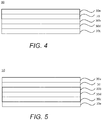
- FIGs. 2-5 illustrate various optical devices 10 contemplated herein. These are exemplary in nature. It should be appreciated that the order of the coatings on the first exposed side and the second unexposed side can vary. Additionally, the types of coatings present on the first exposed side and the second unexposed side can vary. Generally, the coatings 30 that can provide a mechanical or protective function are present on the first exposed side of the optical device and the coatings that can provide an optical function are present on the second exposed side of the optical device. The coatings 30 of FIGs. 2-5 are described more fully below.
- an optical device 10 including on a first exposed side an antireflective coating with anti-smudge treatment 30a, a substrate 20, and on a second unexposed side an electrical conducting coating 30b, and a glare reducing coating 30c.
- an optical device 10 including on a first exposed side an antireflective coating with anti-smudge treatment 30a, a substrate 20, and on a second unexposed side an electrical conducting coating 30b, a glare reducing coating 30c, and an antireflective coating 30e.
- an optical device 10 including on a first exposed side an antireflective coating with anti-smudge treatment 30a, a substrate 20, and on a second unexposed side an electrical conducting coating 30b, a bandpass filter 30d, and a glare reducing coating 30c.
- an optical device 10 including on a first exposed side an antireflective coating with anti-smudge treatment 30a, a substrate 20, and on a second unexposed side an electrical conducting coating 30b, a bandpass filter 30d, a glare reducing coating 30c, and an antireflective coating 30e.
- the optical device 10 can include a coating 30 applied to the substrate 20, such as an antireflective coating 30e.
- the antireflective coating 30e can be present on the first side of the optical device 10.
- the antireflective coating 30 can also be treated to confer an anti-smudge 30a property, as shown in FIGS. 2-5 .
- the antireflective coating 30e can be present on the second side of the optical device 10, as shown in FIGs. 3 and 6 .
- the optical device 10 can include an antireflective coating with an anti-smudge treatment 30a on a first side and an antireflective coating 30e (without an anti-smudge treatment) on the second side.
- An antireflective coating 30e can be a dielectric stack and can reduce the light reflection on an interface with the substrate 20.
- Suitable dielectrics for forming the dielectric stack include metal oxides such as TiO 2 , Ta 2 O 5 , ZrO 2 , and SiO 2 , which are optically isotropic and ca exhibit high transparency in the visible wavelength spectrum range (e.g., from 400nm to 700nm).
- the antireflective coating 30e can be a stack including a first plurality of dielectric layers having a first refractive index, such as a low refractive index, for example, SiO 2 or magnesium fluoride (MgF 2 ), interleaved with at least a second plurality of dielectric layers having a second refractive index, such as a high refractive index.
- first refractive index such as a low refractive index, for example, SiO 2 or magnesium fluoride (MgF 2
- MgF 2 magnesium fluoride
- high refractive index materials include niobium oxide, tantalum oxide, aluminum oxide, titanium oxide, zirconium oxide, and their combinations.
- the antireflective coating 30e can be formed of a stack of layers of NbTiO x , SiO 2 , or the like.
- the antireflective coating 30e can be a thin film dielectric stack of a first layer of NbTiO x of about 50 nm, a first layer of SiO 2 of about 18 nm, a second layer of NbTiO x of about 16 nm, a second layer of SiO 2 of about 101 nm.
- the optical device 10 can include a coating 30 applied to the substrate, such as a protectant coating.
- the protectant coating can be present on the first side of the optical device.
- the optical device 10 can include the protectant coating alone or in combination with the antireflective coating 30e.
- the protectant coating is applied to an antireflective coating 30e, which is applied to the substrate 20.
- the protectant coating and the antireflective coating 30e are both on the first side of the optical device 10.
- the protectant coating can include a fluorinated alkyl ether polymer having a functionalized silane.
- a fluorinated alkyl ether polymer having a functionalized silane has the general formula: R m -Si-X n (1), where R includes the fluorinated alkyl ether repeat unit, X can be an alkoxy group, a chloride, or an amine group, in which m + n equals 4.
- R m -Si-X n (1)
- R includes the fluorinated alkyl ether repeat unit
- X can be an alkoxy group, a chloride, or an amine group, in which m + n equals 4.
- poly(perfluoropropyl ether) functionalized with a tri-methoxy silane group and poly(perfluoroethyl ether) functionalized with a silazane group are two such compounds.
- a protectant coating can be durable and can include a compound having the simplified formula: CF 3 -[CH(CF 3 )-CH 2 -O-] x -CONCH 3 -(CH 2 ) 3 -Si-(OC 2 H 5 ) 3 (2), where x is an integer from 7-11.
- This compound can also include a divalent linking group (i.e., -CONCH 3 -(CH 2 ) 3 -).
- -CONCH 3 -(CH 2 ) 3 - compounds similar in structure and function to that shown in formula (2) can also be used in the protectant coating.
- both N-methyl-N-(-triethoxypropyl)-2-[a-heptafluoropropoxy ⁇ Poly(oxy(trifluoromethyl)-1,2-ethanediyl) ⁇ tetrafluoropropionamide, commercially available compounds, can be used in the protectant coating.
- Methods of applying the protectant coating can include wet techniques such as dipping, flowing, wiping, and/or spraying the surface with a liquid, solution, or gel-like carrier containing the coating compound, and dry techniques such as vapor coating the coating compound onto a surface (either at ambient pressure or under vacuum).
- the optical device 10 can include a coating 30 applied to the substrate 20, such as an electrical conducting coating 30b, as shown in FIGs. 2-5 .
- the electrical conducting coating 30b can be present on the second side of the optical device 10.
- the electrical conducting coating 30b can be a low surface energy treatment that serves as a soil, water, and dust repelling surface. This coating 30b can have a low coefficient of friction, such as less than 0.08. In this manner, the electrical conducting coating 30b can reduce the susceptibility of the optical device 10 to being damaged by an abrasive media.
- the electrical conducting coating 30b can include indium tin oxide (ITO), nano-particles based transparent composites, and other commonly used optically transparent conductors.
- ITO indium tin oxide
- the electrical conducting coating 30b can be transparent at a wavelength of operation of a LIDAR sensor, such as between about 850 nm to about 2000 nm.
- the electrical conducting coating 30b can act as a heating element to increase a temperature of the optical device 10, such as from about 30° C to 80° C.
- a heating element an optical device 10 including this coating 30b can be used to eliminate and/or reduce at least one of: the risk of fogging of a window with an attached sensor, risk of moisture condensation, and increase soil repellency of the first exposed side of the optical device 10.
- this electrical conducting coating 30b can increase the hydrophobicity and oleophobicity of an outer antireflective coating 30 on a first side of the substrate by increasing the efficiency in repelling water and contaminants.
- the electrical conducting coating 30b may not be mechanically durable enough to create a robust surface. For this reason, the electrically conducting coating 30b should be applied to the second side, i.e. the side of the optical device facing the sensor.
- the optical device 10 can include a coating 30 applied to the substrate 20, such as a glare reducing coating 30c.
- the glare reducing coating 30c can be present on the second unexposed side of the optical device 10, as shown in FIGs. 2-5 .
- the glare reducing coating 30c and an electrical conducting coating 30b can both be present on the second unexposed side of the optical device 10.
- the glare reducing coating 30c can be applied to an electrical conducting coating 30b, which is applied to the substrate 20.
- An example of a glare reducing coating 30c can be a multi-layer structure of a circular polarizer including a linear polarizer combined with a quarter wave optical retarder.
- Wave retarders are birefringent materials that alter (retard) the polarization state or phase of light traveling through them.
- a wave retarder has a fast (extraordinary) and slow (ordinary) axis. As polarized light passes through a wave retarder, the light passing through the fast axis travels more quickly through the wave retarder than through the slow axis.
- the wave plate retards the velocity of one of the polarization components (x or y) one quarter of a wave out of phase from the other polarization component.
- the glare reducing coating 30c can reduce and/or eliminate glare at the wavelength of operation of the sensor protected by the optical device 10.
- the glare reducing coating 30c can also allow for analysis of the polarization state of a signal beam.
- the optical device 10 can include a coating 30 applied to the substrate 20, such as a bandpass filter 30d.
- the bandpass filter 30d can be present on the second unexposed side of the optical device 10, as shown in FIGs. 4-5 .
- the bandpass filter 30d can be applied to the glare reducing coating 30c, which can be applied to an electrical conducting coating 30b, which is applied to the substrate 20.
- the bandpass filter 30d, glare reducing coating 30c, and the electrical conducting coating 30b can all be present on the second unexposed side of the optical device 10.
- the glare reducing coating 30c can be applied to an electrical conducting coating 30b, which is applied to the substrate 20.
- the bandpass filter 30d can be realized by a full stack of dielectric low and high refractive materials. Each layer can be deposited as a quarter-wave (QW) thickness at the wavelength of the desired filter. Each partial-reflector, which may be comprised of only a single layer, is called a quarter-wave stack (QWS). The bandwidth of the filter is a function of the reflectance of quarter-wave stacks in the structure. The center wavelength of the pass-band is determined by the thickness of the spacer dielectric material.
- the dielectric materials used for the quarter and/or half-wave layers have indices of refraction in the range 1.3 to beyond 4.0.
- some suitable materials are: Magnesium Fluoride (1.38), Thorium Fluoride (1.47), Cryolite (1.35), Silicon Dioxide (1.46), Aluminum Oxide (1.63), Hafnium Oxide (1.85), Tantalum Pentoxide (2.05), Niobium Oxide (2.19), Zinc Sulphide (2.27), Titanium Oxide (2.37), Silicon (3.5), Germanium (4.0), and Lead Telluride (5.0).
- Other dielectric materials would serve as well.
- the fully dielectric band pass filter 30d can also combine anti-reflective properties.
- the bandpass filter 30d can be a polymeric coating containing an appropriate mixture of dyes to create required absorbance or a combination of dielectric and polymeric structures.
- the bandpass filter 30d can allow a wavelength of light at which a sensor operates pass and can eliminate all other wavelengths.
- the bandpass filter 30d can block wavelengths in the visible and near IR spectral range, such as from about 400 to about 850 nm, and can transmit wavelengths above 850 nm. In this manner, the bandpass filter 30d can reduce and/or eliminate unwanted radiation from reaching a sensor attached to the optical device 10.
- the optical device 10 can be attached to another device to form an optical system.
- the other device can be a window, a sensor (e.g. LIDAR sensor), or a lens, for example, a self-standing optical lens, or a lens.
- the optical device 10 can be attached to the other device using conventional deposition processes.
- a method of making an optical device 10 is also disclosed.
- the optical device 10 can be formed using semiconductor processes.
- a method of making an optical system is also disclosed.
- the optical device 10 can be attached to another device by conventional deposition processes to form the optical system.
Landscapes
- Physics & Mathematics (AREA)
- General Physics & Mathematics (AREA)
- Optics & Photonics (AREA)
- Chemical & Material Sciences (AREA)
- Inorganic Chemistry (AREA)
- Surface Treatment Of Optical Elements (AREA)
- Optical Filters (AREA)
- Polarising Elements (AREA)
- Optical Head (AREA)
- Light Receiving Elements (AREA)
- Paints Or Removers (AREA)
- Surface Treatment Of Glass (AREA)
- Optical Elements Other Than Lenses (AREA)
- Glass Compositions (AREA)
- Laser Surgery Devices (AREA)
- Surgical Instruments (AREA)
Abstract
Description
- The present disclosure generally relates to an optical device including a substrate and a coating applied to the substrate, wherein the optical device has a first side exposed to an environment and a second side that is unexposed
- Optical devices for optical sensors are becoming increasingly important with the advent of semi-autonomous, autonomous, and remotely controlled vehicles. For example, there is an increase interest in the application of LIDAR (Light detection and ranging) technology in vehicles. However, the use of optical devices for optical sensors raises a concern as to whether the sensors can withstand mechanical, optical, and environmental factors that could damage or adversely impact the function of the sensors. As an example, the sensors would be subjected to environmental factors, such as rain and wind, that could damage, scratch, or otherwise effect the durability and operability of the sensor.
- In an aspect, there is disclosed an optical device comprising a substrate; and a coating applied to the substrate, wherein the optical device has a first side exposed to an environment and a second side that is unexposed.
- The substrate may include plastics, synthetic sapphire, glass and synthetic diamond.
- The optical device may include two or more substrates.
- The two or more substrates may be laminates.
- The coating may be an antireflective coating.
- The antireflective coating may be present on the first side of the optical device.
- The coating may be a protectant coating.
- The protectant coating may be applied to an antireflective coating, which may be applied to a substrate.
- Both the protectant coating and an antireflective coating may be on the first side of the optical device.
- The protectant coating may be present on the first side of the optical device.
- The coating may be an electrical conducting coating present on the second side of the optical device.
- The coating may be a glare reducing coating.
- The glare reducing coating may be applied to an electrical conducting coating, which may be applied to the substrate.
- Both the glare reducing coating and an electrical conducting coating may be on the second side of the optical device.
- The glare reducing coating may be present on the second side of the optical device.
- The coating may be a bandpass filter.
- The bandpass filter may be applied to glare reducing coating, which may be applied to an electrical conducting coating, which may be applied to a substrate.
- The bandpass filter, the glare reducing coating, and the electrical conducting coating may all be on the second side of the optical device.
- The bandpass filter may be present on the second side of the optical device.
- The coating may be an optical coating on the first side of the substrate and may include an AR coating, a protectant coating, a bandpass filter coating, and combination thereof.
- Additional features and advantages of various embodiments will be set forth, in part, in the description that follows, and will, in part, be apparent from the description, or may be learned by the practice of various embodiments. The objectives and other advantages of various embodiments will be realized and attained by means of the elements and combinations particularly pointed out in the description herein.
- The present disclosure in its several aspects and embodiments can be more fully understood from the detailed description and the accompanying drawings, wherein:
-
FIG. 1 is a cross-section of an optical device according to an aspect of the invention; -
FIG. 2 is a cross-section of an optical device according to another aspect of the invention; -
FIG. 3 is a cross-section of an optical device according to another aspect of the invention; -
FIG. 4 is a cross-section of an optical device according to another aspect of the invention; -
FIG. 5 is a cross-section of an optical device according to another aspect of the invention; and -
FIG. 6 is a cross-section of an optical device according to another aspect of the invention; - Throughout this specification and figures like reference numbers identify like elements.
- It is to be understood that both the foregoing general description and the following detailed description are exemplary and explanatory only, and are intended to provide an explanation of various embodiments of the present teachings. The layers/components shown in each Figure may be described with regard to a particular Figure, but it is understood that the description of a particular layer/component would be applicable to the equivalent layer/component in the other Figures.
- In its broad and varied embodiments, there is disclosed an
optical device 10 including asubstrate 20; and at least onecoating 30 applied to thesubstrate 20; in which theoptical device 10 has a first side exposed to an environment and a second side that is unexposed, as shown inFIG. 1 . An "exposed" first side means facing the environment, such as light, air, dirt, wind, etc. An "unexposed" second side means not facing the environment and can include being applied to another device, such as a window, a sensor (e.g. LIDAR sensor), or a lens, for example, a self-standing optical lens, or a lens as part of a complex optical system. - The disclosed
optical device 10 can include at least onecoating 30 that can protect another device, as disclosed above, against mechanical, optical, chemical and environmental factors. The at least onecoating 30 can provide at least one function. The at least onecoating 30 can include one or more coatings in order to provide multiple functions to theoptical device 10. Additionally, the at least onecoating 30 can include one ormore coatings 30 on an exposed first side and/or on an unexposed second side of thesubstrate 20 in order to optimize the functions of eachcoating 30 of theoptical device 10. - The
substrate 20 of theoptical device 10 can be any material capable of being coated. Non-limiting examples ofsubstrates 20 include plastics, synthetic sapphire, glass, synthetic diamond, optical ceramic materials, optical quality polymers, and light transmitting substrates with absorption spectra as required by the functional application of theoptical device 10, such as silicon. Optical quality polymers include polycarbonates, arcylates, and cyclic olefin polymers. Various types of glass can be used including chemically strengthened glass. - In an aspect, as shown in
FIG. 6 , theoptical device 100 can include more than onesubstrate substrate optical device 100 and the sensor it is applied thereon. Additionally, the inclusion of more than onesubstrate optical device 100 can increase the structural strength and/or flexibility of theoptical device 100. Theoptical device 100 can include two ormore substrates more substrates more substrates more substrates optical device 100. However, the thickness of a single substrate or a laminate substrate is not a limiting factor in selecting a substrate suitable for theoptical device 100. - The at least one
substrate first substrate 110a can be manufactured from hard optical materials ranging, depending on application and location, from chemically strengthened glass to inherently, extremely hard and impact resistant materials, such as synthetic sapphire or diamond. Thefirst substrate 110a can includecoatings 30 providing mechanical and protective functions on the first exposed side and can include a second substrate and/orcoatings 30 providing optical functions on the second unexposed side. Asecond substrate 110b can function as a carrier of optical coatings that can provide additional protective functions to theoptical device 10. - The substrate(s) 20, 110a, 110b, for use in the
optical device substrate optical device coatings 30 in theoptical device -
FIGs. 2-5 illustrate variousoptical devices 10 contemplated herein. These are exemplary in nature. It should be appreciated that the order of the coatings on the first exposed side and the second unexposed side can vary. Additionally, the types of coatings present on the first exposed side and the second unexposed side can vary. Generally, thecoatings 30 that can provide a mechanical or protective function are present on the first exposed side of the optical device and the coatings that can provide an optical function are present on the second exposed side of the optical device. Thecoatings 30 ofFIGs. 2-5 are described more fully below. - As shown in
FIG. 2 , there is illustrated anoptical device 10 including on a first exposed side an antireflective coating withanti-smudge treatment 30a, asubstrate 20, and on a second unexposed side anelectrical conducting coating 30b, and aglare reducing coating 30c. - As shown in
FIG. 3 , there is illustrated anoptical device 10 including on a first exposed side an antireflective coating withanti-smudge treatment 30a, asubstrate 20, and on a second unexposed side anelectrical conducting coating 30b, aglare reducing coating 30c, and anantireflective coating 30e. - As shown in
FIG. 4 , there is illustrated anoptical device 10 including on a first exposed side an antireflective coating withanti-smudge treatment 30a, asubstrate 20, and on a second unexposed side anelectrical conducting coating 30b, abandpass filter 30d, and aglare reducing coating 30c. - As shown in
FIG. 5 , there is illustrated anoptical device 10 including on a first exposed side an antireflective coating withanti-smudge treatment 30a, asubstrate 20, and on a second unexposed side anelectrical conducting coating 30b, abandpass filter 30d, aglare reducing coating 30c, and anantireflective coating 30e. - The
optical device 10 can include acoating 30 applied to thesubstrate 20, such as anantireflective coating 30e. In an aspect, theantireflective coating 30e can be present on the first side of theoptical device 10. Theantireflective coating 30 can also be treated to confer an anti-smudge 30a property, as shown inFIGS. 2-5 . In another aspect, theantireflective coating 30e can be present on the second side of theoptical device 10, as shown inFIGs. 3 and6 . Theoptical device 10 can include an antireflective coating with ananti-smudge treatment 30a on a first side and anantireflective coating 30e (without an anti-smudge treatment) on the second side. - An
antireflective coating 30e can be a dielectric stack and can reduce the light reflection on an interface with thesubstrate 20. Suitable dielectrics for forming the dielectric stack include metal oxides such as TiO2, Ta2O5, ZrO2, and SiO2, which are optically isotropic and ca exhibit high transparency in the visible wavelength spectrum range (e.g., from 400nm to 700nm). Theantireflective coating 30e can be a stack including a first plurality of dielectric layers having a first refractive index, such as a low refractive index, for example, SiO2 or magnesium fluoride (MgF2), interleaved with at least a second plurality of dielectric layers having a second refractive index, such as a high refractive index. Non-limiting examples of high refractive index materials include niobium oxide, tantalum oxide, aluminum oxide, titanium oxide, zirconium oxide, and their combinations. - The
antireflective coating 30e can be formed of a stack of layers of NbTiOx, SiO2, or the like. In an aspect, theantireflective coating 30e can be a thin film dielectric stack of a first layer of NbTiOx of about 50 nm, a first layer of SiO2 of about 18 nm, a second layer of NbTiOx of about 16 nm, a second layer of SiO2 of about 101 nm. - The
optical device 10 can include acoating 30 applied to the substrate, such as a protectant coating. The protectant coating can be present on the first side of the optical device. Theoptical device 10 can include the protectant coating alone or in combination with theantireflective coating 30e. In an aspect, the protectant coating is applied to anantireflective coating 30e, which is applied to thesubstrate 20. The protectant coating and theantireflective coating 30e are both on the first side of theoptical device 10. - In an aspect, the protectant coating can include a fluorinated alkyl ether polymer having a functionalized silane. An example of such a compound has the general formula: Rm-Si-Xn (1), where R includes the fluorinated alkyl ether repeat unit, X can be an alkoxy group, a chloride, or an amine group, in which m + n equals 4. For example, poly(perfluoropropyl ether) functionalized with a tri-methoxy silane group and poly(perfluoroethyl ether) functionalized with a silazane group, are two such compounds.
- A protectant coating can be durable and can include a compound having the simplified formula: CF3-[CH(CF3)-CH2-O-]x-CONCH3-(CH2)3-Si-(OC2H5)3 (2), where x is an integer from 7-11. This compound can also include a divalent linking group (i.e., -CONCH3-(CH2)3-). Of course, compounds similar in structure and function to that shown in formula (2) can also be used in the protectant coating. In particular, both N-methyl-N-(-triethoxypropyl)-2-[a-heptafluoropropoxy {Poly(oxy(trifluoromethyl)-1,2-ethanediyl)}tetrafluoropropionamide, commercially available compounds, can be used in the protectant coating.
- Methods of applying the protectant coating can include wet techniques such as dipping, flowing, wiping, and/or spraying the surface with a liquid, solution, or gel-like carrier containing the coating compound, and dry techniques such as vapor coating the coating compound onto a surface (either at ambient pressure or under vacuum).
- The
optical device 10 can include acoating 30 applied to thesubstrate 20, such as anelectrical conducting coating 30b, as shown inFIGs. 2-5 . Theelectrical conducting coating 30b can be present on the second side of theoptical device 10. Theelectrical conducting coating 30b can be a low surface energy treatment that serves as a soil, water, and dust repelling surface. Thiscoating 30b can have a low coefficient of friction, such as less than 0.08. In this manner, theelectrical conducting coating 30b can reduce the susceptibility of theoptical device 10 to being damaged by an abrasive media. - The
electrical conducting coating 30b can include indium tin oxide (ITO), nano-particles based transparent composites, and other commonly used optically transparent conductors. In an aspect, theelectrical conducting coating 30b can be transparent at a wavelength of operation of a LIDAR sensor, such as between about 850 nm to about 2000 nm. - The
electrical conducting coating 30b can act as a heating element to increase a temperature of theoptical device 10, such as from about 30° C to 80° C. As a heating element, anoptical device 10 including thiscoating 30b can be used to eliminate and/or reduce at least one of: the risk of fogging of a window with an attached sensor, risk of moisture condensation, and increase soil repellency of the first exposed side of theoptical device 10. - Additionally, this
electrical conducting coating 30b can increase the hydrophobicity and oleophobicity of an outerantireflective coating 30 on a first side of the substrate by increasing the efficiency in repelling water and contaminants. - The
electrical conducting coating 30b may not be mechanically durable enough to create a robust surface. For this reason, the electrically conductingcoating 30b should be applied to the second side, i.e. the side of the optical device facing the sensor. - The
optical device 10 can include acoating 30 applied to thesubstrate 20, such as aglare reducing coating 30c. Theglare reducing coating 30c can be present on the second unexposed side of theoptical device 10, as shown inFIGs. 2-5 . Theglare reducing coating 30c and anelectrical conducting coating 30b can both be present on the second unexposed side of theoptical device 10. In an aspect, theglare reducing coating 30c can be applied to anelectrical conducting coating 30b, which is applied to thesubstrate 20. - An example of a
glare reducing coating 30c can be a multi-layer structure of a circular polarizer including a linear polarizer combined with a quarter wave optical retarder. Wave retarders are birefringent materials that alter (retard) the polarization state or phase of light traveling through them. A wave retarder has a fast (extraordinary) and slow (ordinary) axis. As polarized light passes through a wave retarder, the light passing through the fast axis travels more quickly through the wave retarder than through the slow axis. In the case of a quarter wave retarder, the wave plate retards the velocity of one of the polarization components (x or y) one quarter of a wave out of phase from the other polarization component. Polarized light passing through a quarter wave retarder thus becomes circularly polarized. Theglare reducing coating 30c can reduce and/or eliminate glare at the wavelength of operation of the sensor protected by theoptical device 10. Theglare reducing coating 30c can also allow for analysis of the polarization state of a signal beam. - The
optical device 10 can include acoating 30 applied to thesubstrate 20, such as abandpass filter 30d. Thebandpass filter 30d can be present on the second unexposed side of theoptical device 10, as shown inFIGs. 4-5 . Thebandpass filter 30d can be applied to theglare reducing coating 30c, which can be applied to anelectrical conducting coating 30b, which is applied to thesubstrate 20. In an aspect, thebandpass filter 30d,glare reducing coating 30c, and theelectrical conducting coating 30b can all be present on the second unexposed side of theoptical device 10. In an aspect, theglare reducing coating 30c can be applied to anelectrical conducting coating 30b, which is applied to thesubstrate 20. - The
bandpass filter 30d can be realized by a full stack of dielectric low and high refractive materials. Each layer can be deposited as a quarter-wave (QW) thickness at the wavelength of the desired filter. Each partial-reflector, which may be comprised of only a single layer, is called a quarter-wave stack (QWS). The bandwidth of the filter is a function of the reflectance of quarter-wave stacks in the structure. The center wavelength of the pass-band is determined by the thickness of the spacer dielectric material. The dielectric materials used for the quarter and/or half-wave layers have indices of refraction in the range 1.3 to beyond 4.0. For example, some suitable materials are: Magnesium Fluoride (1.38), Thorium Fluoride (1.47), Cryolite (1.35), Silicon Dioxide (1.46), Aluminum Oxide (1.63), Hafnium Oxide (1.85), Tantalum Pentoxide (2.05), Niobium Oxide (2.19), Zinc Sulphide (2.27), Titanium Oxide (2.37), Silicon (3.5), Germanium (4.0), and Lead Telluride (5.0). Other dielectric materials would serve as well. Besides that, the fully dielectricband pass filter 30d can also combine anti-reflective properties. - In an aspect, the
bandpass filter 30d can be a polymeric coating containing an appropriate mixture of dyes to create required absorbance or a combination of dielectric and polymeric structures. - The
bandpass filter 30d can allow a wavelength of light at which a sensor operates pass and can eliminate all other wavelengths. For example, thebandpass filter 30d can block wavelengths in the visible and near IR spectral range, such as from about 400 to about 850 nm, and can transmit wavelengths above 850 nm. In this manner, thebandpass filter 30d can reduce and/or eliminate unwanted radiation from reaching a sensor attached to theoptical device 10. - The
optical device 10 can be attached to another device to form an optical system. The other device can be a window, a sensor (e.g. LIDAR sensor), or a lens, for example, a self-standing optical lens, or a lens. Theoptical device 10 can be attached to the other device using conventional deposition processes. - A method of making an
optical device 10 is also disclosed. Theoptical device 10 can be formed using semiconductor processes. - A method of making an optical system is also disclosed. The
optical device 10 can be attached to another device by conventional deposition processes to form the optical system. - From the foregoing description, those skilled in the art can appreciate that the present teachings can be implemented in a variety of forms. Therefore, while these teachings have been described in connection with particular embodiments and examples thereof, the true scope of the present teachings should not be so limited. Various changes and modifications may be made without departing from the scope of the teachings herein.
- This scope disclosure is to be broadly construed. It is intended that this disclosure disclose equivalents, means, systems and methods to achieve the devices, activities and mechanical actions disclosed herein. For each device, article, method, mean, mechanical element or mechanism disclosed, it is intended that this disclosure also encompass in its disclosure and teaches equivalents, means, systems and methods for practicing the many aspects, mechanisms and devices disclosed herein. Additionally, this disclosure regards a coating and its many aspects, features and elements. Such a device can be dynamic in its use and operation, this disclosure is intended to encompass the equivalents, means, systems and methods of the use of the device and/or article of manufacture and its many aspects consistent with the description and spirit of the operations and functions disclosed herein. The claims of this application are likewise to be broadly construed.
- The description of the inventions herein in their many embodiments is merely exemplary in nature and, thus, variations that do not depart from the gist of the invention are intended to be within the scope of the invention. Such variations are not to be regarded as a departure from the spirit and scope of the invention.
Claims (15)
- An optical device, comprising:a substrate; anda coating applied to the substrate,wherein the optical device has a first side exposed to an environment and a second side that is unexposed.
- The optical device of claim 1, wherein the substrate includes plastics, synthetic sapphire, glass and synthetic diamond.
- The optical device of claim 1, wherein the optical device includes two or more substrates.
- The optical device of claim 3, wherein the two or more substrates are laminates.
- The optical device of claim 1, wherein the coating is an antireflective coating.
- The optical device of claim 5, wherein the antireflective coating is present on the first side of the optical device.
- The optical device of claim 1, wherein the coating is a protectant coating.
- The optical device of claim 7, wherein the protectant coating is applied to an antireflective coating, which is applied to the substrate.
- The optical device of claim 7, wherein the protectant coating and an antireflective coating are both on the first side of the optical device.
- The optical device of claim 8, wherein the protectant coating is present on the first side of the optical device.
- The optical device of claim 1, wherein the coating is an electrical conducting coating present on the second side of the optical device.
- The optical device of claim 1, wherein the coating is glare reducing coating and is applied to an electrical conducting coating, which is applied to the substrate.
- The optical device of claim 12, wherein the glare reducing coating and an electrical conducting coating are both on the second side of the optical device.
- The optical device of claim 1, wherein the coating is a bandpass filter present on the second side of the optical device.
- The optical device of claim 14, wherein the bandpass filter is applied to a glare reducing coating, which is applied to an electrical conducting coating, which is applied to a substrate.
Priority Applications (1)
| Application Number | Priority Date | Filing Date | Title |
|---|---|---|---|
| EP21192023.6A EP3951444B1 (en) | 2018-01-30 | 2019-01-24 | Optical device having optical and mechanical properties |
Applications Claiming Priority (1)
| Application Number | Priority Date | Filing Date | Title |
|---|---|---|---|
| US201862624009P | 2018-01-30 | 2018-01-30 |
Related Child Applications (2)
| Application Number | Title | Priority Date | Filing Date |
|---|---|---|---|
| EP21192023.6A Division EP3951444B1 (en) | 2018-01-30 | 2019-01-24 | Optical device having optical and mechanical properties |
| EP21192023.6A Previously-Filed-Application EP3951444B1 (en) | 2018-01-30 | 2019-01-24 | Optical device having optical and mechanical properties |
Publications (2)
| Publication Number | Publication Date |
|---|---|
| EP3518006A2 true EP3518006A2 (en) | 2019-07-31 |
| EP3518006A3 EP3518006A3 (en) | 2019-10-09 |
Family
ID=65241124
Family Applications (2)
| Application Number | Title | Priority Date | Filing Date |
|---|---|---|---|
| EP19153602.8A Withdrawn EP3518006A3 (en) | 2018-01-30 | 2019-01-24 | Optical device having optical and mechanical properties |
| EP21192023.6A Active EP3951444B1 (en) | 2018-01-30 | 2019-01-24 | Optical device having optical and mechanical properties |
Family Applications After (1)
| Application Number | Title | Priority Date | Filing Date |
|---|---|---|---|
| EP21192023.6A Active EP3951444B1 (en) | 2018-01-30 | 2019-01-24 | Optical device having optical and mechanical properties |
Country Status (8)
| Country | Link |
|---|---|
| US (3) | US11360242B2 (en) |
| EP (2) | EP3518006A3 (en) |
| JP (4) | JP2019133153A (en) |
| KR (1) | KR20190092302A (en) |
| CN (2) | CN110095828A (en) |
| CA (2) | CA3031650C (en) |
| MX (2) | MX2023000863A (en) |
| TW (2) | TWI785189B (en) |
Cited By (1)
| Publication number | Priority date | Publication date | Assignee | Title |
|---|---|---|---|---|
| WO2022150095A1 (en) * | 2021-01-05 | 2022-07-14 | Ppg Industries Ohio, Inc. | Coated articles demonstrating anti-reflection, contaminant build-up resistance and uv durability |
Families Citing this family (5)
| Publication number | Priority date | Publication date | Assignee | Title |
|---|---|---|---|---|
| EP3999868A2 (en) * | 2019-07-19 | 2022-05-25 | Innoviz Technologies Ltd. | Antireflective sticker for lidar window |
| CN112526478A (en) * | 2019-11-22 | 2021-03-19 | 宁波舜宇车载光学技术有限公司 | Composite protection device and manufacturing method thereof, outer cover and laser radar device |
| US12578519B2 (en) | 2020-03-05 | 2026-03-17 | Viavi Solutions Inc. | Optical coating for organic surface treatments |
| TWI895581B (en) * | 2021-02-02 | 2025-09-01 | 瑞士商羅立克科技股份公司 | Method for manufacturing a spatially limited film stack comprising at least one optically anisotropic film on a light sensor element of an optical sensor device, electronic device, use of the electronic device and use of the electronic device in a display setup |
| CN113933922A (en) * | 2021-10-22 | 2022-01-14 | 中国科学院光电技术研究所 | Ultrathin composite material diffraction lens for high-resolution imaging and preparation method thereof |
Citations (2)
| Publication number | Priority date | Publication date | Assignee | Title |
|---|---|---|---|---|
| WO2013151984A2 (en) * | 2012-04-02 | 2013-10-10 | Guardian Industries Corp. | Heatable lens for luminaires, and/or methods of making the same |
| WO2017145910A1 (en) * | 2016-02-23 | 2017-08-31 | 東海光学株式会社 | Nd filter with plastic base material, and nd filter with plastic base material for eyeglasses |
Family Cites Families (55)
| Publication number | Priority date | Publication date | Assignee | Title |
|---|---|---|---|---|
| US4747674A (en) * | 1986-04-18 | 1988-05-31 | Polaroid Corporation | Contrast enhancement filter |
| JPH0738788A (en) | 1993-07-22 | 1995-02-07 | Sharp Corp | Camera monitoring device |
| JPH09230031A (en) * | 1995-12-22 | 1997-09-05 | Toto Ltd | Inter-vehicle distance detection device and vehicle equipped with the same |
| TW446637B (en) * | 1996-05-28 | 2001-07-21 | Mitsui Chemicals Inc | Transparent laminates and optical filters for displays using the same |
| US7351470B2 (en) * | 1998-02-19 | 2008-04-01 | 3M Innovative Properties Company | Removable antireflection film |
| US6800378B2 (en) * | 1998-02-19 | 2004-10-05 | 3M Innovative Properties Company | Antireflection films for use with displays |
| DE19956089A1 (en) * | 1999-11-22 | 2001-06-21 | Bayerische Motoren Werke Ag | Sensor arrangement |
| JP2002071940A (en) * | 2000-08-25 | 2002-03-12 | Fuji Photo Film Co Ltd | Optical filter, front plate using the same, and image display device |
| US7954719B2 (en) * | 2000-11-24 | 2011-06-07 | Metrologic Instruments, Inc. | Tunnel-type digital imaging-based self-checkout system for use in retail point-of-sale environments |
| JP4683747B2 (en) * | 2001-03-05 | 2011-05-18 | 大日本印刷株式会社 | Antistatic antiglare film |
| JP4627610B2 (en) * | 2001-06-19 | 2011-02-09 | 株式会社ファルテック | Infrared sensor cover and infrared sensor unit using the same |
| JP4117173B2 (en) * | 2002-09-26 | 2008-07-16 | 富士フイルム株式会社 | Production method of retardation plate and retardation plate produced by the method |
| JP2004198617A (en) * | 2002-12-17 | 2004-07-15 | Nissan Motor Co Ltd | Infrared transmitting film, infrared sensor cover and infrared sensor unit using the same |
| CN100442090C (en) * | 2003-01-24 | 2008-12-10 | 日东电工株式会社 | Color Correcting Polarizers |
| JP2005199572A (en) * | 2004-01-16 | 2005-07-28 | Nitto Denko Corp | Antifouling type antireflection film and display device |
| JP2006194639A (en) * | 2005-01-11 | 2006-07-27 | Denso Corp | Radar equipment |
| US20060204766A1 (en) * | 2005-03-14 | 2006-09-14 | Jds Uniphase Corporation | Anti-moisture and soil-repellent coatings |
| CN100565248C (en) * | 2007-03-29 | 2009-12-02 | 郭爱军 | New anti-reflective conductive film |
| JP2008268277A (en) * | 2007-04-16 | 2008-11-06 | Sei Hybrid Kk | Infrared ray transmitting structure and infrared ray sensor |
| JP2009054902A (en) * | 2007-08-29 | 2009-03-12 | Canon Inc | Display device |
| US20090104438A1 (en) * | 2007-10-17 | 2009-04-23 | Jennifer Hoyt Lalli | Abrasion resistant coatings |
| TW200933238A (en) * | 2008-01-28 | 2009-08-01 | Delta Electronics Inc | Touch panel |
| US8830141B2 (en) * | 2009-04-02 | 2014-09-09 | GM Global Technology Operations LLC | Full-windshield head-up display enhancement: anti-reflective glass hard coat |
| WO2011017039A2 (en) * | 2009-08-03 | 2011-02-10 | 3M Innovative Properties Company | Antireflective transparent emi shielding optical filter |
| US8939606B2 (en) * | 2010-02-26 | 2015-01-27 | Guardian Industries Corp. | Heatable lens for luminaires, and/or methods of making the same |
| US8834976B2 (en) * | 2010-02-26 | 2014-09-16 | Guardian Industries Corp. | Articles including anticondensation and/or low-E coatings and/or methods of making the same |
| BR112014009556A2 (en) * | 2011-10-20 | 2017-06-13 | Oakley, Inc | glasses, laminates and their methods of making them |
| EP2605043B1 (en) | 2011-12-15 | 2014-07-23 | Upwind | A self-cleaning light detection and ranging device |
| DE102011122345A1 (en) * | 2011-12-23 | 2013-06-27 | Valeo Schalter Und Sensoren Gmbh | Optical measuring device and method for producing a cover for a housing of an optical measuring device |
| JP2013156523A (en) * | 2012-01-31 | 2013-08-15 | Topcon Corp | Substrate |
| WO2013143615A1 (en) * | 2012-03-30 | 2013-10-03 | Applied Materials, Inc. | Transparent body for use in a touch panel and its manufacturing method and apparatus |
| WO2013169987A1 (en) * | 2012-05-10 | 2013-11-14 | Oakley, Inc. | Eyewear with laminated functional layers |
| TW201403831A (en) * | 2012-07-12 | 2014-01-16 | Pixart Imaging Inc | Optical device with embedded non-lens transparent package |
| TWI684031B (en) * | 2012-07-16 | 2020-02-01 | 美商唯亞威方案公司 | Optical filter and sensor system |
| JP6144548B2 (en) | 2012-08-01 | 2017-06-07 | 日東電工株式会社 | Transparent conductive laminated film, method for producing the same, and touch panel |
| EP2903823B1 (en) * | 2012-10-03 | 2021-09-22 | Corning Incorporated | Surface-modified glass substrate |
| JP6257897B2 (en) * | 2013-01-30 | 2018-01-10 | イーエイチエス レンズ フィリピン インク | Optical article and manufacturing method thereof |
| JP2015040945A (en) | 2013-08-21 | 2015-03-02 | コニカミノルタ株式会社 | In-vehicle camera lens unit |
| WO2015101584A1 (en) * | 2013-12-31 | 2015-07-09 | Essilor International (Compagnie Generale D'optique) | Multi-layer assembly and method for controlling layer thicknesses |
| WO2015134609A1 (en) * | 2014-03-05 | 2015-09-11 | 5.11, Inc. | Tactical circular polarized eyewear |
| US9933632B2 (en) * | 2014-03-26 | 2018-04-03 | Indizen Optical Technologies, S.L. | Eyewear lens production by multi-layer additive techniques |
| KR102397527B1 (en) * | 2014-07-08 | 2022-05-13 | 바스프 에스이 | Detector for determining a position of at least one object |
| KR101611208B1 (en) | 2014-11-05 | 2016-04-11 | 주식회사 엘엠에스 | Optical filter for solid-state image pickup device, and image pickup device containing the same |
| WO2016129699A1 (en) * | 2015-02-13 | 2016-08-18 | 日本板硝子株式会社 | Windshield |
| JP6513486B2 (en) * | 2015-05-27 | 2019-05-15 | ジオマテック株式会社 | Antifogging antireflective film, cover substrate with antifogging antireflective film, and method for producing antifogging antireflective film |
| EP3182158B1 (en) * | 2015-12-18 | 2021-11-24 | STMicroelectronics (Research & Development) Limited | Ranging apparatus |
| US9923007B2 (en) * | 2015-12-29 | 2018-03-20 | Viavi Solutions Inc. | Metal mirror based multispectral filter array |
| US10170509B2 (en) * | 2016-02-12 | 2019-01-01 | Viavi Solutions Inc. | Optical filter array |
| JP6431864B2 (en) | 2016-03-25 | 2018-11-28 | 株式会社ファルテック | Radar cover |
| EP3447521B1 (en) * | 2016-04-20 | 2019-12-18 | Konica Minolta, Inc. | Laser sensor and method for manufacturing exterior component |
| US11306392B2 (en) * | 2016-06-07 | 2022-04-19 | Nitto Denko Corporation | Method for producing optical film |
| CA3027712A1 (en) * | 2016-06-13 | 2017-12-21 | Viavi Solutions Inc. | Protected item including a protective coating |
| US11137519B2 (en) * | 2016-07-21 | 2021-10-05 | Rosemount Aerospace Inc. | Multi-fiber optical sensor for icing |
| JP2018031888A (en) * | 2016-08-24 | 2018-03-01 | 豊田合成株式会社 | Near infrared sensor cover |
| WO2018052057A1 (en) * | 2016-09-15 | 2018-03-22 | 豊田合成 株式会社 | Near infrared sensor cover |
-
2019
- 2019-01-21 MX MX2023000863A patent/MX2023000863A/en unknown
- 2019-01-21 MX MX2019000869A patent/MX2019000869A/en unknown
- 2019-01-21 TW TW108102235A patent/TWI785189B/en active
- 2019-01-21 TW TW111140490A patent/TWI906558B/en active
- 2019-01-24 EP EP19153602.8A patent/EP3518006A3/en not_active Withdrawn
- 2019-01-24 EP EP21192023.6A patent/EP3951444B1/en active Active
- 2019-01-25 JP JP2019011620A patent/JP2019133153A/en active Pending
- 2019-01-25 CA CA3031650A patent/CA3031650C/en active Active
- 2019-01-25 CA CA3190326A patent/CA3190326A1/en active Pending
- 2019-01-25 CN CN201910075164.3A patent/CN110095828A/en active Pending
- 2019-01-25 CN CN202410368565.9A patent/CN118011534A/en active Pending
- 2019-01-29 KR KR1020190011039A patent/KR20190092302A/en not_active Ceased
- 2019-01-29 US US16/261,189 patent/US11360242B2/en active Active
-
2021
- 2021-05-25 JP JP2021087644A patent/JP7268086B2/en active Active
-
2022
- 2022-05-31 US US17/828,978 patent/US12174342B2/en active Active
-
2023
- 2023-04-20 JP JP2023069146A patent/JP2023100706A/en active Pending
-
2024
- 2024-11-28 JP JP2024207001A patent/JP2025028999A/en active Pending
- 2024-12-23 US US19/000,123 patent/US20250123425A1/en active Pending
Patent Citations (3)
| Publication number | Priority date | Publication date | Assignee | Title |
|---|---|---|---|---|
| WO2013151984A2 (en) * | 2012-04-02 | 2013-10-10 | Guardian Industries Corp. | Heatable lens for luminaires, and/or methods of making the same |
| WO2017145910A1 (en) * | 2016-02-23 | 2017-08-31 | 東海光学株式会社 | Nd filter with plastic base material, and nd filter with plastic base material for eyeglasses |
| EP3407100A1 (en) * | 2016-02-23 | 2018-11-28 | Tokai Optical Co., Ltd. | Nd filter with plastic base material, and nd filter with plastic base material for eyeglasses |
Cited By (2)
| Publication number | Priority date | Publication date | Assignee | Title |
|---|---|---|---|---|
| WO2022150095A1 (en) * | 2021-01-05 | 2022-07-14 | Ppg Industries Ohio, Inc. | Coated articles demonstrating anti-reflection, contaminant build-up resistance and uv durability |
| US12638615B2 (en) | 2021-01-05 | 2026-05-26 | Ppg Industries Ohio, Inc. | Coated articles demonstrating anti-reflection, contaminant build-up resistance and UV durability |
Also Published As
| Publication number | Publication date |
|---|---|
| JP2023100706A (en) | 2023-07-19 |
| EP3951444A1 (en) | 2022-02-09 |
| CA3031650A1 (en) | 2019-07-30 |
| MX2023000863A (en) | 2023-03-01 |
| KR20190092302A (en) | 2019-08-07 |
| MX2019000869A (en) | 2019-12-19 |
| US20220291423A1 (en) | 2022-09-15 |
| JP2021177240A (en) | 2021-11-11 |
| EP3951444B1 (en) | 2025-10-01 |
| CN118011534A (en) | 2024-05-10 |
| TW202307471A (en) | 2023-02-16 |
| EP3518006A3 (en) | 2019-10-09 |
| TWI785189B (en) | 2022-12-01 |
| JP2019133153A (en) | 2019-08-08 |
| US20190235135A1 (en) | 2019-08-01 |
| US20250123425A1 (en) | 2025-04-17 |
| US12174342B2 (en) | 2024-12-24 |
| CA3190326A1 (en) | 2019-07-30 |
| TWI906558B (en) | 2025-12-01 |
| JP7268086B2 (en) | 2023-05-02 |
| US11360242B2 (en) | 2022-06-14 |
| JP2025028999A (en) | 2025-03-05 |
| CN110095828A (en) | 2019-08-06 |
| CA3031650C (en) | 2023-04-11 |
| TW201932876A (en) | 2019-08-16 |
Similar Documents
| Publication | Publication Date | Title |
|---|---|---|
| US12174342B2 (en) | Optical device having optical and mechanical properties | |
| EP3540478A2 (en) | Optical device including stack of optical layers with functional treatment | |
| JP5741283B2 (en) | Infrared light transmission filter and imaging apparatus using the same | |
| EP4431271A1 (en) | Windshield and windshield assembly | |
| CN111936896A (en) | Filters and Information Acquisition Devices | |
| CN116669943A (en) | Coated articles exhibiting anti-reflection, anti-stain build-up and UV durability | |
| JP2003248102A (en) | Multi-layer anti-reflection coating | |
| WO2024048254A1 (en) | Light absorbing composition, light absorber, optical filter, environmental light sensor, imaging device, method for producing light absorbing composition, and method for producing light absorber | |
| WO2006117979A1 (en) | Infrared blocking filter | |
| HK40010054A (en) | Optical device having optical and mechanical properties | |
| US12578519B2 (en) | Optical coating for organic surface treatments | |
| HK40103759A (en) | Optical device having optical and mechanical properties | |
| CN118050841A (en) | Optical filters and covers for LiDAR sensors | |
| WO2026000535A1 (en) | Display film material and preparation method therefor | |
| HK40006362A (en) | Optical device including stack of optical layers with functional treatment | |
| HK40011468A (en) | Optical device including stack of optical layers with functional treatment | |
| KR20160067058A (en) | Optical filter for image pickup device, and image pickup device containing the same |
Legal Events
| Date | Code | Title | Description |
|---|---|---|---|
| PUAI | Public reference made under article 153(3) epc to a published international application that has entered the european phase |
Free format text: ORIGINAL CODE: 0009012 |
|
| STAA | Information on the status of an ep patent application or granted ep patent |
Free format text: STATUS: THE APPLICATION HAS BEEN PUBLISHED |
|
| AK | Designated contracting states |
Kind code of ref document: A2 Designated state(s): AL AT BE BG CH CY CZ DE DK EE ES FI FR GB GR HR HU IE IS IT LI LT LU LV MC MK MT NL NO PL PT RO RS SE SI SK SM TR |
|
| AX | Request for extension of the european patent |
Extension state: BA ME |
|
| PUAL | Search report despatched |
Free format text: ORIGINAL CODE: 0009013 |
|
| AK | Designated contracting states |
Kind code of ref document: A3 Designated state(s): AL AT BE BG CH CY CZ DE DK EE ES FI FR GB GR HR HU IE IS IT LI LT LU LV MC MK MT NL NO PL PT RO RS SE SI SK SM TR |
|
| AX | Request for extension of the european patent |
Extension state: BA ME |
|
| RIC1 | Information provided on ipc code assigned before grant |
Ipc: G01S 7/481 20060101ALI20190830BHEP Ipc: G02B 5/08 20060101ALI20190830BHEP Ipc: G02B 5/28 20060101ALI20190830BHEP Ipc: G02B 1/14 20150101ALI20190830BHEP Ipc: G02B 1/115 20150101ALI20190830BHEP Ipc: G02B 1/16 20150101ALI20190830BHEP Ipc: G02B 1/08 20060101AFI20190830BHEP |
|
| STAA | Information on the status of an ep patent application or granted ep patent |
Free format text: STATUS: REQUEST FOR EXAMINATION WAS MADE |
|
| 17P | Request for examination filed |
Effective date: 20200409 |
|
| RBV | Designated contracting states (corrected) |
Designated state(s): AL AT BE BG CH CY CZ DE DK EE ES FI FR GB GR HR HU IE IS IT LI LT LU LV MC MK MT NL NO PL PT RO RS SE SI SK SM TR |
|
| STAA | Information on the status of an ep patent application or granted ep patent |
Free format text: STATUS: EXAMINATION IS IN PROGRESS |
|
| 17Q | First examination report despatched |
Effective date: 20200703 |
|
| STAA | Information on the status of an ep patent application or granted ep patent |
Free format text: STATUS: THE APPLICATION IS DEEMED TO BE WITHDRAWN |
|
| 18D | Application deemed to be withdrawn |
Effective date: 20210819 |