EP3514592B1 - System für faseroptische kommunikationsverbindungen - Google Patents
System für faseroptische kommunikationsverbindungen Download PDFInfo
- Publication number
- EP3514592B1 EP3514592B1 EP18213300.9A EP18213300A EP3514592B1 EP 3514592 B1 EP3514592 B1 EP 3514592B1 EP 18213300 A EP18213300 A EP 18213300A EP 3514592 B1 EP3514592 B1 EP 3514592B1
- Authority
- EP
- European Patent Office
- Prior art keywords
- port
- fiber optic
- circuitry
- optic cable
- connector
- Prior art date
- Legal status (The legal status is an assumption and is not a legal conclusion. Google has not performed a legal analysis and makes no representation as to the accuracy of the status listed.)
- Active
Links
Images



Classifications
-
- G—PHYSICS
- G02—OPTICS
- G02B—OPTICAL ELEMENTS, SYSTEMS OR APPARATUS
- G02B6/00—Light guides; Structural details of arrangements comprising light guides and other optical elements, e.g. couplings
- G02B6/24—Coupling light guides
- G02B6/42—Coupling light guides with opto-electronic elements
- G02B6/4201—Packages, e.g. shape, construction, internal or external details
- G02B6/4274—Electrical aspects
- G02B6/4284—Electrical aspects of optical modules with disconnectable electrical connectors
-
- G—PHYSICS
- G02—OPTICS
- G02B—OPTICAL ELEMENTS, SYSTEMS OR APPARATUS
- G02B6/00—Light guides; Structural details of arrangements comprising light guides and other optical elements, e.g. couplings
- G02B6/24—Coupling light guides
- G02B6/42—Coupling light guides with opto-electronic elements
- G02B6/4201—Packages, e.g. shape, construction, internal or external details
- G02B6/4204—Packages, e.g. shape, construction, internal or external details the coupling comprising intermediate optical elements, e.g. lenses, holograms
-
- G—PHYSICS
- G02—OPTICS
- G02B—OPTICAL ELEMENTS, SYSTEMS OR APPARATUS
- G02B6/00—Light guides; Structural details of arrangements comprising light guides and other optical elements, e.g. couplings
- G02B6/24—Coupling light guides
- G02B6/42—Coupling light guides with opto-electronic elements
- G02B6/4292—Coupling light guides with opto-electronic elements the light guide being disconnectable from the opto-electronic element, e.g. mutually self aligning arrangements
-
- G—PHYSICS
- G02—OPTICS
- G02B—OPTICAL ELEMENTS, SYSTEMS OR APPARATUS
- G02B6/00—Light guides; Structural details of arrangements comprising light guides and other optical elements, e.g. couplings
- G02B6/24—Coupling light guides
- G02B6/42—Coupling light guides with opto-electronic elements
- G02B6/4295—Coupling light guides with opto-electronic elements coupling with semiconductor devices activated by light through the light guide, e.g. thyristors, phototransistors
-
- G—PHYSICS
- G02—OPTICS
- G02B—OPTICAL ELEMENTS, SYSTEMS OR APPARATUS
- G02B6/00—Light guides; Structural details of arrangements comprising light guides and other optical elements, e.g. couplings
- G02B6/44—Mechanical structures for providing tensile strength and external protection for fibres, e.g. optical transmission cables
- G02B6/4439—Auxiliary devices
- G02B6/4471—Terminating devices ; Cable clamps
-
- G—PHYSICS
- G02—OPTICS
- G02B—OPTICAL ELEMENTS, SYSTEMS OR APPARATUS
- G02B6/00—Light guides; Structural details of arrangements comprising light guides and other optical elements, e.g. couplings
- G02B6/24—Coupling light guides
- G02B6/42—Coupling light guides with opto-electronic elements
- G02B6/4292—Coupling light guides with opto-electronic elements the light guide being disconnectable from the opto-electronic element, e.g. mutually self aligning arrangements
- G02B6/4293—Coupling light guides with opto-electronic elements the light guide being disconnectable from the opto-electronic element, e.g. mutually self aligning arrangements hybrid electrical and optical connections for transmitting electrical and optical signals
Definitions
- This disclosure relates to fiber optic communication and, in particular, to communication connections for fiber optic communication.
- Fiber optic communication may occur using optical fiber to transmit data in the form of light.
- the light provides a carrier wave, which can be modulated to represent the data.
- Optical fiber can develop signal transmission issues if the light signal is somehow compromised. Degradation in a fiber optic signal may be a result of contamination of optical connector interfaces, poor polishing of a ferrule assembly, damage to optical connectors, defective interconnections or splicing, or excessive bending of the optical fiber.
- Optical fiber is typically bundled in a fiber optic cable having an outer protective cover or cladding.
- an adapter assembly includes a single-piece or two-piece multi-fiber adapter defining a recess at which a contact assembly is disposed.
- the adapter assemblies can be disposed within adapter block assemblies or cassettes, which can be mounted to moveable trays. Both ports of the adapters disposed within adapter block assemblies are accessible. Only one port of each adapter disposed within the cassettes are accessible. Circuit boards can be mounted within the block assemblies or cassettes to provide communication between the contact assemblies and a data network.
- Japanese patent application JP 2012/168443 A discloses a photoelectric conversion device with a connector and a method for manufacturing photoelectric conversion device with connector.
- the photoelectric conversion device has a circuit board, a photoelectric conversion element mounted on the circuit board, an optical fiber optically connected to the photoelectric conversion element, connector units electrically connected to the circuit board and used for connection with an external device.
- United States patent application US 2011/229089 A1 discloses small-form-factor fiber optic interface assemblies for electronic devices.
- the fiber optic interface assemblies include a receptacle configured to matingly engage with a plug of a fiber optic cable assembly.
- the assemblies can support both optical and electrical communication and functionality.
- United States patent application US 2011/033190 A1 discloses a digital data harness that uses a signal specific conditioning circuit to interface with analog sensors. Signal specific conditioning circuits convert data signals from analog to digital and thereby allow signals to be transmitted over a digital data harness.
- the optical harness assembly includes at least one optical harness cable having a termination end; at least one electrical connector having connector pins; and at least one active connector conversion unit coupled between the termination end of the optical harness cable and the electrical connector.
- the present disclosure provides a system for fiber-optic communication as claimed in claim 1.
- Optional features are included in the dependent claims.
- a system for fiber optic communication connections includes a housing, a circuit board disposed in the housing and a port included in the housing.
- the port forms an opening in the housing that is configured to receive a fiber optic cable.
- the system includes a fiber optic cable comprising printed circuitry printed on an outer surface of the fiber optic cable, the printed circuitry being configured to convert optical signals transmitted by the cable to electrical signals.
- Circuitry included in the port is positioned for electrical communication with printed circuitry on the fiber optic cable when the fiber optic cable is received in the port.
- the system includes a keyway in the port to axially and rotationally align the fibre optic cable so that the printed circuitry aligns with the circuitry included in the port.
- the port includes a locking stay configured to fixedly couple and hold the fiber optic cable in place in the port.
- the system also includes an output connector configured for detachable connection and output of electrical signals, the output connector being in electrical communication with the circuitry included in the port.
- the system also has a connector configured to couple with an end of the fiber optic cable and sized to be received and mated with the locking stay.
- An interesting feature of the system described herein relates to interface circuitry included in the system that is aligned to electrically communicate with the printed circuitry included on the fiber optic cable due to predetermined axial and rotational orientation of the fiber optic cable in the port.
- the connector includes a cavity formed to receive, lock in place and provide a liquid-tight seal between the exterior surface of the fiber optic cable and the connector.
- the connector is formed to be received, lock in place and provide a liquid-tight seal with the port.
- the connector includes interface circuitry that is aligned with printed circuitry on the fiber optic cable and with interface circuitry included in the port. Alignment may be created by allowing ingress of the fiber optic cable into the connector in only a predetermined orientation and ingress of the connector into the port in only a predetermined orientation to complete an electrical communication path.
- Another interesting feature of the system relates to the configuration of the port to directly receive the fiber optic cable in only a predetermined orientation such that printed circuitry on the fiber optic cable is aligned with interface circuitry in the port, the fiber optic cable is locked in the port to resist egress, and a liquid-tight seal is formed between the fiber optic cable and the port.
- system may be configured to form a seal between an outer surface of the connector and the opening in the housing to prevent an end of the fiber optic cable received in the port from fluid communication external to the port.
- the locking stay is configured to allow the connector ingress to a predetermined distance into the port.
- the locking stay is configured to prevent egress of the connector from the port.
- the opening in the port accessible by the connector and the fiber optic cable from outside the housing, and the locking stay is disposed in the opening in the port to receive the connector and the fiber optic cable inserted into the opening.
- the connector is sized for receipt by the port and comprises an interface to electrically couple the printed circuitry with the circuitry included in the port.
- the connector comprises an enclosure having an interior wall and an exterior wall, the interior wall configured to receive the fiber optic cable and resist against egress, and the exterior wall sized for receipt in the locking stay and including a detent to bias the connector against removal from the locking stay.
- the port forms an opening in the connector housing, and the port is further configured to form a liquid-tight seal between the port and the fiber optic cable.
- the port further comprises a locking ring, the locking ring configured to receive the fiber optic cable and restrict egress of the fiber optic cable from the port.
- a converter is configured to convert between the light signal and an electrical signal, and an amplifier to amplify the electrical signal after conversion from a light signal.
- system further comprises a transducer configured to receive and decode digital data transmitted via the fiber optic cable to generate an analog electrical signal representative of the digital data.
- the circuitry included in the port includes interface circuitry that is aligned to electrically communicate with the printed circuitry included on the fiber optic cable due to the predetermined rotational orientation.
- the port is mounted on a printed circuit board, the printed circuit board comprising circuitry configured to process signals received from the fiber optic cable, or a copper cable.
- the printed circuitry comprises a photo diode in electrical communication with the circuitry in the port.
- system further comprises signal output circuitry in electrical communication with the transducer, the signal output circuitry configured to amplify and output the analog electrical signal to an output connector configured for detachable connection and operable to output the analog electrical signal.
- the keyway included in the port is configured to correspond to a slot formed in a cladding of the fiber optic cable, and the locking stay is configured to enable ingress and restrict egress of the fiber optic cable.
- the keyway included in the port is a first coupler configured to fixedly mate with a second coupler, the second coupler configured to fixedly couple with the fiber optic cable and align with the keyway included in the port so that egress of the fiber optic cable is restricted.
- the second coupler includes an interface to provide electrical communication between the printed circuitry included on the fiber optic cable and the circuity included in the port.
- Another interesting feature of the system is the capability to be self-powered and have energy storage capability using light signals.
- the system can receive external power or supply external power in different applications via the output connector.
- the system may be used in applications such as gas turbine engines as detachable connectors that convert between electrical signals and optical signals for efficient and electrically isolated communications between components.
- the system prevents contamination of the fiber optic communication path and efficiently and compactly converts electrical signals to optical signals by creating a sealed conversion environment with aligned electrical communication pathways.
- the system provides a locking capability that prevents repeated exposure of the optical communication pathway to contaminants while the system's output connector still allows detachable connection and disconnection of the communication pathways for maintenance and service of equipment.
- FIG. 1 illustrates a block diagram of an example of a system for fiber optic communication connections 100.
- the system 100 includes a housing 102, a circuit board 104 disposed in the housing 102, a port 106 forming an opening 108 in the housing 102.
- the opening 108 is formed to receive a fiber optic cable 110 from outside the housing 102.
- the system 100 includes circuitry 114, to receive and process digital data transmitted via the fiber optic cable 110.
- the circuitry 114 may include interface circuitry 116, transducer circuitry 118, light channel circuitry 120 and energy storage circuitry 122.
- the system 100 may perform conversion between electrical signals and optical signals for signals received from and provided to the fiber optic cable 110.
- system 100 may process electrical signals received from and provided to other signal transmission mechanisms such as wired or wireless transmission paths.
- system 100 may provide a detachable fiber optic termination that operates as an electrical conversion network using photovoltaic elements such as photodiodes or other elements for signal conversion.
- the housing 102 may be any form of rigid structure, such as plastic, having a cavity in which at least the circuit board 104, the port 106, and the circuitry may be disposed.
- the housing 102 may be an environmentally sealed enclosure that provides a liquid-tight barrier for a cavity included in the housing.
- the housing 102 may be formed and sized to be a connector housing suitable for mounting at the end of the fiber optic cable 110.
- the circuit board 104 may be any form of circuit structure, such as a printed circuit board (PCB), disposed within the cavity in the housing and providing a platform for electrical communication of at least some of the circuitry 114.
- PCB printed circuit board
- the port 106 includes a locking stay 126 that is disposed in the opening 108 and receives and fixedly holds the connector 200 in place.
- the fiber optic cable 110 may be friction fit within the locking stay 126.
- the locking stay 126 may include barbs, a roughened surface, a woven sleeve (finger puzzle), a push-to-connect fitting, or any other form of coupling that allows ingress, but not egress of the fiber optic cable 110.
- the locking stay 126 may allow the fiber optic cable 110 ingress to a predetermined distance into the port 106. Once the fiber optic cable 110 is inserted through the opening 108 into the port 106, the locking stay 126 may prevent egress of the fiber optic cable 110 from the port 106.
- the port 106 may form a seal between an outer surface of the fiber optic cable 110 and the opening 108 in the housing 102 to prevent an end of the fiber optic cable 110 that is received in the port 106 from fluid communication external to the port 106.
- the seal that is formed may eliminate contamination from entering the port 106 after the fiber optic cable 110 is inserted.
- Fiber optic systems with interconnections between segments of the network may develop signal transmission issues (signal amplitude and fidelity), such as after the connection has been opened and closed.
- Signal transmission issues signal amplitude and fidelity
- causes for this signal degradation are typically associated with: 1. Contamination of the optical connector interface, 2. Poor polishing of the ferrule assembly, 3. Damage to the optical connectors, 4. Defective interconnections or splicing, 5. Excessive bending of the fiber optic cable.
- the contamination of the optical connector interface is one of the largest complaints and problems with the disassembly and reassembly of the communication path.
- the port 106 may not only provide a seal against such contamination once the fiber optic cable 110 is inserted, but also prevent egress of the fiber optic cable, thereby eliminating the fiber optic communication path being opened and closed repeatedly.
- the system includes an output connector to detachable connect the system with external devices or systems during installation, maintenance and the like.
- Initial and one time insertion of the fiber optic cable 110 into the port 106 to create the optical communication path may be performed in a clean environment, such as a manufacturing clean room following cleaning and polishing in order to effectively complete the optical communication path interconnection.
- initial one-time insertion of the fiber optic cable 110 into the port 106 to effectively complete the optical communication path interconnection may be performed in a manufacturing or repair environment before or after the fiber optic cable has been routed.
- the fiber optic cable 110 may be received directly into the opening 108 of the port 106 to effectively complete the optical communication path interconnection.
- a connector may be coupled with the end of the fiber optic cable 110, and the locking stay 126 may be sized to receive and mate with the connector during the one time insertion into the port 106 to effectively complete the optical communication path interconnection.
- FIG. 2 is a perspective view of an example connector 200.
- the connector 200 may be formed of a rigid material, such as plastic, and includes a barrel 202 formed to be received as a one-time insertion into the port 106 ( FIG. 1 ), and an outer seal 204 formed to provide a seal when mated with the port 106.
- the connector 200 is formed to include a cavity 206 sized to receive as a one-time insertion an end of a fiber optic cable 110.
- the cavity 206 and the fiber optic cable 110 may be concentrically aligned with a centerline 210 of the connector 200.
- the barrel 202 includes an interior wall 212 and an exterior wall 214.
- the interior wall 212 may include an electrical interface 216, which may be positioned in the interior wall 212 to electrically couple with printed circuitry 218 included on the fiber optic cable 110.
- the printed circuitry 218 and the interface 216 may be aligned and electrically coupled when the fiber optic cable 110 is inserted into the cavity 206 to effectively complete the optical communication path interconnection.
- the interface 216 may be in any location in the interior wall 212, and printed circuitry 218 may correspondingly located in any location on the surface of the fiber optic cable 110.
- the exterior wall 214 of the connector 200 may include a slot 220.
- the slot 220 may be sized to receive a keyway included in the port 106 ( FIG. 1 ) so as to axially and rotationally align the fiber optic cable 110 in the port 106.
- the slot 220 may be formed as a predetermined shape in the barrel 202.
- the slot 220 is formed as a rectangular shape void to extend a predetermined depth into the barrel 202 and a predetermined length along the barrel 202.
- the slot 220 may be any other configuration or shape so long as it performs a rotational and axial alignment function.
- FIG. 3 is an end view of the example connector 200 of FIG. 2 .
- the slot 220 extends a predetermined distance into the barrel 202, which may limit the axial progress of the barrel 202 into the port.
- the interface 216 extends perpendicular to the centerline 210 away from the interior surface 212 of the connector 200 to the exterior surface 214 so as to provide electrical communication between the printed circuitry 218 and circuitry included in the port 106 ( FIG. 1 ).
- the interface 216 may be any form of electrically conductive material, such as copper or aluminum.
- the slot 220 may align with the keyway 126 ( FIG.
- FIG. 4 is a cut-away side view of the example connector 200 illustrated in FIG. 3 .
- the outer seal 204 is illustrated to include a sloped surface 302 and a detent 304.
- the sloped surface 302 may be a conical surface have a predetermined slope that may equal and opposite to a predetermined slope included in the locking stay 126 of the port 106.
- the detent 304 may be a rigid member that fixedly engages a portion of the port 106.
- the locking stay 126 may fixedly engage the detent 304, and the sloped surface 302 may contiguously engage with the port to form a liquid-tight seal between the connector 200 and the port 106.
- the outer seal 204 may be any other form or sealing mechanism, and may include for example, a gasket, an o-ring, an adhesive, or any other mechanism to create a liquid-tight seal.
- the term "liquid-tight seal” refers to any mechanism or combination of mechanisms that can operate to stop liquid communication past the seal and thereby exclude contaminants from optical connector interface.
- the detent 304 may allow one-time ingress of the barrel 202 into the port 106 and cooperatively operate with the locking stay 126 to resist egress of the connector 200 out of the port 106.
- the port 106 may also, or alternatively, include a detent to engage the connector 200.
- the fiber optic cable 110 may be inserted as a one-time installation into the cavity 206 in the barrel 202 so as to engage fingers 304 included in the cavity 206.
- the fingers 304 may be positioned on or near the interior wall 212 of the connector 200 so that the cavity 206 can receive the fiber optic cable 110 and resist against egress using the fingers 304.
- the interior wall 212 may be configured to receive the fiber optic cable 110 and resist against egress
- the exterior wall 214 may be sized to be received in the locking stay 126 and the detent 302 may bias the connector against removal from the locking stay 126.
- the fingers 304 may fixedly hold an outer surface, such as a cladding of the fiber optic cable 110, such as by piercing and engaging the outer surface.
- the fingers 304 may be barbs, a roughened surface, a woven sleeve (finger puzzle), a push-to-connect fitting, a friction fit, or any other form of coupling that allows ingress, but not egress of the fiber optic cable 110.
- the slot 220 may engage a keyway included in the port 106 such that one-time ingress of the connector 200 containing the fiber optic cable 110 is restricted to a predetermined rotational orientation.
- the keyway included in the port 106 may be a first coupler that is fixedly and permanently mated with a second coupler in the form of the connector 200, where the connector 200 is fixedly coupled with the fiber optic cable in a predetermined rotational and axial alignment and with the port 106 in a predetermined rotational and axial alignment.
- the connector 200 may be omitted, the outer surface of the fiber optic cable 110 may include a slot that corresponds to a keyway included in the port 106, and the locking stay 126 may enable ingress and restrict egress of the fiber optic cable 110 to create a one-time mating.
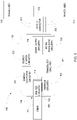
- FIG. 5 is a block diagram of an example of the system 100.
- the system 100 includes an output connector 502 that may have signal channels 504 in electrical communication with signal lines 506, and also may optionally have power channels 508 in electrical communication with power lines 510 for supply of AC or DC power to or from the system 100.
- the output connector 502 may be any form of detachable connection mechanism to couple the system 100 to the signal lines 506 and optionally to the power lines 510.
- the output connector 502 may be formed of a rigid material, such as plastic, and may be a male or a female coupler that corresponds to a coupler on a piece of equipment external to the system 100.
- the power channels 506 and/or the signal channels 504 may be pins or an edge connector disposed in a coupler housing in predetermined positions to allow detachable coupling with a corresponding coupler housing only when the couplers are in a predetermined alignment.
- the output connector 502 may extend from the housing 102 and may receive and output the output signals during operation of the system 100, and may receive and supply input signals to the system 100.
- the housing 102 includes signal output circuitry 516, signal processing circuitry 518, transducer circuitry 520, and interface circuitry 522 used in the communication path between the output connector 502 and the fiber optic cable 110. All or some of this circuitry may be mounted on a circuit board included in the housing 102. In addition, the housing 102 may optionally include energy collection circuitry 526 and energy storage circuitry 528.
- the circuitry is hardware, and may include one or more processors and memory storing instructions executable by the processor(s), and data.
- the circuitry may also include components such as resistors, capacitors, inductors, diodes, transistors, amplifiers and the like as, well as devices capable of executing logic, such as logic devices, microprocessor(s), field programmable gate arrays, and the like.
- the fiber optic cable 110 includes printed circuitry 218 that is inserted into the port 106 to create the fiber optic communication pathway.
- the printed circuitry in 218 may include, p-n Photodiode(s), pin Photodetector(s), Schottky Barrier Photodetector, Metal Photodetector, Photoconductive Detector, Phototransistor, Avalanche Photodetector, or the like. In other examples, fewer or greater numbers of blocks may be used to illustrate the functionality described herein.
- the printed circuitry 218 may include photovoltaic components and communication paths in the form of optical processing circuitry to convert between data in the form of light signals and data in the form of electrical signals.
- the printed circuitry 218 is physically printed on an outer surface of the fiber optic cable 110.
- the printed circuitry 218 may include an optical transmitter configured to transmit and receive lights signals, along with other optical signal components, to convert between digital data transmitted via the fiber optic cable 110 in the form of light signals and electrical signals such as analog or digital electrical signals.
- the printed circuitry may include an amplifier used as part of the conversion between digital data transmitted via the fiber optic cable 110 in the form of light signals and electrical signals such as analog or digital electrical signals. The amplifier may amplify the electrical signals.
- the printed circuitry 218 may include a photo diode 530 that reacts electrically to the presence and absence of light signals, and electrical contacts 532 that can be axially and rotationally aligned with electrical contacts 532 included in the interface circuitry 522.
- the interface circuitry 522 may be positioned and aligned to electrically communicate with the printed circuitry 218.
- the interface circuitry 522 may be included in the connector 200, and also in the port 106 with contacts 532 to provide electrical communication pathways. Alternatively, the interface circuitry 522 may be entirely included in the port 106 with contacts 532 to interface with the printed circuitry 218.
- the interface circuitry 522 may operate as a communication path between the printed circuitry 218 and the functionality included in the system 100. Thus, the interface circuitry 522 may receive digital data transmitted via the fiber optic cable, which is provided via the printed circuitry 218.
- the interface circuitry 522 may provide for signal conversion, signal amplification of the electrical signals via an amplifier included in the interface circuitry 522, error checking, lost data packet recovery/administration and other communication and network related functionality. Further, portions of the photovoltaic components included in the optical processing circuitry that are not included in the printed circuitry 218 may be included in the interface circuitry 522.
- the interface 522 may include or entirely be printed circuitry included in the housing 102.
- the transducer circuitry 520 may receive and decode digital electrical signal data and generate analog electrical signals representative of the digital data.
- the term "electrical signals" refers to an electrical communication represented by voltage and/or current that is provided in a conductor such as a wire or bus.
- the transducer circuitry 520 may receive and encode analog electrical signals and generate a digital electrical signal data, representative of the analog electrical signals.
- Digital data may be received from the printed circuitry 218 via the interface circuitry 522 and passed to the signal processing circuitry 520 as analog signals, and analog data may be received from the signal processing circuitry 518 and passed to the interface circuitry 522 as digital data.
- the transducer circuitry 520 may also include portions of the optical processing circuitry.
- the interface 522 or the transducer circuitry 520 may include an amplifier to amplify the electrical signals.
- the printed circuitry 218 and the interface circuitry 522 may include, p-n Photodiode(s), pin Photodetector(s), Schottky Barrier Photodetector, Metal Photodetector, Photoconductive Detector, Phototransistor, Avalanche Photodetector, or the like.
- the transducer circuitry 520 may sense optical one's and zero's for sampling and may be included in the printed circuitry 218 or in the housing 102. In another example, the transducer circuitry 520 may be mounted on and connected with the circuit board 104 ( FIG. 1 ).
- the signal processing circuitry 518 may include ancillary electronics such as signal scaling and conversion, amplification, attenuation, and other forms of signal manipulation functionality, such as opto-isolators, filters and any other signal processing related items.
- the signal processing circuitry 518 may include signal amplification circuitry for the analog electrical signals being communicated.
- the signal output circuitry 516 may output signals on the signal channels 504 to the signals lines 506.
- the signal output circuitry 516 may output analog electrical signals generated from converted light signals received over the fiber optic cable 110.
- the signal output circuitry 516 may include communication protocol conditioning, filtering, multiplexing and other forms of signal transmission techniques.
- the output signals/data may be processed to support ETHERNET, CAN, RS232, RS485 or other types of communication protocols.
- the circuitry included in the system may be supplied AC or DC power via the power lines 510 as input power, which is received over the power channels 508.
- the power channels 508 may supply auxiliary power to one or more power buses included in the circuit board 104 included in the housing 102 to, for example, perform signal amplification using the signal processing circuitry 518.
- the power channels 508 may supply power as output power to the power lines 510. Such output power may be supplied by the cooperative operation of the energy collection circuitry 526 and the energy storage circuitry 528.
- the energy collection circuitry 526 may include a photo electric cell to capture the incident light provided by the fiber optic cable 110.
- the energy collection circuitry 526 may also include processing circuitry to convert the light received by the photo electric cell to electrical power.
- the electrical power may be used to operate the circuitry in the system 100.
- the power may also be stored in the energy storage circuitry 528.
- the energy storage circuitry 528 may include an energy storage device, such as one or more batteries and/or capacitors and a charging/discharging control system for the energy storage device.
- the energy storage circuitry 528 may be selectively used to supply AC or DC power to circuitry in the system 100, such as the signal output circuitry 516, signal processing circuitry 518, transducer circuitry 520, and interface circuitry 522 at times when the power generated from the incident light is insufficient to meet the load demands of the system 100.
- the energy collection circuitry 526 and the energy storage circuitry 528 may also cooperative operate to selectively supply output power on the power channels 508 to supply the power lines 510 thereby supply power to devices external to the system 100.
- FIG. 6 is an example implementation of a first system 602 and a second system 604 in an example implementation, such as a gas turbine engine 600.
- the first system 602 and the second system 604 may be provided as detachable connectors or couplers at opposite ends of a piece of fiber optic cable 110 that is, for example one to twenty meters in length.
- the first system 602 may have its output connector 502 detachably mated with a control unit 608, and the second system 604 have its output connector 502 detachably mated with a node 610, such as one or more sensors or control nodes.
- the output connectors 502 may supply and receive electrical signals between the control unit 608 and node 610.
- the fiber optic cable 110 may provide an interconnecting fiber optic communication link and may be terminated and fixedly held in the port of each of the first system 602 and the second system 604 in a sealed condition.
- the first system 602 and the second system 604 may provide conversion between optical signals transmitted on the fiber optic cable 110 and the electrical signals at the output connectors 502.
- these optical to electrical signal conversion interconnections allow signal and power to flow between the control unit 608 and the node 610.
- the first system 602 and the second system 604 are readily detachable from the control unit 608 and the node 610, respectively, without compromise or contamination of the optical communication pathway.
- control unit 608 may be a Full Authority Digital Engine Control (FADEC) or Electronic Control Unit (ECU) of a gas turbine engine.
- the interconnecting fiber optic cable 110 may be routed around the engine to the node 610.
- the fiber optic cable 110 may be of sufficient heat resistance to handle the high temperatures present in a gas turbine engine compartment.
- the node 610 may be, for example, a smart sensor that is powered by the control unit via the fiber optic cable 110 and the power channels included in the first system 602 and the second system 604. In this example, despite repeated connection and disconnection, in a gas turbine engine environment, of the first system 602 and the second system 604 , from the control unit 608 and the node 610, respectively, the fiber optic communication path remains contaminant free.
- the system 100 may be implemented with additional, different, or fewer components.
- the system 100 may include only the printed circuitry 218, signal processing circuitry 518 and the output connector 502.
- the system 100 may include only the printed circuitry 218, the interface circuitry 522 and the signal output circuitry 516.
- Each component may include additional, different, or fewer components.
- the printed circuitry 218 may include the transducer circuitry 520 in some examples.
- the signal output circuitry 516 and the signal processing circuitry 518 may be combined.
- each circuitry such as the signal output circuitry 516, signal processing circuitry 518, transducer circuitry 520, and interface circuitry 522, may be hardware or a combination of hardware and software.
- each circuitry may include an application specific integrated circuit (ASIC), a Field Programmable Gate Array (FPGA), a circuit, a digital logic circuit, an analog circuit, a combination of discrete circuits, gates, or any other type of hardware or combination thereof.
- ASIC application specific integrated circuit
- FPGA Field Programmable Gate Array
- each circuitry may include memory hardware, such as a portion of a memory, for example, that comprises instructions executable with a processor to implement one or more of the features of the circuitry.
- each circuitry may or may not include the processor.
- each circuitry may just be the portion of the memory that comprises instructions executable with a processor to implement the features of the corresponding circuitry without the circuitry including any other hardware. Because each circuitry includes at least some hardware even when the included hardware comprises software, each circuitry may be interchangeably referred to as a hardware module.
- the respective logic, software or instructions for implementing the processes, methods and/or techniques discussed above may be provided on computer readable storage media.
- the functions, acts or tasks illustrated in the figures or described herein may be executed in response to one or more sets of logic or instructions stored in or on computer readable media.
- the functions, acts or tasks are independent of the particular type of instructions set, storage media, processor or processing strategy and may be performed by software, hardware, integrated circuits, firmware, micro code and the like, operating alone or in combination.
- processing strategies may include multiprocessing, multitasking, parallel processing and the like.
- the instructions are stored on a removable media device for reading by local or remote systems.
- the logic or instructions are stored in a remote location for transfer through a computer network or over telephone lines.
- the logic or instructions are stored within a given computer, central processing unit (“CPU”), graphics processing unit (“GPU”), or system.
- a second action may be said to be "in response to" a first action independent of whether the second action results directly or indirectly from the first action.
- the second action may occur at a substantially later time than the first action and still be in response to the first action.
- the second action may be said to be in response to the first action even if intervening actions take place between the first action and the second action, and even if one or more of the intervening actions directly cause the second action to be performed.
- a second action may be in response to a first action if the first action includes setting a Boolean variable to true and the second action is initiated if the Boolean variable is true.
- the phrases "at least one of ⁇ A>, ⁇ B>, ... and ⁇ N>” or “at least one of ⁇ A>, ⁇ B>, ... ⁇ N>, or combinations thereof" or " ⁇ A>, ⁇ B>, ... and/or ⁇ N>” are defined by the Applicant in the broadest sense within the scope of the appended claims, superseding any other implied definitions hereinbefore or hereinafter unless expressly asserted by the Applicant to the contrary, to mean one or more elements selected from the group comprising A, B, ... and N.
- the phrases mean any combination of one or more of the elements A, B, ... or N including any one element alone or the one element in combination with one or more of the other elements which may also include, in combination, additional elements not listed, within the scope of the appended claims.
Landscapes
- Physics & Mathematics (AREA)
- General Physics & Mathematics (AREA)
- Optics & Photonics (AREA)
- Optical Couplings Of Light Guides (AREA)
- Connector Housings Or Holding Contact Members (AREA)
Claims (14)
- System (100) für faseroptische Kommunikation, umfassend:ein Gehäuse (102);eine in dem Gehäuse angeordnete Leiterplatte (104);einen Anschluss (106), der in dem Gehäuse eingeschlossen ist, wobei der Anschluss eine Öffnung (108) in dem Gehäuse bildet, die dazu konfiguriert ist, ein faseroptisches Kabel (110) aufzunehmen;ein faseroptisches Kabel (110), das eine gedruckte Schaltung (218) umfasst, die auf eine Außenfläche des faseroptischen Kabels gedruckt ist, wobei die gedruckte Schaltung dazu konfiguriert ist, optische Signale, die durch das Kabel übertragen werden, in elektrische Signale umzuwandeln;eine Schaltung (114, 116, 118, 120, 122), die in dem Anschluss eingeschlossen ist, wobei die Schaltung zur elektrischen Kommunikation mit der gedruckten Schaltung (218) an dem faseroptischen Kabel positioniert ist, wenn das faseroptische Kabel in dem Anschluss aufgenommen ist;eine in dem Anschluss eingeschlossene Keilnut zum axialen und drehbaren Ausrichten des faseroptischen Kabels, sodass die gedruckte Schaltung (218) mit der in dem Anschluss eingeschlossenen Schaltung (114, 116, 118, 120, 122) ausgerichtet ist;eine Verriegelungsstrebe (126), die an dem Anschluss eingeschlossen ist, wobei die Verriegelungsstrebe dazu konfiguriert ist, das faseroptische Kabel fest mit dem Anschluss koppelt und an Ort und Stelle zu halten;einen Ausgangsverbinder (502), der für eine lösbare Verbindung und Ausgabe von elektrischen Signalen konfiguriert ist, wobei der Ausgangsverbinder in elektrischer Kommunikation mit der Schaltung (114, 116, 118, 120, 122) steht, die in dem Anschluss eingeschlossen ist; undeinen Verbinder (200), der dazu konfiguriert ist, mit einem Ende des faseroptischen Kabels gekoppelt zu werden, und dazu bemessen ist, mit der Verriegelungsstrebe (126) aufgenommen und zusammengepasst zu werden.
- System nach Anspruch 1, wobei der Anschluss (106) dazu konfiguriert ist, eine Dichtung zwischen einer Außenfläche des Verbinders (200) und der Öffnung in dem Gehäuse zu bilden, um zu verhindern, dass ein Ende des faseroptischen Kabels (110) von der Fluidkommunikation außerhalb des Anschlusses in dem Anschluss aufgenommen wird.
- System nach Anspruch 1 oder 2, wobei die Verriegelungsstrebe (126) dazu konfiguriert ist, dem Verbinder (200) einen Eintritt bis zu einer vorbestimmten Entfernung in den Anschluss (106) zu ermöglichen; und/oder die Verriegelungsstrebe dazu konfiguriert ist, einen Austritt des Verbinders aus dem Anschluss zu verhindern.
- System nach einem der vorhergehenden Ansprüche, wobei die Öffnung (108) in dem Anschluss (106) durch den Verbinder (200) und das faseroptische Kabel (110) von außerhalb des Gehäuses (102) zugänglich ist und die Verriegelungsstrebe (126) in der Öffnung in dem Anschluss angeordnet ist, um den Verbinder und das in die Öffnung eingeführte faseroptische Kabel aufzunehmen.
- System nach Anspruch 1, wobei der Verbinder (200) für die Aufnahme durch den Anschluss (106) bemessen ist und eine Schnittstelle umfasst, um die gedruckte Schaltung (218) elektrisch mit der in dem Anschluss eingeschlossene Schaltung zu koppeln.
- System nach Anspruch 5, wobei der Verbinder (200) eine Umhüllung mit einer Innenwand (212) und einer Außenwand (214) umfasst, wobei die Innenwand dazu konfiguriert ist, das faseroptische Kabel (110) aufzunehmen und einem Austritt zu widerstehen, und die Außenwand für eine Aufnahme in der Verriegelungsstrebe (126) bemessen ist und eine Arretierung einschließt, um den Verbinder gegen ein Entfernen von der Verriegelungsstrebe vorzuspannen.
- System nach einem der vorhergehenden Ansprüche, ferner umfassend einen Wandler, der dazu konfiguriert ist, digitale Daten zu empfangen und zu decodieren, die über das faseroptische Kabel übertragen werden, um ein analoges elektrisches Signal zu generieren, das die digitalen Daten darstellt.
- System nach Anspruch 7, wobei die in dem Anschluss (106) eingeschlossene Schaltung eine Schnittstellenschaltung (116, 522) einschließt, die ausgerichtet ist, um aufgrund der vorbestimmten Drehausrichtung elektrisch mit der an dem faseroptischen Kabel (110) eingeschlossenen gedruckten Schaltung (218) zu kommunizieren.
- System nach Anspruch 7 oder 8, wobei der Anschluss (106) an einer gedruckten Leiterplatine montiert ist, wobei die gedruckte Leiterplatine eine Schaltung umfasst, die dazu konfiguriert ist, Signale zu verarbeiten, die von dem faseroptischen Kabel (110) oder einem Kupferkabel empfangen werden.
- System nach Anspruch 8 oder 9, wobei die gedruckte Schaltung (218) eine Fotodiode (530) in elektrischer Kommunikation mit der Schaltung in dem Anschluss (106) umfasst.
- System nach einem der Ansprüche 7 bis 10, ferner umfassend eine Signalausgangsschaltung (516) in elektrischer Kommunikation mit dem Wandler, wobei die Signalausgangsschaltung dazu konfiguriert ist, das analoge elektrische Signal zu verstärken und an den Ausgangsverbinder auszugeben.
- System nach einem der Ansprüche 7 bis 11, wobei die in dem Anschluss (106) eingeschlossene Keilnut dazu konfiguriert ist, einem Schlitz (220) zu entsprechend, der in einer Ummantelung des faseroptischen Kabels (110) gebildet ist, und die Verriegelungsstrebe (126) dazu konfiguriert ist, einen Eintritt des faseroptischen Kabels zu ermöglichen und einen Austritt davon einzuschränken.
- System nach einem der Ansprüche 7 bis 11, wobei die in dem Anschluss (106) eingeschlossene Keilnut ein erster Koppler ist, der dazu konfiguriert ist, fest mit einem zweiten Koppler zusammenpassen, wobei der zweite Koppler dazu konfiguriert ist, fest mit dem faseroptischen Kabel (110) gekoppelt und mit der in dem Anschluss eingeschlossenen Keilnut ausgerichtet zu werden, sodass ein Austritt des faseroptischen Kabels eingeschränkt ist.
- System nach Anspruch 13, wobei der zweite Koppler eine Schnittstelle einschließt, um eine elektrische Kommunikation zwischen der gedruckten Schaltung, die an dem faseroptischen Kabel (110) eingeschlossen ist, und der Schaltung, die in dem Anschluss (106) eingeschlossen ist, bereitzustellen.
Applications Claiming Priority (2)
| Application Number | Priority Date | Filing Date | Title |
|---|---|---|---|
| US201862618630P | 2018-01-18 | 2018-01-18 | |
| US16/125,396 US10451826B2 (en) | 2018-01-18 | 2018-09-07 | System for fiber optic communication connections |
Publications (2)
| Publication Number | Publication Date |
|---|---|
| EP3514592A1 EP3514592A1 (de) | 2019-07-24 |
| EP3514592B1 true EP3514592B1 (de) | 2023-02-01 |
Family
ID=64744562
Family Applications (1)
| Application Number | Title | Priority Date | Filing Date |
|---|---|---|---|
| EP18213300.9A Active EP3514592B1 (de) | 2018-01-18 | 2018-12-18 | System für faseroptische kommunikationsverbindungen |
Country Status (3)
| Country | Link |
|---|---|
| US (1) | US10451826B2 (de) |
| EP (1) | EP3514592B1 (de) |
| CA (1) | CA3027409A1 (de) |
Families Citing this family (2)
| Publication number | Priority date | Publication date | Assignee | Title |
|---|---|---|---|---|
| CN114077020A (zh) * | 2020-08-18 | 2022-02-22 | 华为技术有限公司 | 复合模块及其制造方法 |
| US12487425B2 (en) | 2023-03-21 | 2025-12-02 | Rtx Corporation | Coupling optical fibers and cooling fluid passages |
Family Cites Families (21)
| Publication number | Priority date | Publication date | Assignee | Title |
|---|---|---|---|---|
| US3792284A (en) | 1972-10-13 | 1974-02-12 | Gte Sylvania Inc | Electro-optic transmission link |
| US4186999A (en) | 1977-10-25 | 1980-02-05 | Amp Incorporated | Connector ferrule for terminating optical fiber cables |
| FR2435057A1 (fr) | 1978-09-01 | 1980-03-28 | Thomson Csf | Connecteur optique pour carte de circuit imprime |
| JPS58136009A (ja) | 1982-02-08 | 1983-08-12 | Sumitomo Electric Ind Ltd | 光フアイバ用水中コネクタ装置 |
| US4547039A (en) | 1982-04-16 | 1985-10-15 | Amp Incorporated | Housing mountable on printed circuit board to interconnect fiber optic connectors |
| US4597631A (en) | 1982-12-02 | 1986-07-01 | The United States Of America As Represented By The Secretary Of The Navy | Printed circuit card hybrid |
| US6246819B1 (en) | 1998-12-11 | 2001-06-12 | Prc Inc. | Fiber optic cladding displacement connector |
| US20040052471A1 (en) * | 2002-09-13 | 2004-03-18 | Fitel Usa Corp. | Connector systems for dynamically updating information related to a network and methods for developing the connector systems |
| US6973243B2 (en) * | 2003-02-13 | 2005-12-06 | Fujikura Ltd. | Cable |
| US20040184746A1 (en) | 2003-03-17 | 2004-09-23 | Chang Chin L. | Fiber optic connector extension for transmission of digital video data |
| JP4705432B2 (ja) | 2005-03-28 | 2011-06-22 | 富士通コンポーネント株式会社 | コネクタ |
| US7362936B2 (en) | 2006-03-01 | 2008-04-22 | Defense Photonics Group, Inc. | Optical harness assembly and method |
| CN101540460B (zh) * | 2008-03-17 | 2010-09-29 | 富士康(昆山)电脑接插件有限公司 | 线缆连接器组件 |
| US7948417B2 (en) | 2009-08-04 | 2011-05-24 | Hamilton Sundstrand Corporation | Digital harness with analog inputs |
| GB2477104B (en) | 2010-01-21 | 2017-02-22 | Ge Oil & Gas Uk Ltd | Communications connection in a subsea well |
| EP2548063A1 (de) | 2010-03-19 | 2013-01-23 | Corning Incorporated | Glasfaserschnittstellenvorrichtungen mit kleinem formfaktor für elektronische vorrichtungen |
| JP5652715B2 (ja) | 2011-02-16 | 2015-01-14 | 日立金属株式会社 | コネクタ付き光電変換装置及びコネクタ付き光電変換装置の製造方法 |
| CA2746773A1 (en) | 2011-07-18 | 2013-01-18 | Fiber Connections Inc. | Field terminated fiber optic and electrical connection device |
| US9746628B2 (en) | 2011-11-30 | 2017-08-29 | 3M Innovative Properties Company | Active optical cable assembly including optical fiber movement control |
| US9435969B2 (en) * | 2012-07-11 | 2016-09-06 | Commscope Connectivity Uk Limited | Indicating communications components via illumination |
| US9423570B2 (en) | 2013-02-05 | 2016-08-23 | Commscope Technologies Llc | Optical assemblies with managed connectivity |
-
2018
- 2018-09-07 US US16/125,396 patent/US10451826B2/en active Active
- 2018-12-12 CA CA3027409A patent/CA3027409A1/en not_active Abandoned
- 2018-12-18 EP EP18213300.9A patent/EP3514592B1/de active Active
Also Published As
| Publication number | Publication date |
|---|---|
| US20190219780A1 (en) | 2019-07-18 |
| EP3514592A1 (de) | 2019-07-24 |
| US10451826B2 (en) | 2019-10-22 |
| CA3027409A1 (en) | 2019-07-18 |
Similar Documents
| Publication | Publication Date | Title |
|---|---|---|
| EP0456298B1 (de) | Modul für elektro-optische Signalumwandlung | |
| US7088880B1 (en) | Optical fiber coupling and inline fault monitor device and method | |
| EP2745156B1 (de) | Elektrooptische untersee-verbindungseinheit für ein elektrooptische ethernet-übertragungssystem | |
| TWI521812B (zh) | 光學電纜插入偵測 | |
| US20170170596A1 (en) | Connector assembly | |
| CN111308618B (zh) | 可插入有源光学连接器和数据传输系统 | |
| US20080050123A1 (en) | Integrated Optical Fiber and Electro-Optical Converter | |
| CN114077020A (zh) | 复合模块及其制造方法 | |
| WO2016123124A1 (en) | Indoor hybrid connectivity system for providing both electrical power and fiber optic service | |
| JP2015508183A (ja) | 光物理インタフェースモジュール | |
| JP2010181885A (ja) | 小さいフォーム・ファクタのプラグ式(sfp)光トランシーバ用モジュール及び方法 | |
| US20230156380A1 (en) | Hot-Swappable No Cable Touch Switch Enclosure | |
| US10063316B2 (en) | Wall plate having a built-in modem for performing electrical-to-optical conversion, optical-to-electrical conversion and protocol-to-protocol conversion | |
| JP2017530521A (ja) | コネクタケーシング用の保護キャップ | |
| US20170315301A1 (en) | Hybrid copper/fiber connector, systems and methods | |
| CA2746773A1 (en) | Field terminated fiber optic and electrical connection device | |
| US10451826B2 (en) | System for fiber optic communication connections | |
| US20080164406A1 (en) | Optical to electrical backshell connector | |
| CN103238094B (zh) | 具有接插线的光电模块 | |
| CN108061938B (zh) | 一种光电有源缆 | |
| AU2005284217A1 (en) | Plug connector having electric and optical contacts | |
| WO2009060153A1 (fr) | Equipement d'avionique a contact optique et systeme avionique comportant un tel equipement | |
| CN105634608B (zh) | 多通道光模块及光纤通信系统 | |
| KR20190000408U (ko) | 연결 케이블 | |
| JP2011176319A (ja) | 電気光学式結合装置 |
Legal Events
| Date | Code | Title | Description |
|---|---|---|---|
| PUAI | Public reference made under article 153(3) epc to a published international application that has entered the european phase |
Free format text: ORIGINAL CODE: 0009012 |
|
| STAA | Information on the status of an ep patent application or granted ep patent |
Free format text: STATUS: THE APPLICATION HAS BEEN PUBLISHED |
|
| AK | Designated contracting states |
Kind code of ref document: A1 Designated state(s): AL AT BE BG CH CY CZ DE DK EE ES FI FR GB GR HR HU IE IS IT LI LT LU LV MC MK MT NL NO PL PT RO RS SE SI SK SM TR |
|
| AX | Request for extension of the european patent |
Extension state: BA ME |
|
| STAA | Information on the status of an ep patent application or granted ep patent |
Free format text: STATUS: REQUEST FOR EXAMINATION WAS MADE |
|
| 17P | Request for examination filed |
Effective date: 20200121 |
|
| RBV | Designated contracting states (corrected) |
Designated state(s): AL AT BE BG CH CY CZ DE DK EE ES FI FR GB GR HR HU IE IS IT LI LT LU LV MC MK MT NL NO PL PT RO RS SE SI SK SM TR |
|
| STAA | Information on the status of an ep patent application or granted ep patent |
Free format text: STATUS: EXAMINATION IS IN PROGRESS |
|
| 17Q | First examination report despatched |
Effective date: 20200708 |
|
| GRAP | Despatch of communication of intention to grant a patent |
Free format text: ORIGINAL CODE: EPIDOSNIGR1 |
|
| STAA | Information on the status of an ep patent application or granted ep patent |
Free format text: STATUS: GRANT OF PATENT IS INTENDED |
|
| INTG | Intention to grant announced |
Effective date: 20221028 |
|
| GRAS | Grant fee paid |
Free format text: ORIGINAL CODE: EPIDOSNIGR3 |
|
| GRAA | (expected) grant |
Free format text: ORIGINAL CODE: 0009210 |
|
| STAA | Information on the status of an ep patent application or granted ep patent |
Free format text: STATUS: THE PATENT HAS BEEN GRANTED |
|
| AK | Designated contracting states |
Kind code of ref document: B1 Designated state(s): AL AT BE BG CH CY CZ DE DK EE ES FI FR GB GR HR HU IE IS IT LI LT LU LV MC MK MT NL NO PL PT RO RS SE SI SK SM TR |
|
| REG | Reference to a national code |
Ref country code: GB Ref legal event code: FG4D |
|
| REG | Reference to a national code |
Ref country code: CH Ref legal event code: EP Ref country code: AT Ref legal event code: REF Ref document number: 1547065 Country of ref document: AT Kind code of ref document: T Effective date: 20230215 |
|
| REG | Reference to a national code |
Ref country code: DE Ref legal event code: R096 Ref document number: 602018045896 Country of ref document: DE |
|
| REG | Reference to a national code |
Ref country code: IE Ref legal event code: FG4D |
|
| REG | Reference to a national code |
Ref country code: LT Ref legal event code: MG9D |
|
| REG | Reference to a national code |
Ref country code: NL Ref legal event code: MP Effective date: 20230201 |
|
| P01 | Opt-out of the competence of the unified patent court (upc) registered |
Effective date: 20230528 |
|
| REG | Reference to a national code |
Ref country code: AT Ref legal event code: MK05 Ref document number: 1547065 Country of ref document: AT Kind code of ref document: T Effective date: 20230201 |
|
| PG25 | Lapsed in a contracting state [announced via postgrant information from national office to epo] |
Ref country code: RS Free format text: LAPSE BECAUSE OF FAILURE TO SUBMIT A TRANSLATION OF THE DESCRIPTION OR TO PAY THE FEE WITHIN THE PRESCRIBED TIME-LIMIT Effective date: 20230201 Ref country code: PT Free format text: LAPSE BECAUSE OF FAILURE TO SUBMIT A TRANSLATION OF THE DESCRIPTION OR TO PAY THE FEE WITHIN THE PRESCRIBED TIME-LIMIT Effective date: 20230601 Ref country code: NO Free format text: LAPSE BECAUSE OF FAILURE TO SUBMIT A TRANSLATION OF THE DESCRIPTION OR TO PAY THE FEE WITHIN THE PRESCRIBED TIME-LIMIT Effective date: 20230501 Ref country code: NL Free format text: LAPSE BECAUSE OF FAILURE TO SUBMIT A TRANSLATION OF THE DESCRIPTION OR TO PAY THE FEE WITHIN THE PRESCRIBED TIME-LIMIT Effective date: 20230201 Ref country code: LV Free format text: LAPSE BECAUSE OF FAILURE TO SUBMIT A TRANSLATION OF THE DESCRIPTION OR TO PAY THE FEE WITHIN THE PRESCRIBED TIME-LIMIT Effective date: 20230201 Ref country code: LT Free format text: LAPSE BECAUSE OF FAILURE TO SUBMIT A TRANSLATION OF THE DESCRIPTION OR TO PAY THE FEE WITHIN THE PRESCRIBED TIME-LIMIT Effective date: 20230201 Ref country code: HR Free format text: LAPSE BECAUSE OF FAILURE TO SUBMIT A TRANSLATION OF THE DESCRIPTION OR TO PAY THE FEE WITHIN THE PRESCRIBED TIME-LIMIT Effective date: 20230201 Ref country code: ES Free format text: LAPSE BECAUSE OF FAILURE TO SUBMIT A TRANSLATION OF THE DESCRIPTION OR TO PAY THE FEE WITHIN THE PRESCRIBED TIME-LIMIT Effective date: 20230201 Ref country code: AT Free format text: LAPSE BECAUSE OF FAILURE TO SUBMIT A TRANSLATION OF THE DESCRIPTION OR TO PAY THE FEE WITHIN THE PRESCRIBED TIME-LIMIT Effective date: 20230201 |
|
| PG25 | Lapsed in a contracting state [announced via postgrant information from national office to epo] |
Ref country code: SE Free format text: LAPSE BECAUSE OF FAILURE TO SUBMIT A TRANSLATION OF THE DESCRIPTION OR TO PAY THE FEE WITHIN THE PRESCRIBED TIME-LIMIT Effective date: 20230201 Ref country code: PL Free format text: LAPSE BECAUSE OF FAILURE TO SUBMIT A TRANSLATION OF THE DESCRIPTION OR TO PAY THE FEE WITHIN THE PRESCRIBED TIME-LIMIT Effective date: 20230201 Ref country code: IS Free format text: LAPSE BECAUSE OF FAILURE TO SUBMIT A TRANSLATION OF THE DESCRIPTION OR TO PAY THE FEE WITHIN THE PRESCRIBED TIME-LIMIT Effective date: 20230601 Ref country code: GR Free format text: LAPSE BECAUSE OF FAILURE TO SUBMIT A TRANSLATION OF THE DESCRIPTION OR TO PAY THE FEE WITHIN THE PRESCRIBED TIME-LIMIT Effective date: 20230502 Ref country code: FI Free format text: LAPSE BECAUSE OF FAILURE TO SUBMIT A TRANSLATION OF THE DESCRIPTION OR TO PAY THE FEE WITHIN THE PRESCRIBED TIME-LIMIT Effective date: 20230201 |
|
| PG25 | Lapsed in a contracting state [announced via postgrant information from national office to epo] |
Ref country code: SM Free format text: LAPSE BECAUSE OF FAILURE TO SUBMIT A TRANSLATION OF THE DESCRIPTION OR TO PAY THE FEE WITHIN THE PRESCRIBED TIME-LIMIT Effective date: 20230201 Ref country code: RO Free format text: LAPSE BECAUSE OF FAILURE TO SUBMIT A TRANSLATION OF THE DESCRIPTION OR TO PAY THE FEE WITHIN THE PRESCRIBED TIME-LIMIT Effective date: 20230201 Ref country code: EE Free format text: LAPSE BECAUSE OF FAILURE TO SUBMIT A TRANSLATION OF THE DESCRIPTION OR TO PAY THE FEE WITHIN THE PRESCRIBED TIME-LIMIT Effective date: 20230201 Ref country code: DK Free format text: LAPSE BECAUSE OF FAILURE TO SUBMIT A TRANSLATION OF THE DESCRIPTION OR TO PAY THE FEE WITHIN THE PRESCRIBED TIME-LIMIT Effective date: 20230201 Ref country code: CZ Free format text: LAPSE BECAUSE OF FAILURE TO SUBMIT A TRANSLATION OF THE DESCRIPTION OR TO PAY THE FEE WITHIN THE PRESCRIBED TIME-LIMIT Effective date: 20230201 |
|
| REG | Reference to a national code |
Ref country code: DE Ref legal event code: R097 Ref document number: 602018045896 Country of ref document: DE |
|
| PG25 | Lapsed in a contracting state [announced via postgrant information from national office to epo] |
Ref country code: SK Free format text: LAPSE BECAUSE OF FAILURE TO SUBMIT A TRANSLATION OF THE DESCRIPTION OR TO PAY THE FEE WITHIN THE PRESCRIBED TIME-LIMIT Effective date: 20230201 |
|
| PLBE | No opposition filed within time limit |
Free format text: ORIGINAL CODE: 0009261 |
|
| STAA | Information on the status of an ep patent application or granted ep patent |
Free format text: STATUS: NO OPPOSITION FILED WITHIN TIME LIMIT |
|
| 26N | No opposition filed |
Effective date: 20231103 |
|
| PG25 | Lapsed in a contracting state [announced via postgrant information from national office to epo] |
Ref country code: SI Free format text: LAPSE BECAUSE OF FAILURE TO SUBMIT A TRANSLATION OF THE DESCRIPTION OR TO PAY THE FEE WITHIN THE PRESCRIBED TIME-LIMIT Effective date: 20230201 |
|
| PG25 | Lapsed in a contracting state [announced via postgrant information from national office to epo] |
Ref country code: IT Free format text: LAPSE BECAUSE OF FAILURE TO SUBMIT A TRANSLATION OF THE DESCRIPTION OR TO PAY THE FEE WITHIN THE PRESCRIBED TIME-LIMIT Effective date: 20230201 |
|
| REG | Reference to a national code |
Ref country code: DE Ref legal event code: R119 Ref document number: 602018045896 Country of ref document: DE |
|
| REG | Reference to a national code |
Ref country code: CH Ref legal event code: PL |
|
| PG25 | Lapsed in a contracting state [announced via postgrant information from national office to epo] |
Ref country code: LU Free format text: LAPSE BECAUSE OF NON-PAYMENT OF DUE FEES Effective date: 20231218 |
|
| PG25 | Lapsed in a contracting state [announced via postgrant information from national office to epo] |
Ref country code: MC Free format text: LAPSE BECAUSE OF FAILURE TO SUBMIT A TRANSLATION OF THE DESCRIPTION OR TO PAY THE FEE WITHIN THE PRESCRIBED TIME-LIMIT Effective date: 20230201 |
|
| GBPC | Gb: european patent ceased through non-payment of renewal fee |
Effective date: 20231218 |
|
| REG | Reference to a national code |
Ref country code: BE Ref legal event code: MM Effective date: 20231231 |
|
| PG25 | Lapsed in a contracting state [announced via postgrant information from national office to epo] |
Ref country code: MC Free format text: LAPSE BECAUSE OF FAILURE TO SUBMIT A TRANSLATION OF THE DESCRIPTION OR TO PAY THE FEE WITHIN THE PRESCRIBED TIME-LIMIT Effective date: 20230201 Ref country code: LU Free format text: LAPSE BECAUSE OF NON-PAYMENT OF DUE FEES Effective date: 20231218 |
|
| REG | Reference to a national code |
Ref country code: IE Ref legal event code: MM4A |
|
| PG25 | Lapsed in a contracting state [announced via postgrant information from national office to epo] |
Ref country code: IE Free format text: LAPSE BECAUSE OF NON-PAYMENT OF DUE FEES Effective date: 20231218 Ref country code: DE Free format text: LAPSE BECAUSE OF NON-PAYMENT OF DUE FEES Effective date: 20240702 |
|
| PG25 | Lapsed in a contracting state [announced via postgrant information from national office to epo] |
Ref country code: GB Free format text: LAPSE BECAUSE OF NON-PAYMENT OF DUE FEES Effective date: 20231218 |
|
| PG25 | Lapsed in a contracting state [announced via postgrant information from national office to epo] |
Ref country code: BE Free format text: LAPSE BECAUSE OF NON-PAYMENT OF DUE FEES Effective date: 20231231 |
|
| PG25 | Lapsed in a contracting state [announced via postgrant information from national office to epo] |
Ref country code: CH Free format text: LAPSE BECAUSE OF NON-PAYMENT OF DUE FEES Effective date: 20231231 |
|
| PG25 | Lapsed in a contracting state [announced via postgrant information from national office to epo] |
Ref country code: IE Free format text: LAPSE BECAUSE OF NON-PAYMENT OF DUE FEES Effective date: 20231218 Ref country code: GB Free format text: LAPSE BECAUSE OF NON-PAYMENT OF DUE FEES Effective date: 20231218 Ref country code: DE Free format text: LAPSE BECAUSE OF NON-PAYMENT OF DUE FEES Effective date: 20240702 Ref country code: CH Free format text: LAPSE BECAUSE OF NON-PAYMENT OF DUE FEES Effective date: 20231231 Ref country code: BE Free format text: LAPSE BECAUSE OF NON-PAYMENT OF DUE FEES Effective date: 20231231 |
|
| PG25 | Lapsed in a contracting state [announced via postgrant information from national office to epo] |
Ref country code: BG Free format text: LAPSE BECAUSE OF FAILURE TO SUBMIT A TRANSLATION OF THE DESCRIPTION OR TO PAY THE FEE WITHIN THE PRESCRIBED TIME-LIMIT Effective date: 20230201 |
|
| PG25 | Lapsed in a contracting state [announced via postgrant information from national office to epo] |
Ref country code: BG Free format text: LAPSE BECAUSE OF FAILURE TO SUBMIT A TRANSLATION OF THE DESCRIPTION OR TO PAY THE FEE WITHIN THE PRESCRIBED TIME-LIMIT Effective date: 20230201 |
|
| PG25 | Lapsed in a contracting state [announced via postgrant information from national office to epo] |
Ref country code: CY Free format text: LAPSE BECAUSE OF FAILURE TO SUBMIT A TRANSLATION OF THE DESCRIPTION OR TO PAY THE FEE WITHIN THE PRESCRIBED TIME-LIMIT; INVALID AB INITIO Effective date: 20181218 |
|
| PG25 | Lapsed in a contracting state [announced via postgrant information from national office to epo] |
Ref country code: HU Free format text: LAPSE BECAUSE OF FAILURE TO SUBMIT A TRANSLATION OF THE DESCRIPTION OR TO PAY THE FEE WITHIN THE PRESCRIBED TIME-LIMIT; INVALID AB INITIO Effective date: 20181218 |
|
| PG25 | Lapsed in a contracting state [announced via postgrant information from national office to epo] |
Ref country code: TR Free format text: LAPSE BECAUSE OF FAILURE TO SUBMIT A TRANSLATION OF THE DESCRIPTION OR TO PAY THE FEE WITHIN THE PRESCRIBED TIME-LIMIT Effective date: 20230201 |
|
| PGFP | Annual fee paid to national office [announced via postgrant information from national office to epo] |
Ref country code: FR Payment date: 20251230 Year of fee payment: 8 |