EP3512170B1 - Schaltstruktur zur effizienten demodulation von fsk-signalen bei einer drahtlosen ladevorrichtung - Google Patents
Schaltstruktur zur effizienten demodulation von fsk-signalen bei einer drahtlosen ladevorrichtung Download PDFInfo
- Publication number
- EP3512170B1 EP3512170B1 EP17867412.3A EP17867412A EP3512170B1 EP 3512170 B1 EP3512170 B1 EP 3512170B1 EP 17867412 A EP17867412 A EP 17867412A EP 3512170 B1 EP3512170 B1 EP 3512170B1
- Authority
- EP
- European Patent Office
- Prior art keywords
- terminal
- input terminal
- output terminal
- selector
- comparator
- Prior art date
- Legal status (The legal status is an assumption and is not a legal conclusion. Google has not performed a legal analysis and makes no representation as to the accuracy of the status listed.)
- Active
Links
Images


Classifications
-
- H—ELECTRICITY
- H04—ELECTRIC COMMUNICATION TECHNIQUE
- H04B—TRANSMISSION
- H04B5/00—Near-field transmission systems, e.g. inductive or capacitive transmission systems
- H04B5/70—Near-field transmission systems, e.g. inductive or capacitive transmission systems specially adapted for specific purposes
- H04B5/79—Near-field transmission systems, e.g. inductive or capacitive transmission systems specially adapted for specific purposes for data transfer in combination with power transfer
-
- H—ELECTRICITY
- H04—ELECTRIC COMMUNICATION TECHNIQUE
- H04L—TRANSMISSION OF DIGITAL INFORMATION, e.g. TELEGRAPHIC COMMUNICATION
- H04L27/00—Modulated-carrier systems
- H04L27/10—Frequency-modulated carrier systems, i.e. using frequency-shift keying
- H04L27/14—Demodulator circuits; Receiver circuits
- H04L27/144—Demodulator circuits; Receiver circuits with demodulation using spectral properties of the received signal, e.g. by using frequency selective- or frequency sensitive elements
- H04L27/148—Demodulator circuits; Receiver circuits with demodulation using spectral properties of the received signal, e.g. by using frequency selective- or frequency sensitive elements using filters, including PLL-type filters
-
- H—ELECTRICITY
- H02—GENERATION; CONVERSION OR DISTRIBUTION OF ELECTRIC POWER
- H02J—ELECTRIC POWER NETWORKS; CIRCUIT ARRANGEMENTS OR SYSTEMS FOR SUPPLYING OR DISTRIBUTING ELECTRIC POWER; SYSTEMS FOR STORING ELECTRIC ENERGY
- H02J50/00—Circuit arrangements or systems for wireless supply or distribution of electric power
- H02J50/10—Circuit arrangements or systems for wireless supply or distribution of electric power using inductive coupling
-
- H—ELECTRICITY
- H04—ELECTRIC COMMUNICATION TECHNIQUE
- H04J—MULTIPLEX COMMUNICATION
- H04J3/00—Time-division multiplex systems
- H04J3/02—Details
- H04J3/04—Distributors combined with modulators or demodulators
- H04J3/047—Distributors with transistors or integrated circuits
-
- H—ELECTRICITY
- H04—ELECTRIC COMMUNICATION TECHNIQUE
- H04L—TRANSMISSION OF DIGITAL INFORMATION, e.g. TELEGRAPHIC COMMUNICATION
- H04L27/00—Modulated-carrier systems
- H04L27/10—Frequency-modulated carrier systems, i.e. using frequency-shift keying
- H04L27/14—Demodulator circuits; Receiver circuits
- H04L27/156—Demodulator circuits; Receiver circuits with demodulation using temporal properties of the received signal, e.g. detecting pulse width
Definitions
- the present disclosure relates to the field of wireless charging technologies, and in particular to the field of wireless charging communication technologies, and specifically to a circuit structure for efficiently demodulating an FSK signal in a wireless charging device.
- a wireless charging device using Qi standard transmits power in a manner of 2FSK (Binary Frequency-Shift Keying), and a signal received by an energy receiving terminal in the wireless charging system is an inductively coupled signal, such that the signal it received is not a single frequency sinusoidal signal, but may be doped with a large amount of high frequency noise.
- 2FSK Binary Frequency-Shift Keying
- FSK Frequency-Shift Keying
- US2015/044966A1 depicts devices configured to interact with each other, initially by being brought into close proximity to initiate transfer of data that enables the device to communicate with other devices similarly brought together.
- the devices can be used as a controller or an appliance or both.
- US2013/225077A1 depicts a method for effecting a near field communication, and the method includes the steps of positioning a first device at a close proximity to a second device, the close proximity being suitable for the near field communication; and sending a first effectively carrierless signal from the first device to the second device.
- US2015049833A1 depicts a non-contact power supply transmitter system 100 transmitting an electric power from a transmitting device (TX) 200 to a receiving device (RX) 300 with a non-contact power supply transmitter method.
- the TX 200 includes a transmitting coil 202; a driver 204 causing the transmitting coil 202 to generate a power signal of the electromagnetic field; and an FSK modulation unit 240 transmitting an FSK signal Sf through the transmitting coil 202.
- the RX 300 includes a receiving coil 302; an FSK demodulation unit 330 demodulating the FSK signal Sf received through the receiving coil 302; and a controller 312 inputting the FSK signal demodulated by the FSK demodulation unit 330, and the FSK demodulation unit 330 is composed of an analog circuit.
- a period difference between a carrier frequency Fop and a modulation frequency Fmod is specified in order to achieve the transmission energy stability, and its maximum value is 282ns and its minimum value is only 32ns. If the traditional method is used for demodulation, the entire system needs very high precision to distinguish different frequencies, which will greatly increase the overhead of the entire circuit no matter adopting the analog or the digital method. Meanwhile, the carrier frequency Fop may be an arbitrary value in a range from 110KHz to 205KHz in different communication phases of the same system, thereby further greatly increasing the overhead of the entire demodulation circuit.
- An object of the present disclosure is to overcome the above shortcomings in related art by providing a circuit structure capable of efficiently demodulating an FSK signal in a wireless charging device.
- the object of the invention is achieved by the subject-matter of the independent claim.
- the dependent claims describe advantageous embodiments. The scope of protection of the invention is solely limited by the appended claims.
- the main feature of the circuit structure for efficiently demodulating an FSK signal in a wireless charging device is that it mainly includes:
- the circuit structure for efficiently demodulating an FSK signal in a wireless charging device of the present disclosure since the method described in the period point calculation module, left and right data generation module, and the period point processing module mentioned above is used in the demodulation circuit, efficient demodulation can be achieved by only using a 2M clock in data processing in the demodulation circuit. Even if an input signal is poor, demodulation can be performed accurately. The unpacking rate (the number of correct unpacking) is greatly improved. Meanwhile, since left and right processing flows are the same, the circuit is a time-division multiplexing circuit. Thus, the circuit overhead is reduced, the demodulation of the FSK signal is more efficient, and the circuit structure can be widely applied.
- a circuit structure for efficiently demodulating an FSK signal in a wireless charging device includes:
- the data sampling module includes:
- the first low-pass filter is a second-order IIR low-pass filter with a cutoff frequency of 5kHz and a sampling frequency of 2MHz.
- the period point counting module includes a first selector, a first adder and a second adder, a first input terminal of the first selector is connected to an output terminal of the first adder, and a second input terminal of the first selector is connected to an output terminal of the second adder;
- the first adder is configured to calculate, when a number of times the data sampling module outputs data is greater than 256, a sum of all data outputted by the data sampling module;
- the second adder is configured to calculate, when the number of times the data sampling module outputs data is smaller than or equal to 256, a sum of all data outputted by the data sampling module; and an output terminal of the first selector selectively outputs an output result of the first adder or an output result of the second adder based on an input signal of an enabling terminal of the first selector.
- the data distribution module includes a fourth D flip-flop, a fifth D flip-flop, a fifth selector, a sixth selector, an eighth comparator and a fifth adder, an input terminal of the fourth D flip-flop is connected to a flag signal, an output terminal of the fourth D flip-flop is connected to an enabling terminal of the fifth selector, a first input terminal of the fifth selector is connected to an output terminal of the eighth comparator, a second input terminal of the fifth selector is connected to an output terminal of the fifth adder, an output terminal of the fifth selector is connected to a second input terminal of the sixth selector, a first input terminal of the sixth selector is connected to a second threshold signal, an enabling terminal of the sixth selector is connected to an output terminal of the fifth D flip-flop, an input terminal of the fifth D flip-flop is connected to a rising edge signal of an input signal, an output terminal of the sixth selector is respectively connected to a second input terminal of the eighth comparator and a second input terminal of the fifth adder
- the period point processing module includes:
- the second low-pass filter is a second-order IIR low-pass filter with a cutoff frequency of 5kHz and a sampling frequency of 210kHz.
- the carrier frequency Fop unit includes a first subtractor, a second subtractor, a first D flip-flop, a second D flip-flop, a third D flip-flop, a first comparator, a second comparator, a fifth comparator, a sixth comparator, a seventh comparator, a third adder, a fourth adder, a second selector, a third selector, a first AND gate, a second AND gate, a shift register and a second absolute value obtaining subunit, the output terminals of the second low-pass filter are respectively connected to a first input terminal of the first subtractor and an input terminal of the first D flip-flop, an output terminal of the first D flip-flop is connected to a second input terminal of the first subtractor, an output terminal of the first subtractor is connected to a first input terminal of the first comparator, a second input terminal of the first comparator is connected to a Logic signal 0, an output terminal of the first comparator is connected to an enabling terminal of the third adder, an
- the frequency jitter-elimination unit includes a first absolute value obtaining subunit, a third comparator and a fourth comparator, an output terminal of the second subtractor is connected to an input terminal of the first absolute value obtaining subunit, an output terminal of the first absolute value obtaining subunit is respectively connected to a first input terminal of the third comparator and a second input terminal of the fourth comparator, a second input terminal of the third comparator is connected to a fourth threshold signal, a first input terminal of the fourth comparator is connected to the third threshold signal, and an output terminal of the third comparator and an output terminal of the fourth comparator are both connected to the control terminal of the waveform modification unit.
- the waveform modification unit is the fourth selector, a first enabling signal terminal of a fourth selector is connected to the output terminal of the third comparator, a second enabling signal terminal of the fourth selector is connected to an output terminal of the fourth comparator, a first input terminal of the fourth selector is connected to the output terminal of the second subtractor, a second input terminal of the fourth selector is connected to Logic 1, a third input terminal of the fourth selector is connected to a second threshold signal, and an output terminal of the fourth selector is an output terminal of the circuit structure.
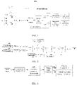
- the entire process of FSK communication is shown in FIG. 1 .
- a value output by the comparator is read at a frequency of 2MHz, and this value can be regarded as 1bit sampling data of 2 MHz.
- the data first passes through a low-pass filter 1 such that the jitter waveform with a higher frequency is filtered out, and then, the period point counting is performed, and values of 256 sampling points are added up.
- the data stream is divided into a left channel and a right channel after passing through the left and right channel generation module, and then the data is respectively smoothed by the low-pass filter 2. Finally, data bit determination is performed on the output of the low-pass filter, so that 0 or 1 is outputted. It is worth noting that the processing subjected by the left and right outputs are completely the same, so the circuit is time-division multiplexing.
- a second-order IIR low-pass filter LPF1 is used for processing.
- This filter includes 6 coefficients, which need to be processed with 8bit fix-point and optimized accordingly.
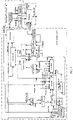
- the output of the period point counting module passes through the left channel and right channel generation module such that the data stream is divided into left and right channels, in which, the left channel signal is a sum of 256 period counts, and the right channel data is obtained by subtracting a variable cons_r from the sum of the 256 period counts under certain conditions, while the calculation process of the above variable is as shown in FIG. 4 .
- the calculation of the period points and the updating process are shown in FIG. 5 . If there is an output from the counter T_counter, the sum of points of the most recent 256 periods is calculated first, and then this outputted value is stored in the period count buffer. After that, a sum of buffer members -- SumTbuff -- is calculated with 256 as a window, and then subsequently processing is performed on SumTbuff.
- the synchronous FIFO is used here to control writing and reading of T_counter. When the starting data is less than 256, T_counter is accumulated and written into the FIFO. When the number of T_counter is greater than 256, the first data in the FIFO is read out and subtracted in SumTbuff before data is written.
- this filter is to smooth the outputted data, and the updating frequency of the input data thereof is Fop or Fmod, while the filter is designed when the maximum value is 205KHz.
- a second-order IIR low-pass filter is used, and the coefficients are processed with 16bit fix-point and optimized accordingly.
- the input signal is first left shifted by 8 bits so as to be expanded into a 23bit signal.
- the LPF2_out signal is output after the SumTbuff passes through the low-pass filter 2, and since the SumTbuff will have a certain fluctuation during the communication, this fluctuation can be regarded as noise at a higher frequency.
- LPF2_out can reflect the change of frequency, and the value of Fop is determined at this time. Then, this value is used to make a difference with the value output by LPF2.
- the differenced signal is subjected to a series of waveform modification processing, thereby eliminating jitter and offset in the sum value in such a manner that only the change value left so as to perform the determination.
- This module is mainly to complete detection of the frequency change, same frequency counting, and elimination of Fop influence on decoding and elimination of jitter.
- the circuit structure for efficiently demodulating an FSK signal in a wireless charging device of the present disclosure since the method described in the period point calculation module, left and right channel data generation module, and the period point processing module mentioned above is used in the demodulation circuit, efficient demodulation can be implemented by a demodulation circuit using only 2M clock processing data. Even if an input signal is poor, demodulation can be performed accurately. The unpacking rate (a number of correct unpackings) is greatly improved. Meanwhile, left and right processing flows are the same, and the circuit is a time-division multiplexing circuit. Thus, the circuit overhead is reduced, FSK signal demodulation is more efficient, and the circuit structure can be widely applied.
Landscapes
- Engineering & Computer Science (AREA)
- Computer Networks & Wireless Communication (AREA)
- Signal Processing (AREA)
- Physics & Mathematics (AREA)
- Spectroscopy & Molecular Physics (AREA)
- Microelectronics & Electronic Packaging (AREA)
- Power Engineering (AREA)
- Digital Transmission Methods That Use Modulated Carrier Waves (AREA)
Claims (10)
- Schaltungsstruktur zur effizienten Demodulation eines Frequency-Shift Keying-, FSK, Signals in einer drahtlosen Ladevorrichtung, wobei die Schaltungsstruktur umfasst:ein Datenabtastmodul, das so konfiguriert ist, dass es Rohdaten von einer Spule empfängt, die Rohdaten glättet und Periodenpunkte in den Daten abtastet;ein Periodenpunkt-Zählmodul, das konfiguriert ist, um eine Summe der Periodenpunkte zu berechnen, wobei das Periodenpunkt-Zählmodul einen Eingangsanschluss hat, der mit einem Ausgangsanschluss des Datenabtastmoduls verbunden ist;ein Datenverteilungsmodul, das so konfiguriert ist, dass es Daten eines linken Kanals und Daten eines rechten Kanals erzeugt und Daten über die Summe der Periodenpunkte in zwei Kanäle aufteilt, um ein Zeitmultiplexen einer Schaltung zu erreichen, und wobei das Datenverteilungsmodul einen Eingangsanschluss hat, der mit einem Ausgangsanschluss des Periodenpunkt-Zählmoduls verbunden ist; undein Periodenpunkt-Verarbeitungsmodul, das so konfiguriert ist, dass es die Daten des linken Kanals und die Daten des rechten Kanals glättet, eine Datenbitbestimmung durchführt und ein demoduliertes FSK-Signal ausgibt, wobei das Periodenpunkt-Verarbeitungsmodul einen Eingangsanschluss hat, der mit einem Ausgangsanschluss des Datenverteilungsmoduls verbunden ist.
- Schaltungsstruktur zur effizienten Demodulation eines FSK-Signals in einem drahtlosen Ladegerät nach Anspruch 1, dadurch gekennzeichnet, dass das Datenabtastmodul umfasst:eine Empfangsspule, die so konfiguriert ist, dass sie Signale von einem Sender empfängt;einen ersten Komparator (Cmp), der so konfiguriert ist, dass er die Rohdaten von der Empfangsspule empfängt und die Rohdaten mit einem Referenzpotential vergleicht, wobei die Rohdaten der Empfangsspule in einen ersten Eingangsanschluss des ersten Komparators (Cmp) eingegeben werden, nachdem sie mit einer Frequenz von 2 MHz abgetastet wurden, und wobei ein zweiter Eingangsanschluss des ersten Komparators (Cmp) mit dem Referenzpotential verbunden ist;einen ersten Tiefpassfilter (LPF1), der so konfiguriert ist, dass er Daten glättet, wobei der erste Tiefpassfilter (LPF1) einen Eingangsanschluss, der mit einem Ausgangsanschluss des ersten Komparators (Cmp) verbunden ist, und einen Ausgangsanschluss zum Übertragen gefilterter Daten an eine Hochfrequenz-Abtasteinheit umfasst; unddie Hochfrequenz-Abtasteinheit so konfiguriert ist, dass sie die Periodenpunkte auf der Grundlage einer ansteigenden Flanke erfasst und abtastet, wobei ein Eingangsanschluss der Hochfrequenz-Abtasteinheit mit dem ersten Tiefpassfilter (LPF1) verbunden ist und ein Ausgangsanschluss der Hochfrequenz-Abtasteinheit mit dem Eingangsanschluss des Periodenpunkt-Zählmoduls verbunden ist.
- Schaltungsstruktur zur effizienten Demodulation eines FSK-Signals in einer drahtlosen Ladevorrichtung nach Anspruch 2, dadurch gekennzeichnet, dass das erste Tiefpassfilter (LPF1) ein IIR-Tiefpassfilter zweiter Ordnung mit einer Grenzfrequenz von 5 kHz und einer Abtastfrequenz von 2 MHz ist.
- Schaltungsstruktur zur effizienten Demodulation eines FSK-Signals in einem drahtlosen Ladegerät nach Anspruch 1, dadurch gekennzeichnet, dass das Periodenpunkt-Zählmodul einen ersten Selektor, einen ersten Addierer und einen zweiten Addierer umfasst, wobei ein erster Eingangsanschluss des ersten Selektors mit einem Ausgangsanschluss des ersten Addierers verbunden ist, und ein zweiter Eingangsanschluss des ersten Selektors mit einem Ausgangsanschluss des zweiten Addierers verbunden ist; der erste Addierer so konfiguriert ist, dass er, wenn eine Anzahl von Malen, die das Datenabtastmodul Daten ausgibt, größer als 256 ist, eine Summe aller Daten berechnet, die von dem Datenabtastmodul ausgegeben werden; der zweite Addierer so konfiguriert ist, dass er, wenn die Anzahl von Malen, die das Datenabtastmodul Daten ausgibt, kleiner oder gleich 256 ist, eine Summe aller Daten berechnet, die von dem Datenabtastmodul ausgegeben werden; und ein Ausgangsanschluss des ersten Selektors selektiv ein Ausgangsergebnis des ersten Addierers oder ein Ausgangsergebnis des zweiten Addierers auf der Grundlage eines Eingangssignals eines Freigabeanschlusses des ersten Selektors ausgibt.
- Schaltungsstruktur zur effizienten Demodulation eines FSK-Signals in einer drahtlosen Ladevorrichtung nach Anspruch 1, dadurch gekennzeichnet, dass das Datenverteilungsmodul ein viertes D-Flip-Flop, ein fünftes D-Flip-Flop, einen fünften Selektor, einen sechsten Selektor, einen achten Komparator und einen fünften Addierer umfasst, wobei ein Eingangsanschluss des vierten D-Flip-Flops mit einem Flag-Signal verbunden ist, ein Ausgangsanschluss des vierten D-Flip-Flops mit einem Freigabeanschluss des fünften Selektors verbunden ist, ein erster Eingangsanschluss des fünften Selektors mit einem Ausgangsanschluss des achten Komparators verbunden ist, ein zweiter Eingangsanschluss des fünften Selektors mit einem Ausgangsanschluss des fünften Addierers verbunden ist, ein Ausgangsanschluss des fünften Selektors mit einem zweiten Eingangsanschluss des sechsten Selektors verbunden ist, ein erster Eingangsanschluss des sechsten Selektors mit einem zweiten Schwellwertsignal verbunden ist, ein Freigabeanschluss des sechsten Selektors mit einem Ausgangsanschluss des fünften D-Flipflops verbunden ist, ein Eingangsanschluss des fünften D-Flipflops mit einem Signal der steigenden Flanke eines Eingangssignals verbunden ist, ein Ausgangsanschluss des sechsten Selektors mit einem zweiten Eingangsanschluss des achten Komparators bzw. einem zweiten Eingangsanschluss des fünften Addierers verbunden ist, ein erster Eingangsanschluss des achten Komparators mit einem ersten Schwellwertsignal verbunden ist und ein erster Eingangsanschluss des fünften Addierers mit Logik 1 verbunden ist.
- Schaltungsstruktur zur effizienten Demodulation eines FSK-Signals in einem drahtlosen Ladegerät nach Anspruch 1, dadurch gekennzeichnet, dass das Periodenpunkt-Verarbeitungsmodul umfasst:einen zweiten Tiefpassfilter, der so konfiguriert ist, dass er die Daten des linken Kanals und die Daten des rechten Kanals glättet, wobei ein Eingangsanschluss des zweiten Tiefpassfilters mit dem Ausgangsanschluss des Datenverteilungsmoduls verbunden ist und ein erster Ausgangsanschluss des zweiten Tiefpassfilters mit einem Rücckopplungsanschluss des Periodenpunkt-Zählmoduls verbunden ist;eine Trägerfrequenz-Fop-Einheit, die so konfiguriert ist, dass sie den Einfluss von Fop auf einen Summenwert der Periodenpunkte eliminiert, wobei die Trägerfrequenz-Fop-Einheit einen Eingangsanschluss umfasst, der mit einem zweiten Ausgangsanschluss des zweiten Tiefpassfilters verbunden ist;eine Frequenz-Jitter-Eliminierungseinheit, die so konfiguriert ist, dass sie Jitter und Offset in dem Summenwert der Periodenpunkte eliminiert, so dass nur ein Periodenänderungswert in den Daten übrig bleibt, wobei der Ausgangsanschluss der Trägerfrequenz-Fop-Einheit mit einem Eingangsanschluss der Frequenz-Jitter-Eliminierungseinheit verbunden ist; undeine Wellenformmodifizierungseinheit, die so konfiguriert ist, dass sie eine ausgegebene Wellenform innerhalb eines bestimmten numerischen Bereichs modifiziert, wobei der Ausgangsanschluss der Trägerfrequenz-Fop-Einheit mit einem Eingangsanschluss der Wellenformmodifizierungseinheit verbunden ist, ein Ausgangsanschluss der Frequenz-Jitter-Eliminierungseinheit mit einem Steueranschluss der Wellenformmodifizierungseinheit verbunden ist und ein Ausgangsanschluss der Wellenformmodifizierungseinheit ein Ausgangsanschluss der Schaltungsstruktur ist.
- Schaltungsstruktur zur effizienten Demodulation eines FSK-Signals in einer drahtlosen Ladevorrichtung nach Anspruch 6, dadurch gekennzeichnet, dass das zweite Tiefpassfilter ein IIR-Tiefpassfilter zweiter Ordnung mit einer Grenzfrequenz von 5 kHz und einer Abtastfrequenz von 210 kHz ist.
- Schaltungsstruktur zur effizienten Demodulation eines FSK-Signals in einem drahtlosen Ladegerät nach Anspruch 6, dadurch gekennzeichnet, dass die Trägerfrequenz-Fop-Einheit einen ersten Subtrahierer, einen zweiten Subtrahierer, ein erstes D-Flipflop, ein zweites D-Flipflop, ein drittes D-Flipflop, einen ersten Komparator, einen zweiten Komparator, einen fünften Komparator, einen sechsten Komparator, einen siebten Komparator, einen dritten Addierer, einen vierten Addierer, einen zweiten Selektor, einen dritten Selektor, ein erstes UND-Gatter, ein zweites UND-Gatter, ein Schieberegister und eine zweite Untereinheit zur Gewinnung des Absolutwerts aufweist, wobei die Ausgangsanschlüsse des zweiten Tiefpassfilters mit einem ersten Eingangsanschluss des ersten Subtrahierers bzw. einem Eingangsanschluss des ersten D-Flipflops verbunden sind, ein Ausgangsanschluss des ersten D-Flipflops mit einem zweiten Eingangsanschluss des ersten Subtrahierers verbunden ist, ein Ausgangsanschluss des ersten Subtrahierers mit einem ersten Eingangsanschluss des ersten Komparators verbunden ist, ein zweiter Eingangsanschluss des ersten Komparators mit einem logischen Signal 0 verbunden ist, ein Ausgangsanschluss des ersten Komparators mit einem Freigabeanschluss des dritten Addierers verbunden ist, ein Ausgangsanschluss des dritten Addierers mit einem ersten Eingangsanschluss des zweiten Selektors verbunden ist, ein zweiter Eingangsanschluss des zweiten Selektors mit dem logischen Signal 0 verbunden ist, ein Ausgangsanschluss des zweiten Selektors jeweils mit einem Eingangsanschluss des dritten Addierers und einem ersten Eingangsanschluss des zweiten Komparators verbunden ist, ein erster Freigabesignalanschluss des zweiten Selektors mit einem Ausgangsanschluss des ersten UND-Gatters verbunden ist, ein zweiter Freigabeanschluss des zweiten Selektors mit einem ansteigenden Flankensignal eines Eingangssignals verbunden ist, ein dritter Freigabeanschluss des zweiten Selektors mit einem Freigabesignal der Schaltungsstruktur verbunden ist, ein vierter Freigabeanschluss des zweiten Selektors mit einem Rücksetzsignal der Schaltungsstruktur verbunden ist, und ein fünfter Freigabeanschluss des zweiten Selektors mit einem Taktsignal der Schaltungsstruktur verbunden ist; ein zweiter Eingangsanschluss des zweiten Komparators ist mit einem fünften Schwellwertsignal verbunden, ein Ausgangsanschluss des zweiten Komparators ist mit einem ersten Eingangsanschluss des ersten UND-Gatters verbunden, ein zweiter Eingangsanschluss des ersten UND-Gatters ist mit dem Signal der ansteigenden Flanke des Eingangssignals verbunden, der Ausgangsanschluss des ersten UND-Gatters ist auch mit einem ersten Freigabeanschluss des zweiten D-Flipflops verbunden, ein Eingangsanschluss des zweiten D-Flipflops ist mit den Ausgangsanschlüssen des zweiten Tiefpassfilters verbunden, ein Ausgangsanschluss des zweiten D-Flipflops ist mit einem zweiten Eingangsanschluss des zweiten Subtrahierers verbunden, ein erster Eingangsanschluss des zweiten Subtrahierers ist mit dem Ausgangsanschluss des zweiten Tiefpassfilters verbunden, ein Taktanschluss des zweiten Subtrahierers ist mit dem Signal der ansteigenden Flanke des Eingangssignals verbunden, ein Ausgangsanschluss des zweiten Subtrahierers ist jeweils mit dem Eingangsanschluss der Frequenz-Jitter-Eliminierungseinheit, dem Eingangsanschluss der Wellenformmodifikationseinheit und einem Eingangsanschluss der zweiten Untereinheit zur Gewinnung des absoluten Werts verbunden, ein Ausgangsanschluss der Untereinheit zur Gewinnung des zweiten Absolutwerts ist mit einem ersten Eingangsanschluss des fünften Komparators verbunden, ein zweiter Eingangsanschluss des fünften Komparators ist mit einem dritten Schwellwertsignal verbunden, ein Ausgangsanschluss des fünften Komparators ist mit einem ersten Eingangsanschluss des zweiten UND-Gatters verbunden, und ein Ausgangsanschluss des zweiten UND-Gatters ist mit einem zweiten Freigabeanschluss des zweiten D-Flipflops verbunden; der Ausgangsanschluss des zweiten Tiefpassfilters ist auch mit dem Schieberegister verbunden, ein Taktanschluss des Schieberegisters ist mit dem Signal der ansteigenden Flanke des Eingangssignals verbunden, ein Ausgangsanschluss des Schieberegisters ist mit einem ersten Eingangsanschluss des sechsten Komparators und einem Eingangsanschluss des dritten D-Flipflops verbunden, ein Ausgangsanschluss des dritten D-Flipflops ist mit einem zweiten Eingangsanschluss des sechsten Komparators verbunden, ein Ausgangsanschluss des sechsten Komparators mit einem Freigabeanschluss des vierten Addierers verbunden ist, ein Taktanschluss des vierten Addierers mit dem Signal der steigenden Flanke des Eingangssignals verbunden ist, ein Ausgangsanschluss des vierten Addierers ist mit einem ersten Eingangsanschluss des dritten Selektors verbunden, ein Ausgangsanschluss des dritten Selektors ist mit einem Eingangsanschluss des vierten Addierers und einem ersten Eingangsanschluss des siebten Komparators verbunden, ein zweiter Eingangsanschluss des dritten Selektors ist mit der logischen 0 verbunden, ein zweiter Eingangsanschluss des siebten Komparators ist mit einem sechsten Schwellwertsignal verbunden, ein Ausgangsanschluss des siebten Komparators ist mit einem zweiten Eingangsanschluss des zweiten UND-Gatters verbunden, ein dritter Eingangsanschluss des zweiten UND-Gatters ist mit dem Signal der ansteigenden Flanke des Eingangssignals verbunden ist, der Ausgangsanschluss des zweiten UND-Gatters ist auch mit einem ersten Freigabeanschluss des dritten Selektors verbunden, ein zweiter Freigabeanschluss des dritten Selektors ist mit dem Freigabesignal der Schaltungsstruktur verbunden, ein dritter Freigabeanschluss des dritten Selektors ist mit dem Rücksetzsignal der Schaltungsstruktur verbunden, und ein vierter Freigabeanschluss des dritten Selektors ist mit dem Ausgangsanschluss des ersten UND-Gatters verbunden; ein fünfter Freigabeanschluss des dritten Selektors ist mit dem Signal der ansteigenden Flanke des Eingangssignals verbunden, und ein sechster Freigabeanschluss des dritten Selektors ist mit dem Taktsignal der Schaltungsstruktur verbunden.
- Schaltungsstruktur zur effizienten Demodulation eines FSK-Signals in einer drahtlosen Ladevorrichtung nach Anspruch 8, dadurch gekennzeichnet, dass die Frequenz-Jitter-Eliminierungseinheit eine erste Untereinheit zur Gewinnung eines Absolutwerts, einen dritten Komparator und einen vierten Komparator umfasst, ein Ausgangsanschluss des zweiten Subtrahierers mit einem Eingangsanschluss der ersten Untereinheit zur Gewinnung eines Absolutwerts verbunden ist, ein Ausgangsanschluss der ersten Untereinheit zur Gewinnung des absoluten Werts mit einem ersten Eingangsanschluss des dritten Komparators bzw. einem ersten Eingangsanschluss des vierten Komparators verbunden ist, ein zweiter Eingangsanschluss des dritten Komparators mit einem vierten Schwellwertsignal verbunden ist, ein zweiter Eingangsanschluss des vierten Komparators mit dem dritten Schwellwertsignal verbunden ist, und ein Ausgangsanschluss des dritten Komparators und ein Ausgangsanschluss des vierten Komparators beide mit dem Steueranschluss der Wellenformmodifikationseinheit verbunden sind.
- Schaltungsstruktur zur effizienten Demodulation eines FSK-Signals in einer drahtlosen Ladevorrichtung nach Anspruch 9, dadurch gekennzeichnet, dass die Wellenformmodifikationseinheit der vierte Selektor ist, ein erster Freigabesignalanschluss eines vierten Selektors mit dem Ausgangsanschluss des dritten Komparators verbunden ist, ein zweiter Freigabesignalanschluss des vierten Selektors mit einem Ausgangsanschluss des vierten Komparators verbunden ist, ein erster Eingangsanschluss des vierten Selektors mit dem Ausgangsanschluss des zweiten Subtrahierers verbunden ist, ein zweiter Eingangsanschluss des vierten Selektors mit Logik 1 verbunden ist, ein dritter Eingangsanschluss des vierten Selektors mit einem zweiten Schwellwertsignal verbunden ist, und ein Ausgangsanschluss des vierten Selektors ein Ausgangsanschluss der Schaltungsstruktur ist.
Applications Claiming Priority (2)
| Application Number | Priority Date | Filing Date | Title |
|---|---|---|---|
| CN201610958222.3A CN106532969B (zh) | 2016-11-03 | 2016-11-03 | 无线充电设备中实现fsk信号高效解调的电路结构 |
| PCT/CN2017/095078 WO2018082357A1 (zh) | 2016-11-03 | 2017-07-29 | 无线充电设备中实现fsk信号高效解调的电路结构 |
Publications (3)
| Publication Number | Publication Date |
|---|---|
| EP3512170A1 EP3512170A1 (de) | 2019-07-17 |
| EP3512170A4 EP3512170A4 (de) | 2020-04-29 |
| EP3512170B1 true EP3512170B1 (de) | 2022-04-06 |
Family
ID=58326026
Family Applications (1)
| Application Number | Title | Priority Date | Filing Date |
|---|---|---|---|
| EP17867412.3A Active EP3512170B1 (de) | 2016-11-03 | 2017-07-29 | Schaltstruktur zur effizienten demodulation von fsk-signalen bei einer drahtlosen ladevorrichtung |
Country Status (4)
| Country | Link |
|---|---|
| US (1) | US10700903B2 (de) |
| EP (1) | EP3512170B1 (de) |
| CN (1) | CN106532969B (de) |
| WO (1) | WO2018082357A1 (de) |
Families Citing this family (9)
| Publication number | Priority date | Publication date | Assignee | Title |
|---|---|---|---|---|
| CN106532969B (zh) * | 2016-11-03 | 2018-06-12 | 无锡华润矽科微电子有限公司 | 无线充电设备中实现fsk信号高效解调的电路结构 |
| CN109698803B (zh) * | 2017-10-20 | 2023-09-08 | 华润微集成电路(无锡)有限公司 | 无线充电设备中实现fsk信号高效解调的电路结构 |
| CN110896311B (zh) * | 2018-08-22 | 2021-05-18 | 华润微集成电路(无锡)有限公司 | 针对pma标准的无线充电设备调频信号的解码电路 |
| US11139664B2 (en) * | 2018-09-11 | 2021-10-05 | Texas Instruments Incorporated | Battery protector hibernate input separate from VDD, low power output |
| CN110865217B (zh) * | 2019-12-13 | 2024-10-11 | 珠海市运泰利自动化设备有限公司 | 一种用于充电器主板信号测试的2fsk解调电路及方法 |
| CN113555978B (zh) * | 2020-04-23 | 2022-10-21 | 深圳市万普拉斯科技有限公司 | 无线充电放偏检测方法、装置、电子设备和存储介质 |
| CN113395228B (zh) * | 2021-06-10 | 2022-08-23 | 深圳清华大学研究院 | 一种针对2fsk信号的解调电路 |
| CN114675757B (zh) * | 2022-03-25 | 2024-12-27 | 合肥智芯半导体有限公司 | 触摸感应输入模块及其基准点和阈值更新装置 |
| CN115189447B (zh) * | 2022-08-02 | 2023-05-16 | 深圳市诚芯微科技股份有限公司 | 一种采用数字控制方式的充电电路及充电控制方法 |
Family Cites Families (14)
| Publication number | Priority date | Publication date | Assignee | Title |
|---|---|---|---|---|
| DE2912854A1 (de) * | 1979-03-30 | 1980-10-09 | Itt Ind Gmbh Deutsche | Demodulationsverfahren fuer binaere frequenzmodulierte signale |
| JPH0626349B2 (ja) * | 1989-08-30 | 1994-04-06 | 慶太郎 関根 | Fsk信号復調器 |
| CN101309069B (zh) * | 2007-05-16 | 2010-06-23 | 华为技术有限公司 | 解调电路、数字微波系统和解调方法 |
| JP5100797B2 (ja) * | 2010-08-09 | 2012-12-19 | 株式会社九州テン | デジタル無線信号の復調回路およびそれを用いた無線受信装置 |
| JP2013546255A (ja) * | 2010-11-03 | 2013-12-26 | エックスペッド ホールディングス ピーティワイ リミテッド | 無線デバイス検出ならびに通信装置およびシステム |
| CN102325109B (zh) * | 2011-06-13 | 2013-09-04 | 浙江大学 | 一种快速fsk解调方法及全数字低功耗实现装置 |
| AU2013239344A1 (en) * | 2012-03-28 | 2014-10-09 | Xped Holdings Pty Ltd | Method and apparatus for forming associations and communicating between devices |
| JP6284315B2 (ja) * | 2013-08-13 | 2018-02-28 | ローム株式会社 | 非接触給電システム、受信機器、およびアナログ回路 |
| JP6198630B2 (ja) * | 2014-02-25 | 2017-09-20 | パナソニック株式会社 | 受信装置及び復調方法 |
| CN106300576B (zh) * | 2015-05-11 | 2021-04-20 | 恩智浦美国有限公司 | 用于无线充电系统的双向通信解调方法 |
| CN105516040B (zh) * | 2015-11-30 | 2019-01-08 | 无锡华润矽科微电子有限公司 | 无线充电设备中fsk信号的低消耗解调方法 |
| CN106534015B (zh) * | 2016-11-03 | 2018-02-09 | 无锡华润矽科微电子有限公司 | 针对pma标准的无线充电设备调频信号的解调方法 |
| CN106532969B (zh) * | 2016-11-03 | 2018-06-12 | 无锡华润矽科微电子有限公司 | 无线充电设备中实现fsk信号高效解调的电路结构 |
| US10840746B2 (en) * | 2018-06-20 | 2020-11-17 | Apple Inc. | Methods and apparatus for performing demodulation using maximum likelihood sequence matching in a wireless charging device |
-
2016
- 2016-11-03 CN CN201610958222.3A patent/CN106532969B/zh active Active
-
2017
- 2017-07-29 WO PCT/CN2017/095078 patent/WO2018082357A1/zh not_active Ceased
- 2017-07-29 US US16/337,526 patent/US10700903B2/en active Active
- 2017-07-29 EP EP17867412.3A patent/EP3512170B1/de active Active
Also Published As
| Publication number | Publication date |
|---|---|
| EP3512170A1 (de) | 2019-07-17 |
| US10700903B2 (en) | 2020-06-30 |
| CN106532969B (zh) | 2018-06-12 |
| WO2018082357A1 (zh) | 2018-05-11 |
| US20190253289A1 (en) | 2019-08-15 |
| EP3512170A4 (de) | 2020-04-29 |
| CN106532969A (zh) | 2017-03-22 |
Similar Documents
| Publication | Publication Date | Title |
|---|---|---|
| EP3512170B1 (de) | Schaltstruktur zur effizienten demodulation von fsk-signalen bei einer drahtlosen ladevorrichtung | |
| US9203665B1 (en) | Resource optimization by implementing multiple instances of a soft modem with a single microcontroller | |
| EP3264699B1 (de) | Rfid-empfänger und verfahren zur extraktion von in einem funksignal codierten datenbits | |
| US9106488B1 (en) | Energy efficient highway addressable remote transducer soft modem | |
| US9893771B2 (en) | Wireless charger using frequency aliasing FSK demodulation | |
| CN105516040B (zh) | 无线充电设备中fsk信号的低消耗解调方法 | |
| CN203574663U (zh) | 一种自动波特率检测模块 | |
| CN107483078A (zh) | 一种船舶vdes系统asm体制接收频偏估计实现方法 | |
| CN104393885A (zh) | 一种用于无人机地空宽带通信系统的接收终端及其方法 | |
| CN103812505B (zh) | 位同步锁定检测器 | |
| CN110635892A (zh) | 基于同步422标准的数据采样系统 | |
| CN105376041B (zh) | 异步串行数据采集装置以及异步串行数据采集方法 | |
| CN114490488B (zh) | 一种低功耗uart串口系统 | |
| CN104363193B (zh) | 一种用于无人机地空宽带通信系统的接收终端方法 | |
| CN109698803B (zh) | 无线充电设备中实现fsk信号高效解调的电路结构 | |
| CN110896311B (zh) | 针对pma标准的无线充电设备调频信号的解码电路 | |
| EP4187859B1 (de) | Vorrichtung und verfahren zur decodierung von daten aus drahtlosen signalen | |
| KR20110096403A (ko) | 제로크로싱복조를 이용한 fsk수신기 및 이의 제어방법 | |
| CN110071732B (zh) | 一种低功耗无线接收方法及其接收系统 | |
| CN113542181B (zh) | 频偏估计方法、装置、设备及计算机可读存储介质 | |
| CN113395228B (zh) | 一种针对2fsk信号的解调电路 | |
| CN110337785B (zh) | 用于调制解调器的杂散消除系统 | |
| CN107562662B (zh) | 一种将spi信号转换为ssi信号的转换方法及电路 | |
| CN103338173A (zh) | 一种恢复码元的方法、装置 | |
| CN110750479A (zh) | 基于同步422标准的数据采样方法 |
Legal Events
| Date | Code | Title | Description |
|---|---|---|---|
| STAA | Information on the status of an ep patent application or granted ep patent |
Free format text: STATUS: THE INTERNATIONAL PUBLICATION HAS BEEN MADE |
|
| PUAI | Public reference made under article 153(3) epc to a published international application that has entered the european phase |
Free format text: ORIGINAL CODE: 0009012 |
|
| STAA | Information on the status of an ep patent application or granted ep patent |
Free format text: STATUS: REQUEST FOR EXAMINATION WAS MADE |
|
| 17P | Request for examination filed |
Effective date: 20190328 |
|
| AK | Designated contracting states |
Kind code of ref document: A1 Designated state(s): AL AT BE BG CH CY CZ DE DK EE ES FI FR GB GR HR HU IE IS IT LI LT LU LV MC MK MT NL NO PL PT RO RS SE SI SK SM TR |
|
| AX | Request for extension of the european patent |
Extension state: BA ME |
|
| DAV | Request for validation of the european patent (deleted) | ||
| DAX | Request for extension of the european patent (deleted) | ||
| A4 | Supplementary search report drawn up and despatched |
Effective date: 20200401 |
|
| RIC1 | Information provided on ipc code assigned before grant |
Ipc: H04B 5/00 20060101ALI20200326BHEP Ipc: H04L 27/148 20060101AFI20200326BHEP |
|
| RAP3 | Party data changed (applicant data changed or rights of an application transferred) |
Owner name: CRM ICBG (WUXI) CO., LTD. |
|
| GRAP | Despatch of communication of intention to grant a patent |
Free format text: ORIGINAL CODE: EPIDOSNIGR1 |
|
| STAA | Information on the status of an ep patent application or granted ep patent |
Free format text: STATUS: GRANT OF PATENT IS INTENDED |
|
| INTG | Intention to grant announced |
Effective date: 20211029 |
|
| GRAS | Grant fee paid |
Free format text: ORIGINAL CODE: EPIDOSNIGR3 |
|
| GRAA | (expected) grant |
Free format text: ORIGINAL CODE: 0009210 |
|
| STAA | Information on the status of an ep patent application or granted ep patent |
Free format text: STATUS: THE PATENT HAS BEEN GRANTED |
|
| AK | Designated contracting states |
Kind code of ref document: B1 Designated state(s): AL AT BE BG CH CY CZ DE DK EE ES FI FR GB GR HR HU IE IS IT LI LT LU LV MC MK MT NL NO PL PT RO RS SE SI SK SM TR |
|
| REG | Reference to a national code |
Ref country code: GB Ref legal event code: FG4D |
|
| REG | Reference to a national code |
Ref country code: CH Ref legal event code: EP |
|
| REG | Reference to a national code |
Ref country code: AT Ref legal event code: REF Ref document number: 1482432 Country of ref document: AT Kind code of ref document: T Effective date: 20220415 |
|
| REG | Reference to a national code |
Ref country code: IE Ref legal event code: FG4D |
|
| REG | Reference to a national code |
Ref country code: DE Ref legal event code: R096 Ref document number: 602017055732 Country of ref document: DE |
|
| REG | Reference to a national code |
Ref country code: NL Ref legal event code: FP |
|
| REG | Reference to a national code |
Ref country code: LT Ref legal event code: MG9D |
|
| REG | Reference to a national code |
Ref country code: AT Ref legal event code: MK05 Ref document number: 1482432 Country of ref document: AT Kind code of ref document: T Effective date: 20220406 |
|
| PG25 | Lapsed in a contracting state [announced via postgrant information from national office to epo] |
Ref country code: SE Free format text: LAPSE BECAUSE OF FAILURE TO SUBMIT A TRANSLATION OF THE DESCRIPTION OR TO PAY THE FEE WITHIN THE PRESCRIBED TIME-LIMIT Effective date: 20220406 Ref country code: PT Free format text: LAPSE BECAUSE OF FAILURE TO SUBMIT A TRANSLATION OF THE DESCRIPTION OR TO PAY THE FEE WITHIN THE PRESCRIBED TIME-LIMIT Effective date: 20220808 Ref country code: NO Free format text: LAPSE BECAUSE OF FAILURE TO SUBMIT A TRANSLATION OF THE DESCRIPTION OR TO PAY THE FEE WITHIN THE PRESCRIBED TIME-LIMIT Effective date: 20220706 Ref country code: LT Free format text: LAPSE BECAUSE OF FAILURE TO SUBMIT A TRANSLATION OF THE DESCRIPTION OR TO PAY THE FEE WITHIN THE PRESCRIBED TIME-LIMIT Effective date: 20220406 Ref country code: HR Free format text: LAPSE BECAUSE OF FAILURE TO SUBMIT A TRANSLATION OF THE DESCRIPTION OR TO PAY THE FEE WITHIN THE PRESCRIBED TIME-LIMIT Effective date: 20220406 Ref country code: GR Free format text: LAPSE BECAUSE OF FAILURE TO SUBMIT A TRANSLATION OF THE DESCRIPTION OR TO PAY THE FEE WITHIN THE PRESCRIBED TIME-LIMIT Effective date: 20220707 Ref country code: FI Free format text: LAPSE BECAUSE OF FAILURE TO SUBMIT A TRANSLATION OF THE DESCRIPTION OR TO PAY THE FEE WITHIN THE PRESCRIBED TIME-LIMIT Effective date: 20220406 Ref country code: ES Free format text: LAPSE BECAUSE OF FAILURE TO SUBMIT A TRANSLATION OF THE DESCRIPTION OR TO PAY THE FEE WITHIN THE PRESCRIBED TIME-LIMIT Effective date: 20220406 Ref country code: BG Free format text: LAPSE BECAUSE OF FAILURE TO SUBMIT A TRANSLATION OF THE DESCRIPTION OR TO PAY THE FEE WITHIN THE PRESCRIBED TIME-LIMIT Effective date: 20220706 Ref country code: AT Free format text: LAPSE BECAUSE OF FAILURE TO SUBMIT A TRANSLATION OF THE DESCRIPTION OR TO PAY THE FEE WITHIN THE PRESCRIBED TIME-LIMIT Effective date: 20220406 |
|
| PG25 | Lapsed in a contracting state [announced via postgrant information from national office to epo] |
Ref country code: RS Free format text: LAPSE BECAUSE OF FAILURE TO SUBMIT A TRANSLATION OF THE DESCRIPTION OR TO PAY THE FEE WITHIN THE PRESCRIBED TIME-LIMIT Effective date: 20220406 Ref country code: PL Free format text: LAPSE BECAUSE OF FAILURE TO SUBMIT A TRANSLATION OF THE DESCRIPTION OR TO PAY THE FEE WITHIN THE PRESCRIBED TIME-LIMIT Effective date: 20220406 Ref country code: LV Free format text: LAPSE BECAUSE OF FAILURE TO SUBMIT A TRANSLATION OF THE DESCRIPTION OR TO PAY THE FEE WITHIN THE PRESCRIBED TIME-LIMIT Effective date: 20220406 Ref country code: IS Free format text: LAPSE BECAUSE OF FAILURE TO SUBMIT A TRANSLATION OF THE DESCRIPTION OR TO PAY THE FEE WITHIN THE PRESCRIBED TIME-LIMIT Effective date: 20220806 |
|
| REG | Reference to a national code |
Ref country code: DE Ref legal event code: R097 Ref document number: 602017055732 Country of ref document: DE |
|
| PG25 | Lapsed in a contracting state [announced via postgrant information from national office to epo] |
Ref country code: SM Free format text: LAPSE BECAUSE OF FAILURE TO SUBMIT A TRANSLATION OF THE DESCRIPTION OR TO PAY THE FEE WITHIN THE PRESCRIBED TIME-LIMIT Effective date: 20220406 Ref country code: SK Free format text: LAPSE BECAUSE OF FAILURE TO SUBMIT A TRANSLATION OF THE DESCRIPTION OR TO PAY THE FEE WITHIN THE PRESCRIBED TIME-LIMIT Effective date: 20220406 Ref country code: RO Free format text: LAPSE BECAUSE OF FAILURE TO SUBMIT A TRANSLATION OF THE DESCRIPTION OR TO PAY THE FEE WITHIN THE PRESCRIBED TIME-LIMIT Effective date: 20220406 Ref country code: EE Free format text: LAPSE BECAUSE OF FAILURE TO SUBMIT A TRANSLATION OF THE DESCRIPTION OR TO PAY THE FEE WITHIN THE PRESCRIBED TIME-LIMIT Effective date: 20220406 Ref country code: DK Free format text: LAPSE BECAUSE OF FAILURE TO SUBMIT A TRANSLATION OF THE DESCRIPTION OR TO PAY THE FEE WITHIN THE PRESCRIBED TIME-LIMIT Effective date: 20220406 Ref country code: CZ Free format text: LAPSE BECAUSE OF FAILURE TO SUBMIT A TRANSLATION OF THE DESCRIPTION OR TO PAY THE FEE WITHIN THE PRESCRIBED TIME-LIMIT Effective date: 20220406 |
|
| PLBE | No opposition filed within time limit |
Free format text: ORIGINAL CODE: 0009261 |
|
| STAA | Information on the status of an ep patent application or granted ep patent |
Free format text: STATUS: NO OPPOSITION FILED WITHIN TIME LIMIT |
|
| PG25 | Lapsed in a contracting state [announced via postgrant information from national office to epo] |
Ref country code: MC Free format text: LAPSE BECAUSE OF FAILURE TO SUBMIT A TRANSLATION OF THE DESCRIPTION OR TO PAY THE FEE WITHIN THE PRESCRIBED TIME-LIMIT Effective date: 20220406 |
|
| REG | Reference to a national code |
Ref country code: CH Ref legal event code: PL |
|
| 26N | No opposition filed |
Effective date: 20230110 |
|
| REG | Reference to a national code |
Ref country code: BE Ref legal event code: MM Effective date: 20220731 |
|
| PG25 | Lapsed in a contracting state [announced via postgrant information from national office to epo] |
Ref country code: AL Free format text: LAPSE BECAUSE OF FAILURE TO SUBMIT A TRANSLATION OF THE DESCRIPTION OR TO PAY THE FEE WITHIN THE PRESCRIBED TIME-LIMIT Effective date: 20220406 |
|
| PG25 | Lapsed in a contracting state [announced via postgrant information from national office to epo] |
Ref country code: LU Free format text: LAPSE BECAUSE OF NON-PAYMENT OF DUE FEES Effective date: 20220729 Ref country code: LI Free format text: LAPSE BECAUSE OF NON-PAYMENT OF DUE FEES Effective date: 20220731 Ref country code: CH Free format text: LAPSE BECAUSE OF NON-PAYMENT OF DUE FEES Effective date: 20220731 |
|
| PG25 | Lapsed in a contracting state [announced via postgrant information from national office to epo] |
Ref country code: SI Free format text: LAPSE BECAUSE OF FAILURE TO SUBMIT A TRANSLATION OF THE DESCRIPTION OR TO PAY THE FEE WITHIN THE PRESCRIBED TIME-LIMIT Effective date: 20220406 Ref country code: BE Free format text: LAPSE BECAUSE OF NON-PAYMENT OF DUE FEES Effective date: 20220731 |
|
| PG25 | Lapsed in a contracting state [announced via postgrant information from national office to epo] |
Ref country code: IE Free format text: LAPSE BECAUSE OF NON-PAYMENT OF DUE FEES Effective date: 20220729 |
|
| PG25 | Lapsed in a contracting state [announced via postgrant information from national office to epo] |
Ref country code: IT Free format text: LAPSE BECAUSE OF FAILURE TO SUBMIT A TRANSLATION OF THE DESCRIPTION OR TO PAY THE FEE WITHIN THE PRESCRIBED TIME-LIMIT Effective date: 20220406 |
|
| PG25 | Lapsed in a contracting state [announced via postgrant information from national office to epo] |
Ref country code: HU Free format text: LAPSE BECAUSE OF FAILURE TO SUBMIT A TRANSLATION OF THE DESCRIPTION OR TO PAY THE FEE WITHIN THE PRESCRIBED TIME-LIMIT; INVALID AB INITIO Effective date: 20170729 |
|
| PG25 | Lapsed in a contracting state [announced via postgrant information from national office to epo] |
Ref country code: MK Free format text: LAPSE BECAUSE OF FAILURE TO SUBMIT A TRANSLATION OF THE DESCRIPTION OR TO PAY THE FEE WITHIN THE PRESCRIBED TIME-LIMIT Effective date: 20220406 Ref country code: CY Free format text: LAPSE BECAUSE OF FAILURE TO SUBMIT A TRANSLATION OF THE DESCRIPTION OR TO PAY THE FEE WITHIN THE PRESCRIBED TIME-LIMIT Effective date: 20220406 |
|
| PG25 | Lapsed in a contracting state [announced via postgrant information from national office to epo] |
Ref country code: MT Free format text: LAPSE BECAUSE OF FAILURE TO SUBMIT A TRANSLATION OF THE DESCRIPTION OR TO PAY THE FEE WITHIN THE PRESCRIBED TIME-LIMIT Effective date: 20220406 |
|
| PG25 | Lapsed in a contracting state [announced via postgrant information from national office to epo] |
Ref country code: BG Free format text: LAPSE BECAUSE OF FAILURE TO SUBMIT A TRANSLATION OF THE DESCRIPTION OR TO PAY THE FEE WITHIN THE PRESCRIBED TIME-LIMIT Effective date: 20220406 |
|
| PG25 | Lapsed in a contracting state [announced via postgrant information from national office to epo] |
Ref country code: BG Free format text: LAPSE BECAUSE OF FAILURE TO SUBMIT A TRANSLATION OF THE DESCRIPTION OR TO PAY THE FEE WITHIN THE PRESCRIBED TIME-LIMIT Effective date: 20220406 |
|
| PGFP | Annual fee paid to national office [announced via postgrant information from national office to epo] |
Ref country code: GB Payment date: 20250625 Year of fee payment: 9 |
|
| PGFP | Annual fee paid to national office [announced via postgrant information from national office to epo] |
Ref country code: NL Payment date: 20250626 Year of fee payment: 9 |
|
| PGFP | Annual fee paid to national office [announced via postgrant information from national office to epo] |
Ref country code: FR Payment date: 20250626 Year of fee payment: 9 |
|
| PGFP | Annual fee paid to national office [announced via postgrant information from national office to epo] |
Ref country code: DE Payment date: 20250722 Year of fee payment: 9 |
|
| PG25 | Lapsed in a contracting state [announced via postgrant information from national office to epo] |
Ref country code: TR Free format text: LAPSE BECAUSE OF FAILURE TO SUBMIT A TRANSLATION OF THE DESCRIPTION OR TO PAY THE FEE WITHIN THE PRESCRIBED TIME-LIMIT Effective date: 20220406 |