EP3506506A1 - Protection circuit and method for controllable switch - Google Patents
Protection circuit and method for controllable switch Download PDFInfo
- Publication number
- EP3506506A1 EP3506506A1 EP18213755.4A EP18213755A EP3506506A1 EP 3506506 A1 EP3506506 A1 EP 3506506A1 EP 18213755 A EP18213755 A EP 18213755A EP 3506506 A1 EP3506506 A1 EP 3506506A1
- Authority
- EP
- European Patent Office
- Prior art keywords
- terminal
- controllable switch
- coupled
- voltage
- control terminal
- Prior art date
- Legal status (The legal status is an assumption and is not a legal conclusion. Google has not performed a legal analysis and makes no representation as to the accuracy of the status listed.)
- Withdrawn
Links
- 238000000034 method Methods 0.000 title claims abstract description 10
- 238000013016 damping Methods 0.000 claims abstract description 29
- 230000010355 oscillation Effects 0.000 claims abstract description 10
- 239000003990 capacitor Substances 0.000 claims description 17
- 230000000630 rising effect Effects 0.000 claims description 6
- 230000002146 bilateral effect Effects 0.000 claims description 5
- 230000005669 field effect Effects 0.000 claims description 3
- 239000004065 semiconductor Substances 0.000 claims description 3
- 230000001052 transient effect Effects 0.000 claims description 3
- 230000015556 catabolic process Effects 0.000 description 8
- 230000007423 decrease Effects 0.000 description 2
- 238000013461 design Methods 0.000 description 2
- 238000007599 discharging Methods 0.000 description 2
- 238000004519 manufacturing process Methods 0.000 description 2
- 230000000694 effects Effects 0.000 description 1
Images



Classifications
-
- H—ELECTRICITY
- H03—ELECTRONIC CIRCUITRY
- H03K—PULSE TECHNIQUE
- H03K17/00—Electronic switching or gating, i.e. not by contact-making and –breaking
- H03K17/08—Modifications for protecting switching circuit against overcurrent or overvoltage
- H03K17/081—Modifications for protecting switching circuit against overcurrent or overvoltage without feedback from the output circuit to the control circuit
- H03K17/0812—Modifications for protecting switching circuit against overcurrent or overvoltage without feedback from the output circuit to the control circuit by measures taken in the control circuit
- H03K17/08122—Modifications for protecting switching circuit against overcurrent or overvoltage without feedback from the output circuit to the control circuit by measures taken in the control circuit in field-effect transistor switches
-
- H—ELECTRICITY
- H03—ELECTRONIC CIRCUITRY
- H03K—PULSE TECHNIQUE
- H03K17/00—Electronic switching or gating, i.e. not by contact-making and –breaking
- H03K17/08—Modifications for protecting switching circuit against overcurrent or overvoltage
- H03K17/082—Modifications for protecting switching circuit against overcurrent or overvoltage by feedback from the output to the control circuit
- H03K17/0822—Modifications for protecting switching circuit against overcurrent or overvoltage by feedback from the output to the control circuit in field-effect transistor switches
-
- H—ELECTRICITY
- H02—GENERATION; CONVERSION OR DISTRIBUTION OF ELECTRIC POWER
- H02H—EMERGENCY PROTECTIVE CIRCUIT ARRANGEMENTS
- H02H7/00—Emergency protective circuit arrangements specially adapted for specific types of electric machines or apparatus or for sectionalised protection of cable or line systems, and effecting automatic switching in the event of an undesired change from normal working conditions
- H02H7/20—Emergency protective circuit arrangements specially adapted for specific types of electric machines or apparatus or for sectionalised protection of cable or line systems, and effecting automatic switching in the event of an undesired change from normal working conditions for electronic equipment
- H02H7/205—Emergency protective circuit arrangements specially adapted for specific types of electric machines or apparatus or for sectionalised protection of cable or line systems, and effecting automatic switching in the event of an undesired change from normal working conditions for electronic equipment for controlled semi-conductors which are not included in a specific circuit arrangement
-
- H—ELECTRICITY
- H03—ELECTRONIC CIRCUITRY
- H03K—PULSE TECHNIQUE
- H03K17/00—Electronic switching or gating, i.e. not by contact-making and –breaking
- H03K17/08—Modifications for protecting switching circuit against overcurrent or overvoltage
- H03K17/081—Modifications for protecting switching circuit against overcurrent or overvoltage without feedback from the output circuit to the control circuit
- H03K17/0812—Modifications for protecting switching circuit against overcurrent or overvoltage without feedback from the output circuit to the control circuit by measures taken in the control circuit
- H03K17/08128—Modifications for protecting switching circuit against overcurrent or overvoltage without feedback from the output circuit to the control circuit by measures taken in the control circuit in composite switches
-
- H—ELECTRICITY
- H03—ELECTRONIC CIRCUITRY
- H03K—PULSE TECHNIQUE
- H03K17/00—Electronic switching or gating, i.e. not by contact-making and –breaking
- H03K17/08—Modifications for protecting switching circuit against overcurrent or overvoltage
- H03K17/082—Modifications for protecting switching circuit against overcurrent or overvoltage by feedback from the output to the control circuit
- H03K17/0828—Modifications for protecting switching circuit against overcurrent or overvoltage by feedback from the output to the control circuit in composite switches
Definitions
- Embodiments of the present disclosure relate generally to protection circuits and methods for controllable switches.
- Controllable switches such as insulated gate bipolar transistor (IGBT) and metal-oxide-semiconductor field-effect transistor (MOSFET) often encounter over voltage events at various working scenarios.
- the active voltage clamping (AVC) circuit is developed to solve this problem, which works as a close loop control system for the voltage across the controllable switch.
- AVC active voltage clamping
- Fig. 1 shows a conventional protection circuit 600 for a IGBT.
- the protection circuit 600 comprises an AVC circuit 620 and a gate driver 610.
- the AVC circuit 620 is coupled between a collector and a gate of the IGBT and configured to clamp a first voltage (Vce) across the collector and the emitter.
- the gate driver 610 is coupled between a gate and the emitter of the IGBT.
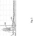
- Fig. 2 shows a waveform 810 of the first voltage (Vce) and a waveform 820 of a second voltage (Vge) during the switching off of the IGBT. Referring to Fig. 2 , the waveforms of the first and second voltage 810, 820 both oscillate severely, which may damage the IGBT.
- embodiments of the present disclosure relate to a protection circuit for a controllable switch which comprises a control terminal, a first terminal, and a second terminal having a lower electric potential than the first terminal.
- the protection device comprises an active clamping module and a damping module.
- the active clamping module is coupled between the first terminal and the control terminal of the controllable switch and configured to clamp a first voltage across the first terminal and the second terminal.
- the damping module is coupled to an output of the active clamping module and configured to damp oscillations of a second voltage across the control terminal and the second terminal.
- embodiments of the present disclosure relate to a protection method for a controllable switch which comprises a control terminal, a first terminal, and a second terminal having a lower electric potential than the first terminal.
- the protection method comprises clamping a first voltage across the first terminal and the second terminal by an active clamping module coupled between the first terminal and the control terminal of the controllable switch; and damping oscillation of a second voltage across the control terminal and the second terminal by a damping module coupled to an output of the active clamping module.
- Embodiments of the present disclosure relate to a protection circuit for a controllable switch, which can protect the controllable switch from over voltage and obtain good clamping behavior.
- Fig. 3 shows a sketch view of a protection circuit 100 in accordance with an exemplary embodiment of the present disclosure.
- the protection circuit 100 is coupled with a controllable switch 200 and configured to protect the controllable switch 200.
- the controllable switch 200 comprises a control terminal 201, a first terminal 203, and a second terminal 205, wherein the second terminal 205 has a lower electric potential than the first terminal 203.
- the controllable switch 200 may comprise at least one of an insulated gate bipolar transistor (IGBT) and a metal-oxide-semiconductor field effect transistor (MOSFET).
- the controllable switch 200 comprises an IGBT, and the control terminal 201, the first terminal 203 and the second terminal 205 are respectively a gate, a collector and an emitter of the IGBT.
- the controllable switch 200 comprises a MOSFET, the control terminal 201, the first terminal 203 and the second terminal 205 are respectively a gate, a drain and a source of the MOSFET.
- the protection circuit 100 comprises a gate driver 110, an active clamping module 120, a damping module 130 and a diode 140.
- the gate driver 110 is coupled to the control terminal 201 of the controllable switch 200 and configured to drive the controllable switch 200 by sending control signals to the control terminal 201.
- the active clamping module 120 is coupled between the first terminal 203 and the control terminal 201 of the controllable switch 200 and configured to clamp a first voltage across the first terminal 203 and the second terminal 205.
- the active clamping module 120 comprises at least one transient voltage suppressor (TVS).
- the damping module 130 is coupled to an output of the active clamping module 120 and configured to damp oscillations of a second voltage across the control terminal 201 and the second terminal 205.
- the damping module 130 comprises a filter, such as a band-pass filter or a low pass filter.
- the diode 140 is coupled between the output of the damping module and the control terminal 201 of the controllable switch 200, and configured to allow a current flowing from the damping module 130 to the control terminal 201 and prevent a current flowing from the control terminal 201 to the damping module 130.
- the diode 140 has a cathode coupled to the control terminal 201 of the controllable switch 200 and an anode coupled to the output of the damping module 130.
- Fig. 4 is a sketch view showing a protection circuit 300 in accordance with another exemplary embodiment of the present disclosure.
- the protection circuit 300 comprises a gate driver 310, an active clamping module 320, a damping module 330 and a diode 340.
- the gate driver 310 is coupled between the control terminal 201 and the second terminal 205 and comprises a voltage source 311 and a gate off resistor R3 which is coupled with the voltage source 311 in series.
- the active clamping module 320 coupled between the first terminal 203 and the control terminal 201 comprises a transient voltage suppressor (TVS) or a Zener diode, which has a cathode coupled with the first terminal 203 of the controllable switch 200 and an anode coupled with an input of the damping module 330.
- the active clamping module 320 is configured to clamp a first voltage across the first terminal 203 and the second terminal 205.
- the damping module comprises a low pass filter 330 and is configured to block highfrequency signals from the active clamping module 320, in order to damp oscillations of a second voltage across the control terminal 201 and the second terminal 205.
- the low pass filter 330 comprises a first resistor R1 and a first capacitor C1.
- the first resistor R1 is coupled between the first terminal 203 and the control terminal 201 of the controllable switch 200, and in series with the active clamping module 320.
- the first capacitor C1 is coupled between the control terminal 201 and the second terminal 205 of the controllable switch 200.
- the first resistor R1 has a first terminal coupled with the anode of the TVS 320 and a second terminal coupled with the control terminal via the diode 340.
- the first capacitor C1 has a first terminal coupled with the second terminal of the first resistor R1 and a second terminal coupled with the second terminal 205 of the controllable switch.
- the diode 340 has an anode coupled with a node between the first resistor R1 and the first capacitor C1, and a cathode coupled with the control terminal 201 of the controllable switch 200.
- Fig. 5 is a sketch view illustrating a waveform 910 of the first voltage and a waveform 920 of the second voltage during the switching off of a controllable switch which is protected by the protection circuit shown in Fig. 4 .
- the waveform of the second voltage 920 oscillates at first, but then tends to be stable.
- the waveform of the first voltage 910 is substantially stable during the switching off the controllable switch.
- the damping module reduces the oscillations and thus reduced risk of damage of the controllable switch.
- Fig. 6 is a sketch view showing a protection circuit 400 in accordance with another exemplary embodiment of the present disclosure.
- the protection circuit 400 comprises a gate driver 410, an active clamping module 420, a damping module 430 and a diode 440.
- the active clamping module 420 comprises a plurality of TVSs coupled in series between the first terminal 203 and the control terminal 201 of the controllable switch 200, and each TVS has a breakdown voltage.
- the active clamping module 420 provides a higher clamping threshold than the active clamping module with a single TVS, such as the active clamping module 320 shown in Fig. 4 , because the clamping threshold of the active clamping module 420 is equal to a sum of the breakdown voltages of all the TVSs.
- the plurality of TVSs start to work at the same time to clamp the first voltage.
- the gate driver 410, the damping module 430 and the diode 440 may be similar to the corresponding components of the protection circuit 100 and 300, description of which will not be repeated here.
- Fig. 7 is a sketch view showing a protection circuit 500 in accordance with another exemplary embodiment of the present disclosure.
- the protection circuit 500 comprises a gate driver 510, an active clamping module 520, a damping module 530, a diode 540 and a bypass module 550.
- the active clamping module 520 comprises a plurality of TVSs coupled in series between the first terminal 203 and the control terminal 201 of the controllable switch 200.
- the bypass module 550 is coupled in parallel with at least one of the plurality of TVSs, and configured to bypass the at least one of the plurality of TVSs (hereinafter referred to as a first part of TVSs) when a rising rate of the first voltage exceeds a pre-determined bypass threshold, in such a manner that the other TVS(s) not being bypassed (hereinafter referred to as a second part of TVSs) will start to work at first once the first voltage exceeds a first clamping threshold equal to a sum of breakdown voltages of the second part of TVSs, which is lower than a second clamping threshold (a sum of breakdown voltages of all TVSs) when all the TVSs are engaged.
- a first part of TVSs a pre-determined bypass threshold
- the bypass module 550 will not bypass the first part of TVSs anymore, and the first part of TVSs will start to work with the second part of TVSs together.
- no bypass module is coupled with the active clamping module 420 and thus all the TVSs start to work simultaneously when the first voltage exceeds the clamping threshold (the sum of the breakdown voltages of all TVSs).
- the clamping threshold the sum of the breakdown voltages of all TVSs.
- a part (the second part) of the TVSs in the active clamping module 520 starts to work before the first voltage exceeds that clamping threshold (the sum of the breakdown voltages of all TVSs). Therefore, the active clamping module 520 will start up earlier than the active clamping module 420 in Fig. 6 , so the startup of the active clamping module 520 is speeded up by using the bypass module 550.
- the active clamping module 520 comprises a first TVS 521 and a second TVS 522.
- the bypass module 550 is coupled in parallel with the first TVS 521, and the bypass module 550 comprises a second capacitor C2.
- the bypass threshold depends on a parameter of the second capacitor C2.
- the gate driver 510, the damping module 530 and the diode 540 may be similar to the corresponding components of the protection circuit 100 and 300, description of which will not be repeated here.
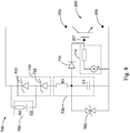
- Fig. 8 is a sketch view showing a protection circuit 700 in accordance with another exemplary embodiment of the present disclosure.
- the protection circuit 700 comprises a gate driver 710, an active clamping module 720 comprising two TVSs 721, 722, a damping module 730, a diode 740, a bypass module 750 and a voltage limiter 760.
- the gate driver 710, the active clamping module 720, the damping module 730 and the diode 740 may be similar to the corresponding components of the protection circuit 500, description of which will not be repeated here.
- the bypass module 750 comprises a second capacitor C2 and a second resistor R2 coupled in series with the second capacitor C2.
- the second capacitor C2 is configured to bypass a part of TVSs in the active clamping module 720, when a rising rate of the first voltage exceeds a pre-determined bypass threshold.
- the second resistor R2 is configured to limit a current flowing through the second capacitor C2 and the second resistor R2.
- the voltage limiter 760 is coupled between the control terminal 201 and the second terminal 205 of the controllable switch 200 and configured to limit a second voltage across the control terminal 201 and the second terminal 205 in a preset range. When the second voltage increases to a value exceeding the preset range, the voltage limiter 760 start to work to clamp the second voltage.
- the voltage limiter comprises a bilateral Zener diode 760 coupled between the control terminal 201 and the second terminal 205 of the controllable switch 200.
- the bilateral Zener diode 760 is configured to reset the second capacitor C2 of the bypass module 750 during the switching on of the controllable switch.
- the controllable switch When the controllable switch is working, it is turned on and off alternately for many times. During the switching off period, the second resistor R2 may be charged to bypass the TVS(s), and then when the controllable switch is turned on, the second capacitor C2 will be discharged in order to be reset before a next switching off period.
- the second capacitor C2 is discharged via the second resistor R2, the controllable switch 200, the bilateral Zener diode 760, the first resistance R1, and the TVS 722.
- a voltage across the second capacitor C2 is reset to an initial value, and the initial value depends on a breakdown voltage of the bilateral Zener diode 760 which is a fixed value. Therefore, the voltage across the second capacitor C2 will be the same every time after the discharging and before the next switching off period, which will help to enable consistent behavior of the bypass module.
- Embodiments of the present disclosure also relate to a protection method for a controllable switch, the controllable switch comprising a control terminal, a first terminal, and a second terminal having a lower electric potential than the first terminal.
- the method comprises clamping a first voltage across the first terminal and the second terminal by an active clamping module coupled between the first terminal and the control terminal of the controllable switch; and damping oscillations of a second voltage across the control terminal and the second terminal by a damping module coupled to an output of the active clamping module.
Landscapes
- Engineering & Computer Science (AREA)
- Power Engineering (AREA)
- Electronic Switches (AREA)
- Power Conversion In General (AREA)
Abstract
A protection circuit for a controllable switch comprising a control terminal, a first terminal, and a second terminal having a lower electric potential than the first terminal, the protection device comprising: an active clamping module, coupled between the first terminal and the control terminal of the controllable switch, configured to clamp a first voltage across the first terminal and the second terminal; and a damping module, coupled to an output of the active clamping module and configured to damp oscillations of a second voltage across the control terminal and the second terminal. Embodiments of the present disclosure also relate to a protection method for a controllable switch.
Description
- Embodiments of the present disclosure relate generally to protection circuits and methods for controllable switches.
- Controllable switches, such as insulated gate bipolar transistor (IGBT) and metal-oxide-semiconductor field-effect transistor (MOSFET) often encounter over voltage events at various working scenarios. The active voltage clamping (AVC) circuit is developed to solve this problem, which works as a close loop control system for the voltage across the controllable switch. However, in practice, the delay effect due to the characteristics of the controllable switch will have a negative impact on the close loop stability, which will cause unacceptable oscillations of the voltage.
-
Fig. 1 shows aconventional protection circuit 600 for a IGBT. Theprotection circuit 600 comprises anAVC circuit 620 and agate driver 610. TheAVC circuit 620 is coupled between a collector and a gate of the IGBT and configured to clamp a first voltage (Vce) across the collector and the emitter. Thegate driver 610 is coupled between a gate and the emitter of the IGBT.Fig. 2 shows awaveform 810 of the first voltage (Vce) and awaveform 820 of a second voltage (Vge) during the switching off of the IGBT. Referring toFig. 2 , the waveforms of the first andsecond voltage - Therefore, it is desirable to provide new protection circuits and methods for controllable switches to solve the above-mentioned problem.
- In one aspect, embodiments of the present disclosure relate to a protection circuit for a controllable switch which comprises a control terminal, a first terminal, and a second terminal having a lower electric potential than the first terminal. The protection device comprises an active clamping module and a damping module. The active clamping module is coupled between the first terminal and the control terminal of the controllable switch and configured to clamp a first voltage across the first terminal and the second terminal. The damping module is coupled to an output of the active clamping module and configured to damp oscillations of a second voltage across the control terminal and the second terminal.
- In another aspect, embodiments of the present disclosure relate to a protection method for a controllable switch which comprises a control terminal, a first terminal, and a second terminal having a lower electric potential than the first terminal. The protection method comprises clamping a first voltage across the first terminal and the second terminal by an active clamping module coupled between the first terminal and the control terminal of the controllable switch; and damping oscillation of a second voltage across the control terminal and the second terminal by a damping module coupled to an output of the active clamping module.
- These and other features, aspects, and advantages of the present disclosure will become better understood when the following detailed description is read with reference to the accompanying drawings in which like characters represent like parts throughout the drawings, wherein:
-
Fig. 1 is a sketch view of a conventional protection circuit; -
Fig. 2 is a sketch view illustrating waveforms of a first and second voltage during switching off of a controllable switch which is protected by the protection circuit shown inFig. 1 ; -
Fig. 3 is a sketch view of a protection circuit in accordance with an exemplary embodiment of the present disclosure; -
Fig. 4 is a sketch view of a protection circuit in accordance with another exemplary embodiment of the present disclosure; -
Fig. 5 is a sketch view illustrating waveforms of a first and second voltage during switching-off of a controllable switch which is protected by the protection circuit shown inFig. 4 ; -
Fig. 6 is a sketch view of a protection circuit in accordance with another exemplary embodiment of the present disclosure; -
Fig. 7 is a sketch view of a protection circuit in accordance with another exemplary embodiment of the present disclosure; and -
Fig. 8 is a sketch view of a protection circuit in accordance with another exemplary embodiment of the present disclosure. - In an effort to provide a concise description of these embodiments, not all features of an actual implementation are described in one or more specific embodiments. It should be appreciated that in the development of any such actual implementation, as in any engineering or design project, numerous implementation-specific decisions must be made to achieve the developers' specific goals, such as compliance with system-related and business-related constraints, which may vary from one implementation to another. Moreover, it should be appreciated that such a development effort might be complex and time consuming, but would nevertheless be a routine undertaking of design, fabrication, and manufacture for those of ordinary skill having the benefit of the present disclosure.
- Unless defined otherwise, technical and scientific terms used herein have the same meaning as is commonly understood by one of ordinary skill in the art to which the present disclosure belongs. The terms "first," "second," "third," "fourth," and the like, as used herein do not denote any order, quantity, or importance, but rather are used to distinguish one element from another. Also, the terms "a" and "an" do not denote a limitation of quantity, but rather denote the presence of at least one of the referenced items. The term "or" is meant to be inclusive and mean either any, several, or all of the listed items. The use of "including," "comprising," or "having," and variations thereof herein are meant to encompass the items listed thereafter and equivalents thereof as well as additional items.
- Embodiments of the present disclosure relate to a protection circuit for a controllable switch, which can protect the controllable switch from over voltage and obtain good clamping behavior.
-
Fig. 3 shows a sketch view of aprotection circuit 100 in accordance with an exemplary embodiment of the present disclosure. Theprotection circuit 100 is coupled with acontrollable switch 200 and configured to protect thecontrollable switch 200. Thecontrollable switch 200 comprises acontrol terminal 201, afirst terminal 203, and asecond terminal 205, wherein thesecond terminal 205 has a lower electric potential than thefirst terminal 203. - The
controllable switch 200 may comprise at least one of an insulated gate bipolar transistor (IGBT) and a metal-oxide-semiconductor field effect transistor (MOSFET). In some embodiments, thecontrollable switch 200 comprises an IGBT, and thecontrol terminal 201, thefirst terminal 203 and thesecond terminal 205 are respectively a gate, a collector and an emitter of the IGBT. In some other embodiments, thecontrollable switch 200 comprises a MOSFET, thecontrol terminal 201, thefirst terminal 203 and thesecond terminal 205 are respectively a gate, a drain and a source of the MOSFET. - Referring to
Fig. 3 , theprotection circuit 100 comprises agate driver 110, anactive clamping module 120, adamping module 130 and adiode 140. - The
gate driver 110 is coupled to thecontrol terminal 201 of thecontrollable switch 200 and configured to drive thecontrollable switch 200 by sending control signals to thecontrol terminal 201. - The
active clamping module 120 is coupled between thefirst terminal 203 and thecontrol terminal 201 of thecontrollable switch 200 and configured to clamp a first voltage across thefirst terminal 203 and thesecond terminal 205. In some embodiments, theactive clamping module 120 comprises at least one transient voltage suppressor (TVS). - The
damping module 130 is coupled to an output of theactive clamping module 120 and configured to damp oscillations of a second voltage across thecontrol terminal 201 and thesecond terminal 205. In some embodiments, thedamping module 130 comprises a filter, such as a band-pass filter or a low pass filter. - The
diode 140 is coupled between the output of the damping module and thecontrol terminal 201 of thecontrollable switch 200, and configured to allow a current flowing from thedamping module 130 to thecontrol terminal 201 and prevent a current flowing from thecontrol terminal 201 to thedamping module 130. In one embodiment, thediode 140 has a cathode coupled to thecontrol terminal 201 of thecontrollable switch 200 and an anode coupled to the output of thedamping module 130. -
Fig. 4 is a sketch view showing aprotection circuit 300 in accordance with another exemplary embodiment of the present disclosure. Theprotection circuit 300 comprises agate driver 310, anactive clamping module 320, adamping module 330 and adiode 340. - The
gate driver 310 is coupled between thecontrol terminal 201 and thesecond terminal 205 and comprises avoltage source 311 and a gate off resistor R3 which is coupled with thevoltage source 311 in series. - The
active clamping module 320 coupled between thefirst terminal 203 and thecontrol terminal 201 comprises a transient voltage suppressor (TVS) or a Zener diode, which has a cathode coupled with thefirst terminal 203 of thecontrollable switch 200 and an anode coupled with an input of thedamping module 330. Theactive clamping module 320 is configured to clamp a first voltage across thefirst terminal 203 and thesecond terminal 205. - The damping module comprises a
low pass filter 330 and is configured to block highfrequency signals from theactive clamping module 320, in order to damp oscillations of a second voltage across thecontrol terminal 201 and thesecond terminal 205. Specifically, thelow pass filter 330 comprises a first resistor R1 and a first capacitor C1. The first resistor R1 is coupled between thefirst terminal 203 and thecontrol terminal 201 of thecontrollable switch 200, and in series with theactive clamping module 320. The first capacitor C1 is coupled between thecontrol terminal 201 and thesecond terminal 205 of thecontrollable switch 200. - In the embodiment shown in
Fig. 4 , the first resistor R1 has a first terminal coupled with the anode of theTVS 320 and a second terminal coupled with the control terminal via thediode 340. The first capacitor C1 has a first terminal coupled with the second terminal of the first resistor R1 and a second terminal coupled with thesecond terminal 205 of the controllable switch. Thediode 340 has an anode coupled with a node between the first resistor R1 and the first capacitor C1, and a cathode coupled with thecontrol terminal 201 of thecontrollable switch 200. -
Fig. 5 is a sketch view illustrating awaveform 910 of the first voltage and awaveform 920 of the second voltage during the switching off of a controllable switch which is protected by the protection circuit shown inFig. 4 . Referring toFig. 5 , the waveform of thesecond voltage 920 oscillates at first, but then tends to be stable. The waveform of thefirst voltage 910 is substantially stable during the switching off the controllable switch. Compared to the waveforms inFig. 2 , the damping module reduces the oscillations and thus reduced risk of damage of the controllable switch. -
Fig. 6 is a sketch view showing aprotection circuit 400 in accordance with another exemplary embodiment of the present disclosure. Theprotection circuit 400 comprises agate driver 410, anactive clamping module 420, a dampingmodule 430 and adiode 440. - The
active clamping module 420 comprises a plurality of TVSs coupled in series between thefirst terminal 203 and thecontrol terminal 201 of thecontrollable switch 200, and each TVS has a breakdown voltage. Theactive clamping module 420 provides a higher clamping threshold than the active clamping module with a single TVS, such as theactive clamping module 320 shown inFig. 4 , because the clamping threshold of theactive clamping module 420 is equal to a sum of the breakdown voltages of all the TVSs. When the first voltage exceeds the clamping threshold, the plurality of TVSs start to work at the same time to clamp the first voltage. - The
gate driver 410, the dampingmodule 430 and thediode 440 may be similar to the corresponding components of theprotection circuit -
Fig. 7 is a sketch view showing aprotection circuit 500 in accordance with another exemplary embodiment of the present disclosure. Theprotection circuit 500 comprises agate driver 510, anactive clamping module 520, a dampingmodule 530, adiode 540 and abypass module 550. - The
active clamping module 520 comprises a plurality of TVSs coupled in series between thefirst terminal 203 and thecontrol terminal 201 of thecontrollable switch 200. - The
bypass module 550 is coupled in parallel with at least one of the plurality of TVSs, and configured to bypass the at least one of the plurality of TVSs (hereinafter referred to as a first part of TVSs) when a rising rate of the first voltage exceeds a pre-determined bypass threshold, in such a manner that the other TVS(s) not being bypassed (hereinafter referred to as a second part of TVSs) will start to work at first once the first voltage exceeds a first clamping threshold equal to a sum of breakdown voltages of the second part of TVSs, which is lower than a second clamping threshold (a sum of breakdown voltages of all TVSs) when all the TVSs are engaged. After the second part of TVSs start to clamp the first voltage, the rising rate of the first voltage will decrease because of the clamping. Subsequently, thebypass module 550 will not bypass the first part of TVSs anymore, and the first part of TVSs will start to work with the second part of TVSs together. - In the embodiment shown in
Fig. 6 , no bypass module is coupled with theactive clamping module 420 and thus all the TVSs start to work simultaneously when the first voltage exceeds the clamping threshold (the sum of the breakdown voltages of all TVSs). However, in the embodiment shown inFig. 7 , a part (the second part) of the TVSs in theactive clamping module 520 starts to work before the first voltage exceeds that clamping threshold (the sum of the breakdown voltages of all TVSs). Therefore, theactive clamping module 520 will start up earlier than theactive clamping module 420 inFig. 6 , so the startup of theactive clamping module 520 is speeded up by using thebypass module 550. - In the embodiment shown in
Fig. 7 , theactive clamping module 520 comprises afirst TVS 521 and asecond TVS 522. Thebypass module 550 is coupled in parallel with thefirst TVS 521, and thebypass module 550 comprises a second capacitor C2. The bypass threshold depends on a parameter of the second capacitor C2. When the first voltage increases in a rising rate higher than the bypass threshold, thefirst TVS 521 will be bypassed by thebypass module 550, and thesecond TVS 522 will clamp the first voltage when the first voltage increases to a breakdown voltage of thesecond TVS 522. Then, the rising rate of the first voltage decreases, and thefirst TVS 521 will start to work. - The
gate driver 510, the dampingmodule 530 and thediode 540 may be similar to the corresponding components of theprotection circuit -
Fig. 8 is a sketch view showing aprotection circuit 700 in accordance with another exemplary embodiment of the present disclosure. Theprotection circuit 700 comprises agate driver 710, anactive clamping module 720 comprising twoTVSs module 730, adiode 740, abypass module 750 and avoltage limiter 760. - The
gate driver 710, theactive clamping module 720, the dampingmodule 730 and thediode 740 may be similar to the corresponding components of theprotection circuit 500, description of which will not be repeated here. - The
bypass module 750 comprises a second capacitor C2 and a second resistor R2 coupled in series with the second capacitor C2. The second capacitor C2 is configured to bypass a part of TVSs in theactive clamping module 720, when a rising rate of the first voltage exceeds a pre-determined bypass threshold. The second resistor R2 is configured to limit a current flowing through the second capacitor C2 and the second resistor R2. - The
voltage limiter 760 is coupled between thecontrol terminal 201 and thesecond terminal 205 of thecontrollable switch 200 and configured to limit a second voltage across thecontrol terminal 201 and thesecond terminal 205 in a preset range. When the second voltage increases to a value exceeding the preset range, thevoltage limiter 760 start to work to clamp the second voltage. - In some embodiments, the voltage limiter comprises a
bilateral Zener diode 760 coupled between thecontrol terminal 201 and thesecond terminal 205 of thecontrollable switch 200. Thebilateral Zener diode 760 is configured to reset the second capacitor C2 of thebypass module 750 during the switching on of the controllable switch. - When the controllable switch is working, it is turned on and off alternately for many times. During the switching off period, the second resistor R2 may be charged to bypass the TVS(s), and then when the controllable switch is turned on, the second capacitor C2 will be discharged in order to be reset before a next switching off period. The second capacitor C2 is discharged via the second resistor R2, the
controllable switch 200, thebilateral Zener diode 760, the first resistance R1, and theTVS 722. After the discharging is finished, a voltage across the second capacitor C2 is reset to an initial value, and the initial value depends on a breakdown voltage of thebilateral Zener diode 760 which is a fixed value. Therefore, the voltage across the second capacitor C2 will be the same every time after the discharging and before the next switching off period, which will help to enable consistent behavior of the bypass module. - Embodiments of the present disclosure also relate to a protection method for a controllable switch, the controllable switch comprising a control terminal, a first terminal, and a second terminal having a lower electric potential than the first terminal.
- The method comprises clamping a first voltage across the first terminal and the second terminal by an active clamping module coupled between the first terminal and the control terminal of the controllable switch; and damping oscillations of a second voltage across the control terminal and the second terminal by a damping module coupled to an output of the active clamping module.
- As will be understood by those familiar with the art, the present disclosure may be embodied in other specific forms without depending from the spirit or essential characteristics thereof. Accordingly, the disclosures and descriptions herein are intended to be illustrative, but not limiting, of the scope of the disclosure which is set forth in the following claims.
Claims (14)
- A protection circuit for a controllable switch comprising a control terminal, a first terminal, and a second terminal having a lower electric potential than the first terminal, the protection circuit comprising:an active clamping module, coupled between the first terminal and the control terminal of the controllable switch, configured to clamp a first voltage across the first terminal and the second terminal; anda damping module, coupled to an output of the active clamping module and configured to damp oscillations of a second voltage across the control terminal and the second terminal.
- The circuit according to claim 1, wherein the damping module comprises a filter.
- The circuit according to claim 2, wherein the filter comprises a band-pass filter.
- The circuit according to claim 2, wherein the filter comprises a low pass filter, the low pass filter comprising:a first resistor coupled between the first terminal and the control terminal of the controllable switch, and in series with the active clamping module; anda first capacitor coupled between the control terminal and the second terminal of the controllable switch.
- The circuit according to claim 1, wherein the active clamping module comprises at least one transient voltage suppressor (TVS).
- The circuit according to claim 1, wherein the active clamping module comprises a plurality of TVSs coupled in series between the first terminal and the control terminal of the controllable switch.
- The circuit according to claim 6, further comprising a bypass module coupled in parallel with at least one of the plurality of TVSs, and configured to bypass the at least one of the plurality of TVSs when a rising rate of the first voltage exceeds a pre-determined bypass threshold.
- The circuit according to claim 7, wherein the bypass module comprises a second capacitor.
- The circuit according to claim 1, further comprising a voltage limiter coupled between the control terminal and the second terminal of the controllable switch.
- The circuit according to claim 9, wherein the voltage limiter comprises a bilateral Zener diode.
- The circuit according to claim 1, wherein the controllable switch comprises at least one of an insulated gate bipolar transistor and a metal-oxide-semiconductor field effect transistor.
- The circuit according to claim 1, further comprising a diode having a cathode coupled to the control terminal of the controllable switch and an anode coupled to an output of the damping module.
- The circuit according to claim 1, further comprising: a gate driver, coupled to the control terminal of the controllable switch and configured to drive the controllable switch.
- A protection method for a controllable switch comprising a control terminal, a first terminal, and a second terminal having a lower electric potential than the first terminal, the protection method comprising:clamping a first voltage across the first terminal and the second terminal by an active clamping module coupled between the first terminal and the control terminal of the controllable switch; anddamping oscillation of a second voltage across the control terminal and the second terminal by a damping module coupled to an output of the active clamping module.
Applications Claiming Priority (1)
| Application Number | Priority Date | Filing Date | Title |
|---|---|---|---|
| CN201810002039.5A CN109995001A (en) | 2018-01-02 | 2018-01-02 | For protecting protection circuit and the guard method of controllable switch |
Publications (1)
| Publication Number | Publication Date |
|---|---|
| EP3506506A1 true EP3506506A1 (en) | 2019-07-03 |
Family
ID=64745998
Family Applications (1)
| Application Number | Title | Priority Date | Filing Date |
|---|---|---|---|
| EP18213755.4A Withdrawn EP3506506A1 (en) | 2018-01-02 | 2018-12-18 | Protection circuit and method for controllable switch |
Country Status (3)
| Country | Link |
|---|---|
| US (1) | US20190207598A1 (en) |
| EP (1) | EP3506506A1 (en) |
| CN (1) | CN109995001A (en) |
Families Citing this family (2)
| Publication number | Priority date | Publication date | Assignee | Title |
|---|---|---|---|---|
| DE102021207110B4 (en) * | 2021-07-07 | 2024-06-27 | Siemens Aktiengesellschaft | Arrangement and method for automatic configuration of a magnetic drive |
| US12132471B2 (en) * | 2022-08-12 | 2024-10-29 | Hamilton Sundstrand Corporation | Lightning protection for power MOSFETs |
Citations (3)
| Publication number | Priority date | Publication date | Assignee | Title |
|---|---|---|---|---|
| US20040075103A1 (en) * | 2001-10-09 | 2004-04-22 | Rainer Topp | Semiconductor circuit, especially for ignition purposes, and the use of the same |
| US20130155560A1 (en) * | 2011-12-14 | 2013-06-20 | Fuji Electric Co., Ltd. | Semiconductor Device |
| DE202014105631U1 (en) * | 2014-11-21 | 2014-12-09 | Infineon Technologies Ag | Circuit arrangement for reducing overvoltages |
Family Cites Families (4)
| Publication number | Priority date | Publication date | Assignee | Title |
|---|---|---|---|---|
| US5091817A (en) * | 1984-12-03 | 1992-02-25 | General Electric Company | Autonomous active clamp circuit |
| CN100574031C (en) * | 2007-04-06 | 2009-12-23 | 广州金升阳科技有限公司 | A kind of power convertor output protection circuit |
| CN202978213U (en) * | 2012-12-03 | 2013-06-05 | 广西柳工机械股份有限公司 | Power supply overvoltage protection circuit |
| CN107046361A (en) * | 2016-12-30 | 2017-08-15 | 江苏中科君芯科技有限公司 | IGBT dynamic active clamping protective circuits |
-
2018
- 2018-01-02 CN CN201810002039.5A patent/CN109995001A/en active Pending
- 2018-12-18 EP EP18213755.4A patent/EP3506506A1/en not_active Withdrawn
- 2018-12-18 US US16/223,514 patent/US20190207598A1/en not_active Abandoned
Patent Citations (3)
| Publication number | Priority date | Publication date | Assignee | Title |
|---|---|---|---|---|
| US20040075103A1 (en) * | 2001-10-09 | 2004-04-22 | Rainer Topp | Semiconductor circuit, especially for ignition purposes, and the use of the same |
| US20130155560A1 (en) * | 2011-12-14 | 2013-06-20 | Fuji Electric Co., Ltd. | Semiconductor Device |
| DE202014105631U1 (en) * | 2014-11-21 | 2014-12-09 | Infineon Technologies Ag | Circuit arrangement for reducing overvoltages |
Also Published As
| Publication number | Publication date |
|---|---|
| CN109995001A (en) | 2019-07-09 |
| US20190207598A1 (en) | 2019-07-04 |
Similar Documents
| Publication | Publication Date | Title |
|---|---|---|
| CN105939151B (en) | Electronic circuit | |
| JP6402591B2 (en) | Semiconductor device | |
| US7368972B2 (en) | Power transistor control device | |
| US10122274B2 (en) | Multi-function power control circuit using enhancement mode gallium nitride (GaN) high electron mobility transistors (HEMTs) | |
| CN109698684B (en) | Driving circuit for switch | |
| EP2801153B1 (en) | Apparatus and method for control of semiconductor switching devices | |
| CN109309381B (en) | Current limiting circuit and current limiting method | |
| JP2014512765A (en) | Cascade switch including normally-off device and normally-on device, and circuit including the switch | |
| US7053678B2 (en) | Driving circuit for a control terminal of a bipolar transistor in an emitter-switching configuration and corresponding method for reducing the VCESAT dynamic phenomenon | |
| CN114667681B (en) | Gate drive circuit | |
| EP3506506A1 (en) | Protection circuit and method for controllable switch | |
| CN112821723A (en) | Driver circuit for voltage-controlled power semiconductor elements | |
| JP2018007201A (en) | Gate driving circuit | |
| JP5034919B2 (en) | Temperature sensor circuit | |
| CN204597470U (en) | For reducing the circuit arrangement of overvoltage | |
| GB2053606A (en) | Improvements in and relating to semiconductor switching circuits | |
| CN209948951U (en) | Miller clamp circuit and power electronic device | |
| US20250150072A1 (en) | High Side Switch Gate Drive Apparatus and Control Method | |
| JP7177714B2 (en) | power supply | |
| CN117220480B (en) | A protection circuit for a power device and a driving method thereof, and a power supply device | |
| JP2025521875A (en) | Power Switch Short-Circuit Protection | |
| WO2022153521A1 (en) | Semiconductor power conversion device | |
| US10451665B2 (en) | Pulse current application circuit and control method thereof | |
| EP4525306A1 (en) | Protection structure for an enhancement-mode fet of a circuit and corresponding method | |
| CN121420461A (en) | Semiconductor protection devices and power conversion devices |
Legal Events
| Date | Code | Title | Description |
|---|---|---|---|
| PUAI | Public reference made under article 153(3) epc to a published international application that has entered the european phase |
Free format text: ORIGINAL CODE: 0009012 |
|
| STAA | Information on the status of an ep patent application or granted ep patent |
Free format text: STATUS: THE APPLICATION HAS BEEN PUBLISHED |
|
| AK | Designated contracting states |
Kind code of ref document: A1 Designated state(s): AL AT BE BG CH CY CZ DE DK EE ES FI FR GB GR HR HU IE IS IT LI LT LU LV MC MK MT NL NO PL PT RO RS SE SI SK SM TR |
|
| AX | Request for extension of the european patent |
Extension state: BA ME |
|
| STAA | Information on the status of an ep patent application or granted ep patent |
Free format text: STATUS: THE APPLICATION IS DEEMED TO BE WITHDRAWN |
|
| 18D | Application deemed to be withdrawn |
Effective date: 20200104 |