EP3506325B1 - Mehrschichtiger stapel umfassend leitfähige polymerschichten mit verbesserter leitfähigkeit und stabilität und verfahren zur herstellung davon - Google Patents
Mehrschichtiger stapel umfassend leitfähige polymerschichten mit verbesserter leitfähigkeit und stabilität und verfahren zur herstellung davon Download PDFInfo
- Publication number
- EP3506325B1 EP3506325B1 EP18212660.7A EP18212660A EP3506325B1 EP 3506325 B1 EP3506325 B1 EP 3506325B1 EP 18212660 A EP18212660 A EP 18212660A EP 3506325 B1 EP3506325 B1 EP 3506325B1
- Authority
- EP
- European Patent Office
- Prior art keywords
- conductive polymer
- layer
- layers
- multilayer stack
- polymer layer
- Prior art date
- Legal status (The legal status is an assumption and is not a legal conclusion. Google has not performed a legal analysis and makes no representation as to the accuracy of the status listed.)
- Active
Links
Images


Classifications
-
- H—ELECTRICITY
- H01—ELECTRIC ELEMENTS
- H01B—CABLES; CONDUCTORS; INSULATORS; SELECTION OF MATERIALS FOR THEIR CONDUCTIVE, INSULATING OR DIELECTRIC PROPERTIES
- H01B1/00—Conductors or conductive bodies characterised by the conductive materials; Selection of materials as conductors
- H01B1/06—Conductors or conductive bodies characterised by the conductive materials; Selection of materials as conductors mainly consisting of other non-metallic substances
- H01B1/12—Conductors or conductive bodies characterised by the conductive materials; Selection of materials as conductors mainly consisting of other non-metallic substances organic substances
- H01B1/124—Intrinsically conductive polymers
- H01B1/127—Intrinsically conductive polymers comprising five-membered aromatic rings in the main chain, e.g. polypyrroles, polythiophenes
-
- H—ELECTRICITY
- H01—ELECTRIC ELEMENTS
- H01B—CABLES; CONDUCTORS; INSULATORS; SELECTION OF MATERIALS FOR THEIR CONDUCTIVE, INSULATING OR DIELECTRIC PROPERTIES
- H01B1/00—Conductors or conductive bodies characterised by the conductive materials; Selection of materials as conductors
- H01B1/06—Conductors or conductive bodies characterised by the conductive materials; Selection of materials as conductors mainly consisting of other non-metallic substances
- H01B1/12—Conductors or conductive bodies characterised by the conductive materials; Selection of materials as conductors mainly consisting of other non-metallic substances organic substances
- H01B1/121—Charge-transfer complexes
-
- H—ELECTRICITY
- H01—ELECTRIC ELEMENTS
- H01B—CABLES; CONDUCTORS; INSULATORS; SELECTION OF MATERIALS FOR THEIR CONDUCTIVE, INSULATING OR DIELECTRIC PROPERTIES
- H01B1/00—Conductors or conductive bodies characterised by the conductive materials; Selection of materials as conductors
- H01B1/20—Conductive material dispersed in non-conductive organic material
- H01B1/22—Conductive material dispersed in non-conductive organic material the conductive material comprising metals or alloys
-
- H—ELECTRICITY
- H01—ELECTRIC ELEMENTS
- H01B—CABLES; CONDUCTORS; INSULATORS; SELECTION OF MATERIALS FOR THEIR CONDUCTIVE, INSULATING OR DIELECTRIC PROPERTIES
- H01B1/00—Conductors or conductive bodies characterised by the conductive materials; Selection of materials as conductors
- H01B1/20—Conductive material dispersed in non-conductive organic material
- H01B1/24—Conductive material dispersed in non-conductive organic material the conductive material comprising carbon-silicon compounds, carbon or silicon
-
- H—ELECTRICITY
- H01—ELECTRIC ELEMENTS
- H01B—CABLES; CONDUCTORS; INSULATORS; SELECTION OF MATERIALS FOR THEIR CONDUCTIVE, INSULATING OR DIELECTRIC PROPERTIES
- H01B3/00—Insulators or insulating bodies characterised by the insulating materials; Selection of materials for their insulating or dielectric properties
- H01B3/002—Inhomogeneous material in general
- H01B3/004—Inhomogeneous material in general with conductive additives or conductive layers
-
- H—ELECTRICITY
- H01—ELECTRIC ELEMENTS
- H01B—CABLES; CONDUCTORS; INSULATORS; SELECTION OF MATERIALS FOR THEIR CONDUCTIVE, INSULATING OR DIELECTRIC PROPERTIES
- H01B7/00—Insulated conductors or cables characterised by their form
- H01B7/02—Disposition of insulation
-
- H—ELECTRICITY
- H01—ELECTRIC ELEMENTS
- H01C—RESISTORS
- H01C1/00—Details
- H01C1/16—Resistor networks not otherwise provided for
-
- H—ELECTRICITY
- H01—ELECTRIC ELEMENTS
- H01C—RESISTORS
- H01C17/00—Apparatus or processes specially adapted for manufacturing resistors
- H01C17/06—Apparatus or processes specially adapted for manufacturing resistors adapted for coating resistive material on a base
-
- H—ELECTRICITY
- H01—ELECTRIC ELEMENTS
- H01C—RESISTORS
- H01C17/00—Apparatus or processes specially adapted for manufacturing resistors
- H01C17/06—Apparatus or processes specially adapted for manufacturing resistors adapted for coating resistive material on a base
- H01C17/065—Apparatus or processes specially adapted for manufacturing resistors adapted for coating resistive material on a base by thick film techniques, e.g. serigraphy
- H01C17/06506—Precursor compositions therefor, e.g. pastes, inks, glass frits or green body
- H01C17/06573—Precursor compositions therefor, e.g. pastes, inks, glass frits or green body characterised by the permanent binder
- H01C17/06586—Precursor compositions therefor, e.g. pastes, inks, glass frits or green body characterised by the permanent binder composed of organic material
-
- H—ELECTRICITY
- H01—ELECTRIC ELEMENTS
- H01C—RESISTORS
- H01C17/00—Apparatus or processes specially adapted for manufacturing resistors
- H01C17/22—Apparatus or processes specially adapted for manufacturing resistors adapted for trimming
- H01C17/24—Apparatus or processes specially adapted for manufacturing resistors adapted for trimming by removing or adding resistive material
-
- H—ELECTRICITY
- H01—ELECTRIC ELEMENTS
- H01C—RESISTORS
- H01C17/00—Apparatus or processes specially adapted for manufacturing resistors
- H01C17/22—Apparatus or processes specially adapted for manufacturing resistors adapted for trimming
- H01C17/26—Apparatus or processes specially adapted for manufacturing resistors adapted for trimming by converting resistive material
- H01C17/265—Apparatus or processes specially adapted for manufacturing resistors adapted for trimming by converting resistive material by chemical or thermal treatment, e.g. oxydation, reduction, annealing
-
- H—ELECTRICITY
- H01—ELECTRIC ELEMENTS
- H01C—RESISTORS
- H01C7/00—Non-adjustable resistors formed as one or more layers or coatings; Non-adjustable resistors made from powdered conducting material or powdered semi-conducting material with or without insulating material
- H01C7/001—Mass resistors
-
- H—ELECTRICITY
- H01—ELECTRIC ELEMENTS
- H01C—RESISTORS
- H01C7/00—Non-adjustable resistors formed as one or more layers or coatings; Non-adjustable resistors made from powdered conducting material or powdered semi-conducting material with or without insulating material
- H01C7/003—Thick film resistors
- H01C7/005—Polymer thick films
-
- H—ELECTRICITY
- H01—ELECTRIC ELEMENTS
- H01C—RESISTORS
- H01C7/00—Non-adjustable resistors formed as one or more layers or coatings; Non-adjustable resistors made from powdered conducting material or powdered semi-conducting material with or without insulating material
- H01C7/18—Non-adjustable resistors formed as one or more layers or coatings; Non-adjustable resistors made from powdered conducting material or powdered semi-conducting material with or without insulating material comprising a plurality of layers stacked between terminals
-
- H—ELECTRICITY
- H05—ELECTRIC TECHNIQUES NOT OTHERWISE PROVIDED FOR
- H05B—ELECTRIC HEATING; ELECTRIC LIGHT SOURCES NOT OTHERWISE PROVIDED FOR; CIRCUIT ARRANGEMENTS FOR ELECTRIC LIGHT SOURCES, IN GENERAL
- H05B3/00—Ohmic-resistance heating
- H05B3/10—Heating elements characterised by the composition or nature of the materials or by the arrangement of the conductor
- H05B3/12—Heating elements characterised by the composition or nature of the materials or by the arrangement of the conductor characterised by the composition or nature of the conductive material
- H05B3/14—Heating elements characterised by the composition or nature of the materials or by the arrangement of the conductor characterised by the composition or nature of the conductive material the material being non-metallic
- H05B3/146—Conductive polymers, e.g. polyethylene, thermoplastics
-
- B—PERFORMING OPERATIONS; TRANSPORTING
- B64—AIRCRAFT; AVIATION; COSMONAUTICS
- B64D—EQUIPMENT FOR FITTING IN OR TO AIRCRAFT; FLIGHT SUITS; PARACHUTES; ARRANGEMENT OR MOUNTING OF POWER PLANTS OR PROPULSION TRANSMISSIONS IN AIRCRAFT
- B64D15/00—De-icing or preventing icing on exterior surfaces of aircraft
- B64D15/12—De-icing or preventing icing on exterior surfaces of aircraft by electric heating
-
- B—PERFORMING OPERATIONS; TRANSPORTING
- B64—AIRCRAFT; AVIATION; COSMONAUTICS
- B64D—EQUIPMENT FOR FITTING IN OR TO AIRCRAFT; FLIGHT SUITS; PARACHUTES; ARRANGEMENT OR MOUNTING OF POWER PLANTS OR PROPULSION TRANSMISSIONS IN AIRCRAFT
- B64D45/00—Aircraft indicators or protectors not otherwise provided for
- B64D45/02—Lightning protectors; Static dischargers
-
- H—ELECTRICITY
- H01—ELECTRIC ELEMENTS
- H01C—RESISTORS
- H01C1/00—Details
- H01C1/14—Terminals or tapping points specially adapted for resistors; Arrangements of terminals or tapping points on resistors
- H01C1/142—Terminals or tapping points specially adapted for resistors; Arrangements of terminals or tapping points on resistors the terminals or tapping points being coated on the resistive element
-
- H—ELECTRICITY
- H01—ELECTRIC ELEMENTS
- H01C—RESISTORS
- H01C17/00—Apparatus or processes specially adapted for manufacturing resistors
- H01C17/28—Apparatus or processes specially adapted for manufacturing resistors adapted for applying terminals
-
- H—ELECTRICITY
- H01—ELECTRIC ELEMENTS
- H01C—RESISTORS
- H01C7/00—Non-adjustable resistors formed as one or more layers or coatings; Non-adjustable resistors made from powdered conducting material or powdered semi-conducting material with or without insulating material
- H01C7/02—Non-adjustable resistors formed as one or more layers or coatings; Non-adjustable resistors made from powdered conducting material or powdered semi-conducting material with or without insulating material having positive temperature coefficient
- H01C7/028—Non-adjustable resistors formed as one or more layers or coatings; Non-adjustable resistors made from powdered conducting material or powdered semi-conducting material with or without insulating material having positive temperature coefficient consisting of organic substances
-
- H—ELECTRICITY
- H05—ELECTRIC TECHNIQUES NOT OTHERWISE PROVIDED FOR
- H05B—ELECTRIC HEATING; ELECTRIC LIGHT SOURCES NOT OTHERWISE PROVIDED FOR; CIRCUIT ARRANGEMENTS FOR ELECTRIC LIGHT SOURCES, IN GENERAL
- H05B2214/00—Aspects relating to resistive heating, induction heating and heating using microwaves, covered by groups H05B3/00, H05B6/00
- H05B2214/02—Heaters specially designed for de-icing or protection against icing
Definitions
- the present disclosure relates generally to methods for forming multilayer stacks and devices comprising multilayer stacks.
- the disclosure further relates to enhancing conductivity of a polymer More particularly the present disclosure relates to stacking up layers of a conductive polymer interposed between, or separated by, insulating layers to enhance conductivity and achieve a particular conductivity level and a particular electrical resistance level.
- US 2007/0210073 A1 states a composite ice protection heater for an aircraft.
- the composite heater includes at least one electrically insulating layer, and at least one electric heater element comprising an electrically conductive layer bonded to the insulating layer.
- the conductive layer may include a pre-impregnated woven fabric that includes a plurality of threads that include an electrically conductive material, such as carbon or graphite fibers.
- the composite heater can be incorporated into a composite surface structure of an aircraft.
- the conductive layer and insulating layer may include a plurality of spaced openings through the layers that cooperate with an underlying open-cell matrix to attenuate noise at the associated surface of an aircraft.
- a desired electrical resistance of the conductive layer may be obtained by introducing a plurality of discontinuities in the layer, such as spaced holes or slits.
- the conductive polymer may be brittle and not suitable to some applications. To make the conductive polymer usable in particular applications, it is first rendered flexible and compatible with other materials by, for example, formulating the conductive polymer in polyurethane, epoxy, or phenoxy resins, among other example resins. Formulating conductive polymer in a resin may, for example, involve dispersing the conductive polymer in the resin to form a network of the conductive polymer therein.
- the present disclosure describes examples that relate to multilayer stack with enhanced conductivity and stability. In one aspect, the present disclosure describes a method as defined in claim 1.
- the present disclosure describes a device as defined in claim 13.
- the present disclosure describes a component of a vehicle such as an aircraft.
- the component includes a multilayer stack of conductive polymer layers and insulating layers disposed on or proximate to a surface of the component.
- the multilayer stack includes a plurality of conductive polymer layers, each conductive polymer layer being interposed between respective insulating layers.
- Each conductive polymer layer has a respective electrical resistance, such that when the respective conductive polymer layers are connected in parallel to a power source coupled to the aircraft, a resultant electrical resistance of the respective conductive polymer layers is less than each respective electrical resistance.
- Formulating a conductive polymer in an insulating material such as resin reduces or degrades electrical conductivity of the conductive polymer despite treatment with a conductivity enhancer such as isopropanol (IPA). Such reduction or degradation in electrical conductivity may be undesirable.
- a multilayer stack having a conductive polymer layer treated with a conductivity enhancer and "sandwiched" or interposed between two insulating layers.
- An example process disclosed herein involves casting and curing a film of an insulating material such as resin (e.g., polyurethane (PUR)) followed by applying a coating of conductive polymer.
- the conductive polymer can then be treated with a conductivity enhancer to increase electrical conductivity of the conductive polymer layer.
- the treated conductive polymer layer may then be dried, and another insulating layer is applied and cured.
- This layer-by-layer stack-up provides a protective encapsulation of the conductive polymer from the environment and maintains the level of electrical conductivity of the conductive polymer layer.
- this process allows for forming a multilayer stack of conductive polymer layers and can lower overall electrical resistance of the multilayer stack.
- the electrical resistance decreases per Ohm's law.
- a multilayer stack of conductive polymer layers interposed between insulation layers can be fabricated to have a particular electrical resistance.
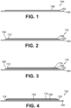
- Figures 1-5 illustrate stages of fabricating a multilayer stack, in accordance with an example implementation.
- the illustrations shown in Figures 1-5 are generally shown in cross-sectional views to illustrate sequentially formed layers developed to create the multilayer stack.
- the layers can be developed by microfabrication and/or manufacturing techniques such as, for example, electroplating, photolithography, deposition, and/or evaporation fabrication processes, spin coating, spray coating, roll-to-roll coating, ink jet, direct-write, among other possible deposition or forming techniques.
- the various materials of the layers may be formed according to patterns using photoresists and/or masks to pattern materials in particular arrangements.
- electroplating techniques can also be employed to coat ends or edges of conductive polymer layers with electrical contacts (e.g., metallic pads or electrical leads).
- electrical contacts e.g., metallic pads or electrical leads.
- an arrangement of conductive material formed by a deposition and/or photolithography process can be plated with a metallic material to create a conductive electrical contact.
- Figure 1 illustrates a substrate 100 with an insulating layer 102 formed on the substrate 100 to provide a partially-fabricated multilayer stack 104, in accordance with an example implementation.
- the insulating layer 102 can adhere to the substrate 100.
- the insulating layer 102 can be configured to facilitate forming a conductive polymer layer thereon, such that the conductive polymer layer adheres to the insulating layer 102.
- the substrate 100 can be made out of an epoxy resin, a composite structural material (e.g., of a wing, blade, or any component of an aircraft), thermoplastic resin, thermoset material, a polycarbonate material, etc.
- the substrate 100 can be cleaned before forming the insulating layer 102.
- the substrate 100 may be cleaned in a variety of ways such as soaking in a first fluid, rinsing with a second fluid, and drying with a gas.
- the first fluid can include a solvent, such as acetone.
- the second fluid can include isopropyl alcohol.
- the gas can include nitrogen. Rinsing may be performed in a variety ways, such as soaking in a bath in a tank, an automated spray, manually via a squirt bottle, etc.
- the substrate 100 can be baked before forming the insulating layer 102.
- the substrate 100 may be baked at a particular temperature for a time period.
- the temperature can be 90 degrees Celsius (C) and the time period may be 2 minutes.
- the substrate 100 can be plasma cleaned before forming the insulating layer 102.
- the substrate 100 may be plasma-cleaned at a particular power level for a time period.
- the insulating layer 102 can be formed, for example, of a resin material.
- Example resin materials include epoxy, thermoplastic resins, phenolic resins, or silicone resins, which are characterized in being durable and operable under elevated temperatures. It may be desirable to configure the insulating layer 102 of a thermostable resin material.
- the insulating layer 102 can be made of PUR, which is a polymer composed of organic units joined by carbamate (urethane) links.
- PUR can be a thermosetting polymer or a thermoplastic polymer.
- PUR can be formed by reacting a di- or poly-isocyanate with a polyol. PUR is described herein as an example for illustration, and other types of resin could be used to make the insulating layer 102.
- the insulating layer 102 can be deposited on the substrate 100 in a variety of ways such as brushing, painting, patterning, printing, any additive manufacturing method, etc.
- the insulating layer 102 may be cured (e.g., cured at a particular temperature such as 70 C). Curing may involve toughening or hardening of the insulating material by heat or chemical additives, among other processes. Curing can be partial or can be full depending on the application and implementation.
- the insulating layer 102 can have a surface 106 configured to receive a conductive polymer layer as described next.
- the conductive polymer layer 108 could be made of an intrinsically conducting polymer (ICP). ICPs include synthetic organic polymers configured to conduct electricity. In other examples, the conductive polymer layer 108 could be made of an extrinsically conducting polymer. An extrinsically conducting polymer is obtained by adding specific additives (e.g., metallic particle fillers) to a naturally insulating polymer to render such an insulting polymer electrically conductive.
- ICPs intrinsically conducting polymer
- An extrinsically conducting polymer is obtained by adding specific additives (e.g., metallic particle fillers) to a naturally insulating polymer to render such an insulting polymer electrically conductive.
- the conductive polymer can be produced by an emulsion polymerization method to form an organically soluble conductive polymer.
- the organically soluble conductive polymer can then be mixed with toluene, for example.
- Toluene is a colorless, water-insoluble liquid that operates as a solvent.
- Toluene is a mono-substituted benzene derivative, having a CH 3 group attached to a phenyl group.
- the conductive polymer in toluene may be applied or deposited to the surface 106 of the insulating layer 102 to form the conductive polymer layer 108 shown in Figure 2 .
- the conductive polymer layer 108 is formed on the insulating layer 102 such that the conductive polymer layer 108 adheres to the insulating layer 102. Because the insulating layer 102 is interposed between the conductive polymer layer 108 and the substrate 100, the conductive polymer layer 108 need not be configured to adhere to a material of the substrate 100. With this configuration, the conductive polymer layer 108 is not formulated in a resin, and thus the electrical conductivity of the conductive polymer layer 108, which may be enhanced by treatment with a conductivity enhancer, is not degraded.
- the conductive polymer layer 108 may have a thickness less than 10 one thousandth of an inch (i.e., less than 10 mil.). However, other thicknesses are possible.
- the conductive polymer layer 108 can have a surface 112 configured to receive another insulating layer as described next.
- Figure 3 illustrates another insulating layer 114 formed on the conductive polymer layer 108 to provide a partially-fabricated multilayer stack 116, in accordance with an example implementation.
- the insulating layer 114 can comprise another resin layer similar to the insulating layer 102.
- the insulating layer 114 may be diluted with a solvent such as dimethylcarbonate to give a 20% mass/mass (w/w) solution.
- the insulating layer 114 can be applied to the surface 112 of the conductive polymer layer 108 in a similar manner to applying the insulating layer 102 to the substrate 100. As such, the insulating layer 114 may be spin coated, brushed, patterned, printed, etc. on the surface 112. An adhesion promoter can be applied to the surface 112 to facilitate adhesion of the insulating layer 114 to the surface 112 of the conductive polymer layer 108. The insulating layer 114 can then be cured at a particular temperature (e.g., 70 C).
- a particular temperature e.g. 70 C
- Figure 4 illustrates electrical contacts 118, 120 formed on edges of the conductive polymer layer 108 to provide a multilayer stack 122, in accordance with an example implementation.
- the electrical contact 118 can be formed at a first lateral edge or end of the conductive polymer layer 108, whereas the electrical contact 120 can be formed at a second lateral edge or end, opposite the first lateral edge or end, of the conductive polymer layer 108.
- Each of the electrical contacts 118, 120 can be formed independently as a piece of electrically conductive material made of a metal.
- the electrical contacts 118, 120 could be configured as metal (e.g., silver or gold alloy) pads.
- the electrical contacts 118, 120 could take other forms such as an electrical lead or a wire.
- the electrical contacts 118, 120 may be sprayed, brushed, patterned (printed) or deposited at the lateral ends or edges of the conductive polymer layer 108 via other techniques.
- the electrical contacts 118, 120 can then be used to connect a power source (direct current or alternating current source) to the conductive polymer layer 108.
- a power source direct current or alternating current source
- electrical connections between the electrical contacts 118, 120 and the power source could be made using conductive inks or metals applied with evaporation or cold-spray techniques.
- FIG. 5 illustrates a power source 124 coupled to the multilayer stack 122, in accordance with an example implementation.
- the power source 124 is depicted as an alternating current (AC) source; however, other types of power sources could be used.
- AC alternating current
- the conductive polymer layer 108 can operate as an electrical resistance.
- the conductive polymer layer 108 has a particular electrical conductivity based on the amount of conductive material in the conductive polymer layer 108, a thickness of the conductive polymer layer 108, and treatment with a conductivity enhancer.
- heat is generated.
- the electrical resistance of the conductive polymer layer 108 i.e., resistance to motion of electrons
- electrons of the electric current bump into atoms within the conductive polymer layer 108, and thus some of the kinetic energy of the electrons is transferred to the atoms of the conductive polymer layer 108 as thermal energy.
- This thermal energy causes the conductive polymer layer 108 to be heated.
- electric power from the power source 124 is dissipated as thermal energy from the conductive polymer layer 108.
- the substrate 100 is made of a 3 inches by 5 inches polycarbonate substrate.
- the insulating layer 102 is then applied as a PUR coating via a brush to the polycarbonate substrate, and the PUR coating is then cured at 70 degrees C.
- PANI-DNNSA in toluene is then applied via a brush to the surface of the PUR coating to form the conductive polymer layer 108, and then the PANI-DNNSA layer is dried at 70 degrees C.
- Another layer of PUR (diluted with dimethylcarbonate to give a 20% weight per weight (% w/w) solution) is then applied to the surface of the PANI-DNNSA layer to form the insulating layer 114, and is then cured at 70 degrees C.
- Silver contacts are then applied to edges of the PANI-DNNSA layer.
- the PANI-DNNSA layer may have or may cause an electrical resistance of approximately 1,600 ohms between the silver contacts.
- the multilayer stack is connected to an AC voltage power source to test its electrical heating capability.
- the voltage applied is 94.5 volts and the current measured is 60.84 mill amperes, thus yielding a 6 watt heater.
- These numbers and configurations are examples for illustration only. Other dimensions, sizes, and techniques could be used based on an application in which the multilayer stack is to be used and the electrical resistance to be generated.
- Figure 6 illustrates a variation of temperature at a particular location on the multilayer stack as a power source is cycled, in accordance to an example implementation.
- Figure 6 depicts a plot 126 with temperature in Celsius represented on the y-axis and absolute time on the x-axis.
- Curve 128 illustrates temperature variation at the particular location as voltage of the power source is cycled on and off at 20 second intervals and the temperature monitored with a thermal camera. No degradation is detected over a two hour cycling period. In other words, the temperature level reached for each cycle is not varied or reduced over time.
- the conductive polymer layer 108 is provided in a protective encapsulation between two insulating layers 102, 114 to protect the conductive polymer layer 108 from its environment. Also, with this configuration, the conductive polymer layer 108 is not formulated in a resin, but is rather formed as an independent polymer layer interposed between the two insulating layers 102, 114. Thus, if the conductive polymer layer 108 is treated by a conductive enhancer to increase its electrical conductivity, the enhanced electrical conductivity is not degraded because the conductive polymer layer 108 is no formulated in a resin.
- the conductive polymer layer 108 is adhered to the insulating layers 102, 114 rather than the substrate 100, and thus the conductive polymer layer 108 need not be configured to adhere to a material of the substrate 100.
- the conductive polymer layer 108 is configured to adhere to the material of the insulating layers 102, 114, whereas the insulating layers 102, 114 are configured to adhere to the material of the substrate 100.
- the chemical composition and processing of the conductive polymer layer 108 may be simplified because the conductive polymer layer 108 need not have chemical formulations that facilitate adhesion to the substrate 100.
- the conductive polymer layer 132 may have electrical contacts 138, 140 formed on edges of the conductive polymer layer 132.
- the electrical contacts 138, 140 may be similar to the electrical contact 118, 120.
- electrical connections can be made between the electrical contacts 138, 140 and the power source 124 using conductive inks or metals applied with evaporation or cold-spray technologies.
- a multilayer stack 142 could be stacked above the multilayer stack 130.
- the multilayer stack 142 includes a conductive polymer layer 144 "sandwiched" or interposed between the insulating layer 136 of the multilayer stack 130 and an insulating layer 148.
- the insulating layers 102, 114, 136, and 148 could be referred to as respective insulating layers to indicate that the insulating layers are separate and can be formed subsequent to each other.
- the conductive polymer layer 144 may have electrical contacts 150, 152 formed on edges of the conductive polymer layer 144.
- the electrical contacts 150, 152 may be similar to the electrical contact 118, 120 and the electrical contacts 138, 140.
- electrical connections can be made between the electrical contacts 150, 152 and the power source 124 using conductive inks or metals applied with evaporation or cold-spray technologies.
- the conductive polymer layer 108, the conductive polymer layer 132, and the conductive polymer layer 144 operate as three electrical resistances that are connected in parallel to the power source 124.
- R t can be calculated by equation (2) as approximately 533.33 Ohms, which is one third the electrical resistance of R 1 , R 2 , or R 3 .
- a predetermined resultant electrical resistance can be achieved by stacking more multilayer stacks.
- the steps of depositing an insulating layer and forming a conductive polymer layer can be repeated to add more multilayer stacks to cause the device 129 to have the predetermined resultant electrical resistance when the power source 124 is connected thereto.
- the multilayer stacks 122, 130, 142 shown in Figure 7 comprise a plurality of conductive polymer layers 108, 132, 144 sandwiched or interposed between insulating layers 102, 114, 136, 148.
- This configuration enables using multiple conductive polymer layers rather than a single thick conductive polymer layer.
- a thin conductive polymer layer is easier to cast into uniform-thickness layer compared to a thick conductive polymer layer.
- a thin conductive polymer layer is more flexible and has less electric resistance compared to a thick conductive polymer layer.
- the configuration allows for tuning electrical resistance and electrical conductivity. By adding more stacks, electrical resistance is decreased and electrical conductivity is increased, and vice versa.
- the device 129 is configured to have different resistivity, and thus different amounts of heat generated, at different locations of the device 129 (e.g., at different locations on the substrate 100). For example, a different number of layers can be used at different locations. Having more conductive polymer layers at one location may indicate that the electrical resistance at that location can be lower than a respective electrical resistance at a different location having fewer conductive polymer layers. As a result of using different number of layers at different locations, a heating gradient can be generated across the substrate 100. Such arrangement can be implemented by patterning (e.g., printing) a different number of layers at various locations to enable some locations to be hotter than others.
- the same number of layers can be used across the device 129; however, according to the present invention, different conductive polymer materials having different electrical conductivities are used at different locations to provide different electrical resistance. As a result, different electrical resistance can be generated at different locations of the device 129 and a heating gradient can be generated, e.g., to generate a different amount of heat at different locations of the device 129.
- a thickness of a conductive polymer layer at one location of the device 129 may be different than a respective thickness of a conductive layer at another location.
- the different thickness can indicate different electrical conductivity and different electrical resistances at different locations of the device 129.
- the conductive polymer layers at one location can be treated by a conductivity enhancer while conductive polymer layers at another location might not be treated with, or may be treated with a different conductivity enhancer.
- the device 129 can be configured as an addressable matrix of conductive polymer layers to selectively activate a subset of conductive polymer layers as desired.
- electrical connections can be made between the electrical contacts of the conductive polymer layers and the power source 124 using independently actuatable switches.
- a controller of the device 129 may be coupled to the switches that connect individual electrical contacts (e.g., the electrical contacts 118, 120, 13, 140, 150, 152, etc.) to the power source 124.
- the controller may then activate a particular number of switches to connect a particular number of conductive polymer layers to the power source 124 and achieve a predetermined or a target electrical resistance. If more switches, and thus more conductive polymer layers, are activated, then a lower electrical resistance and a lower amount of heat are generated compared to when fewer switches are activated.
- an encapsulation layer or encapsulation package 155 may be formed about the device 129.
- the encapsulation package 155 can provide protection to the device 129 from its environment.
- the encapsulation package 155 may be configured as a conformal insulating coating of polyurethane, polyimide, polyester, or epoxy that is applied to a surface of the multilayer stack by spray, dip coating, screen printing, etc.
- the encapsulation package 155 can then be cured via ultraviolet light or may be thermally cured.
- the encapsulation package 155 can comprise a polymer film (e.g., polyurethane, polyimide, polyester, etc.) that is to a surface of the multilayer stack using a pressure sensitive adhesive that bonds to the surface of the multilayer stack.
- a polymer film e.g., polyurethane, polyimide, polyester, etc.
- a pressure sensitive adhesive that bonds to the surface of the multilayer stack.
- the substrate 100 is shown to be flat. However, this is not meant to be limiting. In examples, the substrate could be configured to be non-flexible and flat; however, in other examples, the substrate could be flexible and form a curved surface upon which the various other layers are deposited.
- the multilayer stack similar to the multilayer stack of the device 129 shown in Figure 7 , could be used in a variety of applications.
- the multilayer stack is for de-icing of a component (e.g., wing, blade, or any other part) of an aircraft, rotorcraft, wind turbine, etc.
- the substrate e.g., the substrate 100 in this example could be a composite structure of the component of the aircraft, rotor craft, wind turbine, etc.
- the various layers of the multilayer stack could then be printed on the composite structure of the component of the aircraft.
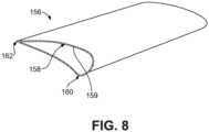
- Figure 8 illustrates a component 156 of an aircraft with a multilayer stack 158 deposited on or proximate to a surface 159 of the component 156, in accordance to an example implementation.
- the component 156 of the aircraft may, for example, represent a wing, a blade, or any other component of an aircraft.
- heat is generated for de-icing (i.e., melt any ice or snow accumulated about the component 156) or anti-icing (i.e., prevent ice from forming on the component 156).
- Distinct layers of the multilayer stacks 158 are not shown in Figure 8 to reduce visual clutter in the drawing. However, it should be understood that the multilayer stack 158 is similar to the multilayer stack of the device 129 shown in Figure 7 .
- the multilayer stack 158 could be deposited on the surface 159 of the component 156. In these examples, other protective layers could be deposited on top of the multilayer stack 158 for environmental protection and durability. In other examples, the multilayer stack 158 may be disposed within the component 156 proximate to the surface of the component 156, e.g., within a predetermined distance from the surface 159, so as to heat the surface of the component 156 and cause the ice to melt. In an example, the predetermined distance could range between 0.1 millimeter and 5 millimeter depending on thermal conductivity of the protective layers that separate the multilayer stack 158 from the surface of the component 156. By being proximate to the surface of the component 156, a lesser amount of heat can melt ice or prevent ice from forming, compared to a configuration where the multilayer stack 158 is disposed deeper within the component 156 away from its surface.
- the multilayer stack could also be used for shielding electronic components from electromagnetic interference (EMI).
- electronic components e.g., circuit boards
- the housing could be made of a plastic material configured to be the substrate (e.g., the substrate 100) of the multilayer stack.
- the method 164 includes repeating deposition of a respective insulating layer, and formation of a respective conductive polymer layer to form a multilayer stack of respective conductive polymer layers interposed between respective insulating layers (e.g., forming the conductive polymer layers 132, 144 interposed between the insulating layers 114, 136 and between the insulating layers 136, 148 to form the multilayer stack of the device 129 shown in Figure 7 ).
- Each respective conductive polymer layer has a respective electrical resistance, such that when the respective conductive polymer layers are connected in parallel to a power source (e.g., the power source 124), a resultant electrical resistance of the respective conductive polymer layers is less than each respective electrical resistance.
- the operations include forming the conductive polymer layer to include an intrinsic conductive polymer, or a mixture thereof with an extrinsic conductive polymer.
- the operation of depositing the insulating layer may include depositing a resin layer including polyurethane, epoxy, thermoplastic, phenolic, or silicone material. Further, the operation of forming the conductive polymer layer may include forming a layer of PANI-DNNSA, PEDOT-PSS, PANI-DBSA, or polypyrrole.
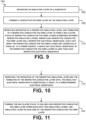
- FIG 10 is a flowchart of additional operations that may be executed and performed with the method 164, in accordance with an example implementation.
- operations include repeating the deposition of the respective insulating layer and the formation of the respective conductive layer until the resultant electrical resistance is substantially equal to a predetermined electrical resistance (e.g., within a percentage such as 1-3% of a target electrical resistance).
- FIG 11 is a flowchart of additional operations that may be executed and performed with the method 164, in accordance with an example implementation.
- operations include forming the multilayer stack to include each respective conductive polymer layer interfacing with two insulating layers, one insulating layer on each side of the respective conductive polymer layer (e.g., the conductive polymer layer 108 interfacing with the insulating layers 102, 114, the conductive polymer layer 132 interfacing with the insulating layers 114, 136, and the conductive polymer layer 144 interfacing with the insulating layers 136, 148).
- the conductive polymer layer 108 interfacing with the insulating layers 102, 114
- the conductive polymer layer 132 interfacing with the insulating layers 114, 136
- the conductive polymer layer 144 interfacing with the insulating layers 136, 148.
- FIG. 12 is a flowchart of additional operations that may be executed and performed with the method 164, in accordance with an example implementation.
- operations include treating the respective conductive polymer layers with a conductivity enhancer to enhance electrical conductivity of the respective conductive polymer layers.
- treating the respective conductive polymer layers with the conductivity enhancer comprises treating the respective conductive polymer layers with IPA.
- the respective conductive polymer layers may be treated with a band modifier to enhance electron hole mobility, and thus enhance electrical conductivity of the respective conductive polymer layers.
- FIG. 13 is a flowchart of additional operations that can be executed and performed with the method 164, in accordance with an example implementation.
- operations include forming a first electrical contact (e.g., first electrical contacts 118, 138, 150) on a first edge of each conductive polymer layer
- operations include forming a second electrical contact (e.g., second electrical contacts 120, 140, 152) on a second edge of each conductive polymer layer.
- the first electrical contacts and the second electrical contacts of the conductive polymer layers facilitate connecting the conductive polymer layers to the power source.
- FIG 14 is a flowchart of additional operations that can be executed and performed with the method 164, in accordance with an example implementation.
- operations include curing the insulating layer prior to forming the conductive polymer layer. Curing can be partial or can be full depending on the application and implementation.
- Figure 15 is a flowchart of additional operations that may be executed and performed with the method 164, in accordance with an example implementation.
- the operations of repeating deposition of a respective insulating layer, and formation of a respective conductive polymer layer to form a multilayer stack may include forming the multilayer stack to modify electrical resistivity over the substrate when the conductive polymer layers are connected in parallel to the power source.
- forming the multilayer stack to modify the electrical resistivity over the substrate may include depositing a different number of layers at different locations on the substrate.
- Forming the multilayer stack to modify the electrical resistivity over the substrate includes depositing conductive polymer layers having a different conductive polymer at different locations on the substrate.
- forming the multilayer stack to modify the electrical resistivity over the substrate may include depositing conductive polymer layers having different thicknesses at different locations on the substrate.
- conductive layers can selectively be treated with a conductivity enhancer while others might not be treated with a conductivity enhancer so as to vary electrical conductivity and resistivity across the substrate.
Landscapes
- Engineering & Computer Science (AREA)
- Microelectronics & Electronic Packaging (AREA)
- Physics & Mathematics (AREA)
- Spectroscopy & Molecular Physics (AREA)
- Manufacturing & Machinery (AREA)
- Chemical & Material Sciences (AREA)
- Electromagnetism (AREA)
- Dispersion Chemistry (AREA)
- General Chemical & Material Sciences (AREA)
- Chemical Kinetics & Catalysis (AREA)
- Laminated Bodies (AREA)
- Conductive Materials (AREA)
- Non-Insulated Conductors (AREA)
- Manufacturing Of Electric Cables (AREA)
- Application Of Or Painting With Fluid Materials (AREA)
- Secondary Cells (AREA)
- Parts Printed On Printed Circuit Boards (AREA)
Claims (15)
- Verfahren (164) zum Bilden eines Mehrschichtstapels (158) mit verbesserter Leitfähigkeit und Stabilität, wobei der Mehrschichtstapel (158) zum Enteisen einer Komponente eines Luftfahrzeugs, eines Drehflüglers oder einer Windturbine dient, wobei das Verfahren (164) aufweist:Aufbringen (166) einer Isolierschicht (102) auf ein Substrat (100);Bilden (168) einer leitenden Polymerschicht (108) auf der Isolierschicht (102); undWiederholen (170) eines Aufbringens einer jeweiligen Isolierschicht (114, 136), undBildung einer jeweiligen leitenden Polymerschicht (132), um den Mehrschichtstapel (158) aus jeweiligen leitenden Polymerschichten zu bilden, die zwischen jeweiligen Isolierschichten angeordnet sind, wobei jede jeweilige leitende Polymerschicht einen jeweiligen elektrischen Widerstand aufweist,wobei das Verfahren ferner ein paralleles elektrisches Verbinden der jeweiligen leitenden Polymerschichten aufweist, so dass ein resultierender elektrischer Widerstand der jeweiligen leitenden Polymerschichten kleiner als jeder jeweilige elektrische Widerstand ist,wobei ein Wiederholen (170) eines Aufbringens einer jeweiligen Isolierschicht und eine Bildung einer jeweiligen leitenden Polymerschicht zum Bilden eines Mehrschichtstapels ein Bilden (184) des Mehrschichtstapels (158) aufweist, um einen spezifischen elektrischen Widerstand über das Substrat (100) zu modifizieren, wenn die leitenden Polymerschichten (108, 132, 144) parallel mit einer Energiequelle (124) verbunden sind, wobei ein Bilden (184) des Mehrschichtstapels (158) zum Modifizieren des elektrischen Widerstands über dem Substrat (100) ein Aufbringen von leitenden Polymerschichten, die ein anders leitendes Polymer aufweisen, an unterschiedlichen Orten auf dem Substrat (100) aufweist, wobei ein Bilden (168) der leitenden Polymerschicht (108) ein Bilden der leitenden Polymerschicht (108) aufweist, um ein intrinsisch leitendes Polymer zu umfassen.
- Verfahren (164) nach Anspruch 1, wobei ein Wiederholen eines Aufbringens einer jeweiligen Isolierschicht und eine Bildung einer jeweiligen leitenden Polymerschicht zum Bilden eines Mehrschichtstapels ein Bilden (174) des Mehrschichtstapels (158) aufweist, um jeweils eine jeweilige leitende Polymerschicht (108, 132) zu umfassen, die mit zwei Isolierschichten (102, 114, 136) eine Schnittstelle mit einer Isolierschicht auf jeder Seite der jeweiligen leitenden Polymerschicht bildet.
- Verfahren (164) nach Anspruch 1 oder 2, das ferner aufweist:
Behandeln (176) der jeweiligen leitenden Polymerschichten mit einem Leitfähigkeitsverstärker, um die elektrische Leitfähigkeit der jeweiligen leitenden Polymerschichten zu stärken. - Verfahren (164) nach Anspruch 3, wobei ein Behandeln (176) der jeweiligen leitenden Polymerschichten mit dem Leitfähigkeitsverstärker ein Behandeln mit einem Morphologieverstärker oder mit einem Bandmodifikator aufweist.
- Verfahren (164) nach einem der Ansprüche 1-4, das ferner aufweist:Bilden (178) eines ersten elektrischen Kontakts (118) an einem ersten Rand jeder leitenden Polymerschicht; undBilden (180) eines zweiten elektrischen Kontakts (120) an einem zweiten Rand jeder leitenden Polymerschicht, wobei die ersten elektrischen Kontakte (118, 138, 150) und die zweiten elektrischen Kontakte (120, 140, 152) der leitenden Polymerschichten (108, 132, 144) ein Verbinden der leitenden Polymerschichten (108, 132, 144) mit einer Energiequelle (124) erleichtern.
- Verfahren (164) nach einem der Ansprüche 1-5, wobei ein Bilden (168) der leitenden Polymerschicht (108) ein Bilden der leitenden Polymerschicht (108) aufweist, um ein extrinsisch leitendes Polymer zu umfassen.
- Verfahren (164) nach einem der Ansprüche 1-6, wobei ein Aufbringen (166) der Isolierschicht ein Aufbringen (166) einer Harzschicht einschließlich Polyurethan, Epoxid-, Thermoplast-, Phenol- oder Silikonmaterial umfasst.
- Verfahren (164) nach einem der Ansprüche 1-7, wobei ein Bilden (168) der leitenden Polymerschicht ein Bilden (168) einer Schicht aus Polyanilin-Dinonylnaphthalinsulfonsäure (PANI-DNNSA), Poly(ethylendioxythiophen)-Poly(styrolsulfonat) (PEDOT-PSS), Polyanilin-Dodecylbenzolsulfonsäure (PANI-DBSA) oder Polypyrrol aufweist.
- Verfahren (164) nach einem der Ansprüche 1-8, das ferner aufweist:
Aushärten (182) der Isolierschicht (102) vor einem Bilden der leitenden Polymerschicht (108). - Verfahren (164) nach Anspruch 1, wobei ein Wiederholen der Aufbringung der jeweiligen Isolierschicht und der Bildung der jeweiligen leitenden Schicht aufweist: Wiederholen (172) der Aufbringung der jeweiligen Isolierschicht und Bildung der jeweiligen leitenden Schicht, bis der resultierende elektrische Widerstand im Wesentlichen gleich einem vorbestimmten elektrischen Widerstand ist.
- Verfahren (164) nach Anspruch 1, wobei die Isolierschicht (102) aus einem Harzmaterial gebildet wird.
- Verfahren (164) nach Anspruch 1, wobei die Isolierschicht (102) auf dem Substrat (100) durch Bürsten, Malen, Strukturieren, Drucken oder ein additives Herstellungsverfahren aufgebracht wird.
- Vorrichtung (129), die einen Mehrschichtstapel (158) mit einer verbesserten Leitfähigkeit und Stabilität aufweist, wobei der Mehrschichtstapel (158) zum Enteisen einer Komponente eines Luftfahrzeugs, eines Drehflüglers oder einer Windturbine dient, wobei die Vorrichtung (129) aufweist:ein Substrat (100); undden Mehrschichtstapel (158), der auf dem Substrat (100) aufgebracht ist, wobei der Mehrschichtstapel (158) eine Vielzahl von leitenden Polymerschichten (108, 132, 144) aufweist, wobei jede leitende Polymerschicht zwischen jeweiligen Isolierschichten (102, 114, 136, 148) angeordnet ist, wobei jede leitende Polymerschicht einen jeweiligen elektrischen Widerstand aufweist, wobei die Vielzahl von leitenden Polymerschichten parallel elektrisch verbunden sind und wobei eine Anzahl von leitenden Polymerschichten der Vielzahl von leitenden Polymerschichten derart ausgewählt ist, dass ein resultierender elektrischer Widerstand der leitenden Polymerschichten im Wesentlichen gleich einem vorbestimmten elektrischen Widerstand ist,wobei der Mehrschichtstapel (158) einen modifizierten spezifischen elektrischen Widerstand über das Substrat (100) aufweist, wenn die leitenden Polymerschichten (108, 132, 144) parallel mit einer Energiequelle (124) verbunden sind, wobei der modifizierte spezifische elektrische Widerstand über dem Substrat (100) leitende Polymerschichten, die ein anders leitendes Polymer aufweisen, an unterschiedlichen Orten auf dem Substrat (100) aufweist, wobei die leitende Polymerschicht (108) ein intrinsisch leitendes Polymer umfasst.
- Vorrichtung nach Anspruch 13, wobei das Substrat (100) aus einem Epoxidharz, einem Verbundstrukturmaterial, einem thermoplastischen Harz, einem wärmehärtenden Material oder einem Polycarbonatmaterial hergestellt ist.
- Vorrichtung nach Anspruch 13, wobei das Substrat (100) aus einem Verbundstrukturmaterial einer Komponente (156) eines Luftfahrzeugs hergestellt ist.
Applications Claiming Priority (1)
| Application Number | Priority Date | Filing Date | Title |
|---|---|---|---|
| US15/851,002 US10541065B2 (en) | 2017-12-21 | 2017-12-21 | Multilayer stack with enhanced conductivity and stability |
Publications (2)
| Publication Number | Publication Date |
|---|---|
| EP3506325A1 EP3506325A1 (de) | 2019-07-03 |
| EP3506325B1 true EP3506325B1 (de) | 2025-04-09 |
Family
ID=65009507
Family Applications (1)
| Application Number | Title | Priority Date | Filing Date |
|---|---|---|---|
| EP18212660.7A Active EP3506325B1 (de) | 2017-12-21 | 2018-12-14 | Mehrschichtiger stapel umfassend leitfähige polymerschichten mit verbesserter leitfähigkeit und stabilität und verfahren zur herstellung davon |
Country Status (5)
| Country | Link |
|---|---|
| US (2) | US10541065B2 (de) |
| EP (1) | EP3506325B1 (de) |
| JP (1) | JP7246177B2 (de) |
| CN (1) | CN110033911B (de) |
| CA (2) | CA3205331C (de) |
Families Citing this family (7)
| Publication number | Priority date | Publication date | Assignee | Title |
|---|---|---|---|---|
| US11702224B2 (en) | 2019-07-30 | 2023-07-18 | The Boeing Company | Lightning strike protection |
| US11952130B2 (en) | 2020-03-27 | 2024-04-09 | Airbus Operations Gmbh | Structural component for an aircraft with integrated heating layer and structural battery |
| CN111341223B (zh) * | 2020-04-09 | 2024-07-26 | 大连集思特科技有限公司 | 一种多层柔性透明显示电路、显示屏及其制作方法 |
| CN113571275B (zh) * | 2021-06-24 | 2022-03-11 | 贝迪斯电子有限公司 | 一种片式合金箔电阻的制造方法 |
| US11732145B2 (en) * | 2021-08-06 | 2023-08-22 | The Boeing Company | Conductive anti-icing coating systems and methods |
| CN116137777A (zh) * | 2021-11-16 | 2023-05-19 | 湖南亿润新材料科技有限公司 | 一种电磁屏蔽板及其制造方法 |
| WO2025201641A1 (en) * | 2024-03-27 | 2025-10-02 | Aeomiq Gmbh | Heating member for an ice protection system; parts equipped therewith and method for operating |
Family Cites Families (15)
| Publication number | Priority date | Publication date | Assignee | Title |
|---|---|---|---|---|
| US4942078A (en) | 1988-09-30 | 1990-07-17 | Rockwell International Corporation | Electrically heated structural composite and method of its manufacture |
| TW415624U (en) * | 1999-04-26 | 2000-12-11 | Polytronics Technology Corp | Surface mounted electric apparatus |
| CN1810068A (zh) | 2003-06-19 | 2006-07-26 | 波零公司 | 印刷电路板的emi吸收屏蔽 |
| US20050023974A1 (en) * | 2003-08-01 | 2005-02-03 | Universal Display Corporation | Protected organic electronic devices and methods for making the same |
| US7291815B2 (en) | 2006-02-24 | 2007-11-06 | Goodrich Corporation | Composite ice protection heater and method of producing same |
| TWI427646B (zh) * | 2006-04-14 | 2014-02-21 | Bourns Inc | 具表面可裝設配置之傳導聚合物電子裝置及其製造方法 |
| KR100915708B1 (ko) * | 2007-08-31 | 2009-09-04 | 한국기계연구원 | 도전성 박막과 전극을 구비한 발열기판 및 이의 제조방법 |
| FR2984418B1 (fr) | 2011-12-19 | 2014-01-24 | Valeol | Procede de degivrage de structures en materiaux composites, notamment de pales d'une eolienne, composition adaptee et dispositif adapte |
| US20140363637A1 (en) * | 2013-06-06 | 2014-12-11 | The Boeing Company | Heating Layer for Film Removal |
| JP6623513B2 (ja) | 2013-12-03 | 2019-12-25 | 東洋インキScホールディングス株式会社 | 電子素子およびシート材 |
| CA2961910C (en) * | 2014-09-22 | 2022-08-16 | Cytec Industries Inc. | Composite materials with high z-direction electrical conductivity |
| US20160196891A1 (en) * | 2014-09-26 | 2016-07-07 | The Boeing Company | Method for mitigating edge glow |
| EP3041058B1 (de) * | 2014-12-31 | 2019-09-11 | LG Display Co., Ltd. | Mehrschichtige umwandelbare vorrichtung und anzeigevorrichtung damit |
| JP2017103291A (ja) | 2015-11-30 | 2017-06-08 | 富士通株式会社 | 電磁波シールド構造体および電子機器 |
| CN110120288B (zh) * | 2018-02-07 | 2021-07-06 | 盛嘉伦热力科技(河源)有限公司 | Pptc电阻膜及应用该pptc电阻膜的电池 |
-
2017
- 2017-12-21 US US15/851,002 patent/US10541065B2/en active Active
-
2018
- 2018-12-13 CA CA3205331A patent/CA3205331C/en active Active
- 2018-12-13 CA CA3027652A patent/CA3027652C/en active Active
- 2018-12-14 EP EP18212660.7A patent/EP3506325B1/de active Active
- 2018-12-14 JP JP2018234351A patent/JP7246177B2/ja active Active
- 2018-12-21 CN CN201811570263.0A patent/CN110033911B/zh active Active
-
2019
- 2019-12-02 US US16/700,291 patent/US10607747B1/en active Active
Also Published As
| Publication number | Publication date |
|---|---|
| CA3027652C (en) | 2023-09-05 |
| US20200105436A1 (en) | 2020-04-02 |
| US10541065B2 (en) | 2020-01-21 |
| CA3027652A1 (en) | 2019-06-21 |
| CN110033911B (zh) | 2022-10-25 |
| US20190198188A1 (en) | 2019-06-27 |
| CN110033911A (zh) | 2019-07-19 |
| EP3506325A1 (de) | 2019-07-03 |
| CA3205331C (en) | 2025-08-05 |
| US10607747B1 (en) | 2020-03-31 |
| CA3205331A1 (en) | 2019-06-21 |
| JP2019116089A (ja) | 2019-07-18 |
| JP7246177B2 (ja) | 2023-03-27 |
Similar Documents
| Publication | Publication Date | Title |
|---|---|---|
| EP3506325B1 (de) | Mehrschichtiger stapel umfassend leitfähige polymerschichten mit verbesserter leitfähigkeit und stabilität und verfahren zur herstellung davon | |
| JP7214460B2 (ja) | 空力構造のための統合された雷保護および電気除氷 | |
| US20220183114A1 (en) | Multilayered panels | |
| JP6918633B2 (ja) | 航空機翼の加熱及び除氷用の導電性材料 | |
| Jillek et al. | Embedded components in printed circuit boards: a processing technology review | |
| CN104115580A (zh) | 雷击防护系统 | |
| WO2012092623A2 (en) | Anti-icing, de-icing, and heating configuration, integration, and power methods for aircraft, aerodynamic, and complex surfaces | |
| US10293956B2 (en) | Method for placing electrical conductors interior to a composite structure prior to curing | |
| US9855681B2 (en) | Ferrite compositions | |
| KR100987025B1 (ko) | 자기접착성을 갖는 도전성 시트 및 이의 제조방법 | |
| KR101311443B1 (ko) | 전자파 차폐 필름 및 그 제조방법 | |
| RU2192991C2 (ru) | Способ защиты топливных баков вертолета от термического воздействия тока молнии | |
| US12593402B2 (en) | Electronic device | |
| US7754975B2 (en) | Plastic component having heat resistant hardened resin at thermal-attachment connection points |
Legal Events
| Date | Code | Title | Description |
|---|---|---|---|
| PUAI | Public reference made under article 153(3) epc to a published international application that has entered the european phase |
Free format text: ORIGINAL CODE: 0009012 |
|
| STAA | Information on the status of an ep patent application or granted ep patent |
Free format text: STATUS: REQUEST FOR EXAMINATION WAS MADE |
|
| 17P | Request for examination filed |
Effective date: 20181214 |
|
| AK | Designated contracting states |
Kind code of ref document: A1 Designated state(s): AL AT BE BG CH CY CZ DE DK EE ES FI FR GB GR HR HU IE IS IT LI LT LU LV MC MK MT NL NO PL PT RO RS SE SI SK SM TR |
|
| AX | Request for extension of the european patent |
Extension state: BA ME |
|
| STAA | Information on the status of an ep patent application or granted ep patent |
Free format text: STATUS: EXAMINATION IS IN PROGRESS |
|
| 17Q | First examination report despatched |
Effective date: 20211013 |
|
| RAP3 | Party data changed (applicant data changed or rights of an application transferred) |
Owner name: THE BOEING COMPANY |
|
| GRAP | Despatch of communication of intention to grant a patent |
Free format text: ORIGINAL CODE: EPIDOSNIGR1 |
|
| STAA | Information on the status of an ep patent application or granted ep patent |
Free format text: STATUS: GRANT OF PATENT IS INTENDED |
|
| INTG | Intention to grant announced |
Effective date: 20241111 |
|
| P01 | Opt-out of the competence of the unified patent court (upc) registered |
Free format text: CASE NUMBER: APP_62768/2024 Effective date: 20241126 |
|
| GRAS | Grant fee paid |
Free format text: ORIGINAL CODE: EPIDOSNIGR3 |
|
| GRAA | (expected) grant |
Free format text: ORIGINAL CODE: 0009210 |
|
| STAA | Information on the status of an ep patent application or granted ep patent |
Free format text: STATUS: THE PATENT HAS BEEN GRANTED |
|
| AK | Designated contracting states |
Kind code of ref document: B1 Designated state(s): AL AT BE BG CH CY CZ DE DK EE ES FI FR GB GR HR HU IE IS IT LI LT LU LV MC MK MT NL NO PL PT RO RS SE SI SK SM TR |
|
| REG | Reference to a national code |
Ref country code: GB Ref legal event code: FG4D |
|
| REG | Reference to a national code |
Ref country code: CH Ref legal event code: EP |
|
| REG | Reference to a national code |
Ref country code: DE Ref legal event code: R096 Ref document number: 602018080908 Country of ref document: DE |
|
| REG | Reference to a national code |
Ref country code: IE Ref legal event code: FG4D |
|
| REG | Reference to a national code |
Ref country code: NL Ref legal event code: MP Effective date: 20250409 |
|
| PG25 | Lapsed in a contracting state [announced via postgrant information from national office to epo] |
Ref country code: NL Free format text: LAPSE BECAUSE OF FAILURE TO SUBMIT A TRANSLATION OF THE DESCRIPTION OR TO PAY THE FEE WITHIN THE PRESCRIBED TIME-LIMIT Effective date: 20250409 |
|
| REG | Reference to a national code |
Ref country code: AT Ref legal event code: MK05 Ref document number: 1784334 Country of ref document: AT Kind code of ref document: T Effective date: 20250409 |
|
| PG25 | Lapsed in a contracting state [announced via postgrant information from national office to epo] |
Ref country code: ES Free format text: LAPSE BECAUSE OF FAILURE TO SUBMIT A TRANSLATION OF THE DESCRIPTION OR TO PAY THE FEE WITHIN THE PRESCRIBED TIME-LIMIT Effective date: 20250409 Ref country code: PT Free format text: LAPSE BECAUSE OF FAILURE TO SUBMIT A TRANSLATION OF THE DESCRIPTION OR TO PAY THE FEE WITHIN THE PRESCRIBED TIME-LIMIT Effective date: 20250811 Ref country code: FI Free format text: LAPSE BECAUSE OF FAILURE TO SUBMIT A TRANSLATION OF THE DESCRIPTION OR TO PAY THE FEE WITHIN THE PRESCRIBED TIME-LIMIT Effective date: 20250409 |
|
| REG | Reference to a national code |
Ref country code: LT Ref legal event code: MG9D |
|
| PG25 | Lapsed in a contracting state [announced via postgrant information from national office to epo] |
Ref country code: GR Free format text: LAPSE BECAUSE OF FAILURE TO SUBMIT A TRANSLATION OF THE DESCRIPTION OR TO PAY THE FEE WITHIN THE PRESCRIBED TIME-LIMIT Effective date: 20250710 Ref country code: NO Free format text: LAPSE BECAUSE OF FAILURE TO SUBMIT A TRANSLATION OF THE DESCRIPTION OR TO PAY THE FEE WITHIN THE PRESCRIBED TIME-LIMIT Effective date: 20250709 |
|
| PG25 | Lapsed in a contracting state [announced via postgrant information from national office to epo] |
Ref country code: PL Free format text: LAPSE BECAUSE OF FAILURE TO SUBMIT A TRANSLATION OF THE DESCRIPTION OR TO PAY THE FEE WITHIN THE PRESCRIBED TIME-LIMIT Effective date: 20250409 |
|
| PG25 | Lapsed in a contracting state [announced via postgrant information from national office to epo] |
Ref country code: BG Free format text: LAPSE BECAUSE OF FAILURE TO SUBMIT A TRANSLATION OF THE DESCRIPTION OR TO PAY THE FEE WITHIN THE PRESCRIBED TIME-LIMIT Effective date: 20250409 |
|
| PG25 | Lapsed in a contracting state [announced via postgrant information from national office to epo] |
Ref country code: HR Free format text: LAPSE BECAUSE OF FAILURE TO SUBMIT A TRANSLATION OF THE DESCRIPTION OR TO PAY THE FEE WITHIN THE PRESCRIBED TIME-LIMIT Effective date: 20250409 |
|
| PG25 | Lapsed in a contracting state [announced via postgrant information from national office to epo] |
Ref country code: AT Free format text: LAPSE BECAUSE OF FAILURE TO SUBMIT A TRANSLATION OF THE DESCRIPTION OR TO PAY THE FEE WITHIN THE PRESCRIBED TIME-LIMIT Effective date: 20250409 |
|
| PG25 | Lapsed in a contracting state [announced via postgrant information from national office to epo] |
Ref country code: RS Free format text: LAPSE BECAUSE OF FAILURE TO SUBMIT A TRANSLATION OF THE DESCRIPTION OR TO PAY THE FEE WITHIN THE PRESCRIBED TIME-LIMIT Effective date: 20250709 |
|
| PG25 | Lapsed in a contracting state [announced via postgrant information from national office to epo] |
Ref country code: IS Free format text: LAPSE BECAUSE OF FAILURE TO SUBMIT A TRANSLATION OF THE DESCRIPTION OR TO PAY THE FEE WITHIN THE PRESCRIBED TIME-LIMIT Effective date: 20250809 |
|
| PG25 | Lapsed in a contracting state [announced via postgrant information from national office to epo] |
Ref country code: LV Free format text: LAPSE BECAUSE OF FAILURE TO SUBMIT A TRANSLATION OF THE DESCRIPTION OR TO PAY THE FEE WITHIN THE PRESCRIBED TIME-LIMIT Effective date: 20250409 |
|
| PGFP | Annual fee paid to national office [announced via postgrant information from national office to epo] |
Ref country code: GB Payment date: 20251229 Year of fee payment: 8 |
|
| REG | Reference to a national code |
Ref country code: DE Ref legal event code: R097 Ref document number: 602018080908 Country of ref document: DE |
|
| PG25 | Lapsed in a contracting state [announced via postgrant information from national office to epo] |
Ref country code: DK Free format text: LAPSE BECAUSE OF FAILURE TO SUBMIT A TRANSLATION OF THE DESCRIPTION OR TO PAY THE FEE WITHIN THE PRESCRIBED TIME-LIMIT Effective date: 20250409 Ref country code: SM Free format text: LAPSE BECAUSE OF FAILURE TO SUBMIT A TRANSLATION OF THE DESCRIPTION OR TO PAY THE FEE WITHIN THE PRESCRIBED TIME-LIMIT Effective date: 20250409 |
|
| PGFP | Annual fee paid to national office [announced via postgrant information from national office to epo] |
Ref country code: FR Payment date: 20251226 Year of fee payment: 8 |
|
| PG25 | Lapsed in a contracting state [announced via postgrant information from national office to epo] |
Ref country code: CZ Free format text: LAPSE BECAUSE OF FAILURE TO SUBMIT A TRANSLATION OF THE DESCRIPTION OR TO PAY THE FEE WITHIN THE PRESCRIBED TIME-LIMIT Effective date: 20250409 |
|
| PG25 | Lapsed in a contracting state [announced via postgrant information from national office to epo] |
Ref country code: EE Free format text: LAPSE BECAUSE OF FAILURE TO SUBMIT A TRANSLATION OF THE DESCRIPTION OR TO PAY THE FEE WITHIN THE PRESCRIBED TIME-LIMIT Effective date: 20250409 |
|
| PG25 | Lapsed in a contracting state [announced via postgrant information from national office to epo] |
Ref country code: SK Free format text: LAPSE BECAUSE OF FAILURE TO SUBMIT A TRANSLATION OF THE DESCRIPTION OR TO PAY THE FEE WITHIN THE PRESCRIBED TIME-LIMIT Effective date: 20250409 Ref country code: RO Free format text: LAPSE BECAUSE OF FAILURE TO SUBMIT A TRANSLATION OF THE DESCRIPTION OR TO PAY THE FEE WITHIN THE PRESCRIBED TIME-LIMIT Effective date: 20250409 |
|
| PG25 | Lapsed in a contracting state [announced via postgrant information from national office to epo] |
Ref country code: IT Free format text: LAPSE BECAUSE OF FAILURE TO SUBMIT A TRANSLATION OF THE DESCRIPTION OR TO PAY THE FEE WITHIN THE PRESCRIBED TIME-LIMIT Effective date: 20250409 |
|
| PLBE | No opposition filed within time limit |
Free format text: ORIGINAL CODE: 0009261 |
|
| STAA | Information on the status of an ep patent application or granted ep patent |
Free format text: STATUS: NO OPPOSITION FILED WITHIN TIME LIMIT |
|
| REG | Reference to a national code |
Ref country code: CH Ref legal event code: L10 Free format text: ST27 STATUS EVENT CODE: U-0-0-L10-L00 (AS PROVIDED BY THE NATIONAL OFFICE) Effective date: 20260218 |
|
| 26N | No opposition filed |
Effective date: 20260112 |
|
| PGFP | Annual fee paid to national office [announced via postgrant information from national office to epo] |
Ref country code: DE Payment date: 20251229 Year of fee payment: 8 |