EP3506249A1 - Display device and display method - Google Patents
Display device and display method Download PDFInfo
- Publication number
- EP3506249A1 EP3506249A1 EP19158011.7A EP19158011A EP3506249A1 EP 3506249 A1 EP3506249 A1 EP 3506249A1 EP 19158011 A EP19158011 A EP 19158011A EP 3506249 A1 EP3506249 A1 EP 3506249A1
- Authority
- EP
- European Patent Office
- Prior art keywords
- display
- peak level
- partial
- video signal
- display device
- Prior art date
- Legal status (The legal status is an assumption and is not a legal conclusion. Google has not performed a legal analysis and makes no representation as to the accuracy of the status listed.)
- Withdrawn
Links
Images


Classifications
-
- G—PHYSICS
- G09—EDUCATION; CRYPTOGRAPHY; DISPLAY; ADVERTISING; SEALS
- G09G—ARRANGEMENTS OR CIRCUITS FOR CONTROL OF INDICATING DEVICES USING STATIC MEANS TO PRESENT VARIABLE INFORMATION
- G09G3/00—Control arrangements or circuits, of interest only in connection with visual indicators other than cathode-ray tubes
- G09G3/20—Control arrangements or circuits, of interest only in connection with visual indicators other than cathode-ray tubes for presentation of an assembly of a number of characters, e.g. a page, by composing the assembly by combination of individual elements arranged in a matrix no fixed position being assigned to or needed to be assigned to the individual characters or partial characters
- G09G3/34—Control arrangements or circuits, of interest only in connection with visual indicators other than cathode-ray tubes for presentation of an assembly of a number of characters, e.g. a page, by composing the assembly by combination of individual elements arranged in a matrix no fixed position being assigned to or needed to be assigned to the individual characters or partial characters by control of light from an independent source
- G09G3/3406—Control of illumination source
- G09G3/342—Control of illumination source using several illumination sources separately controlled corresponding to different display panel areas, e.g. along one dimension such as lines
- G09G3/3426—Control of illumination source using several illumination sources separately controlled corresponding to different display panel areas, e.g. along one dimension such as lines the different display panel areas being distributed in two dimensions, e.g. matrix
-
- G—PHYSICS
- G09—EDUCATION; CRYPTOGRAPHY; DISPLAY; ADVERTISING; SEALS
- G09G—ARRANGEMENTS OR CIRCUITS FOR CONTROL OF INDICATING DEVICES USING STATIC MEANS TO PRESENT VARIABLE INFORMATION
- G09G3/00—Control arrangements or circuits, of interest only in connection with visual indicators other than cathode-ray tubes
- G09G3/20—Control arrangements or circuits, of interest only in connection with visual indicators other than cathode-ray tubes for presentation of an assembly of a number of characters, e.g. a page, by composing the assembly by combination of individual elements arranged in a matrix no fixed position being assigned to or needed to be assigned to the individual characters or partial characters
- G09G3/34—Control arrangements or circuits, of interest only in connection with visual indicators other than cathode-ray tubes for presentation of an assembly of a number of characters, e.g. a page, by composing the assembly by combination of individual elements arranged in a matrix no fixed position being assigned to or needed to be assigned to the individual characters or partial characters by control of light from an independent source
- G09G3/36—Control arrangements or circuits, of interest only in connection with visual indicators other than cathode-ray tubes for presentation of an assembly of a number of characters, e.g. a page, by composing the assembly by combination of individual elements arranged in a matrix no fixed position being assigned to or needed to be assigned to the individual characters or partial characters by control of light from an independent source using liquid crystals
-
- G—PHYSICS
- G09—EDUCATION; CRYPTOGRAPHY; DISPLAY; ADVERTISING; SEALS
- G09G—ARRANGEMENTS OR CIRCUITS FOR CONTROL OF INDICATING DEVICES USING STATIC MEANS TO PRESENT VARIABLE INFORMATION
- G09G2320/00—Control of display operating conditions
- G09G2320/02—Improving the quality of display appearance
- G09G2320/0271—Adjustment of the gradation levels within the range of the gradation scale, e.g. by redistribution or clipping
-
- G—PHYSICS
- G09—EDUCATION; CRYPTOGRAPHY; DISPLAY; ADVERTISING; SEALS
- G09G—ARRANGEMENTS OR CIRCUITS FOR CONTROL OF INDICATING DEVICES USING STATIC MEANS TO PRESENT VARIABLE INFORMATION
- G09G2320/00—Control of display operating conditions
- G09G2320/02—Improving the quality of display appearance
- G09G2320/0285—Improving the quality of display appearance using tables for spatial correction of display data
-
- G—PHYSICS
- G09—EDUCATION; CRYPTOGRAPHY; DISPLAY; ADVERTISING; SEALS
- G09G—ARRANGEMENTS OR CIRCUITS FOR CONTROL OF INDICATING DEVICES USING STATIC MEANS TO PRESENT VARIABLE INFORMATION
- G09G2320/00—Control of display operating conditions
- G09G2320/06—Adjustment of display parameters
- G09G2320/0613—The adjustment depending on the type of the information to be displayed
- G09G2320/062—Adjustment of illumination source parameters
-
- G—PHYSICS
- G09—EDUCATION; CRYPTOGRAPHY; DISPLAY; ADVERTISING; SEALS
- G09G—ARRANGEMENTS OR CIRCUITS FOR CONTROL OF INDICATING DEVICES USING STATIC MEANS TO PRESENT VARIABLE INFORMATION
- G09G2320/00—Control of display operating conditions
- G09G2320/06—Adjustment of display parameters
- G09G2320/0626—Adjustment of display parameters for control of overall brightness
- G09G2320/0646—Modulation of illumination source brightness and image signal correlated to each other
Definitions
- the present disclosure relates to a display device having liquid crystal display elements and to a display method thereof.
- CRTs Cathode Ray Tubes
- liquid crystal display devices are on their way to going mainstream for low power consumption.
- Japanese Patent Laid-Open No. 2009-42652 and Japanese Patent Laid-Open No. 2010-113099 disclose display devices that are designed to independently control the emission luminance of the backlight (partially drive the backlight) in each of a plurality of areas into which the backlight is divided according to luminance information of a video signal.
- a display device includes a liquid crystal display section, backlight and processing section.
- the liquid crystal display section displays an image based on a video signal.
- the processing section corrects the video signal and sets the luminance of the backlight based on two pieces of information, a peak level of the video signal in a display screen or in each of a plurality of partial display areas into which the display screen is divided, and factor data obtained from a data map made up of a reference position on the display screen and the factor data that are associated with each other.
- a display device includes a liquid crystal display section, backlight and processing section.
- the liquid crystal display section displays an image based on a video signal.
- the processing section corrects the video signal and sets the luminance of the backlight based on two pieces of information, a peak level of the video signal in a display screen or in each of a plurality of partial display areas into which the display screen is divided, and a peak position, i.e., a position on the display screen where the peak level occurs.
- a display device includes a liquid crystal display section, backlight and processing section.
- the liquid crystal display section displays an image based on a video signal.
- the backlight has a plurality of partial light-emitting sections.
- the processing section corrects the video signal and sets the luminance of each of the partial light-emitting sections based on two pieces of information, a peak level of the video signal in a partial display area associated with one of the partial light-emitting sections, and the position of that partial display area.
- a display method corrects a video signal and sets the luminance of a backlight based on two pieces of information, a peak level of the video signal in a display screen or in each of a plurality of partial display areas into which the display screen is divided, and factor data obtained from a data map made up of a position on the display screen and the factor data that are associated with each other so as to display an image based on the corrected video signal.
- the liquid crystal display section displays an image based on the video signal.
- the video signal is corrected, and the luminance of the backlight is set, based on the peak level and the factor data obtained from the data map.
- An image is displayed based on the corrected video signal.
- the liquid crystal display section displays an image based on the video signal.
- the video signal is corrected, and the luminance of the backlight is set, based on the peak level and peak position.
- An image is displayed based on the corrected video signal.
- the liquid crystal display section displays an image based on the video signal.
- the video signal is corrected, and the luminance of the partial light-emitting section associated with the partial display area is set, based on the peak level and the position of the partial display area.
- An image is displayed based on the corrected video signal.
- the display device correct the video signal and set the luminance of the backlight based on the peak level and the factor data obtained from the data map, thus providing reduced power consumption.
- the display device corrects the video signal and sets the luminance of the backlight based on the peak level and peak position, thus providing reduced power consumption.
- the display device corrects the video signal and sets the luminance of the partial light-emitting section based on the peak level and the position of the partial display area, thus providing reduced power consumption.
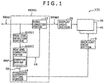
- FIG. 1 illustrates a configuration example of a display device according to a first embodiment.
- a display device 1 is a transmissive liquid crystal display device having a backlight. It should be noted that the display method according to the embodiments of the present disclosure is implemented by the present embodiment. Therefore, the display method will be described together with the first embodiment.
- the display device 1 includes a signal processing section 10, display drive section 20, liquid crystal display section 30, backlight drive section 9 and backlight 40.
- the signal processing section 10 generates a video signal Sdisp2 and sets the luminance of the backlight 40 based on a video signal Sdisp.
- the signal processing section 10 will be described in detail later.
- the display drive section 20 drives the liquid crystal display section 30 based on the video signal Sdisp2 supplied from the signal processing section 10.
- the liquid crystal display section 30 includes liquid crystal display elements and displays an image by modulating light emitted from the backlight 40.
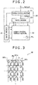
- Fig. 2 illustrates an example of a block diagram of the display drive section 20 and liquid crystal display section 30.
- the display drive section 20 includes a timing control portion 21, gate driver 22 and data driver 23.
- the timing control portion 21 controls the drive timings of the gate driver 22 and data driver 23, and supplies the video signal Sdisp2, supplied from a control section 24, to the data driver 23 as a video signal Sdisp3.
- the gate driver 22 selects pixels Pix in the liquid crystal display section 30 one row at a time in sequence under timing control of the timing control portion 21, thus progressively scanning the pixels Pix.
- the data driver 23 supplies a pixel signal based on the video signal Sdisp3 to each of the pixels Pix of the liquid crystal display section 30. More specifically, the data driver 23 handles digital-to-analog conversion based on the video signal Sdisp3, thus generating a pixel signal, i.e., an analog signal, and supplying the pixel signal to each of the pixels Pix.
- the liquid crystal display section 30 has a liquid crystal material sealed between two transparent substrates that are made, for example, of glass.
- Transparent electrodes made, for example, of ITO (Indium Tin Oxide) are formed in the areas of these transparent substrates facing the liquid crystal material, thus making up the pixels Pix together with the liquid crystal material.
- ITO Indium Tin Oxide
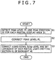
- Fig. 3 illustrates an example of a circuit diagram of the liquid crystal display section 30.
- the liquid crystal display section 30 includes the plurality of pixels Pix that are arranged in a matrix form.
- Each of the pixels Pix includes three (red, green and blue) subpixels SPix.
- Each of the subpixels SPix has a TFT (thin-film transistor) element Tr and liquid crystal element LC.
- the TFT element Tr includes a thin film transistor.
- the TFT element Tr includes an n-channel MOS (Metal Oxide Semiconductor) TFT.
- the TFT element Tr has its source connected to a data line SGL, its gate connected to a gate line GCL and its drain connected to one end of the liquid crystal element LC.
- the liquid crystal element LC has one of its ends connected to the drain of the TFT element Tr and the other end grounded.
- the gate line GCL is connected to the gate driver 22, and the data line SGL to the data driver 23.
- the backlight 40 emits light based on a drive signal supplied from the backlight drive section 9 and directs it to the liquid crystal display section 30.
- Fig. 4 illustrates a configuration example of the backlight 40.
- the backlight 40 is a so-called direct backlight having a plurality of partial light-emitting sections 41 arranged in a matrix form.
- Each of the partial light-emitting sections 41 includes an LED (Light Emitting Diode) in this example.
- the lamp making up the partial light-emitting section 41 is not limited to an LED.
- a CCFL Cold Cathode Fluorescent Lamp
- the partial light-emitting sections 41 can each emit light independently of each other at the set luminance. Light emitted from each of the partial light-emitting sections 41 passes through the associated area (partial display area 31 which will be described later) of the liquid crystal display section 30 and is emitted from the display device 1.
- the signal processing section 10 includes a peak level detection portion 11, peak level correction portion 12, signal correction portion 13 and luminance setting portion 14.
- the peak level detection portion 11 detects a peak level PL representing the highest luminance of all the levels of the video signal Sdisp for each of the subpixels SPix.
- Fig. 5 schematically illustrates a display screen S of the display device 1.
- the display screen S is divided into the partial display areas 31 that are arranged in a matrix form.
- Each of the partial display areas 31 is associated with one of the partial light-emitting sections 41 of the backlight 40. That is, light emitted from each of the partial light-emitting sections 41 passes through the associated partial display area 31.
- each of the partial display areas 31 is divided into a plurality of unit areas 32 (two unit areas 32 in this case).
- the peak level detection portion 11 detects the peak level PL of the video signal Sdisp for each of the partial display areas 31.
- the peak level PL is normalized so that the minimum signal level is "0," and the maximum signal level is "1.”
- minimum signal level refers to the level of the video signal Sdisp that provides the minimum luminous transmittance (so-called black level) of the liquid crystal element LC
- maximum signal level to the level of the video signal Sdisp that provides the maximum luminous transmittance (so-called white level) of the liquid crystal element LC.
- the peak level detection portion 11 supplies, to the peak level correction portion 12, the position of the unit area 32, i.e., one of the two unit areas 32 belonging to that partial display area 31, where the peak level PL has been detected, together with the detected peak level PL for each of the partial display areas 31.
- the peak level correction portion 12 corrects the peak level PL based on the peak level PL and a peak position PP supplied from the peak level detection portion 11, thus generating a peak level PL2.
- the peak level correction portion 12 has a correction data map MAP as illustrated in Fig. 1 and corrects the peak level PL using the correction data map MAP.
- Fig. 6 illustrates an example of the correction data map MAP.
- the correction data map MAP represents a map of correction data DT in the display screen S.
- the correction data DT is set for each of the unit areas 32.
- the areas RA to RC have different values as the correction data DT.
- the area RA is provided at and near the center of the display screen S.
- the area RB is provided to surround the area RA.
- the area RC is provided on the outside of the area RB.
- the correction data DT is set to "1.0" in the area RA, to "0.9” in the area RB, and to "0.8" in the area RC.
- the peak level correction portion 12 corrects the peak level PL using the correction data map MAP based on the peak level PL and peak position PP for each of the partial display areas 31 supplied from the peak level detection portion 11. More specifically, the peak level correction portion 12 acquires the correction data DT in the unit area 32 indicated by the peak position PP using the correction data map MAP first as will be described later. Then, the peak level correction portion 12 multiplies the correction data DT by the peak level PL in the partial display area 31 including that unit area 32, thus correcting the peak level PL and generating the peak level PL2. Then, the peak level correction portion 12 finds a gain factor G1 using a function F1 based on the peak level PL2, thus supplying the gain factor G1 to the signal correction portion 13.
- the function F1 increases the gain factor G1 as the peak level PL2 decreases.
- the peak level correction portion 12 finds a luminance factor G2 using a function F2 based on the peak level PL2.
- the function F2 increases the luminance factor G2 as the peak level PL2 increases.
- a LUT Look Up Table
- the signal correction portion 13 corrects the level of the video signal Sdisp for each of the partial display areas 31 based on the gain factor G1 of the partial display areas 31, thus outputting it as the video signal Sdisp2. More specifically, the signal correction portion 13 multiplies the level of the video signal Sdisp by the gain factor G1 for each of the partial display areas 31, thus correcting the level of the video signal Sdisp as will be described later.
- the luminance setting portion 14 sets the luminance of each of the partial light-emitting sections 41 of the backlight 40 based on the luminance factor G2 of each of the partial display areas 31. More specifically, the luminance setting portion 14 sets the partial light-emitting section 41 associated with the partial display area 31 to a luminance proportional to the luminance factor G2 as will be described later.
- the correction data map MAP corresponds to a specific example of a "data map” in the present disclosure
- the correction data DT to a specific example of "factor data.”
- the signal processing section 10 corresponds to a specific example of a “processing section” in the present disclosure.
- the areas RA to RC correspond to specific examples of "factor data areas” in the present disclosure, and the area RA to a specific example of a "specific factor data area.”
- the signal processing section 10 generates the video signal Sdisp2 and sets the luminance of each of the partial light-emitting sections 41 of the backlight 40 based on the video signal Sdisp. More specifically, the peak level detection portion 11 detects the peak level PL and peak position PP of the video signal Sdisp for each of the partial display areas 31.
- the peak level correction portion 12 generates the peak level PL2 by correcting the peak level PL using the correction data map MAP based on the peak level PL and peak position PP, thus finding the gain factor G1 and luminance factor G2 based on the peak level PL2.
- the signal correction portion 13 corrects the video signal Sdisp for each of the partial display areas 31 based on the gain factor G1, thus generating the video signal Sdisp2.
- the luminance setting portion 14 sets the luminance of each of the partial light-emitting sections 41 of the backlight 40 based on the luminance factor G2.
- the display drive section 20 drives the liquid crystal display section 30.
- the liquid crystal display section 30 displays an image by modulating light emitted from the backlight 40.
- the backlight drive section 9 drives the backlight 40.
- Each of the partial light-emitting sections 41 of the backlight 40 emits light based on a drive signal supplied from the backlight drive section 9 and directs it to the liquid crystal display section 30.
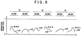
- Fig. 7 illustrates an operation example of the signal processing section 10.
- the signal processing section 10 detects the peak level PL of the supplied video signal Sdisp for each of the partial display areas 31 first, and then generates the peak level PL2 by correcting the peak level PL using the correction data map MAP, thus finding the gain factor G1 and luminance factor G2 based on the peak level PL2. Then, the signal processing section 10 corrects the video signal Sdisp based on the gain factor G1 and sets the luminance of the partial light-emitting section 41 associated with that partial display area 31 based on the luminance factor G2. A detailed description thereof will be given below.
- the peak level detection portion 11 of the signal processing section 10 detects the peak level PL and peak position PP of the video signal Sdisp for each of the partial display areas 31 (step S1).
- Fig. 8 schematically illustrates examples of normalized signal levels LA1 to LA6 of the video signal Sdisp in unit areas A1 to A6 shown in Fig. 5 .
- the horizontal axis represents all the subpixels SPix respectively belonging to the unit areas A1 to A6. That is, the curves having the signal levels LA1 to LA6 represent the signal levels of all the subpixels SPix belonging to the unit areas A1 to A6, respectively.
- the maximum value of the signal levels LA1 and LA2 is, for example, 0.5 (peak level PL) in the partial display area 31 that includes the unit areas A1 and A2.
- the unit area 32 having this maximum value is the unit area A1 (peak position PP).
- the maximum value of the signal levels LA3 and LA4 is, for example, 0.5 (peak level PL) in the partial display area 31 that includes the unit areas A3 and A4.
- the unit area 32 having this maximum value is the unit area A4 (peak position PP).
- the maximum value of the signal levels LA5 and LA6 is, for example, 0.5 (peak level PL) in the partial display area 31 that includes the unit areas A5 and A6.
- the unit area 32 having this maximum value is the unit area A6 (peak position PP).
- the peak level detection portion 11 detects the peak level PL and peak position PP in all the partial display areas 31 as described above. It should be noted that the peak levels PL are all 0.5 as shown above for reasons of convenience in this example. However, the present disclosure is not limited thereto. Instead, the peak levels may take on any value between 0 and 1.
- the peak level correction portion 12 of the signal processing section 10 corrects the peak level PL detected by the peak level detection portion 11 (step S2). More specifically, the peak level correction portion 12 acquires the correction data DT in the unit area 32 indicated by the peak position PP using the correction data map MAP first. Then, the peak level correction portion 12 multiplies the correction data DT by the peak level PL in the partial display area 31, thus correcting the peak level PL and generating the peak level PL2.
- the peak level correction portion 12 corrects the peak level PL in all the partial display areas 31 as described above, thus generating the peak level PL2.
- the signal processing section 10 corrects the level of the video signal Sdisp and sets the luminance of each of the partial light-emitting sections 41 of the backlight 40 (step S3).
- Figs. 9A and 9B illustrate an example of the process performed in step S3 if the signal levels are as shown in Fig. 8 .
- Fig. 9A illustrates the correction of the level of the video signal Sdisp
- Fig. 9B the setting of the luminance of the partial light-emitting sections 41.
- the peak level correction portion 12 of the signal processing section 10 finds the gain factor G1 using the function F1 based on the peak level PL2 and also finds the luminance factor G2 using the function F2 for each of the partial display areas 31. Then, the signal correction portion 13 of the signal processing section 10 multiplies the level of the video signal Sdisp by the gain factor G1 for each of the partial display areas 31 as illustrated in Fig. 9A , thus correcting the level of the video signal Sdisp. Further, the luminance setting portion 14 of the signal processing section 10 sets the partial light-emitting sections 41, each associated with one of the partial display areas 31, to a luminance proportional to the luminance factor G2 as illustrated in Fig. 9B .
- the signal correction portion 13 multiplies the level of the video signal Sdisp by the gain factor G1 associated with the peak level PL2 (0.5) ( Fig. 9A ). Further, the luminance setting portion 14 sets the associated partial light-emitting section 41 to a luminance proportional to the luminance factor G2 associated with the peak level PL2 (0.5) ( Fig. 9B ).
- the signal correction portion 13 multiplies the level of the video signal Sdisp by the gain factor G1 associated with the peak level PL2 (0.45) ( Fig. 9A ). Further, the luminance setting portion 14 sets the associated partial fight-emitting section 41 to a luminance proportional to the luminance factor G2 associated with the peak level PL2 (0.45) ( Fig. 9B ).
- the peak level PL2 (0.45) in the unit areas A3 and A4 is smaller than that (0.5) in the unit areas A1 and A2. Therefore, the gain factor G1 in the unit areas A3 and A4 is greater than that in the unit areas A1 and A2, and the luminance factor G2 in the unit areas A3 and A4 is smaller than that in the unit areas A1 and A2.
- the signal correction portion 13 multiplies the level of the video signal Sdisp by the gain factor G1 associated with the peak level PL2 (0.4) ( Fig. 9A ).
- the luminance setting portion 14 sets the associated partial light-emitting section 41 to a luminance proportional to the luminance factor G2 associated with the peak level PL2 (0.4) ( Fig. 9B ).
- the peak level PL2 (0.4) in the unit areas A5 and A6 is smaller than that (0.45) in the unit areas A3 and A4. Therefore, the gain factor G1 in the unit areas A5 and A6 is greater than that in the unit areas A3 and A4, and the luminance factor G2 in the unit areas A5 and A6 is smaller than that in the unit areas A3 and A4.
- the signal processing section 10 corrects the level of the video signal Sdisp in all the partial display areas 31 and sets the luminance of each of all the partial light-emitting sections 41 as described above.
- the signal processing section 10 processes each frame image supplied via the video signal Sdisp as described above.
- the luminance of the associated partial light-emitting section 41 is set according to the level of the video signal Sdisp for each of the partial display areas 31 in the display device 1.
- the lower the level of the video signal Sdisp (peak level PL) the more the luminance of the partial light-emitting section 41 can be reduced, thus contributing to reduced power consumption of the backlight 40.
- the correction data map MAP has the three areas RA to RC provided therein that differ in the correction data DT from each other.
- the correction data DT is 1.0. Therefore, the luminance of the associated partial light-emitting section 41 can be reduced without degrading the image quality. That is, in the partial display area 31 that includes the unit areas A1 and A2 (on the left in Figs. 8 , 9A and 9B ), for example, the signal levels are multiplied by the gain factor G1 for correction, and the luminance of the partial light-emitting sections 41 is set to be proportional to the luminance factor G2. At this time, the corrected signal levels do not exceed the so-called white level ( Fig. 9A ). This prevents or at least reduces the degradation of the image quality, thus contributing to reduced power consumption without degrading the image quality.
- the correction data DT is 0.9. Therefore, the luminance of the associated partial light-emitting section 41 can be further reduced although the image quality declines to a small extent. That is, in this partial display area 31, the corrected signal level for some of the subpixels SPix exceeds the white level and is saturated (portion W1 in Fig. 9A ). In this case, the luminance of the subpixel SPix is lower than the desired one and not sufficient. Further, if, for example, the signal level of only the subpixel SPix of a certain color is saturated, a so-called color shift occurs. If the corrected signal level is saturated as described above, the image quality may degrade due to insufficient luminance or color shift.
- the area RB is provided to surround the area RA that is provided at and near the center of the display screen S ( Fig. 6 ). Therefore, it is unlikely that the area RB will attract more attention of the viewer than the area RA. Therefore, even if a color shift or other problem occurs in the partial display areas 31 of the area RB, it is unlikely that the viewer will perceive the degradation of image quality.
- the luminance of the partial light-emitting sections 41 of the area RB can be reduced more than that of the partial light-emitting sections 41 of the area RA ( Fig. 9B ), thus contributing to reduced power consumption.
- the correction data DT is 0.8. Therefore, the luminance of the associated partial light-emitting section 41 can be reduced more than that of the partial display area 31 of the area RA although the image quality declines to a small extent, thus contributing to reduced power consumption.
- the display device 1 has the correction data map MAP that permits adjustment of the extent to which power consumption is reduced for each of the areas RA to RC. That is, in the area RA that is provided at and near the center of the display screen S and that is most likely to attract the attention of the viewer, the power consumption is reduced without degrading the image quality. In the areas RB and RC that are provided to surround the area RA and that are less likely to attract the attention of the viewer, the power consumption is further reduced at the somewhat expense of image quality. As a result, the display device 1 provides reduced power consumption in an effective manner while at the same time minimizing or at least reducing the likelihood of the viewer perceiving the degradation of image quality.
- a correction data map is provided in the present embodiment, thus permitting adjustment of the extent of power consumption for each partial display area and providing a high degree of freedom in power control.
- Each of the partial display areas is divided into a plurality of unit areas in the present embodiment so that a different piece of correction data can be set for each of the unit areas. This makes it possible to set the shapes of the areas RA to RC with more freedom without being limited by the size of the partial display area or partial light-emitting section.
- the farther away from the center of the display screen the higher the extent to which the power consumption is reduced. This provides reduced power consumption in an effective manner while at the same time minimizing or at least reducing the likelihood of the viewer perceiving the degradation of image quality.
- the correction data DT was set to 1, 0.9 and 0.8 respectively in the areas RA to RC.
- the values of the correction data DT are not limited thereto.
- the correction data DT may be set to values with smaller differences between them such as 1, 0.95 and 0.9.
- the correction data DT may be set to values with varying differences between them such as 1, 0.9 and 0.85.
- the correction data DT in the area RA is not limited to 1.
- the correction data DT may be, for example, set to 1.1, 1 and 0.9.
- Figs. 10A and 10B illustrate an example of the process performed in this case by the signal processing section 10 in step S3.
- the present modification example ( Figs. 10A and 10B ) provides slightly reduced corrected signal levels and slightly higher luminance of the partial light-emitting section 41. More specifically, in the partial display area 31 of the area RA (on the left in Fig. 10A ), there is a margin between the maximum value of the corrected signal level and the white level (portion W2).
- the present modification example provides improved image quality as compared to the above embodiment.
- the present disclosure is not limited thereto. Alternatively, two areas may be provided. Still alternatively, four or more areas may be provided.
- the direct backlight 40 is used.
- an edge-light backlight for example, may be used.
- a description will be given below of a display device 1B having an edge-light backlight 40B.
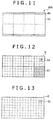
- Fig. 11 illustrates a configuration example of the edge-light backlight 40B.
- the backlight 40B has a plurality of (four in this example) light sources 49 on the top and bottom sides of the display screen S. Light emitted from each of these light sources 49 is guided onto the entire surface of an associated partial light-emitting section 43 by a light guide plate and emitted to the liquid crystal display section 30.
- Fig. 12 schematically illustrates the display screen S of the display device 1B.
- the display screen S is divided into a plurality of partial display areas 33 each of which is associated with one of the partial light-emitting sections 43 ( Fig. 11 ) of the backlight 40B. Further, each of the partial display areas 33 is divided into the plurality of unit areas 32 (16 unit areas 32 in this case).
- the same advantageous effect as with the display device 1 according to the above embodiment can be achieved by using, for example, the correction data map MAP shown in Fig. 6 .
- the backlight 40 having the plurality of partial light-emitting sections 41 is used.
- the present disclosure is not limited thereto. Instead, a backlight including a single light-emitting section may be used.
- the display screen S is divided into the plurality of unit areas 32 as illustrated in Fig. 13 . Even in this case, the same advantageous effect as with the display device 1 according to the above embodiment can be achieved by using, for example, the correction data map MAP shown in Fig. 6 .
- the correction data map MAP is fixed.
- the present disclosure is not limited thereto.
- the correction data map MAP may be prepared in such a manner as to be changed according to the operation mode.
- the correction data DT may be set to 1, 0.9 and 0.8 respectively in the areas RA to RC in so-called home use mode, and to 1 in all the areas RA to RC in image quality priority mode.
- the layout of the areas RA to RC in the display screen S and the number thereof may be changed.
- correction data map may be prepared in such a manner as to be changed according to the video source content.
- a description will be given below of a display device 1F according to the present modification example.
- Fig. 14 illustrates a configuration example of the display device 1F.
- the display device 1F includes a signal processing section 10F.
- the signal processing section 10F includes a content detection portion 15 and peak level correction portion 12F.
- the content detection portion 15 detects content based on content information (e.g., information representing genres such as sports, news, cinemas and animations).
- the peak level correction portion 12F can change the correction data map MAP based on the detection result of the content detection portion 15. More specifically, the peak level correction portion 12F selects the correction data map MAP suitable for the content from among the plurality of preset correction data maps MAP.
- the correction data map MAP used to display a sport program may be, for example, as shown in Fig. 6 .
- the correction data map MAP used to display a cinema program may be, for example, that in which the correction data DT is set to 1 for all the areas RA to RC.
- the content detection portion 15 detects content based on content information contained in the video signal Sdisp.
- content may be detected, for example, based on an EPG (Electronic Program Guide).
- each of the partial display areas 31 is not divided into the plurality of unit areas 32 so that each partial display area is associated one-to-one with a unit area. It should be noted that the components that are substantially the same as those of the display device 1 according to the first embodiment are denoted by the same reference symbols, and that the description thereof will be omitted as appropriate.
- the display device 2 includes a signal processing section 60 as illustrated in Fig. 1 .
- the signal processing section 60 includes a peak level detection portion 61 and peak level correction portion 62.
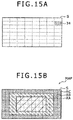
- Fig. 15A schematically illustrates the display screen S of the display device 2, and Fig. 15B an example of the correction data map MAP.
- the display screen S of the display device 2 is divided into partial display areas 34 that are arranged in a matrix form as illustrated in Fig. 15A .
- Each of the partial display areas 34 is associated with one of the partial light-emitting sections 41 of the backlight 40.
- each of the partial display areas 34 is not divided into a plurality of unit areas. Therefore, each of the partial display areas 34 is associated one-to-one with a unit area.
- the correction data DT is set for each of the unit areas 32. Further, in the correction data map MAP according to the display device 2, the correction data DT is set for each of the partial display areas (unit areas) 34 as illustrated in Fig. 15B .
- the peak level detection portion 61 detects the peak level PL of the video signal Sdisp for each of the partial display areas 34, supplying the detection result to the peak level correction portion 62 together with a position PR of the partial display area 34. That is, unlike the peak level detection portion 11 according to the first embodiment, the peak level detection portion 61 supplies the position PR of the partial display area 34 rather than the peak position PP to the peak level correction portion 62.
- the peak level correction portion 62 corrects the peak level PL using the correction data map MAP based on the peak level PL and position PR for each of the partial display areas 34 supplied from the peak level detection portion 61. More specifically, the peak level correction portion 62 acquires the correction data DT in the partial display area (unit area) 34 indicated by the position PR first using the correction data map MAP. Then, the peak level correction portion 62 multiplies the correction data DT by the peak level PL in the partial display area 31 including that unit area 32, thus correcting the peak level PL and generating the peak level PL2. Then, the peak level correction portion 62 finds the gain factor G1 using the function F1 based on the peak level PL2 and also finds the luminance factor G2 using the function F2.
- each of the partial display areas is associated one-to-one with a unit area. Therefore, even if a piece of hardware having poor arithmetic capability is used as the signal processing section, it is possible to provide a high degree of freedom in power control.
- Other advantageous effects of the present embodiment are the same as those of the first embodiment.
- modification examples 1-1, 1-2 and 1-4 of the first embodiment may be applied to the display device 2 according to the present embodiment.
- the correction data map MAP can be dynamically changed based on the video signal Sdisp in the display device 1 according to the first embodiment. It should be noted that the components that are substantially the same as those of the display device 1 according to the first embodiment are denoted by the same reference symbols, and that the description thereof will be omitted as appropriate.
- Fig. 16 illustrates a configuration example of the display device 3 according to the present embodiment.
- the display device 3 includes a signal processing section 50.
- the signal processing section 50 includes a face detection portion 51, correction data map generation portion 53 and peak level correction portion 52.
- the face detection portion 51 detects a human face to be displayed on the display screen S and finds the position and size of the face in the display screen S based on the video signal Sdisp, thus supplying these pieces of information (face detection information IF) to the correction data map generation portion 53.
- the correction data map generation portion 53 generates the correction data map MAP based on the face detection information IF.
- the peak level correction portion 52 corrects the peak level PL detected by the peak level detection portion 11 using the correction data map MAP supplied from the correction data map generation portion 53, thus generating the peak level PL2 and finding the gain factor G1 and luminance factor G2 based on the peak level PL2.
- Fig. 17 illustrates an example of the correction data map MAP according to the present embodiment.
- the correction data map generation portion 53 generates the correction data map MAP based on the face detection information IF. More specifically, the correction data map generation portion 53 sets the area associated with the detected face as the area RA, sets the area RB in such a manner as to surround the area RA and sets the area other than the areas RA and RB as the area RC, thus generating the correction data map MAP.
- the correction data DT is set to "1.0" in the area RA, to "0.9” in the area RB, and to "0.8" in the area RC as in the first embodiment. That is, the power consumption of the partial display areas 31 of the area RA can be reduced without degrading the image quality. On the other hand, the power consumption of the partial display areas 31 of the areas RB and RC can be further reduced at the somewhat expense of image quality.
- the display device 3 detects a human face to be displayed on the display screen S based on the video signal Sdisp, thus setting the area associated with the detected face as the area RA. That is, if the viewer watches, for example, a drama, it is generally likely that the face of the displayed person will attract the attention of the viewer. Further, it is more likely that a color shift, for example, will appear unnatural to the viewer when the face of a person is displayed than when an object is displayed. Therefore, the display device 3 detects a human face and sets the display area thereof as the area RA, thus making it possible to display the face without degrading the image quality.
- the display device 3 sets the areas RB and RC in such a manner as to surround the face display area. That is, it is likely that the human face will attract the attention of the viewer as described above, and it is unlikely that the areas other than the face will attract the attention of the viewer. Therefore, it is unlikely that the viewer will perceive the degradation of image quality even in the event of a color shift in any of the areas other than the face. Therefore, the display device 3 sets the areas other than the face display area as the areas RB and RC, providing reduced power consumption in an effective manner while at the same time minimizing or at least reducing the likelihood of the viewer perceiving the degradation of image quality.
- a correction data map is dynamically generated based on a video signal, thus providing a high degree of freedom in power control according to the display content.
- the face detection section is provided in the present embodiment so that the area showing a face is displayed with high image quality, and that the power consumption of other areas is reduced, thus providing reduced power consumption in an effective manner while at the same time minimizing or at least reducing the likelihood of the viewer perceiving the degradation of image quality.
- a human face to be displayed on the display screen S is detected in the above embodiment.
- the present disclosure is not limited thereto.
- subtitles and telops may be detected. This makes it possible to display subtitles and telops, i.e., information that is likely to attract the attention of the viewer, without degrading the image quality.
- the display area thereof is set as the area RA.
- the present disclosure is not limited thereto. Instead, what is unlikely to attract the attention of the viewer may be detected so that the display area thereof is set as the area RC. More specifically, if the display device 3 is used, for example, for a TV conference system, the display area of one's own face can be set as the area RC. This makes it possible to display the area showing the face of the party on the other end with high image quality and reduce the power consumption of the area showing one's own face at the expense of image quality.
- modification examples 1-1 to 1-4 of the first embodiment may be applied to the display device 3 according to the present embodiment.
- the correction data map MAP can be dynamically changed in the display device 1 according to the first embodiment.
- the present disclosure is not limited thereto.
- the correction data map MAP can be dynamically changed in the display device 2 according to the second embodiment.
- the position of the detected face is set as the area RA, and the areas RB and RC are set in such a manner as to surround the face display area.
- the area in which a face is detected may also be set as the area RA in the correction data map MAP (for example, Fig. 6 ) according to the first and second embodiments as illustrated in Fig. 18 .
- the display device 3 operates in the same manner as the display devices 1 and 2 according to the first and second embodiments if no face is displayed on the display screen S.
- the power consumption of the area showing the face can be reduced in an effective manner without degrading the image quality.
Landscapes
- Engineering & Computer Science (AREA)
- Physics & Mathematics (AREA)
- Computer Hardware Design (AREA)
- General Physics & Mathematics (AREA)
- Theoretical Computer Science (AREA)
- Chemical & Material Sciences (AREA)
- Crystallography & Structural Chemistry (AREA)
- Control Of Indicators Other Than Cathode Ray Tubes (AREA)
- Liquid Crystal (AREA)
- Liquid Crystal Display Device Control (AREA)
Applications Claiming Priority (2)
| Application Number | Priority Date | Filing Date | Title |
|---|---|---|---|
| JP2011246770A JP2013104912A (ja) | 2011-11-10 | 2011-11-10 | 表示装置および表示方法 |
| EP12191148.1A EP2592618B1 (en) | 2011-11-10 | 2012-11-02 | Display device and display method |
Related Parent Applications (2)
| Application Number | Title | Priority Date | Filing Date |
|---|---|---|---|
| EP12191148.1A Division EP2592618B1 (en) | 2011-11-10 | 2012-11-02 | Display device and display method |
| EP12191148.1A Division-Into EP2592618B1 (en) | 2011-11-10 | 2012-11-02 | Display device and display method |
Publications (1)
| Publication Number | Publication Date |
|---|---|
| EP3506249A1 true EP3506249A1 (en) | 2019-07-03 |
Family
ID=47428472
Family Applications (2)
| Application Number | Title | Priority Date | Filing Date |
|---|---|---|---|
| EP12191148.1A Not-in-force EP2592618B1 (en) | 2011-11-10 | 2012-11-02 | Display device and display method |
| EP19158011.7A Withdrawn EP3506249A1 (en) | 2011-11-10 | 2012-11-02 | Display device and display method |
Family Applications Before (1)
| Application Number | Title | Priority Date | Filing Date |
|---|---|---|---|
| EP12191148.1A Not-in-force EP2592618B1 (en) | 2011-11-10 | 2012-11-02 | Display device and display method |
Country Status (4)
| Country | Link |
|---|---|
| US (3) | US9159273B2 (enExample) |
| EP (2) | EP2592618B1 (enExample) |
| JP (1) | JP2013104912A (enExample) |
| CN (1) | CN103106879B (enExample) |
Families Citing this family (14)
| Publication number | Priority date | Publication date | Assignee | Title |
|---|---|---|---|---|
| JP2013104912A (ja) * | 2011-11-10 | 2013-05-30 | Sony Corp | 表示装置および表示方法 |
| KR102074719B1 (ko) * | 2013-10-08 | 2020-02-07 | 엘지디스플레이 주식회사 | 유기 발광 표시 장치 |
| JP6326219B2 (ja) * | 2013-11-26 | 2018-05-16 | 圭祐 戸田 | 表示装置および表示方法 |
| CN106133820B (zh) * | 2014-03-20 | 2018-12-21 | 富士胶片株式会社 | 显示装置以及取景器装置 |
| JP6213341B2 (ja) | 2014-03-28 | 2017-10-18 | ソニー株式会社 | 画像処理装置、画像処理方法、およびプログラム |
| EP3128506A4 (en) | 2014-03-31 | 2017-12-06 | Sony Corporation | Image processing device, image processing method, and program |
| JP6165681B2 (ja) * | 2014-06-27 | 2017-07-19 | 富士フイルム株式会社 | 画像表示装置及び画像表示方法 |
| US10089938B2 (en) * | 2015-06-03 | 2018-10-02 | Japan Display Inc. | Display device with sidelight illumination and luminance correction |
| US10114447B2 (en) * | 2015-12-10 | 2018-10-30 | Samsung Electronics Co., Ltd. | Image processing method and apparatus for operating in low-power mode |
| CN109313793A (zh) | 2016-01-18 | 2019-02-05 | 维弗施福特有限责任公司 | 评估并降低电子显示器的近视源性效应 |
| CN105931612B (zh) * | 2016-07-13 | 2018-12-21 | 京东方科技集团股份有限公司 | 源极驱动电路、方法及显示装置 |
| CN107665681B (zh) * | 2017-09-26 | 2020-06-05 | 武汉华星光电技术有限公司 | 液晶显示器驱动方法、系统及计算机可读取介质 |
| JP2021144066A (ja) * | 2018-06-15 | 2021-09-24 | シャープ株式会社 | 制御装置、表示装置および制御方法 |
| WO2020058034A1 (en) * | 2018-09-18 | 2020-03-26 | Signify Holding B.V. | Pixelated color tunable luminaire |
Citations (6)
| Publication number | Priority date | Publication date | Assignee | Title |
|---|---|---|---|---|
| EP1564478A1 (en) * | 2002-10-22 | 2005-08-17 | Sharp Kabushiki Kaisha | Backlight unit and liquid crystal display unit using backlight unit |
| US20060238487A1 (en) * | 2005-03-29 | 2006-10-26 | Ming-Chia Shih | Display device and method |
| JP2009042652A (ja) | 2007-08-10 | 2009-02-26 | Victor Co Of Japan Ltd | 液晶表示装置及びこれに用いる映像表示方法 |
| EP2154673A2 (en) * | 2008-08-12 | 2010-02-17 | Victor Company of Japan, Limited | Liquid crystal display device and image display method thereof |
| JP2010113099A (ja) | 2008-11-05 | 2010-05-20 | Sharp Corp | 表示装置および表示制御方法 |
| JP2011246770A (ja) | 2010-05-27 | 2011-12-08 | Nippon Steel Corp | 方向性電磁鋼板及び張力絶縁膜被覆方向性電磁鋼板 |
Family Cites Families (9)
| Publication number | Priority date | Publication date | Assignee | Title |
|---|---|---|---|---|
| JP4029743B2 (ja) * | 2003-02-24 | 2008-01-09 | ソニー株式会社 | バックライト |
| JP2008176211A (ja) * | 2007-01-22 | 2008-07-31 | Hitachi Ltd | 液晶表示装置及びその輝度制御方法 |
| US8139022B2 (en) * | 2007-05-08 | 2012-03-20 | Victor Company Of Japan, Limited | Liquid crystal display device and image display method thereof |
| KR100885285B1 (ko) | 2007-05-08 | 2009-02-23 | 닛뽕빅터 가부시키가이샤 | 액정 표시 장치 및 이에 이용되는 영상 표시 방법 |
| KR20090044292A (ko) * | 2007-10-31 | 2009-05-07 | 삼성전자주식회사 | 표시 장치 및 이의 구동방법 |
| KR100959594B1 (ko) * | 2008-05-01 | 2010-05-27 | 닛뽕빅터 가부시키가이샤 | 액정 표시 장치 및 이에 이용되는 영상 표시 방법 |
| JP5495025B2 (ja) * | 2009-12-22 | 2014-05-21 | ソニー株式会社 | 画像処理装置および方法、並びにプログラム |
| JP5661336B2 (ja) * | 2010-05-28 | 2015-01-28 | 日立マクセル株式会社 | 液晶表示装置 |
| JP2013104912A (ja) * | 2011-11-10 | 2013-05-30 | Sony Corp | 表示装置および表示方法 |
-
2011
- 2011-11-10 JP JP2011246770A patent/JP2013104912A/ja not_active Abandoned
-
2012
- 2012-11-02 CN CN201210433438.XA patent/CN103106879B/zh not_active Expired - Fee Related
- 2012-11-02 EP EP12191148.1A patent/EP2592618B1/en not_active Not-in-force
- 2012-11-02 US US13/667,529 patent/US9159273B2/en not_active Expired - Fee Related
- 2012-11-02 EP EP19158011.7A patent/EP3506249A1/en not_active Withdrawn
-
2015
- 2015-09-03 US US14/844,144 patent/US9583052B2/en not_active Expired - Fee Related
-
2017
- 2017-01-19 US US15/409,994 patent/US9922602B2/en active Active
Patent Citations (6)
| Publication number | Priority date | Publication date | Assignee | Title |
|---|---|---|---|---|
| EP1564478A1 (en) * | 2002-10-22 | 2005-08-17 | Sharp Kabushiki Kaisha | Backlight unit and liquid crystal display unit using backlight unit |
| US20060238487A1 (en) * | 2005-03-29 | 2006-10-26 | Ming-Chia Shih | Display device and method |
| JP2009042652A (ja) | 2007-08-10 | 2009-02-26 | Victor Co Of Japan Ltd | 液晶表示装置及びこれに用いる映像表示方法 |
| EP2154673A2 (en) * | 2008-08-12 | 2010-02-17 | Victor Company of Japan, Limited | Liquid crystal display device and image display method thereof |
| JP2010113099A (ja) | 2008-11-05 | 2010-05-20 | Sharp Corp | 表示装置および表示制御方法 |
| JP2011246770A (ja) | 2010-05-27 | 2011-12-08 | Nippon Steel Corp | 方向性電磁鋼板及び張力絶縁膜被覆方向性電磁鋼板 |
Also Published As
| Publication number | Publication date |
|---|---|
| US9922602B2 (en) | 2018-03-20 |
| US9583052B2 (en) | 2017-02-28 |
| US9159273B2 (en) | 2015-10-13 |
| EP2592618A1 (en) | 2013-05-15 |
| US20170132981A1 (en) | 2017-05-11 |
| CN103106879B (zh) | 2019-08-20 |
| CN103106879A (zh) | 2013-05-15 |
| US20130120475A1 (en) | 2013-05-16 |
| US20150379943A1 (en) | 2015-12-31 |
| EP2592618B1 (en) | 2019-08-14 |
| JP2013104912A (ja) | 2013-05-30 |
Similar Documents
| Publication | Publication Date | Title |
|---|---|---|
| EP2592618B1 (en) | Display device and display method | |
| CN102239513B (zh) | 显示装置、亮度调整装置、背光装置、调整亮度的方法 | |
| US10176745B2 (en) | Data conversion unit and method | |
| JP5460435B2 (ja) | 画像表示装置および画像表示装置の制御方法 | |
| US20100328336A1 (en) | Liquid Crystal Display Wall and Method for Controlling the Same | |
| US9330610B2 (en) | Liquid crystal display device including a backlight unit employing a light source and method for driving the same | |
| US20090115720A1 (en) | Liquid crystal display, liquid crystal display module, and method of driving liquid crystal display | |
| US9183797B2 (en) | Display device and control method for display device | |
| JP2010175913A (ja) | 画像表示装置 | |
| US20120293565A1 (en) | Display apparatus and control method thereof | |
| EP2082391B1 (en) | Liquid crystal display system and method | |
| US8605031B2 (en) | Driving apparatus of backlight module and driving method thereof | |
| JP2009294338A (ja) | 液晶駆動装置 | |
| US20110285758A1 (en) | Image display apparatus | |
| US9368072B2 (en) | Image display device and image display method of a multi-display type with local and global control | |
| KR20100104014A (ko) | 자발광형 디스플레이가 적용된 기기에서 소모 전력을 저감시키기 위한 방법 및 장치 | |
| US20100309109A1 (en) | Local dimming method and display apparatus using the same | |
| JP5111652B2 (ja) | バックライト装置及びバックライト装置の制御方法 | |
| CN100496107C (zh) | 电视接收机中利用反馈调整亮度的装置及其方法 | |
| KR100722035B1 (ko) | 텔레비젼 수상기에서 피드백을 이용한 휘도 조절 장치 및 방법 | |
| JP2011141321A (ja) | 液晶表示装置 |
Legal Events
| Date | Code | Title | Description |
|---|---|---|---|
| PUAI | Public reference made under article 153(3) epc to a published international application that has entered the european phase |
Free format text: ORIGINAL CODE: 0009012 |
|
| STAA | Information on the status of an ep patent application or granted ep patent |
Free format text: STATUS: REQUEST FOR EXAMINATION WAS MADE |
|
| 17P | Request for examination filed |
Effective date: 20190219 |
|
| AC | Divisional application: reference to earlier application |
Ref document number: 2592618 Country of ref document: EP Kind code of ref document: P |
|
| AK | Designated contracting states |
Kind code of ref document: A1 Designated state(s): AL AT BE BG CH CY CZ DE DK EE ES FI FR GB GR HR HU IE IS IT LI LT LU LV MC MK MT NL NO PL PT RO RS SE SI SK SM TR |
|
| GRAP | Despatch of communication of intention to grant a patent |
Free format text: ORIGINAL CODE: EPIDOSNIGR1 |
|
| STAA | Information on the status of an ep patent application or granted ep patent |
Free format text: STATUS: GRANT OF PATENT IS INTENDED |
|
| INTG | Intention to grant announced |
Effective date: 20210428 |
|
| RAP3 | Party data changed (applicant data changed or rights of an application transferred) |
Owner name: SONY GROUP CORPORATION |
|
| GRAJ | Information related to disapproval of communication of intention to grant by the applicant or resumption of examination proceedings by the epo deleted |
Free format text: ORIGINAL CODE: EPIDOSDIGR1 |
|
| STAA | Information on the status of an ep patent application or granted ep patent |
Free format text: STATUS: REQUEST FOR EXAMINATION WAS MADE |
|
| INTC | Intention to grant announced (deleted) | ||
| STAA | Information on the status of an ep patent application or granted ep patent |
Free format text: STATUS: EXAMINATION IS IN PROGRESS |
|
| 17Q | First examination report despatched |
Effective date: 20210924 |
|
| STAA | Information on the status of an ep patent application or granted ep patent |
Free format text: STATUS: THE APPLICATION IS DEEMED TO BE WITHDRAWN |
|
| 18D | Application deemed to be withdrawn |
Effective date: 20230601 |