EP3506000A1 - Structure de guide d'onde semi-conducteur iii-v nanoridge - Google Patents
Structure de guide d'onde semi-conducteur iii-v nanoridge Download PDFInfo
- Publication number
- EP3506000A1 EP3506000A1 EP17211015.7A EP17211015A EP3506000A1 EP 3506000 A1 EP3506000 A1 EP 3506000A1 EP 17211015 A EP17211015 A EP 17211015A EP 3506000 A1 EP3506000 A1 EP 3506000A1
- Authority
- EP
- European Patent Office
- Prior art keywords
- iii
- waveguide
- semiconductor
- contact
- freestanding
- Prior art date
- Legal status (The legal status is an assumption and is not a legal conclusion. Google has not performed a legal analysis and makes no representation as to the accuracy of the status listed.)
- Granted
Links
- 239000004065 semiconductor Substances 0.000 title claims abstract description 111
- 229910052710 silicon Inorganic materials 0.000 claims description 74
- 239000010703 silicon Substances 0.000 claims description 72
- 239000000463 material Substances 0.000 claims description 47
- 239000000758 substrate Substances 0.000 claims description 43
- 229910001218 Gallium arsenide Inorganic materials 0.000 claims description 30
- 238000000034 method Methods 0.000 claims description 23
- 239000002096 quantum dot Substances 0.000 claims description 20
- 229910000530 Gallium indium arsenide Inorganic materials 0.000 claims description 17
- RPQDHPTXJYYUPQ-UHFFFAOYSA-N indium arsenide Chemical class [In]#[As] RPQDHPTXJYYUPQ-UHFFFAOYSA-N 0.000 claims description 12
- 238000004519 manufacturing process Methods 0.000 claims description 11
- 238000002161 passivation Methods 0.000 claims description 10
- HQVNEWCFYHHQES-UHFFFAOYSA-N silicon nitride Chemical compound N12[Si]34N5[Si]62N3[Si]51N64 HQVNEWCFYHHQES-UHFFFAOYSA-N 0.000 claims description 10
- 229910052581 Si3N4 Inorganic materials 0.000 claims description 9
- 238000011065 in-situ storage Methods 0.000 claims description 7
- 229910000673 Indium arsenide Inorganic materials 0.000 claims description 5
- 229910005542 GaSb Inorganic materials 0.000 claims description 4
- 230000008878 coupling Effects 0.000 claims description 4
- 238000010168 coupling process Methods 0.000 claims description 4
- 238000005859 coupling reaction Methods 0.000 claims description 4
- 230000005855 radiation Effects 0.000 claims description 3
- XUIMIQQOPSSXEZ-UHFFFAOYSA-N Silicon Chemical compound [Si] XUIMIQQOPSSXEZ-UHFFFAOYSA-N 0.000 description 69
- 230000008901 benefit Effects 0.000 description 26
- 230000003287 optical effect Effects 0.000 description 20
- 238000010521 absorption reaction Methods 0.000 description 11
- 229910052751 metal Inorganic materials 0.000 description 11
- 239000002184 metal Substances 0.000 description 11
- 238000002347 injection Methods 0.000 description 10
- 239000007924 injection Substances 0.000 description 10
- VYPSYNLAJGMNEJ-UHFFFAOYSA-N Silicium dioxide Chemical compound O=[Si]=O VYPSYNLAJGMNEJ-UHFFFAOYSA-N 0.000 description 9
- 229910052814 silicon oxide Inorganic materials 0.000 description 9
- 230000007547 defect Effects 0.000 description 8
- 239000013078 crystal Substances 0.000 description 6
- 230000010354 integration Effects 0.000 description 6
- 230000008569 process Effects 0.000 description 6
- WGTYBPLFGIVFAS-UHFFFAOYSA-M tetramethylammonium hydroxide Chemical compound [OH-].C[N+](C)(C)C WGTYBPLFGIVFAS-UHFFFAOYSA-M 0.000 description 6
- 208000012868 Overgrowth Diseases 0.000 description 5
- 238000000151 deposition Methods 0.000 description 5
- 238000000059 patterning Methods 0.000 description 5
- 239000002019 doping agent Substances 0.000 description 4
- 230000006798 recombination Effects 0.000 description 4
- 238000005215 recombination Methods 0.000 description 4
- 230000015572 biosynthetic process Effects 0.000 description 3
- 230000001419 dependent effect Effects 0.000 description 3
- 230000008021 deposition Effects 0.000 description 3
- 238000005530 etching Methods 0.000 description 3
- 239000012212 insulator Substances 0.000 description 3
- 238000001459 lithography Methods 0.000 description 3
- 239000000203 mixture Substances 0.000 description 3
- 238000005498 polishing Methods 0.000 description 3
- 239000002243 precursor Substances 0.000 description 3
- 238000000927 vapour-phase epitaxy Methods 0.000 description 3
- 230000004888 barrier function Effects 0.000 description 2
- 238000010586 diagram Methods 0.000 description 2
- 230000000694 effects Effects 0.000 description 2
- 238000000407 epitaxy Methods 0.000 description 2
- 229910052732 germanium Inorganic materials 0.000 description 2
- 238000001451 molecular beam epitaxy Methods 0.000 description 2
- 238000010899 nucleation Methods 0.000 description 2
- 230000009467 reduction Effects 0.000 description 2
- 238000004088 simulation Methods 0.000 description 2
- 230000007704 transition Effects 0.000 description 2
- UFHFLCQGNIYNRP-UHFFFAOYSA-N Hydrogen Chemical compound [H][H] UFHFLCQGNIYNRP-UHFFFAOYSA-N 0.000 description 1
- 229910000577 Silicon-germanium Inorganic materials 0.000 description 1
- 230000009471 action Effects 0.000 description 1
- 230000004913 activation Effects 0.000 description 1
- 239000011149 active material Substances 0.000 description 1
- 230000003321 amplification Effects 0.000 description 1
- 239000000969 carrier Substances 0.000 description 1
- 239000012159 carrier gas Substances 0.000 description 1
- 239000010949 copper Substances 0.000 description 1
- 238000001514 detection method Methods 0.000 description 1
- 229910003460 diamond Inorganic materials 0.000 description 1
- 239000010432 diamond Substances 0.000 description 1
- 230000005684 electric field Effects 0.000 description 1
- 238000000605 extraction Methods 0.000 description 1
- 239000007789 gas Substances 0.000 description 1
- GNPVGFCGXDBREM-UHFFFAOYSA-N germanium atom Chemical compound [Ge] GNPVGFCGXDBREM-UHFFFAOYSA-N 0.000 description 1
- 230000006872 improvement Effects 0.000 description 1
- 239000012535 impurity Substances 0.000 description 1
- 229910052738 indium Inorganic materials 0.000 description 1
- 238000001465 metallisation Methods 0.000 description 1
- 229910021421 monocrystalline silicon Inorganic materials 0.000 description 1
- 150000004767 nitrides Chemical class 0.000 description 1
- 230000006911 nucleation Effects 0.000 description 1
- 238000003199 nucleic acid amplification method Methods 0.000 description 1
- 230000005693 optoelectronics Effects 0.000 description 1
- 239000012071 phase Substances 0.000 description 1
- 238000005086 pumping Methods 0.000 description 1
- 230000005701 quantum confined stark effect Effects 0.000 description 1
- 239000000243 solution Substances 0.000 description 1
- 239000000126 substance Substances 0.000 description 1
- 230000008685 targeting Effects 0.000 description 1
- WFKWXMTUELFFGS-UHFFFAOYSA-N tungsten Chemical compound [W] WFKWXMTUELFFGS-UHFFFAOYSA-N 0.000 description 1
- 229910052721 tungsten Inorganic materials 0.000 description 1
- 239000010937 tungsten Substances 0.000 description 1
Images


Classifications
-
- G—PHYSICS
- G02—OPTICS
- G02F—OPTICAL DEVICES OR ARRANGEMENTS FOR THE CONTROL OF LIGHT BY MODIFICATION OF THE OPTICAL PROPERTIES OF THE MEDIA OF THE ELEMENTS INVOLVED THEREIN; NON-LINEAR OPTICS; FREQUENCY-CHANGING OF LIGHT; OPTICAL LOGIC ELEMENTS; OPTICAL ANALOGUE/DIGITAL CONVERTERS
- G02F1/00—Devices or arrangements for the control of the intensity, colour, phase, polarisation or direction of light arriving from an independent light source, e.g. switching, gating or modulating; Non-linear optics
- G02F1/01—Devices or arrangements for the control of the intensity, colour, phase, polarisation or direction of light arriving from an independent light source, e.g. switching, gating or modulating; Non-linear optics for the control of the intensity, phase, polarisation or colour
- G02F1/015—Devices or arrangements for the control of the intensity, colour, phase, polarisation or direction of light arriving from an independent light source, e.g. switching, gating or modulating; Non-linear optics for the control of the intensity, phase, polarisation or colour based on semiconductor elements with at least one potential jump barrier, e.g. PN, PIN junction
- G02F1/017—Structures with periodic or quasi periodic potential variation, e.g. superlattices, quantum wells
- G02F1/01708—Structures with periodic or quasi periodic potential variation, e.g. superlattices, quantum wells in an optical wavequide structure
-
- G—PHYSICS
- G02—OPTICS
- G02B—OPTICAL ELEMENTS, SYSTEMS OR APPARATUS
- G02B6/00—Light guides; Structural details of arrangements comprising light guides and other optical elements, e.g. couplings
- G02B6/10—Light guides; Structural details of arrangements comprising light guides and other optical elements, e.g. couplings of the optical waveguide type
- G02B6/12—Light guides; Structural details of arrangements comprising light guides and other optical elements, e.g. couplings of the optical waveguide type of the integrated circuit kind
- G02B6/13—Integrated optical circuits characterised by the manufacturing method
- G02B6/131—Integrated optical circuits characterised by the manufacturing method by using epitaxial growth
-
- G—PHYSICS
- G02—OPTICS
- G02F—OPTICAL DEVICES OR ARRANGEMENTS FOR THE CONTROL OF LIGHT BY MODIFICATION OF THE OPTICAL PROPERTIES OF THE MEDIA OF THE ELEMENTS INVOLVED THEREIN; NON-LINEAR OPTICS; FREQUENCY-CHANGING OF LIGHT; OPTICAL LOGIC ELEMENTS; OPTICAL ANALOGUE/DIGITAL CONVERTERS
- G02F1/00—Devices or arrangements for the control of the intensity, colour, phase, polarisation or direction of light arriving from an independent light source, e.g. switching, gating or modulating; Non-linear optics
- G02F1/01—Devices or arrangements for the control of the intensity, colour, phase, polarisation or direction of light arriving from an independent light source, e.g. switching, gating or modulating; Non-linear optics for the control of the intensity, phase, polarisation or colour
- G02F1/015—Devices or arrangements for the control of the intensity, colour, phase, polarisation or direction of light arriving from an independent light source, e.g. switching, gating or modulating; Non-linear optics for the control of the intensity, phase, polarisation or colour based on semiconductor elements with at least one potential jump barrier, e.g. PN, PIN junction
- G02F1/025—Devices or arrangements for the control of the intensity, colour, phase, polarisation or direction of light arriving from an independent light source, e.g. switching, gating or modulating; Non-linear optics for the control of the intensity, phase, polarisation or colour based on semiconductor elements with at least one potential jump barrier, e.g. PN, PIN junction in an optical waveguide structure
-
- G—PHYSICS
- G02—OPTICS
- G02F—OPTICAL DEVICES OR ARRANGEMENTS FOR THE CONTROL OF LIGHT BY MODIFICATION OF THE OPTICAL PROPERTIES OF THE MEDIA OF THE ELEMENTS INVOLVED THEREIN; NON-LINEAR OPTICS; FREQUENCY-CHANGING OF LIGHT; OPTICAL LOGIC ELEMENTS; OPTICAL ANALOGUE/DIGITAL CONVERTERS
- G02F1/00—Devices or arrangements for the control of the intensity, colour, phase, polarisation or direction of light arriving from an independent light source, e.g. switching, gating or modulating; Non-linear optics
- G02F1/01—Devices or arrangements for the control of the intensity, colour, phase, polarisation or direction of light arriving from an independent light source, e.g. switching, gating or modulating; Non-linear optics for the control of the intensity, phase, polarisation or colour
- G02F1/21—Devices or arrangements for the control of the intensity, colour, phase, polarisation or direction of light arriving from an independent light source, e.g. switching, gating or modulating; Non-linear optics for the control of the intensity, phase, polarisation or colour by interference
- G02F1/225—Devices or arrangements for the control of the intensity, colour, phase, polarisation or direction of light arriving from an independent light source, e.g. switching, gating or modulating; Non-linear optics for the control of the intensity, phase, polarisation or colour by interference in an optical waveguide structure
-
- G—PHYSICS
- G02—OPTICS
- G02B—OPTICAL ELEMENTS, SYSTEMS OR APPARATUS
- G02B6/00—Light guides; Structural details of arrangements comprising light guides and other optical elements, e.g. couplings
- G02B6/10—Light guides; Structural details of arrangements comprising light guides and other optical elements, e.g. couplings of the optical waveguide type
- G02B6/12—Light guides; Structural details of arrangements comprising light guides and other optical elements, e.g. couplings of the optical waveguide type of the integrated circuit kind
- G02B2006/12083—Constructional arrangements
- G02B2006/12097—Ridge, rib or the like
-
- G—PHYSICS
- G02—OPTICS
- G02B—OPTICAL ELEMENTS, SYSTEMS OR APPARATUS
- G02B6/00—Light guides; Structural details of arrangements comprising light guides and other optical elements, e.g. couplings
- G02B6/10—Light guides; Structural details of arrangements comprising light guides and other optical elements, e.g. couplings of the optical waveguide type
- G02B6/12—Light guides; Structural details of arrangements comprising light guides and other optical elements, e.g. couplings of the optical waveguide type of the integrated circuit kind
- G02B2006/12083—Constructional arrangements
- G02B2006/12128—Multiple Quantum Well [MQW]
-
- G—PHYSICS
- G02—OPTICS
- G02B—OPTICAL ELEMENTS, SYSTEMS OR APPARATUS
- G02B6/00—Light guides; Structural details of arrangements comprising light guides and other optical elements, e.g. couplings
- G02B6/10—Light guides; Structural details of arrangements comprising light guides and other optical elements, e.g. couplings of the optical waveguide type
- G02B6/12—Light guides; Structural details of arrangements comprising light guides and other optical elements, e.g. couplings of the optical waveguide type of the integrated circuit kind
- G02B2006/12166—Manufacturing methods
- G02B2006/12178—Epitaxial growth
-
- G—PHYSICS
- G02—OPTICS
- G02F—OPTICAL DEVICES OR ARRANGEMENTS FOR THE CONTROL OF LIGHT BY MODIFICATION OF THE OPTICAL PROPERTIES OF THE MEDIA OF THE ELEMENTS INVOLVED THEREIN; NON-LINEAR OPTICS; FREQUENCY-CHANGING OF LIGHT; OPTICAL LOGIC ELEMENTS; OPTICAL ANALOGUE/DIGITAL CONVERTERS
- G02F1/00—Devices or arrangements for the control of the intensity, colour, phase, polarisation or direction of light arriving from an independent light source, e.g. switching, gating or modulating; Non-linear optics
- G02F1/01—Devices or arrangements for the control of the intensity, colour, phase, polarisation or direction of light arriving from an independent light source, e.g. switching, gating or modulating; Non-linear optics for the control of the intensity, phase, polarisation or colour
- G02F1/015—Devices or arrangements for the control of the intensity, colour, phase, polarisation or direction of light arriving from an independent light source, e.g. switching, gating or modulating; Non-linear optics for the control of the intensity, phase, polarisation or colour based on semiconductor elements with at least one potential jump barrier, e.g. PN, PIN junction
- G02F1/017—Structures with periodic or quasi periodic potential variation, e.g. superlattices, quantum wells
- G02F1/01791—Quantum boxes or quantum dots
Definitions
- the present invention relates to photonic systems. More particularly, the present invention relates to III-V semiconductor nanoridge waveguide structures with efficient current injection and/or limited non-radiative recombination as well as to methods of making them.
- Photonics systems are widely spread. They are advantageously used for implementing optical or electro-optical functionalities in a compact way.
- One of highly prospective photonics systems targeting tele- and datacom as well as optical sensing, is the emerging platform based on silicon.
- Silicon photonics leverages the CMOS manufacturing infrastructure to realize photonic integrated circuits, typically using indirect bandgap group-IV semiconductor materials to realize passive waveguide functionality as well as active electro-optical functionality such as light modulation and light detection.
- III-V semiconductor nanoridge waveguide structures are photonic structures that are particularly useful for forming active waveguides on a monolithic integrated photonics system. Nevertheless, such III-V semiconductor nanoridge waveguide structures currently still suffer from limited injection efficiency and loss of efficiency due to radiative combination.
- III-V semiconductor nanoridge waveguides with a good current injection efficiency and/or limited non-radiative recombination, as well as monolithically integrated photonic devices comprising such III-V semiconductor nanoridge waveguides and methods for producing such III-V semiconductor nanoridge waveguides.
- the present invention relates to a III-V semiconductor waveguide, the III-V semiconductor waveguide being a nanoridge structure having a narrow supporting base with a freestanding wider body portion on top, the III-V semiconductor waveguide comprising a PIN diode, the III-V semiconductor waveguide comprising
- the III-V semiconductor nanoridge waveguides can be seeded on the ⁇ 111 ⁇ facets of a V-shaped silicon surface as said ⁇ 111 ⁇ facets of said silicon surface exclude the presence of antiphase boundaries.
- the deposition can also be made on a flat (001) silicon surface.
- the trench side walls can in such embodiments also trap anti phase boundaries.
- the photonics device furthermore may comprise narrow trenches with widths ranging from 20nm to 500nm and with heights ranging from 100nm to 500nm from which the III-V semiconductor waveguide is monolithically grown.
- the photonics device may be a monolithic integrated active/passive waveguide photonic device further comprising a passive waveguide and configured for coupling radiation between the passive waveguide and the active III-V semiconductor waveguide. It is an advantage of particular embodiments of the present invention that it can combine active, direct bandgap III-V material based structures showing better light generation and absorption efficiencies, and passive crystal silicon structures showing low losses on a single platform. It is an advantage of embodiments of the present invention that active III-V material can be directly and selectively grown on a patterned silicon substrate.
- the passive waveguide may be a silicon or silicon nitride waveguide.
- Growing a doped layer may comprise epitaxially growing a layer at least partly wrapping the freestanding wider body portion.
- Monolithically integrating on the substrate a III-V semiconductor nanoridge waveguide may comprise growing the freestanding wider body portion vertically and laterally from a supporting bottom fin portion, said supporting bottom fin portion being in contact with the substrate.
- Monolithically integrating may comprise growing the III-V semiconductor nanoridge waveguide monolithic in narrow trenches with widths ranging from 20 nm to 500 nm and with heights ranging from 100 nm to 500 nm.
- Monolithically integrating may comprise growing the III-V semiconductor nanoridge waveguide seeded on a ⁇ 111 ⁇ facets of a V-shaped Si surface.
- Monolithically integrating may comprise growing the III-V semiconductor nanoridge waveguide by any of metal organic vapor phase epitaxy, molecular beam epitaxy or hybrid vapour phase epitaxy. Integrating may comprise fabricating active III-V nanoridge waveguides comprising each a freestanding body portion and a supporting bottom fin portion, whereby the freestanding body portion is characterized by that part of the nanoridge waveguide which is growing out vertically and laterally from the supporting bottom fin portion of the nanoridge waveguide, said supporting bottom fin portion being in contact with the substrate.
- the present invention relates to a III-V semiconductor nanoridge waveguide structure.
- a III-V semiconductor nanoridge waveguide structure typically has a narrow supporting base with a freestanding wider body portion on top, as described above.
- the III-V waveguide comprises a PIN diode.
- the waveguide comprises a III-V semiconductor waveguide core formed in the freestanding wider body portion and at least one heterojunction incorporated in the III-V semiconductor waveguide core.
- the at least one heterojunction may be one or more active quantum wells or quantum dots, or it may be a heterojunction between bulk materials.
- the waveguide also comprises a bottom doped region of a first polarity positioned at a bottom of the narrow supporting base forming a lower contact, and an upper doped region of a second polarity forming an upper contact.
- Structures according to embodiments of the present invention are characterized in that the upper contact is positioned at at least one side wall of the freestanding wider body portion.
- reference is made to a side wall reference is made to a wall not substantially facing the narrow supporting base.
- the side wall may make an average angle larger than 45° with respect to the plane of the substrate whereon the III-V semiconductor nanoridge waveguide is grown.
- upper contacting may be performed only at a side wall of the freestanding wider body portion.
- contacting may be performed both at one or more side walls of the freestanding wider body portion combined with contacting at a top wall of the freestanding wider body portion.
- the polarity of the upper contact may depend on the orientation of the PIN diode formed.
- the upper contact is an n-type contact and the lower contact is a p-type contact.
- the n-type contact may be a contact fin from n+ implanted silicon.
- the p-type contact may be a contact implemented in an in-situ p+ doped, low bandgap III-V semiconductor fin.
- the upper contact is a p-type contact and the lower contact is an n-type contact.
- the p-type contact may be a contact fin from p+ implanted silicon.
- the n-type contact may be a contact implemented in an in-situ n+ doped, low bandgap III-V semiconductor fin.
- the freestanding wider body portion may have a substantially square shaped or rectangular shaped shape, but alternatively also may have another shape, such as for example a diamond shaped shape, curved shapes etc..
- FIG. 1 a number of examples of possible shapes of the freestanding wider body portion are shown in FIG. 1 , in combination with a number of examples of upper contacts.
- FIG. 1 a plurality of portions of waveguides is shown.
- the waveguide may be a III-V semiconductor waveguide, such as for example GaAs waveguides with InGaAs quantum wells, InAs and InGaAs quantum dots, InGaAs/GaSbAs transitions, InGaNAs quantum wells, or for example InP waveguides with InGaAs quantum wells InGaAsP quantum wells, InAs quantum dots, AlGaInAs quantum wells, or for example InAs with InGaSbAs quantum wells and GaSb with InGaSbAs quantum wells.
- III-V semiconductor waveguide such as for example GaAs waveguides with InGaAs quantum wells, InAs and InGaAs quantum dots, InGaAs/GaSbAs transitions, InGaNAs quantum wells, or for example InP waveguides with InGaAs quantum wells InGaAsP quantum wells, InAs quantum dots, AlGaInAs quantum wells, or
- the quantum wells and quantum dots thereby are strained to the lattice constant of the waveguide material.
- specific wavelength ranges can be used in the photonics device, as shown in table 1.
- the III-V semiconductor waveguides may be implemented as nano ridges.
- III-V materials III-V semiconductor waveguide Active material (providing optical gain)
- Emission wavelength GaAs InGaAs quantum wells In content >25% 1120nm ⁇ 1350nm InAs quantum dots 1120nm ⁇ 1350nm InGaAs/GaSbAs type II transition 1120nm ⁇ 1400nm
- InGaNAs quantum wells dilute nitrides 1250nm ⁇ 1600nm InP or InGaAs InGaAs quantum wells: In content >30% 1250nm ⁇ 1600nm InGaAsP quantum wells 1250nm ⁇ 1700nm InAs quantum dots 1250nm ⁇ 1700nm AlGaInAs quantum wells 1250nm ⁇ 1700nm InAs InGaSbAs - different composition in barrier and quantum well 1550nm ⁇ 5000nm GaSb InGaSbAs - different composition in barrier and quantum well 1550nm ⁇
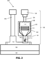
- FIG. 2 shows a III-V waveguide 100 being a nanoridge structure.
- the III-V semiconductor waveguide comprises a narrow supporting base 101 and a freestanding wider body portion 102.
- the waveguide 100 comprises a PIN diode 103, e.g. a vertical PIN diode.
- the III-V waveguide 100 is formed on a substrate comprising a plurality of layers 104, 106.
- the III-V waveguide 100 is grown on a N+ doped GaAs layer 116 comprising crystal defects 114, itself grown on a N+ doped silicon layer 112 acting as a bottom contact 112 in a n+ implanted silicon fin on the substrate.
- the N+ Si and N+ GaAs regions forms the n-type electrode of the III-V semiconductor p-i-n diode 103.
- the III-V waveguide 100 in the present case is III-V waveguide core 110 made of a non-intentionally doped (intrinsic) GaAs material and comprising at least one heterojunction 118, in the present example being one or more InGaAs quantum wells.
- the III-V waveguide 100 furthermore comprises a passivation layer 120, in the present example being an InGaP layer.
- the III-V waveguide 100 also comprises, at the upper side of the III-V waveguide 100, a GaAs layer 122 as well as a P+ doped GaAs layer 124, acting as the p-side electrode of the III-V semiconductor pi-n diode 103.
- table 2 illustrates possible dimensions of the different elements of the III-V waveguide.
- Table 2 Width N+ GaAs 20nm - 100nm Height N+ GaAs 100nm - 400nm Height GaAs waveguide 200nm - 1000nm Width GaAs waveguide 50nm - 500nm Width GaAs top layer 200nm - 600nm Height top electrode 100nm - 500nm Width doped GaAs(+) layer 20nm - 100nm
- an active III-V semiconductor waveguide can be monolithically co-integrated with passive and active silicon/silicon-nitride waveguide devices.
- the III-V / silicon semiconductor device is such that both waveguides are formed directly on a single semiconductor substrate, e.g. a substrate comprising a single silicon layer.
- the photonics device thus may be a monolithic integrated active/passive waveguide photonic device comprising an active and a passive waveguide and being configured for coupling radiation between the passive waveguide and the active III-V semiconductor waveguide.
- the photonic system may in one embodiment comprise a semiconductor optical amplifier comprising a III-V semiconductor nanoridge gain waveguide coupled to passive waveguides using 100% evanescent couplers.
- the photonic system may in another embodiment be for use in a laser diode.
- the photonic system may then comprise a semiconductor optical amplifier, e.g. as described above, with optical gain provide by the forward-biased III-V semiconductor p-i-n waveguide and optical feedback provided by optical mirrors implemented in the III-V semiconductor waveguide or in the passive waveguide(s), e.g. silicon waveguide(s).
- the photonic system may in still another embodiment be a photodetector comprising for example a reverse-biased III-V semiconductor p-i-n absorption waveguide coupled to a passive waveguide, e.g. a silicon waveguide, using 100% evanescent couplers.
- the photonic system may in yet another embodiment be an optical transceiver implementation wherein co-integration is obtained of a laser diode, an electro-absorption modulator, a semiconductor optical amplifier and a photodetector with individually optimized III-V gain/absorption properties and interconnected through passive and active waveguide devices, e.g. silicon waveguide devices.
- the present invention relates to a method for manufacturing a photonics device comprising a III-V semiconductor nanoridge waveguide.
- the method may be especially suitable for manufacturing a system as described in the first aspect.
- the method comprises the steps of providing a substrate and monolithically integrating on the substrate a III-V semiconductor nanoridge waveguide.
- the monolithic integration comprises growing a freestanding wider body portion of III-V semiconductor material and at least one heterojunction forming one or more active quantum wells or quantum dots incorporated therein, and growing a doped layer on at least a sidewall of the freestanding wider body portion for forming a contact on the freestanding wider body portion.
- Growing a doped layer may comprise epitaxially growing a layer at least partly wrapping the freestanding wider body portion.
- FIG. 3 to FIG. 19 an exemplary method of fabrication is described with reference to FIG. 3 to FIG. 19 , illustrating different steps in more detail. Nevertheless, multiple additional processing steps may be inserted alternatively or some processing steps may be skipped, for example in order to achieve good coupling means between an active direct bandgap III-V semiconductor nanoridge waveguides and passive silicon waveguides monolithic integrated in an integrated photonic circuits and devices.
- the method is illustrated with reference to a silicon photonics system. It should be understood that embodiments are not limited thereto.
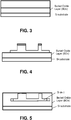
- passive waveguide structures In a first step monocrystalline silicon or silicon nitride layers are patterned to define a plurality of passive waveguide structures. These passive waveguide structures may be the basis for more complex photonic devices, such as Mach-Zehnder interferometers, splitters and combiners, microring resonators, waveguide cavities, grating couplers, tapers, or may even be part of active silicon devices after supplementary processing steps, such as integrated heaters, modulators, photodiodes, phase-shifters, etc.
- the silicon or silicon nitride structures formed based in the silicon or silicon nitride layer are part of the active / passive waveguide structure, may be part of a passive silicon device or an active silicon device.
- the process can be started from a silicon on insulator substrate.
- silicon nitride can be deposited using CVD processing on top of an underlying buried silicon oxide layer and may be 200 nm to 600 nm thick.
- Other passive layers for patterning are also possible.
- the patterning step defining the waveguide structures includes the exposure of a photosensitive mask, its development, and a chemical etch step, which together form a lithographic patterning step to selectively open areas in the substrate layer. In preferred embodiments of the invention, this lithographic patterning step is repeated, so as to obtain defined waveguide structures comprising different etch depths, e.g. fully etched ridge waveguides or partially etched shoulders of a rib waveguide.
- FIG. 3 is showing the substrate and buried oxide layer as well as the silicon or silicon nitride substrate layer.
- FIG. 4 shows the patterning of the silicon or silicon nitride substrate layer.
- the remaining photosensitive material is removed and the etched parts of the patterned substrate layer are filled with silicon oxide or any other suitable isolating material and the resulting surface is planarized, e.g. by chemical-mechanical polishing, to a height level which coincides with the top level of the substrate layer.
- dopants are implanted locally into the well-defined regions of the waveguide structures that were patterned into the silicon substrate layer.
- the dopants may be donors or acceptor impurity species with the effect of locally changing the doping level and therefore locally modifying the majority carrier concentrations within the silicon waveguide regions.
- the implanted dopants may require a subsequent activation step, which for example is achieved through rapid thermal processing.
- a phase-shifter or modulator may require a pn-junction or pin-junction type interface in order to achieve carrier injection or depletion into or out of a silicon waveguide core influencing thereby its absorption coefficient or refractive index.
- Such a junction may be formed by implanting dopants into a first and second shoulder of a silicon rib waveguide so as to obtain a first, n+ doped region, and a second p+ doped region adjacent to the silicon core region.
- a lower contact fin of the final active, direct bandgap III-V semiconductor nanoridge waveguides may be a thin n+ doped silicon fin, preferably between 20 nm to 100 nm wide, and patterned into the silicon substrate such that it does not reach the buried oxide layer underneath the silicon substrate layer. Instead such a n+ doped contact fin is defined on top of a thin, typically 100 nm high basis of residual n+ doped silicon, the residual n+ doped silicon being in contact with an adjacent n+ doped silicon rib structure at one side.
- the lower n+ doped silicon contact fin of the final active, direct bandgap III-V semiconductor nanoridge waveguides typically has heights in the range of 100 nm to 400 nm.
- the said n+ doped silicon fin is adjacent, but not in electrical contact to a dopant-free silicon waveguide at the other side and separated by silicon oxide filled, typically 50 nm to 800 nm wide gap as measured between the center of said n+ doped fin and the closest outer edge of said dopant-free silicon ridge waveguide.
- said dopant-free silicon ridge waveguide is typically 100 nm to 1000 nm wide and 200 nm to 500 nm high, but other geometric shapes and dimensions may be selected for other purposes too.
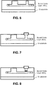
- a thin dielectric liner layer e.g. a thin silicon oxide layer, is deposited on top of all the preceding layers.
- FIG. 6 illustrates deposition of an oxide liner.
- a fifth step recesses are formed locally into said thin silicon oxide liner layer removing completely the deposited silicon oxide liner layer in regions where said lower n+ doped silicon contact fins are located. Typically the width of the recess exceeds the width of the exposed lower n+ doped silicon contact fins.
- FIG. 7 the creation of the local oxide recess is shown.
- n+ doped silicon contact fins of the previous step are anisotropically wet etched, e.g. by addition of the wet etchant tetramethylammonium hydroxide (TMAH).
- TMAH tetramethylammonium hydroxide
- FIG. 8 the application of a TMAH wet silicon fin recess etch is illustrated. It is advantageous of embodiments of the present invention that the choice of the wet etchant, the etchant's concentration and temperature can be controlled so as to achieve smooth, V-shaped etching of silicon seed surfaces having free ⁇ 111 ⁇ facets after the anisotropic wet etch step, which reduces defect formation and excludes the existence of antiphase domain formation upon epitaxial growth of III-V materials on those seeding silicon surfaces.
- the tips of the V-shaped silicon surface pointing toward the substrate may be located at a height level that corresponds to the height of the top level of the residual n+ doped silicon substrate layer of the unetched, lower n+ doped silicon contact fins.
- the thin trenches in the silicon oxide layer that form as result from the wet etch step have their depths maximized and enable high aspect ratios exceeding one, preferably in the range from five to twenty-five.
- Such trenches of high aspect ratios have the advantage of trapping misfit and dislocation defects efficiently as soon as III-V materials are epitaxially grown inside them.
- the trench side walls may be angled in embodiments of the invention.
- a bottom n+ doped, direct bandgap III-V material layer e.g. n+ doped GaAs
- a bottom n+ doped, direct bandgap III-V material layer is grown epitaxially inside said high aspect ratio trenches from which the n+ doped silicon was removed by an anisotropic wet etch in the previous step.
- the latter is shown in FIG. 9 .
- Doping the III-V material layer will improve its contact properties as said n+ doped, direct bandgap III-V material layer epitaxially grown inside the narrow trenches is still forming the lower n+ doped contact fin of the final active, direct bandgap III-V nanoridge waveguide.
- well-studied epitaxial deposition techniques such as low pressure metal organic vapor phase epitaxy (MOVPE) may be used to grow the n+ doped, direct bandgap III-V material layer.
- MOVPE metal organic vapor phase epitaxy
- Known metal organic precursors like TMGa and TBAs may be introduced into a 300 mm MOVPE chamber operating at pressures in the range of 20-100 torr for this purpose, and molecular hydrogen gas may act as carrier gas.
- III-V materials such as doped or intrinsic GaAs, InGaAs, InP, etc.
- III-V materials such as doped or intrinsic GaAs, InGaAs, InP, etc.
- doped or intrinsic GaAs, InGaAs, InP, etc. may be used during this epitaxy step, even though there exists an important lattice mismatch between these III-V materials and silicon.
- said direct bandgap III-V material layer is first seeded on V-shaped silicon surfaces whose facets are oriented ⁇ 111 ⁇ crystal planes; the growth on ⁇ 111 ⁇ silicon crystal planes excludes the formation of antiphase domain boundaries.
- the epitaxial growth of the direct bandgap III-V material layer inside said narrow trenches, e.g. n+ doped GaAs, as described in the seventh step typically involves a sequence of several minor steps.
- a closed and uniform seed layer of n+ doped GaAs is formed on the V-shaped ⁇ 111 ⁇ silicon crystal planes as a result of a low first temperature, 2D nucleation process typically taking place at 350°C-450°C, e.g. at 360°C.
- increasing first temperatures to second temperatures which may vary between 500°C-650°C lead to some reflow of the seed layer which, however, stays closed.
- material overgrowth takes place at said high second temperatures and the narrow trenches are filled by the same or a different III-V material.
- one or more III-V materials are overgrown on top of the trench filling III-V material, the growth temperatures depending on the selected III-V materials during the overgrowth.
- This overgrowth starts at the upper level of the narrow trenches where said recess in the silicon oxide liner layer may be wider than the trench itself.
- intrinsic GaAs may be grown on top of the trench filling, n+ doped GaAs lower contact fin, so as to form the body portion of the final active III-V nanoridge waveguide. It is an advantage of embodiments of the invention that the overgrown III-V material, e.g.
- the GaAs box-like portion are completely relaxed and have free-standing lattice constants, which facilitates their use as buffer for the integration of hetero-layers, e.g. multiple stacked quantum well structures. This is shown in FIG. 10 .
- various shapes of the overgrown III-V material can be obtained depending on the selected process parameters, such as growth temperature, partial pressure of the precursors, III/V ratio of the precursors, reactor pressure, pattern mask ratio, selective area growth rate, growth rates of different III-V compositions and of their respective crystal planes, etc.
- Shapes may be of triangular, box-like, diamond-like, or ridge-like cross-section with a hat-like or a flat top surface.
- the upwards directed Ga-rich ⁇ 111 ⁇ surface of a GaAs III-V material may be subject to growth conditions favoring this surface over other surfaces, e.g. the downwards directed As-rich ⁇ 111 ⁇ layer, the (001) top layer, and the ⁇ 110 ⁇ side layers; these growth conditions lead to quickly forming flat top surfaces and a box-like shapes.
- This box-like shapes with flat top surfaces are of advantage for the fabrication of the active III-V nanoridge waveguides as they allow for increased III/V volume, efficient modal gain, and waveguiding action outside the contact forming trenches of the nanoridge waveguide.
- such a GaAs box-like nanoridge waveguide body portion may be 200 nm to 600 nm wide and 200 nm to 600 nm high as measured from the top end of the supporting lower contact fin.
- the eighth step may also include the integration of multiple hetero-junction layers, e.g. very uniform, surface-flat In(0.2)Ga(0.8)As/GaAs multi-quantum well stacks, on the flat intrinsic GaAs buffer during overgrowth.
- the multi-quantum well stacks form the active gain region for a guided optical mode inside the nanoridge waveguide, thus allowing for lasing operation of a laser diode.
- one or more p-doped III-V material layers are deposited by epitaxial growth at at least one side of said overgrown nanoridge waveguide body portion, which may comprise multi-quantum well stack embedded into it. The latter is shown in FIG. 11 .
- these doped III-V layers serve as upper contact fins to the active III-V direct bandgap nanoridge waveguides after a subsequent patterning step and may be 100 nm to 500 nm high.
- a III-V material based passivation cap for instance InGaP with about 51% In content that is lattice matched to the intrinsic GaAs and grown at about 625°C, may be 20nm to 70 nm thick and wrapped entirely around the overgrown, free-standing body portion of the active III-V nanoridge waveguide.
- FIG. 12 such an encapsulating passivation layer is of advantage as it enhances carrier confinement under electrical pumping and reduces non-radiative surface recombination effects.
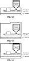
- a pre-metal dielectric layer e.g. a silicon oxide layer is deposited onto the entire area covering all the structures obtained in previous steps. The latter is shown in FIG. 13 .
- the pre-metal dielectric layer of the previous step is planarized, e.g. by chemical-mechanical polishing, and etched back to the level of the top surface of the nanoridge III-V passivation layer. The latter is shown in FIG. 14 .
- the top III-V passivation layer of the active direct bandgap III-V material nanoridge waveguide is removed, e.g. through etching, as shown in FIG. 15 .
- the one or more p-doped III-V material layers of the ninth step are selectively etched to form narrow top contact fins to the active III-V material nanoridge waveguides.
- the top contact fins may have widths of 20 nm to 100 nm.
- an additional top passivation layer may be applied to the current material stack. The latter is shown in FIG. 16 and FIG. 17 .
- a pre-metal dielectric layer is deposited on top of the current material stack, followed by a planarization process.
- metal interconnects e.g. copper damascene pads
- metal interconnects are provided to the material stack in regions where said contact plugs exist, by first selectively patterning an underlying insulating oxide layer, then applying an overfilling metallization layer, and finally removing the excess metal by planarization, e.g. chemical-mechanical planarization.
- planarization e.g. chemical-mechanical planarization. The latter is illustrated in FIG. 19 .
- FIG. 20 A simulation was performed comparing the III-V semiconductor nanoridge waveguide with a top electrode as known from prior art and a III-V semiconductor nanoridge waveguide with an upper electrode wrapping around the freestanding wide body portion.
- the corresponding band diagram is shown in FIG. 20 .
- FIG 21 the carrier profile under forward bias is shown, both for the case of a top electrode only (according to prior art) and a wrapping around electrode. It can be seen that an injection efficiency is obtained which is up to twice as high for a wrapping around electrode compared to the top electrode only. Furthermore, it could be noted that a more uniform injection is obtained across the multi quantum wells.
Landscapes
- Physics & Mathematics (AREA)
- Nonlinear Science (AREA)
- General Physics & Mathematics (AREA)
- Optics & Photonics (AREA)
- Engineering & Computer Science (AREA)
- Microelectronics & Electronic Packaging (AREA)
- Optical Integrated Circuits (AREA)
- Optical Modulation, Optical Deflection, Nonlinear Optics, Optical Demodulation, Optical Logic Elements (AREA)
Priority Applications (2)
| Application Number | Priority Date | Filing Date | Title |
|---|---|---|---|
| EP17211015.7A EP3506000B1 (fr) | 2017-12-29 | 2017-12-29 | Structure de guide d'onde semi-conducteur iii-v nanoridge |
| US16/228,486 US10690852B2 (en) | 2017-12-29 | 2018-12-20 | III-V semiconductor waveguide nanoridge structure |
Applications Claiming Priority (1)
| Application Number | Priority Date | Filing Date | Title |
|---|---|---|---|
| EP17211015.7A EP3506000B1 (fr) | 2017-12-29 | 2017-12-29 | Structure de guide d'onde semi-conducteur iii-v nanoridge |
Publications (2)
| Publication Number | Publication Date |
|---|---|
| EP3506000A1 true EP3506000A1 (fr) | 2019-07-03 |
| EP3506000B1 EP3506000B1 (fr) | 2020-10-07 |
Family
ID=60856927
Family Applications (1)
| Application Number | Title | Priority Date | Filing Date |
|---|---|---|---|
| EP17211015.7A Active EP3506000B1 (fr) | 2017-12-29 | 2017-12-29 | Structure de guide d'onde semi-conducteur iii-v nanoridge |
Country Status (2)
| Country | Link |
|---|---|
| US (1) | US10690852B2 (fr) |
| EP (1) | EP3506000B1 (fr) |
Cited By (2)
| Publication number | Priority date | Publication date | Assignee | Title |
|---|---|---|---|---|
| WO2021105138A1 (fr) * | 2019-11-26 | 2021-06-03 | Rockley Photonics Limited | Dispositif optoélectronique à semi-conducteur iii-v/silicium intégré et son procédé de fabrication |
| EP3936930A1 (fr) * | 2020-07-08 | 2022-01-12 | Imec VZW | Modulateur de phase opto-électronique monolithique iii-v-sur-silicium comportant un guide d'onde à nervure |
Families Citing this family (2)
| Publication number | Priority date | Publication date | Assignee | Title |
|---|---|---|---|---|
| EP3467973A1 (fr) * | 2017-10-04 | 2019-04-10 | IMEC vzw | Système photonique à guide d'onde actif-passif |
| CN111126609B (zh) * | 2019-12-20 | 2021-04-23 | 深圳前海微众银行股份有限公司 | 基于联邦学习的知识迁移方法、装置、设备及介质 |
Citations (6)
| Publication number | Priority date | Publication date | Assignee | Title |
|---|---|---|---|---|
| US20040218259A1 (en) * | 2003-02-21 | 2004-11-04 | Rongqing Hui | Method and apparatus for use of III-nitride wide bandgap semiconductors in optical communications |
| US20040258344A1 (en) * | 2003-06-19 | 2004-12-23 | Behzad Fardi | Thermally isolating optical devices |
| JP2006235379A (ja) * | 2005-02-25 | 2006-09-07 | Nippon Telegr & Teleph Corp <Ntt> | 熱光学位相変調器及びその製造方法 |
| EP2015116A2 (fr) * | 2007-07-12 | 2009-01-14 | NEC Corporation | Structure de silicium, en particulier comprenant un guide d'onde optique, et son procédé de fabrication |
| EP2985645A1 (fr) * | 2014-08-13 | 2016-02-17 | Huawei Technologies Co., Ltd. | Procédé de production d'un circuit optique intégré et circuit correspondant |
| US20160087160A1 (en) * | 2014-09-22 | 2016-03-24 | International Business Machines Corporation | Iii-v photonic integrated circuits on silicon substrate |
Family Cites Families (10)
| Publication number | Priority date | Publication date | Assignee | Title |
|---|---|---|---|---|
| DE3788527T2 (de) * | 1986-04-01 | 1994-05-11 | Matsushita Electric Ind Co Ltd | Bipolarer Transistor und sein Herstellungsverfahren. |
| US4749441A (en) * | 1986-12-11 | 1988-06-07 | General Motors Corporation | Semiconductor mushroom structure fabrication |
| JPH0997946A (ja) * | 1995-07-21 | 1997-04-08 | Matsushita Electric Ind Co Ltd | 半導体レーザ及びその製造方法 |
| JP4828018B2 (ja) * | 2000-11-06 | 2011-11-30 | 三菱電機株式会社 | 光変調器およびその製造方法並びに光半導体装置 |
| US7072557B2 (en) * | 2001-12-21 | 2006-07-04 | Infinera Corporation | InP-based photonic integrated circuits with Al-containing waveguide cores and InP-based array waveguide gratings (AWGs) and avalanche photodiodes (APDs) and other optical components containing an InAlGaAs waveguide core |
| US8502263B2 (en) * | 2006-10-19 | 2013-08-06 | Taiwan Semiconductor Manufacturing Company, Ltd. | Light-emitter-based devices with lattice-mismatched semiconductor structures |
| JP5186776B2 (ja) * | 2007-02-22 | 2013-04-24 | 富士通株式会社 | 半導体装置及びその製造方法 |
| CN102160145B (zh) * | 2008-09-19 | 2013-08-21 | 台湾积体电路制造股份有限公司 | 通过外延层过成长的元件形成 |
| KR101582623B1 (ko) * | 2011-12-30 | 2016-01-05 | 서울대학교산학협력단 | 실리콘 기판에 집적 가능한 화합물 터널링 전계효과 트랜지스터 및 그 제조방법 |
| JP7218082B2 (ja) * | 2016-09-26 | 2023-02-06 | 日本ルメンタム株式会社 | 光半導体素子、光モジュール及び光半導体素子の製造方法 |
-
2017
- 2017-12-29 EP EP17211015.7A patent/EP3506000B1/fr active Active
-
2018
- 2018-12-20 US US16/228,486 patent/US10690852B2/en active Active
Patent Citations (6)
| Publication number | Priority date | Publication date | Assignee | Title |
|---|---|---|---|---|
| US20040218259A1 (en) * | 2003-02-21 | 2004-11-04 | Rongqing Hui | Method and apparatus for use of III-nitride wide bandgap semiconductors in optical communications |
| US20040258344A1 (en) * | 2003-06-19 | 2004-12-23 | Behzad Fardi | Thermally isolating optical devices |
| JP2006235379A (ja) * | 2005-02-25 | 2006-09-07 | Nippon Telegr & Teleph Corp <Ntt> | 熱光学位相変調器及びその製造方法 |
| EP2015116A2 (fr) * | 2007-07-12 | 2009-01-14 | NEC Corporation | Structure de silicium, en particulier comprenant un guide d'onde optique, et son procédé de fabrication |
| EP2985645A1 (fr) * | 2014-08-13 | 2016-02-17 | Huawei Technologies Co., Ltd. | Procédé de production d'un circuit optique intégré et circuit correspondant |
| US20160087160A1 (en) * | 2014-09-22 | 2016-03-24 | International Business Machines Corporation | Iii-v photonic integrated circuits on silicon substrate |
Cited By (3)
| Publication number | Priority date | Publication date | Assignee | Title |
|---|---|---|---|---|
| WO2021105138A1 (fr) * | 2019-11-26 | 2021-06-03 | Rockley Photonics Limited | Dispositif optoélectronique à semi-conducteur iii-v/silicium intégré et son procédé de fabrication |
| EP3936930A1 (fr) * | 2020-07-08 | 2022-01-12 | Imec VZW | Modulateur de phase opto-électronique monolithique iii-v-sur-silicium comportant un guide d'onde à nervure |
| US11556043B2 (en) | 2020-07-08 | 2023-01-17 | Imec Vzw | Monolithic III-V-on-silicon opto-electronic phase modulator with a ridge waveguide |
Also Published As
| Publication number | Publication date |
|---|---|
| US20190219846A1 (en) | 2019-07-18 |
| EP3506000B1 (fr) | 2020-10-07 |
| US10690852B2 (en) | 2020-06-23 |
Similar Documents
| Publication | Publication Date | Title |
|---|---|---|
| US10690852B2 (en) | III-V semiconductor waveguide nanoridge structure | |
| US9413139B2 (en) | Hybrid waveguide lasers and methods for fabricating hybrid waveguide lasers | |
| US10468551B2 (en) | Light-emitter-based devices with lattice-mismatched semiconductor structures | |
| US8741684B2 (en) | Co-integration of photonic devices on a silicon photonics platform | |
| US9823414B2 (en) | Method for fabricating a semiconductor device for use in an optical application | |
| US11029466B2 (en) | Photonics structure with integrated laser | |
| Shi et al. | 1.55-μm lasers epitaxially grown on silicon | |
| US9368579B2 (en) | Selective area growth of germanium and silicon-germanium in silicon waveguides for on-chip optical interconnect applications | |
| CN111769437B (zh) | 布拉格光栅及其制备方法、分布反馈激光器 | |
| EP3471221B1 (fr) | Système photonique à guide d'onde actif-passif | |
| US10763643B2 (en) | Laser devices | |
| Shang et al. | Low-threshold epitaxially grown 1.3-μm InAs quantum dot lasers on patterned (001) Si | |
| CN111628410A (zh) | 一种1.55微米波长硅基量子点激光器外延材料及制备方法 | |
| EP4205184A1 (fr) | Diode dotée d'une région intrinsèque sensible à la lumière | |
| US20200259312A1 (en) | Plasmonic laser | |
| CN109478764B (zh) | 基于异质结构的集成光子装置、方法和应用 | |
| US10944235B2 (en) | Method for producing a light source and light source | |
| CN103794985A (zh) | 半导体装置及其制造方法 | |
| US10389090B2 (en) | Lateral growth of edge-emitting lasers | |
| US20230244029A1 (en) | Photonics optoelectrical system | |
| CN115347450A (zh) | 一种iii-v族化合物半导体光芯片与硅基电芯片实现晶圆级别集成的方法 | |
| Yu-Dong et al. | Fabrication of monolithic integration of 1.55/spl mu/m QW laser and HBT |
Legal Events
| Date | Code | Title | Description |
|---|---|---|---|
| PUAI | Public reference made under article 153(3) epc to a published international application that has entered the european phase |
Free format text: ORIGINAL CODE: 0009012 |
|
| STAA | Information on the status of an ep patent application or granted ep patent |
Free format text: STATUS: THE APPLICATION HAS BEEN PUBLISHED |
|
| AK | Designated contracting states |
Kind code of ref document: A1 Designated state(s): AL AT BE BG CH CY CZ DE DK EE ES FI FR GB GR HR HU IE IS IT LI LT LU LV MC MK MT NL NO PL PT RO RS SE SI SK SM TR |
|
| AX | Request for extension of the european patent |
Extension state: BA ME |
|
| STAA | Information on the status of an ep patent application or granted ep patent |
Free format text: STATUS: REQUEST FOR EXAMINATION WAS MADE |
|
| 17P | Request for examination filed |
Effective date: 20191220 |
|
| RBV | Designated contracting states (corrected) |
Designated state(s): AL AT BE BG CH CY CZ DE DK EE ES FI FR GB GR HR HU IE IS IT LI LT LU LV MC MK MT NL NO PL PT RO RS SE SI SK SM TR |
|
| RIC1 | Information provided on ipc code assigned before grant |
Ipc: G02B 6/12 20060101ALN20200528BHEP Ipc: G02B 6/13 20060101ALI20200528BHEP Ipc: G02F 1/025 20060101ALI20200528BHEP Ipc: G02F 1/017 20060101AFI20200528BHEP Ipc: G02F 1/225 20060101ALI20200528BHEP |
|
| GRAP | Despatch of communication of intention to grant a patent |
Free format text: ORIGINAL CODE: EPIDOSNIGR1 |
|
| STAA | Information on the status of an ep patent application or granted ep patent |
Free format text: STATUS: GRANT OF PATENT IS INTENDED |
|
| RIC1 | Information provided on ipc code assigned before grant |
Ipc: G02F 1/225 20060101ALI20200610BHEP Ipc: G02F 1/017 20060101AFI20200610BHEP Ipc: G02F 1/025 20060101ALI20200610BHEP Ipc: G02B 6/13 20060101ALI20200610BHEP Ipc: G02B 6/12 20060101ALN20200610BHEP |
|
| INTG | Intention to grant announced |
Effective date: 20200706 |
|
| GRAS | Grant fee paid |
Free format text: ORIGINAL CODE: EPIDOSNIGR3 |
|
| GRAA | (expected) grant |
Free format text: ORIGINAL CODE: 0009210 |
|
| STAA | Information on the status of an ep patent application or granted ep patent |
Free format text: STATUS: THE PATENT HAS BEEN GRANTED |
|
| AK | Designated contracting states |
Kind code of ref document: B1 Designated state(s): AL AT BE BG CH CY CZ DE DK EE ES FI FR GB GR HR HU IE IS IT LI LT LU LV MC MK MT NL NO PL PT RO RS SE SI SK SM TR |
|
| REG | Reference to a national code |
Ref country code: GB Ref legal event code: FG4D |
|
| REG | Reference to a national code |
Ref country code: AT Ref legal event code: REF Ref document number: 1321779 Country of ref document: AT Kind code of ref document: T Effective date: 20201015 Ref country code: CH Ref legal event code: EP |
|
| REG | Reference to a national code |
Ref country code: IE Ref legal event code: FG4D |
|
| REG | Reference to a national code |
Ref country code: DE Ref legal event code: R096 Ref document number: 602017024952 Country of ref document: DE |
|
| REG | Reference to a national code |
Ref country code: NL Ref legal event code: MP Effective date: 20201007 |
|
| REG | Reference to a national code |
Ref country code: AT Ref legal event code: MK05 Ref document number: 1321779 Country of ref document: AT Kind code of ref document: T Effective date: 20201007 |
|
| PG25 | Lapsed in a contracting state [announced via postgrant information from national office to epo] |
Ref country code: RS Free format text: LAPSE BECAUSE OF FAILURE TO SUBMIT A TRANSLATION OF THE DESCRIPTION OR TO PAY THE FEE WITHIN THE PRESCRIBED TIME-LIMIT Effective date: 20201007 Ref country code: PT Free format text: LAPSE BECAUSE OF FAILURE TO SUBMIT A TRANSLATION OF THE DESCRIPTION OR TO PAY THE FEE WITHIN THE PRESCRIBED TIME-LIMIT Effective date: 20210208 Ref country code: NO Free format text: LAPSE BECAUSE OF FAILURE TO SUBMIT A TRANSLATION OF THE DESCRIPTION OR TO PAY THE FEE WITHIN THE PRESCRIBED TIME-LIMIT Effective date: 20210107 Ref country code: FI Free format text: LAPSE BECAUSE OF FAILURE TO SUBMIT A TRANSLATION OF THE DESCRIPTION OR TO PAY THE FEE WITHIN THE PRESCRIBED TIME-LIMIT Effective date: 20201007 Ref country code: GR Free format text: LAPSE BECAUSE OF FAILURE TO SUBMIT A TRANSLATION OF THE DESCRIPTION OR TO PAY THE FEE WITHIN THE PRESCRIBED TIME-LIMIT Effective date: 20210108 |
|
| REG | Reference to a national code |
Ref country code: LT Ref legal event code: MG4D |
|
| PG25 | Lapsed in a contracting state [announced via postgrant information from national office to epo] |
Ref country code: SE Free format text: LAPSE BECAUSE OF FAILURE TO SUBMIT A TRANSLATION OF THE DESCRIPTION OR TO PAY THE FEE WITHIN THE PRESCRIBED TIME-LIMIT Effective date: 20201007 Ref country code: ES Free format text: LAPSE BECAUSE OF FAILURE TO SUBMIT A TRANSLATION OF THE DESCRIPTION OR TO PAY THE FEE WITHIN THE PRESCRIBED TIME-LIMIT Effective date: 20201007 Ref country code: AT Free format text: LAPSE BECAUSE OF FAILURE TO SUBMIT A TRANSLATION OF THE DESCRIPTION OR TO PAY THE FEE WITHIN THE PRESCRIBED TIME-LIMIT Effective date: 20201007 Ref country code: BG Free format text: LAPSE BECAUSE OF FAILURE TO SUBMIT A TRANSLATION OF THE DESCRIPTION OR TO PAY THE FEE WITHIN THE PRESCRIBED TIME-LIMIT Effective date: 20210107 Ref country code: PL Free format text: LAPSE BECAUSE OF FAILURE TO SUBMIT A TRANSLATION OF THE DESCRIPTION OR TO PAY THE FEE WITHIN THE PRESCRIBED TIME-LIMIT Effective date: 20201007 Ref country code: IS Free format text: LAPSE BECAUSE OF FAILURE TO SUBMIT A TRANSLATION OF THE DESCRIPTION OR TO PAY THE FEE WITHIN THE PRESCRIBED TIME-LIMIT Effective date: 20210207 Ref country code: LV Free format text: LAPSE BECAUSE OF FAILURE TO SUBMIT A TRANSLATION OF THE DESCRIPTION OR TO PAY THE FEE WITHIN THE PRESCRIBED TIME-LIMIT Effective date: 20201007 |
|
| PG25 | Lapsed in a contracting state [announced via postgrant information from national office to epo] |
Ref country code: HR Free format text: LAPSE BECAUSE OF FAILURE TO SUBMIT A TRANSLATION OF THE DESCRIPTION OR TO PAY THE FEE WITHIN THE PRESCRIBED TIME-LIMIT Effective date: 20201007 Ref country code: NL Free format text: LAPSE BECAUSE OF FAILURE TO SUBMIT A TRANSLATION OF THE DESCRIPTION OR TO PAY THE FEE WITHIN THE PRESCRIBED TIME-LIMIT Effective date: 20201007 |
|
| REG | Reference to a national code |
Ref country code: DE Ref legal event code: R097 Ref document number: 602017024952 Country of ref document: DE |
|
| PG25 | Lapsed in a contracting state [announced via postgrant information from national office to epo] |
Ref country code: LT Free format text: LAPSE BECAUSE OF FAILURE TO SUBMIT A TRANSLATION OF THE DESCRIPTION OR TO PAY THE FEE WITHIN THE PRESCRIBED TIME-LIMIT Effective date: 20201007 Ref country code: CZ Free format text: LAPSE BECAUSE OF FAILURE TO SUBMIT A TRANSLATION OF THE DESCRIPTION OR TO PAY THE FEE WITHIN THE PRESCRIBED TIME-LIMIT Effective date: 20201007 Ref country code: EE Free format text: LAPSE BECAUSE OF FAILURE TO SUBMIT A TRANSLATION OF THE DESCRIPTION OR TO PAY THE FEE WITHIN THE PRESCRIBED TIME-LIMIT Effective date: 20201007 Ref country code: SM Free format text: LAPSE BECAUSE OF FAILURE TO SUBMIT A TRANSLATION OF THE DESCRIPTION OR TO PAY THE FEE WITHIN THE PRESCRIBED TIME-LIMIT Effective date: 20201007 Ref country code: SK Free format text: LAPSE BECAUSE OF FAILURE TO SUBMIT A TRANSLATION OF THE DESCRIPTION OR TO PAY THE FEE WITHIN THE PRESCRIBED TIME-LIMIT Effective date: 20201007 Ref country code: RO Free format text: LAPSE BECAUSE OF FAILURE TO SUBMIT A TRANSLATION OF THE DESCRIPTION OR TO PAY THE FEE WITHIN THE PRESCRIBED TIME-LIMIT Effective date: 20201007 |
|
| REG | Reference to a national code |
Ref country code: CH Ref legal event code: PL |
|
| PLBE | No opposition filed within time limit |
Free format text: ORIGINAL CODE: 0009261 |
|
| STAA | Information on the status of an ep patent application or granted ep patent |
Free format text: STATUS: NO OPPOSITION FILED WITHIN TIME LIMIT |
|
| PG25 | Lapsed in a contracting state [announced via postgrant information from national office to epo] |
Ref country code: MC Free format text: LAPSE BECAUSE OF FAILURE TO SUBMIT A TRANSLATION OF THE DESCRIPTION OR TO PAY THE FEE WITHIN THE PRESCRIBED TIME-LIMIT Effective date: 20201007 Ref country code: DK Free format text: LAPSE BECAUSE OF FAILURE TO SUBMIT A TRANSLATION OF THE DESCRIPTION OR TO PAY THE FEE WITHIN THE PRESCRIBED TIME-LIMIT Effective date: 20201007 |
|
| REG | Reference to a national code |
Ref country code: BE Ref legal event code: MM Effective date: 20201231 |
|
| 26N | No opposition filed |
Effective date: 20210708 |
|
| PG25 | Lapsed in a contracting state [announced via postgrant information from national office to epo] |
Ref country code: LU Free format text: LAPSE BECAUSE OF NON-PAYMENT OF DUE FEES Effective date: 20201229 Ref country code: IT Free format text: LAPSE BECAUSE OF FAILURE TO SUBMIT A TRANSLATION OF THE DESCRIPTION OR TO PAY THE FEE WITHIN THE PRESCRIBED TIME-LIMIT Effective date: 20201007 Ref country code: FR Free format text: LAPSE BECAUSE OF NON-PAYMENT OF DUE FEES Effective date: 20201231 Ref country code: AL Free format text: LAPSE BECAUSE OF FAILURE TO SUBMIT A TRANSLATION OF THE DESCRIPTION OR TO PAY THE FEE WITHIN THE PRESCRIBED TIME-LIMIT Effective date: 20201007 Ref country code: IE Free format text: LAPSE BECAUSE OF NON-PAYMENT OF DUE FEES Effective date: 20201229 |
|
| PG25 | Lapsed in a contracting state [announced via postgrant information from national office to epo] |
Ref country code: LI Free format text: LAPSE BECAUSE OF NON-PAYMENT OF DUE FEES Effective date: 20201231 Ref country code: CH Free format text: LAPSE BECAUSE OF NON-PAYMENT OF DUE FEES Effective date: 20201231 Ref country code: SI Free format text: LAPSE BECAUSE OF FAILURE TO SUBMIT A TRANSLATION OF THE DESCRIPTION OR TO PAY THE FEE WITHIN THE PRESCRIBED TIME-LIMIT Effective date: 20201007 |
|
| PG25 | Lapsed in a contracting state [announced via postgrant information from national office to epo] |
Ref country code: IS Free format text: LAPSE BECAUSE OF FAILURE TO SUBMIT A TRANSLATION OF THE DESCRIPTION OR TO PAY THE FEE WITHIN THE PRESCRIBED TIME-LIMIT Effective date: 20210207 Ref country code: TR Free format text: LAPSE BECAUSE OF FAILURE TO SUBMIT A TRANSLATION OF THE DESCRIPTION OR TO PAY THE FEE WITHIN THE PRESCRIBED TIME-LIMIT Effective date: 20201007 Ref country code: MT Free format text: LAPSE BECAUSE OF FAILURE TO SUBMIT A TRANSLATION OF THE DESCRIPTION OR TO PAY THE FEE WITHIN THE PRESCRIBED TIME-LIMIT Effective date: 20201007 Ref country code: CY Free format text: LAPSE BECAUSE OF FAILURE TO SUBMIT A TRANSLATION OF THE DESCRIPTION OR TO PAY THE FEE WITHIN THE PRESCRIBED TIME-LIMIT Effective date: 20201007 |
|
| PG25 | Lapsed in a contracting state [announced via postgrant information from national office to epo] |
Ref country code: MK Free format text: LAPSE BECAUSE OF FAILURE TO SUBMIT A TRANSLATION OF THE DESCRIPTION OR TO PAY THE FEE WITHIN THE PRESCRIBED TIME-LIMIT Effective date: 20201007 |
|
| PG25 | Lapsed in a contracting state [announced via postgrant information from national office to epo] |
Ref country code: BE Free format text: LAPSE BECAUSE OF NON-PAYMENT OF DUE FEES Effective date: 20201231 |
|
| GBPC | Gb: european patent ceased through non-payment of renewal fee |
Effective date: 20211229 |
|
| PG25 | Lapsed in a contracting state [announced via postgrant information from national office to epo] |
Ref country code: GB Free format text: LAPSE BECAUSE OF NON-PAYMENT OF DUE FEES Effective date: 20211229 |
|
| P01 | Opt-out of the competence of the unified patent court (upc) registered |
Effective date: 20230513 |
|
| PGFP | Annual fee paid to national office [announced via postgrant information from national office to epo] |
Ref country code: DE Payment date: 20231121 Year of fee payment: 7 |