EP3503367A1 - Switched capacitor converter with compensation inductor - Google Patents
Switched capacitor converter with compensation inductor Download PDFInfo
- Publication number
- EP3503367A1 EP3503367A1 EP18213802.4A EP18213802A EP3503367A1 EP 3503367 A1 EP3503367 A1 EP 3503367A1 EP 18213802 A EP18213802 A EP 18213802A EP 3503367 A1 EP3503367 A1 EP 3503367A1
- Authority
- EP
- European Patent Office
- Prior art keywords
- switch
- resonant
- capacitor
- rectifier
- switched
- Prior art date
- Legal status (The legal status is an assumption and is not a legal conclusion. Google has not performed a legal analysis and makes no representation as to the accuracy of the status listed.)
- Granted
Links
Images





Classifications
-
- H—ELECTRICITY
- H02—GENERATION; CONVERSION OR DISTRIBUTION OF ELECTRIC POWER
- H02M—APPARATUS FOR CONVERSION BETWEEN AC AND AC, BETWEEN AC AND DC, OR BETWEEN DC AND DC, AND FOR USE WITH MAINS OR SIMILAR POWER SUPPLY SYSTEMS; CONVERSION OF DC OR AC INPUT POWER INTO SURGE OUTPUT POWER; CONTROL OR REGULATION THEREOF
- H02M1/00—Details of apparatus for conversion
- H02M1/08—Circuits specially adapted for the generation of control voltages for semiconductor devices incorporated in static converters
- H02M1/083—Circuits specially adapted for the generation of control voltages for semiconductor devices incorporated in static converters for the ignition at the zero crossing of the voltage or the current
-
- H—ELECTRICITY
- H02—GENERATION; CONVERSION OR DISTRIBUTION OF ELECTRIC POWER
- H02M—APPARATUS FOR CONVERSION BETWEEN AC AND AC, BETWEEN AC AND DC, OR BETWEEN DC AND DC, AND FOR USE WITH MAINS OR SIMILAR POWER SUPPLY SYSTEMS; CONVERSION OF DC OR AC INPUT POWER INTO SURGE OUTPUT POWER; CONTROL OR REGULATION THEREOF
- H02M1/00—Details of apparatus for conversion
- H02M1/14—Arrangements for reducing ripples from DC input or output
- H02M1/15—Arrangements for reducing ripples from DC input or output using active elements
-
- H—ELECTRICITY
- H02—GENERATION; CONVERSION OR DISTRIBUTION OF ELECTRIC POWER
- H02M—APPARATUS FOR CONVERSION BETWEEN AC AND AC, BETWEEN AC AND DC, OR BETWEEN DC AND DC, AND FOR USE WITH MAINS OR SIMILAR POWER SUPPLY SYSTEMS; CONVERSION OF DC OR AC INPUT POWER INTO SURGE OUTPUT POWER; CONTROL OR REGULATION THEREOF
- H02M1/00—Details of apparatus for conversion
- H02M1/0048—Circuits or arrangements for reducing losses
- H02M1/0054—Transistor switching losses
- H02M1/0058—Transistor switching losses by employing soft switching techniques, i.e. commutation of transistors when applied voltage is zero or when current flow is zero
-
- H—ELECTRICITY
- H02—GENERATION; CONVERSION OR DISTRIBUTION OF ELECTRIC POWER
- H02M—APPARATUS FOR CONVERSION BETWEEN AC AND AC, BETWEEN AC AND DC, OR BETWEEN DC AND DC, AND FOR USE WITH MAINS OR SIMILAR POWER SUPPLY SYSTEMS; CONVERSION OF DC OR AC INPUT POWER INTO SURGE OUTPUT POWER; CONTROL OR REGULATION THEREOF
- H02M3/00—Conversion of DC power input into DC power output
- H02M3/02—Conversion of DC power input into DC power output without intermediate conversion into AC
- H02M3/04—Conversion of DC power input into DC power output without intermediate conversion into AC by static converters
- H02M3/06—Conversion of DC power input into DC power output without intermediate conversion into AC by static converters using resistors or capacitors, e.g. potential divider
- H02M3/07—Conversion of DC power input into DC power output without intermediate conversion into AC by static converters using resistors or capacitors, e.g. potential divider using capacitors charged and discharged alternately by semiconductor devices with control electrode, e.g. charge pumps
-
- H—ELECTRICITY
- H02—GENERATION; CONVERSION OR DISTRIBUTION OF ELECTRIC POWER
- H02M—APPARATUS FOR CONVERSION BETWEEN AC AND AC, BETWEEN AC AND DC, OR BETWEEN DC AND DC, AND FOR USE WITH MAINS OR SIMILAR POWER SUPPLY SYSTEMS; CONVERSION OF DC OR AC INPUT POWER INTO SURGE OUTPUT POWER; CONTROL OR REGULATION THEREOF
- H02M3/00—Conversion of DC power input into DC power output
- H02M3/02—Conversion of DC power input into DC power output without intermediate conversion into AC
- H02M3/04—Conversion of DC power input into DC power output without intermediate conversion into AC by static converters
- H02M3/10—Conversion of DC power input into DC power output without intermediate conversion into AC by static converters using discharge tubes with control electrode or semiconductor devices with control electrode
- H02M3/145—Conversion of DC power input into DC power output without intermediate conversion into AC by static converters using discharge tubes with control electrode or semiconductor devices with control electrode using devices of a triode or transistor type requiring continuous application of a control signal
- H02M3/155—Conversion of DC power input into DC power output without intermediate conversion into AC by static converters using discharge tubes with control electrode or semiconductor devices with control electrode using devices of a triode or transistor type requiring continuous application of a control signal using semiconductor devices only
- H02M3/156—Conversion of DC power input into DC power output without intermediate conversion into AC by static converters using discharge tubes with control electrode or semiconductor devices with control electrode using devices of a triode or transistor type requiring continuous application of a control signal using semiconductor devices only with automatic control of output voltage or current, e.g. switching regulators
- H02M3/158—Conversion of DC power input into DC power output without intermediate conversion into AC by static converters using discharge tubes with control electrode or semiconductor devices with control electrode using devices of a triode or transistor type requiring continuous application of a control signal using semiconductor devices only with automatic control of output voltage or current, e.g. switching regulators including plural semiconductor devices as final control devices for a single load
-
- H—ELECTRICITY
- H02—GENERATION; CONVERSION OR DISTRIBUTION OF ELECTRIC POWER
- H02M—APPARATUS FOR CONVERSION BETWEEN AC AND AC, BETWEEN AC AND DC, OR BETWEEN DC AND DC, AND FOR USE WITH MAINS OR SIMILAR POWER SUPPLY SYSTEMS; CONVERSION OF DC OR AC INPUT POWER INTO SURGE OUTPUT POWER; CONTROL OR REGULATION THEREOF
- H02M3/00—Conversion of DC power input into DC power output
- H02M3/02—Conversion of DC power input into DC power output without intermediate conversion into AC
- H02M3/04—Conversion of DC power input into DC power output without intermediate conversion into AC by static converters
- H02M3/10—Conversion of DC power input into DC power output without intermediate conversion into AC by static converters using discharge tubes with control electrode or semiconductor devices with control electrode
- H02M3/145—Conversion of DC power input into DC power output without intermediate conversion into AC by static converters using discharge tubes with control electrode or semiconductor devices with control electrode using devices of a triode or transistor type requiring continuous application of a control signal
- H02M3/155—Conversion of DC power input into DC power output without intermediate conversion into AC by static converters using discharge tubes with control electrode or semiconductor devices with control electrode using devices of a triode or transistor type requiring continuous application of a control signal using semiconductor devices only
- H02M3/156—Conversion of DC power input into DC power output without intermediate conversion into AC by static converters using discharge tubes with control electrode or semiconductor devices with control electrode using devices of a triode or transistor type requiring continuous application of a control signal using semiconductor devices only with automatic control of output voltage or current, e.g. switching regulators
- H02M3/158—Conversion of DC power input into DC power output without intermediate conversion into AC by static converters using discharge tubes with control electrode or semiconductor devices with control electrode using devices of a triode or transistor type requiring continuous application of a control signal using semiconductor devices only with automatic control of output voltage or current, e.g. switching regulators including plural semiconductor devices as final control devices for a single load
- H02M3/1588—Conversion of DC power input into DC power output without intermediate conversion into AC by static converters using discharge tubes with control electrode or semiconductor devices with control electrode using devices of a triode or transistor type requiring continuous application of a control signal using semiconductor devices only with automatic control of output voltage or current, e.g. switching regulators including plural semiconductor devices as final control devices for a single load comprising at least one synchronous rectifier element
-
- H—ELECTRICITY
- H02—GENERATION; CONVERSION OR DISTRIBUTION OF ELECTRIC POWER
- H02M—APPARATUS FOR CONVERSION BETWEEN AC AND AC, BETWEEN AC AND DC, OR BETWEEN DC AND DC, AND FOR USE WITH MAINS OR SIMILAR POWER SUPPLY SYSTEMS; CONVERSION OF DC OR AC INPUT POWER INTO SURGE OUTPUT POWER; CONTROL OR REGULATION THEREOF
- H02M3/00—Conversion of DC power input into DC power output
- H02M3/22—Conversion of DC power input into DC power output with intermediate conversion into AC
- H02M3/24—Conversion of DC power input into DC power output with intermediate conversion into AC by static converters
- H02M3/28—Conversion of DC power input into DC power output with intermediate conversion into AC by static converters using discharge tubes with control electrode or semiconductor devices with control electrode to produce the intermediate AC
- H02M3/325—Conversion of DC power input into DC power output with intermediate conversion into AC by static converters using discharge tubes with control electrode or semiconductor devices with control electrode to produce the intermediate AC using devices of a triode or a transistor type requiring continuous application of a control signal
- H02M3/335—Conversion of DC power input into DC power output with intermediate conversion into AC by static converters using discharge tubes with control electrode or semiconductor devices with control electrode to produce the intermediate AC using devices of a triode or a transistor type requiring continuous application of a control signal using semiconductor devices only
-
- H—ELECTRICITY
- H03—ELECTRONIC CIRCUITRY
- H03H—IMPEDANCE NETWORKS, e.g. RESONANT CIRCUITS; RESONATORS
- H03H19/00—Networks using time-varying elements, e.g. N-path filters
- H03H19/002—N-path filters
-
- H—ELECTRICITY
- H02—GENERATION; CONVERSION OR DISTRIBUTION OF ELECTRIC POWER
- H02M—APPARATUS FOR CONVERSION BETWEEN AC AND AC, BETWEEN AC AND DC, OR BETWEEN DC AND DC, AND FOR USE WITH MAINS OR SIMILAR POWER SUPPLY SYSTEMS; CONVERSION OF DC OR AC INPUT POWER INTO SURGE OUTPUT POWER; CONTROL OR REGULATION THEREOF
- H02M1/00—Details of apparatus for conversion
- H02M1/0067—Converter structures employing plural converter units, other than for parallel operation of the units on a single load
- H02M1/007—Plural converter units in cascade
-
- H—ELECTRICITY
- H02—GENERATION; CONVERSION OR DISTRIBUTION OF ELECTRIC POWER
- H02M—APPARATUS FOR CONVERSION BETWEEN AC AND AC, BETWEEN AC AND DC, OR BETWEEN DC AND DC, AND FOR USE WITH MAINS OR SIMILAR POWER SUPPLY SYSTEMS; CONVERSION OF DC OR AC INPUT POWER INTO SURGE OUTPUT POWER; CONTROL OR REGULATION THEREOF
- H02M1/00—Details of apparatus for conversion
- H02M1/0067—Converter structures employing plural converter units, other than for parallel operation of the units on a single load
- H02M1/0077—Plural converter units whose outputs are connected in series
-
- Y—GENERAL TAGGING OF NEW TECHNOLOGICAL DEVELOPMENTS; GENERAL TAGGING OF CROSS-SECTIONAL TECHNOLOGIES SPANNING OVER SEVERAL SECTIONS OF THE IPC; TECHNICAL SUBJECTS COVERED BY FORMER USPC CROSS-REFERENCE ART COLLECTIONS [XRACs] AND DIGESTS
- Y02—TECHNOLOGIES OR APPLICATIONS FOR MITIGATION OR ADAPTATION AGAINST CLIMATE CHANGE
- Y02B—CLIMATE CHANGE MITIGATION TECHNOLOGIES RELATED TO BUILDINGS, e.g. HOUSING, HOUSE APPLIANCES OR RELATED END-USER APPLICATIONS
- Y02B70/00—Technologies for an efficient end-user side electric power management and consumption
- Y02B70/10—Technologies improving the efficiency by using switched-mode power supplies [SMPS], i.e. efficient power electronics conversion e.g. power factor correction or reduction of losses in power supplies or efficient standby modes
Definitions
- 12V DC bus For supplying power to a variety of circuits.
- a 12V DC bus may be widely distributed within a system and typically is down-converted to a lower voltage, e.g., 3.3V, 1.8V, 1.2V, for use by loads requiring lower voltage levels.
- Such down-conversion is preferably performed at the point-of-load (POL), so that the voltage level required by the load may be more efficiently regulated.
- POL point-of-load
- Matching the switching frequency of the STC to the resonant frequency of one or more resonant tanks within the STC presents practical challenges beyond the challenges associated with conventional resonant switching converters that are not based on a switched-capacitor topology.
- Such conventional resonant converters may characterize the reactance of the resonant tank, e.g., during a calibration stage, and set the switching frequency accordingly.
- a controller of such a conventional resonant converter may measure voltage and/or current through the switches and dynamically adjust the switching frequency to match the natural resonant frequency of a resonant tank. Such techniques are generally not feasible in an STC.
- the SCC converts power provided at an input direct-current (DC) voltage from an input power supply into power provided to an output load at an output DC voltage.
- the SCC includes a rectifier, a first switch stage, a first resonant leg, a controller, and a compensation inductor.
- the first switch stage comprises first and second switches which are connected in series at a first interconnection node, and is interposed between the input and the rectifier.
- the first resonant leg includes a first resonant capacitor which couples the first connection node to a first half-bridge branch of the rectifier.
- the SCC 100 further includes a controller 150 which generates control signals for the switches Q 1 ,...Q 4 , Q 7 ,...Q 10 of the SCC 100.
- the controller 150 alternates between setting the first switch Q 1 to conduct, while the second switch Q 2 is off, and setting the second switch Q 2 to conduct, while the first switch Q 1 is off. Switching of the switches Q 3 , Q 4 within the second switch stage 112 is similarly alternated, as is the switching of the switches Q 7 , Q 8 , Q 10 , Q 9 within the first and second half-bridge rectifier branches 140, 146.
- the switches are partitioned into a group A, including switches Q 1 , Q 3 , Q 7 , Q 10 which may all be switched together, and a group B, including switches Q 2 , Q 4 , Q 8 , Q 9 which may likewise be switched together.
- the controller 150 generates a pulse-width-modulated (PWM) control signal V PWM_QA that controls the switches Q 1 , Q 3 , Q 7 , Q 10 within group A, and a PWM control signal V PWM_QB that controls the switches Q 2 , Q 4 , Q 8 , Q 9 within group B.
- PWM_QA pulse-width-modulated
- V PWM_QB that controls the switches Q 2 , Q 4 , Q 8 , Q 9 within group B.
- the switch control signals V PWM_QA , V PWM_QB are typically input to driver circuits for each of the switches.
- the voltage and current waveforms of Figure 2 correspond to an SCC that uses zero-current switching (ZCS), but that does not include a compensation inductor, such as L ZVS within Figure 1 , providing zero-voltage switching (ZVS).
- ZCS zero-current switching
- L ZVS compensation inductor
- the resonant inductances L R1 , L R2 within a ZCS SCC are typically inductor components, rather than the preferred parasitic inductances described previously for the SCC 100.
- Figure 2 further illustrates voltage waveforms 240 corresponding to control signals V PWM_QA , V PWM_QB for the switches of the ZCS SCC, and an output voltage V OUT of the ZCS SCC.
- Waveforms 220 corresponding to the drain-to-source voltages V ds_Q8 , V ds_Q10 across the rectifier switches are shown, as are waveforms 210 corresponding to the drain-to-source voltages V ds_Q1 ,... V ds_Q4 across switches within the switch stages. Note that the drain-to-source voltages V ds_Q1 ,...
- the switches Q 1 , Q 3 of group A are turned on, as indicated by the active high pulse on the group A control signal V PWM_QA , whereas the switches Q 2 , Q 4 of group B are turned off. Because the group A switches Q 1 , Q 3 are conducting (closed), the drain-to-source voltages V ds_Q1 , V ds_Q3 across them is zero during this time interval.
- the SCC 100 of Figure 1 shows a compensation inductor Lzvs coupling two half-bridge rectifier branches within a 4:1 SCC.
- other circuit topologies may connect compensation inductors in other ways, and still other circuits may provide other conversion ratios.
- the method 800 may be extended to characterize a second resonant inductance within a second power loop, or further resonant inductances corresponding to further power loops. Such characterizations may use techniques similar to those described in relation to Figures 5B-5D . Second and further capacitances may then be determined based upon the second and further resonant inductances.
- the resonant frequencies of power loops (conduction paths) within an SCC may not be perfectly matched.
- the method may further be extended to characterize mismatches in such resonant frequencies, and to determine an inductance and power rating for the compensation inductor based on these mismatches.
Landscapes
- Engineering & Computer Science (AREA)
- Power Engineering (AREA)
- Dc-Dc Converters (AREA)
Abstract
Description
- The present application relates to switched-capacitor converters and, in particular, relates to circuit topologies in which a compensation inductor is used to transfer charge to or from switches within the switched-capacitor converter, so as to achieve zero voltage switching.
- Switching direct current (DC) to DC converters are used in a variety of applications for converting power at an input voltage into power at a desired output voltage. One application in which DC-to-DC converters are commonly used is to provide power in data centers. There are a large number of data centers worldwide and their number continues to grow. The resultant energy consumption of such data centers is becoming a significant (and growing) portion of the overall worldwide energy consumption. Hence, there is a significant motivation to improve the efficiency of power converters used in data centers.
- Data centers and other electronic systems have, for many years, relied upon a 12V intermediate DC bus for supplying power to a variety of circuits. Such a 12V DC bus may be widely distributed within a system and typically is down-converted to a lower voltage, e.g., 3.3V, 1.8V, 1.2V, for use by loads requiring lower voltage levels. Such down-conversion is preferably performed at the point-of-load (POL), so that the voltage level required by the load may be more efficiently regulated.
- Modern power distribution systems for data centers and related are moving to an intermediate DC bus having a voltage of 40V to 60V. By using a higher intermediate DC voltage such as this, the power loss incurred in distributing the intermediate DC voltage is reduced. The intermediate DC voltage may be provided by an unregulated first conversion stage that is highly efficient. A second conversion stage is preferably located near the POL, and requires a larger step-down ratio than the case wherein the intermediate voltage is only 12V.
- A common implementation of a second conversion stage, when using an intermediate DC voltage in the 40V to 60V range, uses a switched-capacitor converter based upon a Dickson charge pump topology. Such a switched-capacitor converter uses switches to transfer charge among capacitors, thereby reducing a provided intermediate input voltage, e.g., from an input of 48V to an output of 12V for a 4:1 switched-capacitor converter. Without appropriate consideration for the switch timing in such converters, losses are incurred due to hard switching, i.e., switching the switches when there is non-zero voltage across them and non-zero current flowing through them.
- The above-described hard switching may be mitigated by placing an inductor in series with the capacitor at each stage of the switched-capacitor converter, thereby borrowing a design technique used in resonant (or semi-resonant) switching converters such as those based upon a center-tapped inductor. The resultant switched-capacitor converter is sometimes termed a switched tank converter (STC). The resonant tank formed by the series connection of the inductor and capacitor has an associated resonant frequency that is based upon the inductance and capacitance of these components. If the switches are switched at this resonant frequency, zero current switching (ZCS) may be achieved leading to reduced switching losses and good efficiency in the power conversion.
- Matching the switching frequency of the STC to the resonant frequency of one or more resonant tanks within the STC presents practical challenges beyond the challenges associated with conventional resonant switching converters that are not based on a switched-capacitor topology. Such conventional resonant converters may characterize the reactance of the resonant tank, e.g., during a calibration stage, and set the switching frequency accordingly. Alternately or additionally, a controller of such a conventional resonant converter may measure voltage and/or current through the switches and dynamically adjust the switching frequency to match the natural resonant frequency of a resonant tank. Such techniques are generally not feasible in an STC. To achieve down-conversion rates greater than 2:1, multiple switch stages are required within the STC, each of which has its own resonant tank. Because the controller must switch the switches in each switch stage using the same frequency, it is not feasible, at least without significant control complexity, to adjust the switching frequency to match individual resonant tanks when there are multiple switch stages. Furthermore, techniques that rely upon measurement of current and/or voltage add undesirable circuit complexity and often introduce additional inefficiencies to the converter.
- An STC having multiple switch stages, hence, uses multiple resonant tanks that need to have nearly identical resonant frequencies. This, in turn, requires that the inductance-capacitance product of each resonant tank be the same. Standard inductors and capacitors have fairly large tolerances, e.g., ± 10%, ± 20%. Furthermore, the inductance and capacitance of standard inductors and capacitors depend heavily on temperature. Therefore, use of standard inductors and capacitors typically leads to significantly different resonant frequencies across the switch stages of an STC, and these resonant frequencies may have a high variation over temperature. A controller switching all of the switches at the same frequency will typically not be able to achieve zero current switching in all of the switch stages when using standard components. This, in turn, leads to inefficiency in the power conversion of the STC. To overcome this problem, STCs may use high-precision capacitors and inductors that have a small temperature dependence. However, such components are more expensive and physically larger than standard inductors and capacitors.
- Circuits and associated techniques are desired that would allow for a reduction in the size and cost of inductors and capacitors used in STCs, while achieving efficiencies associated with soft switching.
- According to an embodiment of a switched-capacitor converter (SCC), the SCC converts power provided at an input direct-current (DC) voltage from an input power supply into power provided to an output load at an output DC voltage. The SCC includes a rectifier, a first switch stage, a first resonant leg, a controller, and a compensation inductor. The first switch stage comprises first and second switches which are connected in series at a first interconnection node, and is interposed between the input and the rectifier. The first resonant leg includes a first resonant capacitor which couples the first connection node to a first half-bridge branch of the rectifier. The controller is operable to provide switch control signals that alternate switching of the first and second switches in the first switch stage, as well as switches within the rectifier. This switching is performed at a switch frequency that is chosen to approximate zero current switching (ZCS) conditions for each of the switches. A first compensation inductor couples the first half-bridge rectifier branch to a second half-bridge rectifier branch or to a ground. The first compensation inductor serves to transfer charge to or from capacitances of the switches so as to reduce the voltage across each switch to zero before such switch is turned on, thereby implementing zero-voltage switching (ZVS) and reducing switching losses.
- According to an embodiment of a method, the method provides a switched-capacitor converter (SCC) that converts power at an input into power at an output. The method comprises providing a rectifier, a first switch stage, and a first resonant leg. The first switch stage is coupled to the input and includes first and second switches which are connected in series at a first connection node. The rectifier is interposed between the first switch stage and the output such that the rectifier provides a rectified voltage at the output. The first resonant leg includes a resonant capacitor coupled between the first connection node and a first half-bridge branch of the rectifier. The method further includes characterizing a first resonant inductance within a first power loop connecting the input to the output, wherein the first power loop includes the first switch, the first resonant leg, one switch of the first half-bridge rectifier branch, and the traces connecting these elements. A switching frequency for the SCC is determined and a first capacitance for the first resonant capacitor is determined based upon the chosen switching frequency and the characterized first resonant inductance. Finally, a compensation inductor is provided which couples the first half-bridge rectifier branch to either a second half-bridge rectifier branch or to a ground. The compensation inductor provides a conduction path for transferring charge to or from switch capacitances such that the voltage across each switch may be reduced to zero before that switch is turned on, thereby enabling zero-voltage switching (ZVS).
- Those skilled in the art will recognize additional features and advantages upon reading the following detailed description, and upon viewing the accompanying drawings.
- The elements of the drawings are not necessarily to scale relative to each other. Like reference numerals designate corresponding similar parts. The features of the various illustrated embodiments may be combined unless they exclude each other. Embodiments are depicted in the drawings and are detailed in the description that follows.
-
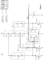
Figure 1 illustrates a schematic diagram of a switched-capacitor converter (SCC) having a compensation inductor the couples a first half-bridge to a second half-bridge of a rectifier. -
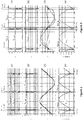
Figure 2 illustrates voltage and current waveforms within an SCC that uses zero-current switching (ZCS) but does not have a compensation inductor. -
Figure 3 illustrates voltage and current waveforms within an SCC that has a compensation inductor, such as the SCC ofFigure 1 . -
Figure 4 illustrates waveforms corresponding to switch voltages in the SCC ofFigure 1 and shows the zero-voltage switching (ZVS) achieved therein. -
Figures 5A, 5B ,5C, and 5D illustrate four power loops within the SCC ofFigure 1 . -
Figure 6 illustrates an alternative SCC which is similar to the SCC ofFigure 1 , but wherein compensation inductors are coupled between the first half-bridge rectifier and ground, and between the second half-bridge rectifier and ground. -
Figure 7 illustrates an alternative SCC which is similar to the SCC ofFigure 6 , but wherein a third half-bridge rectifier branch is included and another compensation inductor couples this third half-bridge rectifier branch to ground. -
Figure 8 illustrates a method for providing an SCC that includes a compensation inductor configured to couple a first half-bridge rectifier branch to a second half-bridge rectifier branch or a ground. -
Figure 9 illustrates a schematic diagram of a switched-capacitor converter (SCC) similar to that ofFigure 1 , but including additional switch stages. - The embodiments described herein provide circuits and methods that enable efficient operation of a switched-capacitor converter (SCC) while not requiring high-precision inductors and capacitors. This is achieved by introducing a compensation inductor that is not part of a resonant tank within the SCC, but which serves to transfer charge to or from switch capacitances when the switches are off, i.e., during dead-time intervals that occur between intervals when adjacent switches are conducting. By transferring charge (energy) to or from the compensation inductor when the switches are off, the voltage across a switch may be reduced to zero just before the switch is enabled, thereby providing zero-voltage soft switching (ZVS) and the efficiencies associated with such ZVS.
- In preferred embodiments, no inductor components are required in the resonant tanks of the SCC. Instead, the parasitic inductance of the traces and components (e.g., switches, capacitors) within a given power loop is used as a resonant inductance. Once the resonant inductance for a given power loop is characterized, a resonant capacitance may be determined to provide resonance at a given switching frequency. This, in turn, should provide nearly zero current switching (ZCS). Inaccuracy in the characterized resonant inductance or the resonant capacitance, as caused by component variation or temperature drift, may lead to a mismatch between the switching frequency and the resonant frequency for a given resonant leg of the SCC. Such a frequency mismatch causes loss of ZCS. While ideal ZCS and its associated efficiency may not be achieved due to such mismatch, the efficiency associated with the ZVS allows the SCC to still have good efficiency. Stated alternately, the soft-switching enabled by the compensation inductor makes efficient operation of SCC more tolerant to variation in the resonant inductance and capacitance, and the resonant frequency determined from these reactances.
- Note that resonant inductor components may be used within an SCC that also makes use of the compensation inductor, and such an SCC will achieve near ideal ZCS and ZVS. However, use of the compensation inductor and its associated ZVS provides the advantage that resonant inductor components may be eliminated, thereby reducing required space on a printed circuit board, reducing cost, and reducing inductor core loss. (Some of these advantages are partially offset by the need for larger resonant capacitors, but there is a net benefit in eliminating the resonant inductor components.) The use of a compensation inductor and no resonant inductor components also allows an SCC to use a higher switching frequency than SCCs that use resonant inductor components, which provides advantages including lower voltage ripple at the output of the SCC.
- The inventions are described below by way of particular examples. This description begins with an embodiment of an SCC that reduces an input voltage by a factor of four, i.e., a 4:1 SCC, and that includes a compensation inductor that provides ZVS (soft-switching). The compensation inductor is placed across two half-bridge branches of a rectifier. While the illustrated examples focus on a 4:1 SCC, it should be understood that the described techniques may be readily extrapolated to other SCC circuits including those that reduce an input voltage by 2:1, 6:1, 8:1, etc. The 4:1 SCC embodiment begins with a description of the circuitry used for implementing such a converter. This is followed by a description of waveforms for currents and voltages found within such an SCC. Circuit topologies in which compensation inductors are placed elsewhere are then described. Finally, a method for designing an SCC that makes use of a compensation inductor is described.
- It should be understood that the examples described below are not meant to be limiting. Circuits and techniques that are well-known in the art are not described in detail, so as to avoid obscuring the unique aspects of the invention. Features and aspects from the example embodiments may be combined or re-arranged, except where the context does not allow this.
-
Figure 1 illustrates an embodiment of a switched-capacitor converter (SCC) 100 that reduces the voltage provided at an input power supply VIN_DC by a factor of four. The reduced voltage is provided at an output VOUT_DC. The reduced voltage VOUT provided at the output VOUT_DC is typically an intermediate voltage, within a system, that must be stepped down further before being supplied to a load such as, e.g., a memory, a central processing unit (CPU). While not shown for ease of illustration, a switching DC/DC converter or a linear regulator coupled to the output VOUT_DC may provide this further step-down in voltage, and also provide regulation that is not provided by theSCC 100. In other applications, the reduced voltage VOUT provided by theSCC 100 may be used directly by a load. - The illustrated
SCC 100 includes afirst switch stage 110 which includes first and second switches Q1, Q2, and asecond switch stage 112 which includes third and fourth switches Q3, Q4. A rectifier is interposed between thesecond switch stage 112 and ground, and provides a rectified voltage VOUT to the output VOUT_DC and a filter capacitor COUT. The illustrated rectifier includes switches Q7 and Q8, which form a first half-bridge rectifier branch 140, and switches Q9 and Q10, which form a second half-bridge rectifier branch 146. The switches Q7, Q8 of the first half-bridge rectifier branch 140 are connected at a half-bridge switching node V4, whereas the switches Q9 and Q10 of the second half-bridge rectifier branch 146 are connected at another half-bridge switching node V5. - A compensation inductor, denoted LZVS, couples the first half-
bridge rectifier branch 140 to the second half-bridge rectifier branch 146 at their respective switching nodes V4, V5. As will be explained in detail further below, the compensation inductor LZVS provides a conduction path that serves to transfer charge to or from the capacitances Coss of the switches within the switch stages 110, 112 such that the voltage across these switches, e.g., the drain-to-source voltage Vds for a field effect transistor (FET), is reduced to zero before a given switch is turned on. In this way, the compensation inductor Lzvs enables zero voltage switching (ZVS) for each of the switches, regardless of whether resonant tanks of the circuit branches are matched to a switching frequency of theSCC 100. - The
SCC 100 further includes a firstresonant leg 120 that couples thefirst switch stage 110 to the rectifier, and a secondresonant leg 122 that couples thesecond switch stage 112 to the rectifier. The firstresonant leg 120 includes a first resonant capacitor CR1 and is characterized as having a first resonant inductance LR1. A resonant current IR1 flows through the firstresonant leg 120. The secondresonant leg 122 is similarly configured to include a second resonant capacitor CR2 and is characterized as having a second resonant inductance LR2. A resonant current IR2 flows through the secondresonant leg 122. As detailed below, the resonant inductances LR1, LR2 for the preferred embodiment merely represent the parasitic inductances within power loops of theSCC 100. - The first
resonant leg 120 couples a switching node V1 connecting the first and second switches Q1, Q2 of thefirst switch stage 110 to the switching node V4 connecting the switches Q7, Q8 of the first half-bridge rectifier branch 140. The secondresonant leg 122 similarly couples a switching node V3 connecting the third and fourth switches Q3, Q4 of thesecond switch stage 112 to the same switching node V4 connecting the switches Q7, Q8 of the first half-bridge rectifier branch 140. A first flyingleg 130 couples an inter-stage connection node V2 to the second half-bridge rectifier branch 146 at the connection node V5 between its switches Q9, Q10. The firstflying leg 130 includes a first flying capacitor CFLY1 and is characterized as having a first flying inductance LFLY1, which typically is not an inductor component. - The switches Q1,...Q4, Q7,...Q10 illustrated in the
SCC 100 ofFigure 1 are power metal-oxide semiconductor field-effect transistors (MOSFETs), but other switch types may be used. For example, junction field-effect transistors (JFETs), bipolar junction transistors (BJTs), insulated gate bipolar transistors (IGBTs), high electron mobility transistors (HEMTs), or other types of power transistors may be preferred in some applications. The switches Q1,...Q4, Q7,...Q10 may be integrated on the same semiconductor die, may each be provided on separate dies, or may otherwise be spread across a plurality of semiconductor dies. Each of the switches Q1,...Q4, Q7,...Q10 within theSCC 100 has drain and source terminals, as well as a gate terminal (not shown for ease of illustration) that controls conduction between the drain and source. A control signal is provided to each of the gate terminals via a driver, which is also not shown for ease of illustration. - The
SCC 100 further includes acontroller 150 which generates control signals for the switches Q1,...Q4, Q7,...Q10 of theSCC 100. Thecontroller 150 alternates between setting the first switch Q1 to conduct, while the second switch Q2 is off, and setting the second switch Q2 to conduct, while the first switch Q1 is off. Switching of the switches Q3, Q4 within thesecond switch stage 112 is similarly alternated, as is the switching of the switches Q7, Q8, Q10, Q9 within the first and second half-bridge rectifier branches controller 150 generates a pulse-width-modulated (PWM) control signal VPWM_QA that controls the switches Q1, Q3, Q7, Q10 within group A, and a PWM control signal VPWM_QB that controls the switches Q2, Q4, Q8, Q9 within group B. The switch control signals VPWM_QA, VPWM_QB are typically input to driver circuits for each of the switches. For theSCC 100 ofFigure 1 , the control signal VPWM_QA may be provided to 4 separate drivers which output control signals VPWM_Q1, VPWM_Q3, VPWM_Q7, VPWM_Q10 for the group A switches Q1, Q3, Q7, Q10. The control signal VPWM_QB may be provided to 4 separate drivers which output control signals VPWM_Q2, VPWM_Q4, VPWM_Q8, VPWM_Q9 for the group B switches. The control signals output from the drivers are then provided to control terminals (e.g., gates) of the switches. For ease of illustration, the drivers are not shown. In alternative implementations, thecontroller 150 may generate separate control signals for each of the switches, rather than providing common control signals VPWM_QA, VPWM_QB for the two switch groups. - Waveforms for the alternating control signals VPWM_QA, VPWM_QB are symmetric, i.e., have the same positive pulse intervals, such that each control signal has a duty cycle of approximately 50%. There is a dead time between pulses of the control signals VPWM_QA, VPWM_QB, i.e., for each switch cycle of the
SCC 100 there will be brief intervals during which none of the switches are conducting. Thecontroller 150 generates the control signals VPWM_QA, VPWM_QB at a switching frequency Fsw. For optimal efficiency, the resonant frequencies corresponding to theresonant legs SCC 100 should match the switching frequency Fsw, with a small adjustment to account for the dead time intervals. - The
controller 150 and its constituent parts may be implemented using a combination of analog hardware components (such as transistors, amplifiers, diodes, and resistors), and processor circuitry that includes primarily digital components. The processor circuitry may include one or more of a digital signal processor (DSP), a general-purpose processor, and an application-specific integrated circuit (ASIC). Thecontroller 150 may also include memory, e.g., non-volatile memory such as flash, that includes instructions or data for use by the processor circuitry, and one or more timers, e.g., for providing the switch intervals according to the switching frequency and dead time intervals. -
Figures 2-4 illustrate voltage and current waveforms within SCCs that implement soft switching of the switches within switch stages and rectifiers, such as within theSCC 100 ofFigure 1 . - The voltage and current waveforms of
Figure 2 correspond to an SCC that uses zero-current switching (ZCS), but that does not include a compensation inductor, such as LZVS withinFigure 1 , providing zero-voltage switching (ZVS). For ease of illustration, such a ZCS SCC is not shown but would resemble theSCC 100 ofFigure 1 , with the noteworthy exception that the compensation inductor LZVS is deleted. Additionally, the resonant inductances LR1, LR2 within a ZCS SCC are typically inductor components, rather than the preferred parasitic inductances described previously for theSCC 100. - The ZCS SCC corresponding to
Figure 2 has a switching frequency of 335 kHz. (The corresponding switching half-period is 1490 ns, which is reduced by a dead time of 80 ns yielding an active/conducting half-period of 1410 ns. When the switching frequency is thus derated by the dead time, the effective active switching frequency is 353 kHz.) The ZCS SCC has first and second resonant legs, which include resonant inductors LR1, LR2 with inductances of 70 nH and resonant capacitors inductors CR1, CR2 with capacitances of 2.82 µF. The resonant inductances will be further increased by the parasitic inductances of power loops that include the first and second resonant legs. For example, a first power loop that includes, in part, the first resonant leg may have a parasitic inductance LPARA1 = 7 nH. The inductor LR1, parasitic inductance LPARA1, and capacitor CR1 form a resonant tank having a resonant frequency given by:
- The resultant resonant frequency f_res = 342 kHz is very close to the desired frequency of 353 kHz. The currents IR1, IR2 within the first and second resonant legs take on sinusoidal shapes, as shown in the
current waveforms 230. Because the resonant frequency (e.g., approximately 342 kHz) of each resonant tank is well-matched to the effective active switching frequency (353 kHz), the switches are turned off when nearly zero current is flowing through them, as shown at times tOFF_QB, tOFF_QA withinFigure 2 . -
Figure 2 further illustratesvoltage waveforms 240 corresponding to control signals VPWM_QA, VPWM_QB for the switches of the ZCS SCC, and an output voltage VOUT of the ZCS SCC.Waveforms 220 corresponding to the drain-to-source voltages Vds_Q8, Vds_Q10 across the rectifier switches are shown, as arewaveforms 210 corresponding to the drain-to-source voltages Vds_Q1,... Vds_Q4 across switches within the switch stages. Note that the drain-to-source voltages Vds_Q1,... Vds_Q4 across switches within the switch stages do not drop to zero before these switches are turned on, e.g., at times tON_QA, tON_QB. While the SCC corresponding to the waveforms ofFigure 2 achieves ZCS, it does not achieve ZVS. - In order to achieve ZCS, or near ZCS, the resonant frequencies f_res corresponding to power loops (conduction paths) that include each of the resonant legs must be closely matched to each other and to the desired switching frequency. This, in turn, means that the inductance-capacitance product, as provided in equation (1), must be fairly precise. To achieve this, high-precision inductors and capacitors are typically required. In addition to having low tolerances, e.g., ± 5%, the resonant inductors and capacitors must be stable over temperature, and the capacitors must not have a high dependency on any DC bias voltage across them. Such high-precision, temperature-stable, bias-independent components are more expensive and larger than standard components. Hence, a ZCS SCC corresponding to the waveforms of
Figure 2 is relatively expensive, physically large, and does not achieve the switching efficiencies provided by ZVS. -
Figure 3 illustrates voltage and current waveforms similar to those ofFigure 2 , but corresponding to theZVS SCC 100 ofFigure 1 . The illustratedwaveforms 340 for the signals VPWM_QA, VPWM_QB that control the switches, and the output voltage VOUT of theSCC 100 are similar to thewaveforms 240 ofFigure 2 except, notably, that the switching frequency of theSCC 100 is 600 kHz rather than 335 kHz. However, theFigure 3 waveforms 330 corresponding to the resonant currents IR1, IR2, and theFigure 3 waveforms 310 corresponding to drain-to-source voltages for the switches Q1, Q2, Q3, Q4 differ substantially from those ofFigure 2 . -
Figure 4 illustrateswaveforms 410 corresponding to drain-to-source voltages Vds_Q1, Vds_Q2, Vds_Q3, Vds_Q4 across the switches Q1, Q2, Q3, Q4 of the switch stages 110, 112. Thesewaveforms 410 represent an expanded view ofsimilar waveforms 310 withinFigure 3 in the vicinity when thecontroller 150 turns off the switches within group A and turns on the switches within group B. So as to provide timing context for the drain-to-source voltages, waveforms for the switch control signals VPWM_QA, VPWM_QB are also shown. For the illustrated time interval prior to time tOFF_QA, the switches Q1, Q3 of group A are turned on, as indicated by the active high pulse on the group A control signal VPWM_QA, whereas the switches Q2, Q4 of group B are turned off. Because the group A switches Q1, Q3 are conducting (closed), the drain-to-source voltages Vds_Q1, Vds_Q3 across them is zero during this time interval. The drain-to-source voltages Vds_Q2, Vds_Q4 for the group B switches Q2, Q4, which are not conducting (i.e., open), will float, respectively, to twice the output voltage VOUT and to the output voltage VOUT during this time interval. For a voltage of 54V provided by the input power supply VIN_DC, the resultant voltage Vds_Q2 across the second switch Q2 is 27V, whereas the resultant voltage Vds_Q4 across the fourth switch Q4 is 13.5V. - At time TOFF_QA, the control signal VPWM_QA for group A transitions to a low value so as to turn off the group A switches Q1, Q3. This means that none of the switches are conducting, i.e., they are all open until time tON_QB. This interval when no switches are conducting is often termed dead time. Referring to the second switch Q2 of the
SCC 100, the compensation inductor LZVS provides a conduction path from the drain of this switch, i.e., from the first switching node V1 within theSCC 100 ofFigure 1 . During the dead-time, charge stored on the capacitance COSS of the second switch Q2 will be discharged by current IZVS conducted through the compensation inductor LZVS. Provided adequate current flow IR1 (charge transfer) from the drain of the second switch Q2 during the dead time, the voltage at this drain (i.e., node V1) will be reduced from 3*VOUT to 1*VOUT, which matches the voltage at the source (i.e., node V2) of the second switch Q2 at the end of the dead time. Hence, the drain-to-source voltage Vds_Q2 across the second switch Q2 is reduced to zero before time tON_QB. With zero voltage across the second switch Q2 when it is turned on at time TON_QB, ZVS (soft switching) is achieved. - The drain of the fourth switch Q4 is similarly discharged during the dead time. More particularly, the compensation inductor LZVS enables current IR2 to flow through the second
resonant leg 122, thereby discharging stored charge on the capacitance COSS of the fourth switch Q4. Provided adequate current flow IR2 (charge transfer) from the drain of the fourth switch Q4 during the dead time, the voltage at this drain (i.e., at node V3) will be reduced from 2*VOUT to 1*VOUT, which matches the voltage at the source of the fourth switch Q4 (i.e., at node VOUT_DC) at the end of the dead time. Hence, the drain-to-source voltage Vds_Q4 across the fourth switch Q4 is reduced to zero before time tON_QB, thereby achieving zero-voltage soft switching (ZVS) for the turn on of the fourth switch Q4 at time tON_QB. - During the described dead time, the currents IR1, IR2 flowing through the
resonant legs bridge rectifier branch 140, as its switches Q7, Q8 are turned off.) During this dead time, energy is transferred out of the capacitances COSS of the second and fourth switches Q2, Q4 and stored in the compensation inductor LZVS. The inductor current IZVS is illustrated in thewaveforms 330 ofFigure 3 , where a peak current magnitude of 10A flows during each of the illustrated dead times. - A second dead time occurs between the point in time when the switches within group B are turned off and the point in time when the switches of group A are turned on, i.e., between the time tOFF_QB and the time TON_QA in
Figure 3 . This second dead time interval is not illustrated in an expanded view. The circuit operation during this second dead time complements the operation described above. During the second dead time, currents IR1, IR2 through the resonant legs flow in the opposite direction to that described previously, and serve to charge the source of the first and third switches Q1, Q3. Energy is transferred from the compensation inductor LZVS to the capacitances COSS of these switches Q1, Q3. The source voltages, as provided at the nodes V1, V3, is increased during the second dead time until these voltages match, respectively, the drain voltages for these switches Q1, Q3. In other words, the drain-to-source voltages Vds_Q1, Vds_Q3 are reduced to zero during the second dead time, thereby achieving zero-voltage soft switching (ZVS) when the group A switches Q1, Q3 are turned on. - The compensation inductor LZVS within the
SCC 100 must be capable of handling the peak current required to achieve the above-described ZVS, i.e., such that adequate charge can be transferred during the dead times. This peak current is determined by the sum of all charges QOSS that must be drained from (or provided to) the switch capacitances COSS for each switch group. The charge accumulation on a given switch capacitor COSS depends upon its capacitance and upon the resonant frequency mismatch within theSCC 100. A mismatched resonant frequency leads to current flow through a switch when that switch is turned off, i.e., ZCS is not achieved. At the instant when the switch is disabled, the residual current flow causes charge accumulation on the switch capacitance COSS. - The current flowing through each of the resonant legs must be capable of discharging (charging) the charge QOSS of its associated switch within the prescribed dead time tDT. The compensation inductor LZVS must support the current flows through all of the resonant legs. In the specific example based upon the
SCC 100, the COSS of the MOSFET switches, the resonant frequency mismatch leading to the non-zero resonant currents IR1, IR2 when they are turned off, and the dead time tDT of 60 ns lead to the peak current magnitude of 10A which is illustrated in thecurrent waveforms 330 ofFigure 3 . An SCC having better resonant frequency matching will require lower peak current magnitudes, as will SCCs that use longer dead times. The switch capacitance Coss or similar also has a significant effect on charge accumulation and the associated peak current requirement. The switch capacitance is largely a function of the type of switch, and may be significantly different for switches other than the MOSFETs described for theSCC 100 ofFigure 1 . -
Figure 3 further illustrateswaveforms 330 corresponding to resonant currents IR1, IR2 flowing in the first and secondresonant legs SCC 100. A similar mismatch occurs for the secondresonant leg 112, leading to nonzero current IR2 at time tOFF_QA when the third switch Q3 is turned off. - The mismatches in the resonant frequencies for the positive vs. negative half-cycles are not a significant problem in the
current waveforms 230 illustrated inFigure 2 . As previously described, the ZCS SCC includes actual inductor components LR1, LR2 within theresonant legs - The situation is quite different for the
SCC 100 ofFigure 1 if there are no inductor components and the resonant inductances LR1, LR2 are provided solely by parasitic inductances. Variation in the length of traces and/or number of elements within the power loops (conduction paths) may yield significantly different parasitic inductances, resulting in the resonant frequency mismatches evident in thecurrent waveforms 330 ofFigure 3 . This will be further explained using the power loops (conduction paths) illustrated inFigures 5A-5D . For ease of illustration, some of the demarcations shown in theSCC 100 ofFigure 1 have been deleted inFigures 5A-5D , but the underlying circuit connections are the same as inFigure 1 . Also for ease of illustration, thecontroller 150 is not shown inFigures 5A-5D . -
Figures 5A and 5B illustratepower loops Figures 5C and 5D illustratepower loops Figures 5A and5C . - A reactance of the illustrated
conduction path 510 from node 1 (VIN_DC) to node 2 (VOUT_DC) determines a resonant frequency for the first resonant current IR1 when this current is in a positive half cycle. In designing theSCC 100, a parasitic inductance of this path may be characterized via circuit simulation or measurement. If theSCC 100 is implemented on a printed circuit board (PCB), then this inductance includes the parasitic inductances of the first switch Q1, the first resonant capacitor CR1, a half-bridge switch Q7, and the PCB traces that connect these elements. (An integrated circuit implementation may instead characterize the parasitic inductance of traces on a die.) Once this inductance is characterized, a capacitance for the first resonant capacitor may be chosen based upon a given switching frequency and dead time. For example, if the parasitic inductance of thispath 510 is 1 nH and the controller uses a switching frequency of 600 kHz (switching half-period of 833 ns) with a dead time of 60 ns (active switching half period of 773 ns), then the first resonant capacitor CR1 would be designed with a capacitance of 60 µF. With such a configuration, the first resonant current IR1 would take on a half-sinusoidal shape that would fall to zero 770 ns after its initial rise. (Seeequation 1.) This is shown in thewaveform 330 for the first resonant current IR1 withinFigure 3 , which begins rising at time tON_QA_0, when the first switch Q1 is turned on, and falls to zero approximately 770 nsec later at time tOFF_QA, when this switch Q1 is turned off. - After a dead time tDT, the switches within group B are turned on at time tON_QB. This results in current conduction through the
power loop 530 illustrated inFigure 5C . A reactance of the illustratedconduction path 530 from node 1 (VOUT-DC) to node 2 (ground) determines a resonant frequency for the first resonant current IR1 when this current is in a negative half cycle. If theSCC 100 is implemented on a printed circuit board (PCB), then this inductance includes the parasitic inductances of the second switch Q2, the first resonant capacitor CR1, half-bridge switches Q8 and Q9, the first flying capacitor CFLY1, and the PCB traces that connect these elements. This inductance will be larger than the 1 nH inductance of thepower loop 510, due to the additional switch, additional capacitor, and the additional traces. The first flying capacitor CFLY1 also affects the resonant capacitance for thepower loop 530. For CFLY1 = 40 µF and CR1 = 60 µF, the overall resonant capacitance of thepower loop 530 is 24 µF, which is considerably smaller than the resonant capacitance of thepower loop 510. The different reactance of thepower loop 530 leads to a different resonant frequency for the negative half-cycle of the first resonant current IR1. This is shown in thecurrent waveforms 330 ofFigure 3 , wherein the second switch Q2 is turned off while current is still flowing through it at time tOFF_QB, i.e., zero current switching (ZCS) is not achieved for the negative half-cycle of the first resonant current IR1 that flows through the second switch Q2 and the switches Q8, Q9 of the rectifier. - Conduction paths for the second resonant current IR2 are shown in the
power loop 520 ofFigure 5B and thepower loop 540 ofFigure 5D . The relationship between the reactances of thepower loops waveforms 330 ofFigure 3 , the positive half-cycle for the second resonant current IR2 does not achieve ZCS due to a mismatch in the resonant frequency of thepower loop 520 and the switching frequency. However, the negative half-cycle for the second resonant current IR2 does achieve ZCS as the resonant frequency of thepower loop 540 closely matches the switching frequency. - The
SCC 100 ofFigure 1 shows a compensation inductor Lzvs coupling two half-bridge rectifier branches within a 4:1 SCC. However, other circuit topologies may connect compensation inductors in other ways, and still other circuits may provide other conversion ratios. - The
controller 150 withinFigure 1 is presumed to generate symmetric control signals VPWM_QA, VPWM_QB, i.e., PWM waveforms that have 50% duty cycle except for the dead time. If non-symmetric PWM signals are generated, e.g., having a duty cycle other than 50%, then the energy stored and released from the compensation inductor LZVS may not be perfectly balanced and the compensation inductor Lzvs may saturate. This issue may be addressed by placing a DC blocking capacitor in series with the compensation inductor LZVS. (For ease of illustration, such a circuit is not shown.) - The
SCC 100 ofFigure 1 uses twoswitch stages SCC 100 may be readily extrapolated to provide other conversion ratios. For example, thesecond conversion stage 112, the secondresonant leg 122, and the first flyingleg 130 may be deleted to yield an SCC having a 2:1 conversion ratio. Conversely and as shown in theSCC 900 illustrated inFigure 9 , athird switch stage 114 may be interposed between thesecond switch stage 112 and the rectifier, and have an associated thirdresonant leg 124 and an associated second flyingleg 132. These components would be connected in a manner similar to thesecond switch stage 112, the secondresonant leg 122, and the first flyingleg 130 of theSCC 100. The resultant SCC would have a down-conversion of 6:1. This technique could be repeated to achieve down-conversions of 8:1 and beyond. For ease of illustration, circuits having these alternative down-conversion ratios are not explicitly illustrated. -
Figure 6 illustrates analternative SCC circuit 600 in which a first compensation inductor LZVS1 is connected between the first half-bridge rectifier branch 140, at a half-bridge switch node V4, and ground. A first DC blocking capacitor CDC_BLK1 is placed in series with the first compensation inductor LZVS1 so that the DC voltage at the half-bridge switch node V4 is not undesirably impacted by the first compensation inductor LZVS1. A flying compensation inductor LZVS_F1 and a flying DC blocking capacitor CDC_BLK_F1 connect the first flyingleg 130 to ground and enable charging/discharging of capacitances for the second and third switches Q2, Q3. -
Figure 7 illustrates anotheralternative SCC circuit 700 in which a third half-bridge rectifier branch 142 is provided to support the secondresonant leg 122 and its associated second resonant current IR2. By splitting the resonant currents IR1, IR2 between two half-bridge rectifier branches bridge rectifier branch 140 is used to support bothresonant legs SCC 100 ofFigure 1 and theSCC 600 ofFigure 6 . Thealternative SCC 700 also includes a second compensation inductor LZVS2 and a second DC blocking capacitor CDC_BLCK2, which are coupled to the secondresonant leg 122 and serve to discharge and charge, respectively, capacitances of the third and fourth switches Q3, Q4 - The
SCC 600 ofFigure 6 includes two half-bridge rectifier branches bridge rectifier branch 146 may be deleted, leading to half-wave rectification for the voltage VOUT provided at the output VOUT_DC. -
Figure 8 illustrates amethod 800 for providing a switched-capacitor converter (SCC) that converts power from a power supply at an input into power at an output. Thismethod 800 may be used to design an SCC such as theSCC 100 ofFigure 1 . The method provides 810 a rectifier at the output of the SCC, provides 820 a first switch stage, and provides 830 a first resonant leg. The first switch stage includes first and second switches connected in series at a first connection node, wherein the first switch stage is interposed between the input and the rectifier. The first resonant leg comprises a first resonant capacitor coupled between the first connection node and a first rectifier branch of the rectifier. - A first power loop of the SCC connects the input to the output and includes the first switch, the first resonant leg, a rectifier switch within the first rectifier branch and traces connecting these elements. The method proceeds by characterizing 840 a first resonant inductance of this first power loop. A switching frequency is determined 850 for the SCC. A first capacitance for the first resonant capacitor is then determined 860 based upon the first resonant inductance and the switching frequency, e.g., using equation (1). Finally, a compensation inductor is provided 870 and couples the first rectifier branch to either a second branch of the rectifier, or a ground.
- The characterization of the first resonant inductance is typically performed by simulating the inductances of elements and traces on an SCC that is being designed, but may also be accomplished by measuring inductances on an SCC circuit.
- The capacitance of a capacitor component typically varies according to the DC voltage applied across the capacitor. For example, a standard capacitor with a rated value of 10 µF for no DC bias may have a nominal capacitance of 8.9 µF when a 13.5 V DC bias is applied across it, a capacitance of 5.5 µF when a 27 V DC bias is applied across it, and a capacitance of 3.5 µF when a 40.5 V DC bias is applied across it. Within an SCC such as the
SCC 100 ofFigure 1 , the first resonant capacitor CR1 will typically have a fairly significant bias voltage of 40.5 V (3*VOUT) across it. Such a bias voltage should be taken into account when choosing resonant capacitors for an SCC. - Presume that a first capacitance of 20 µF is determined for the first resonant capacitor, and that a DC bias of 40.5 V is expected across this capacitor. According to the above-described dependence of capacitance on DC bias, a 10 µF would only yield 3.5 µF at a 40.5 V DC bias. To achieve the desired capacitance of 20 µF, 6 of the capacitors rated at 10 µF would be placed in parallel to form the desired first resonant capacitor, thereby resulting in a capacitance of 21 µF at a DC bias of 40.5 V.
- The
method 800 may be extended to characterize a second resonant inductance within a second power loop, or further resonant inductances corresponding to further power loops. Such characterizations may use techniques similar to those described in relation toFigures 5B-5D . Second and further capacitances may then be determined based upon the second and further resonant inductances. - The resonant frequencies of power loops (conduction paths) within an SCC may not be perfectly matched. The method may further be extended to characterize mismatches in such resonant frequencies, and to determine an inductance and power rating for the compensation inductor based on these mismatches.
- The
method 800 may also be extended to provide additional switch stages, resonant legs, and flying legs, as shown in theSCC 100 ofFigure 1 . - It is to be understood that the features of the various embodiments described herein may be combined with each other, unless specifically noted otherwise.
Claims (20)
- A switched-capacitor converter comprising:an input for coupling to an input power supply;an output for providing power to a load;a rectifier (140, 146) at the output;a first switch stage (110) comprising a first switch (Q1) and a second switch (Q2) connected in series at a first connection node (V1) and interposed between the input and the rectifier (140, 146);a first resonant leg (120) comprising a first resonant capacitor (CR1) that couples the first connection (V1) node to a first rectifier branch (140) of the rectifier (140, 146);a controller (150) operable to alternate switching of the first switch (Q1) and second switch (Q2), so as to transfer energy from the input to the output, and wherein the switching is performed at a switch frequency chosen to approximate zero current switching conditions for each of the switches (Q1, Q2); anda first compensation inductor (LZVS; LZVS1) that couples the first rectifier branch (140) to a second rectifier branch (146) of the rectifier (140, 146) or to a ground.
- The switched-capacitor converter of claim 1, wherein the first resonant leg (120) has an associated first resonant inductance (LR1), and wherein a capacitance of the first resonant capacitor (CR1) is determined such that the switch frequency is a resonant frequency of the first resonant capacitor (CR1) and the first resonant inductance (LR1).
- The switched-capacitor converter of claim 2, wherein the first resonant inductance (LR1) is provided by parasitic inductances within a first power loop connecting the input to the output, the first power loop comprising the first switch (Q1), the first resonant leg (120), a rectifier switch within the first rectifier branch (140) and traces connecting these elements.
- The switched-capacitor converter of claim 3, wherein the first resonant inductance (LR1) does not include an inductor component.
- The switched-capacitor converter of any one of the preceding claims, further comprising a direct-current (DC) blocking capacitor (CDC_BLK1) connected in series with the first compensation inductor (LZVS1).
- The switched-capacitor converter of any one of claims 1 to 5, wherein the first switch stage (110) is directly coupled to the first rectifier branch (140).
- The switched-capacitor converter of any one of claims 1 to 5, further comprising:a second switch stage (112) comprising a third switch (Q3) and a fourth switch (Q4) connected in series at a second connection node (V2) and interposed between the first switch stage (110) and the rectifier (140, 146);a second resonant leg (122) comprising a second resonant capacitor (CR2) that couples the second connection node (V3) to the rectifier; anda first flying leg (130) comprising a first flying capacitor (CFLY1) that couples a first inter-stage node (V2) connecting the first and second switch stages (110, 112) to the second rectifier branch (146) or to the ground,wherein the controller (150) is further operable to switch the third switch (Q3) in the same manner as the first switch (Q1), and to switch the fourth switch (Q4) in the same manner as the second switch (Q2).
- The switched-capacitor converter of claim 7, wherein the first flying leg (130) further comprises a first flying inductance (LFLY1) in series with the first flying capacitor (CFLY1).
- The switched-capacitor converter of claim 7 or 8, wherein the first flying inductance (LFLY1) is provided by parasitic inductances of traces connecting the first flying capacitor (CFLY1) to the first inter-stage node (V2) and to the second rectifier branch (146) or to the ground.
- The switched-capacitor converter of any one of claims 7 to 9, wherein the second resonant leg (122) and the first resonant leg (120) are coupled together at the first rectifier branch (140).
- The switched-capacitor converter of claim 10, further comprising:a direct-current (DC) blocking capacitor (CDC-BLK1) connected in series with the first compensation inductor (LZVS1),wherein the serially-connected first compensation inductor (LZVS1) and DC blocking capacitor (CDC_BLK1) couple the first and second resonant legs (120, 122) to the ground.
- The switched-capacitor converter of any one of claims 7 to 10, further comprising:a first direct-current (DC) blocking capacitor (CDC_BLK1) connected in series with the first compensation inductor (LZVS1), wherein the serially-connected first compensation inductor (LZVS1) and first DC blocking capacitor (CDC_BLK1) are coupled between the first resonant leg (120) and the ground;a second compensation inductor (LZVS2) connected in series with a second DC blocking capacitor (CDC-BLK2), wherein the serially-connected second compensation inductor (LZVS2) and second DC blocking capacitor (CDC-BLK2) are coupled between the second resonant leg (122) and the ground, andwherein the rectifier comprises a third rectifier branch (142) and the second resonant leg (122) is coupled to the third rectifier branch (142).
- The switched-capacitor converter of any one of claims 7 to 12, further comprising one or more additional capacitor-switch stages, each of which includes:an additional switch stage (114) comprising an additional high-side switch and an additional low-side switch connected in series at an additional connection node and interposed between the second switch stage (112) and the rectifier (140, 146);an additional resonant leg (124) comprising an additional resonant capacitor that couples the additional connection node to the rectifier (140, 146); andan additional flying leg (132) comprising an additional flying capacitor that couples an inter-stage node to the second rectifier branch (146) or to the ground, the inter-stage node connecting the additional switch stage (114) to another switch stage,wherein the controller (150) is further operable to switch the additional high-side switch in the same manner as the first switch (Q1), and to switch the additional low-side switch in the same manner as the second switch (Q2).
- The switched-capacitor converter of any one of the preceding claims, wherein an inductance and a power rating of the first compensation inductor (LZVS, LZVS1) are based upon a peak current in the first compensation inductor (LZVS, LZVS1) and a dead-time interval during which no switches within the first switch stage (110) are conducting.
- The switched-capacitor converter of claim 14, wherein the peak current is based upon a mismatch in resonant frequencies for different power loops of the switched-capacitor converter.
- A method for providing a switched-capacitor converter that converts power from a power supply at an input into power at an output, the method comprising:providing a rectifier (140, 146) at the output;providing a first switch stage (110) having a first switch (Q1) and a second switch (Q2) connected in series at a first connection node (V1), wherein the first switch (Q1) stage is interposed between the input and the rectifier (140, 146);providing a first resonant leg (120) that comprises a first resonant capacitor (CR1) coupled between the first connection node (V1) and a first rectifier branch (140) of the rectifier (140, 146);characterizing a first resonant inductance (LR1) within a first power loop connecting the input to the output, the first power loop comprising the first switch (Q1), the first resonant leg (120), a rectifier switch within the first rectifier branch (140) and traces connecting these elements;determining a switching frequency for the switched-capacitor converter;determining a first capacitance for the first resonant capacitor (CR1) based upon the first resonant inductance (LR1) and the switching frequency; andproviding a compensation inductor (LZVS, LZVS1) that couples the first rectifier branch (140) to either a second branch (146) of the rectifier (140, 146), or a ground.
- The method of claim 16, wherein the traces connecting the elements of the first power loop comprise traces on a printed circuit board (PCB).
- The method of claim 16 or 17, wherein the first resonant inductance (LR1) is characterized by simulating inductances of the elements and traces of the first power loop.
- The method of claim 16 or 17, wherein the first resonant inductance (LR1) is characterized by measuring inductances of the elements and traces of the first power loop.
- The method of claim 16, wherein determining the first capacitance is further based upon a derating of the first capacitance based upon a direct current (DC) voltage expected across the first resonant capacitor (CR1).
Applications Claiming Priority (1)
| Application Number | Priority Date | Filing Date | Title |
|---|---|---|---|
| US15/848,782 US10224803B1 (en) | 2017-12-20 | 2017-12-20 | Switched capacitor converter with compensation inductor |
Publications (2)
| Publication Number | Publication Date |
|---|---|
| EP3503367A1 true EP3503367A1 (en) | 2019-06-26 |
| EP3503367B1 EP3503367B1 (en) | 2024-10-23 |
Family
ID=64746025
Family Applications (1)
| Application Number | Title | Priority Date | Filing Date |
|---|---|---|---|
| EP18213802.4A Active EP3503367B1 (en) | 2017-12-20 | 2018-12-19 | Switched capacitor converter with compensation inductor |
Country Status (4)
| Country | Link |
|---|---|
| US (3) | US10224803B1 (en) |
| EP (1) | EP3503367B1 (en) |
| KR (1) | KR102668373B1 (en) |
| CN (1) | CN109980932B (en) |
Cited By (3)
| Publication number | Priority date | Publication date | Assignee | Title |
|---|---|---|---|---|
| TWI742852B (en) * | 2020-05-07 | 2021-10-11 | 立錡科技股份有限公司 | Resonant switching power converter |
| TWI742851B (en) * | 2020-04-20 | 2021-10-11 | 立錡科技股份有限公司 | Power converter |
| TWI746163B (en) * | 2020-05-26 | 2021-11-11 | 立錡科技股份有限公司 | Resonant switching power converter |
Families Citing this family (51)
| Publication number | Priority date | Publication date | Assignee | Title |
|---|---|---|---|---|
| CN109792205B (en) * | 2016-10-06 | 2020-10-30 | 株式会社村田制作所 | DC-DC converter |
| EP3379678B1 (en) * | 2017-03-23 | 2022-11-02 | Solaredge Technologies Ltd. | Balancer circuit |
| US10784777B2 (en) * | 2017-12-28 | 2020-09-22 | Texas Instruments Incorporated | Output current boosting of capacitor-drop power supplies |
| US10873260B2 (en) * | 2018-03-12 | 2020-12-22 | Analog Devices International Unlimited Company | Zero-voltage switching hybrid switched-capacitor converter |
| US10439493B1 (en) * | 2018-05-01 | 2019-10-08 | Semiconductor Components Industries, Llc | Methods and systems of operating a resonant dickson converter |
| US10903738B2 (en) * | 2018-05-14 | 2021-01-26 | Analog Devices International Unlimited Company | High conversion-ratio hybrid switched power converter |
| CN108712073B (en) * | 2018-06-08 | 2020-01-03 | 南京矽力杰半导体技术有限公司 | Three-level DC-DC converter |
| CN108736709B (en) | 2018-06-14 | 2020-02-04 | 南京矽力杰半导体技术有限公司 | Power converter |
| US20190393782A1 (en) * | 2018-06-25 | 2019-12-26 | Mykhaylo Teplechuk | Combined inductive and switched capacitive power supply conversion |
| US11152854B2 (en) * | 2018-08-10 | 2021-10-19 | The Regents Of The University Of Colorado, A Body Corporate | Hybrid converter family and methods thereof |
| CN109617394B (en) * | 2018-12-05 | 2021-08-17 | 成都芯源系统有限公司 | Resonant switch capacitor converter and controller and control method thereof |
| TWI691156B (en) * | 2018-12-22 | 2020-04-11 | 緯穎科技服務股份有限公司 | Power supply system, switched-tank converter and power supply method thereof |
| US10651731B1 (en) * | 2019-01-31 | 2020-05-12 | Infineon Technologies Austria Ag | Zero voltage switching of interleaved switched-capacitor converters |
| US11290008B2 (en) * | 2019-03-29 | 2022-03-29 | Mediatek Singapore Pte. Ltd. | Resonant switched-capacitor converter |
| CN111953206B (en) * | 2019-05-14 | 2022-03-25 | 台达电子企业管理(上海)有限公司 | Control method of DC converter, DC converter and readable storage medium |
| US12051972B2 (en) * | 2019-05-23 | 2024-07-30 | Infineon Technologies Austria Ag | Hybrid resonant power supply |
| JP7354629B2 (en) * | 2019-07-11 | 2023-10-03 | 富士電機株式会社 | Flying capacitor circuits, circuit modules and power conversion equipment |
| CN110518807B (en) * | 2019-08-09 | 2020-11-03 | 深圳市海浦蒙特科技有限公司 | Method and system for adjusting resonant frequency of push-pull soft switching circuit |
| KR102355293B1 (en) * | 2019-09-27 | 2022-01-25 | 주식회사 실리콘마이터스 | Switched-capacitor converter |
| US12237764B2 (en) * | 2019-12-02 | 2025-02-25 | The Regents Of The University Of California | Switching methods for regulating resonant switched-capacitor converters |
| CN111628556B (en) * | 2020-03-14 | 2023-06-16 | 青岛鼎信通讯股份有限公司 | Control strategy for improving DCDC efficiency of charging station based on energy router |
| TWI767346B (en) * | 2020-05-20 | 2022-06-11 | 立錡科技股份有限公司 | Resonant switching power converter |
| TWI742914B (en) * | 2020-06-08 | 2021-10-11 | 立錡科技股份有限公司 | Two-stage power converter |
| TWI755143B (en) * | 2020-06-19 | 2022-02-11 | 立錡科技股份有限公司 | Resonant switching power converter |
| JP2023531558A (en) * | 2020-06-30 | 2023-07-24 | ファーウェイ デジタル パワー テクノロジーズ カンパニー リミテッド | Power supply system and ICT equipment |
| TWI755144B (en) * | 2020-07-24 | 2022-02-11 | 立錡科技股份有限公司 | Resonant switching power converter |
| CN114342236B (en) * | 2020-07-29 | 2024-07-05 | 华为数字能源技术有限公司 | Conversion circuits and related electronic equipment |
| CN114070041B (en) * | 2020-08-03 | 2023-07-28 | 上海南芯半导体科技股份有限公司 | Resonance charge pump with zero-voltage switch and control method thereof |
| TWI740619B (en) * | 2020-08-21 | 2021-09-21 | 國立臺灣科技大學 | Control circuit and control method for power converter |
| EP4243265A4 (en) * | 2020-11-27 | 2023-12-20 | Huawei Technologies Co., Ltd. | RESONANT SWITCHED CAPACITOR DC/DC CONVERTER AND POWER SUPPLY SYSTEM |
| CN114696602B (en) * | 2020-12-31 | 2025-06-06 | 台达电子工业股份有限公司 | Power conversion circuit |
| CN114865917B (en) * | 2021-02-04 | 2025-06-06 | 台达电子工业股份有限公司 | Power conversion circuit |
| CN114915174B (en) * | 2021-02-09 | 2025-07-29 | 台达电子企业管理(上海)有限公司 | Non-isolated hybrid resonant circuit |
| CN113346738B (en) * | 2021-05-19 | 2025-01-07 | 南京矽力微电子技术有限公司 | A switched capacitor converter |
| CN113315372B (en) * | 2021-05-26 | 2023-02-10 | 南京矽力微电子技术有限公司 | Power converter |
| CN113644820B (en) * | 2021-08-24 | 2025-07-22 | 南京能利芯科技有限公司 | Power conversion topology of multi-phase switch capacitor resonant cavity conversion circuit with full-wave output rectification and power conversion structure based on power conversion topology |
| JP2023050261A (en) * | 2021-09-30 | 2023-04-11 | サンケン電気株式会社 | DC-DC converter |
| US12301108B2 (en) * | 2021-11-12 | 2025-05-13 | Southchip Semiconductor Technology (Shanghai) Co., Ltd. | Cascade switched capacitor converter to reduce switching loss |
| US20230155490A1 (en) * | 2021-11-12 | 2023-05-18 | Shanghai Nanxin Semiconductor Technology Co., Ltd. | Biphasic dickson switched capacitor converters with zero voltage switching |
| US12627225B2 (en) * | 2021-11-12 | 2026-05-12 | Southchip Semiconductor Technology (Shanghai) Co., Ltd. | Switched capacitor converter |
| KR102678371B1 (en) * | 2021-12-17 | 2024-06-26 | 주식회사 실리콘마이터스 | Switched-capacitor converter |
| CN116915050B (en) * | 2022-04-19 | 2026-06-02 | 立锜科技股份有限公司 | Power converter and its control method |
| CN117240096A (en) * | 2022-06-06 | 2023-12-15 | 华为技术有限公司 | Converters and electronic equipment |
| CN115276425B (en) * | 2022-08-05 | 2025-11-07 | 阳光电源股份有限公司 | Power converter and control method of neutral point potential fluctuation suppression circuit thereof |
| US12273046B2 (en) * | 2022-12-07 | 2025-04-08 | Dell Products L.P. | Hybrid voltage regulator architecture |
| US12614978B2 (en) | 2023-01-20 | 2026-04-28 | Infineon Technologies Austria Ag | Capacitor converter |
| CN118508737A (en) * | 2023-02-15 | 2024-08-16 | 台达电子工业股份有限公司 | Totem-pole power factor corrector with zero voltage switching |
| CN118337064B (en) * | 2024-04-17 | 2025-10-10 | 西安电子科技大学 | A resonant switched capacitor converter using PCB trace integrated inductor |
| CN118100890B (en) * | 2024-04-28 | 2024-06-28 | 成都市易冲半导体有限公司 | A power supply circuit and control method thereof and switched capacitor circuit |
| CN118842289B (en) * | 2024-06-28 | 2025-10-03 | 华中科技大学 | A two-stage voltage converter with self-balancing flying capacitor voltage |
| EP4760590A1 (en) * | 2024-12-11 | 2026-06-17 | EM Microelectronic-Marin SA | Low frequency differential resonant capacitor |
Family Cites Families (44)
| Publication number | Priority date | Publication date | Assignee | Title |
|---|---|---|---|---|
| US4178612A (en) | 1978-07-21 | 1979-12-11 | Texas Instruments Incorporated | Delta frame circuit |
| DE2851789C2 (en) | 1978-11-30 | 1981-10-01 | Licentia Patent-Verwaltungs-Gmbh, 6000 Frankfurt | Circuit for switching and transmitting alternating voltages |
| US4814962A (en) * | 1988-05-27 | 1989-03-21 | American Telephone And Telegraph Company, At&T Bell Laboratories | Zero voltage switching half bridge resonant converter |
| US5101334A (en) | 1989-02-14 | 1992-03-31 | U.S. Philips Corporation | High speed power supply circuit with circuit with positive feedback |
| US5581454A (en) * | 1994-11-22 | 1996-12-03 | Collins; Hansel | High power switched capacitor voltage conversion and regulation apparatus |
| US6429632B1 (en) * | 2000-02-11 | 2002-08-06 | Micron Technology, Inc. | Efficient CMOS DC-DC converters based on switched capacitor power supplies with inductive current limiters |
| US8008901B2 (en) | 2006-02-28 | 2011-08-30 | Infineon Technologies Austria Ag | Regulated power supply with multiple regulators sharing the total current supplied to a load |
| US6853569B2 (en) * | 2003-01-17 | 2005-02-08 | The Hong Kong Polytechnic University | DC to DC converter |
| JP5151266B2 (en) * | 2007-06-20 | 2013-02-27 | 株式会社リコー | Switching regulator and switching regulator operation control method |
| US7821305B1 (en) | 2008-04-03 | 2010-10-26 | Atheros Communications, Inc. | Dual voltage buffer with current reuse |
| US8674669B2 (en) * | 2008-10-16 | 2014-03-18 | Silergy Semiconductor Technology (Hangzhou) Ltd | Switching regulator with a single inductor in a multiple output power supply configuration |
| JP2010119226A (en) | 2008-11-13 | 2010-05-27 | Elpida Memory Inc | Charge pump circuit |
| US8423800B2 (en) * | 2009-12-22 | 2013-04-16 | Intel Corporation | Switched capacitor voltage regulator with high efficiency over a wide voltage range |
| US20110169474A1 (en) * | 2010-01-09 | 2011-07-14 | Cuks, Llc | Step-down switching PFC converter |
| CA3025336A1 (en) * | 2010-09-30 | 2012-03-30 | Philips Lighting Holding B.V. | Apparatus and methods for supplying power |
| US10389235B2 (en) * | 2011-05-05 | 2019-08-20 | Psemi Corporation | Power converter |
| US9024478B2 (en) | 2011-03-03 | 2015-05-05 | Massachusetts Institute Of Technology | Photovoltaic energy extraction with multilevel output DC-DC switched capacitor converters |
| WO2013086445A1 (en) * | 2011-12-09 | 2013-06-13 | The Regents Of The University Of California | Switched-capacitor isolated led driver |
| US8723491B2 (en) * | 2011-12-19 | 2014-05-13 | Arctic Sand Technologies, Inc. | Control of power converters with capacitive energy transfer |
| TWI482410B (en) | 2012-06-28 | 2015-04-21 | Niko Semiconductor Co Ltd | Multiphase dc-to-dc converter |
| WO2014024184A1 (en) * | 2012-08-05 | 2014-02-13 | Ben-Gurion University Of The Negev Research & Development Authority | A high efficiency resonant switched capacitor converter with continuous conversion ratio |
| KR101315143B1 (en) | 2012-08-22 | 2013-10-14 | 전북대학교산학협력단 | High efficiency dc/dc power converter with high conversion ratio |
| US8503203B1 (en) | 2012-10-16 | 2013-08-06 | Arctic Sand Technologies, Inc. | Pre-charge of switched capacitor circuits with cascoded drivers |
| CN104756391B (en) * | 2012-11-02 | 2018-03-02 | 丹麦科技大学 | Self-oscillation Resonant power converter |
| US8724353B1 (en) * | 2013-03-15 | 2014-05-13 | Arctic Sand Technologies, Inc. | Efficient gate drivers for switched capacitor converters |
| US9444333B2 (en) | 2013-03-15 | 2016-09-13 | Analog Devices, Inc. | Auto-tuning switching regulator |
| US9203299B2 (en) | 2013-03-15 | 2015-12-01 | Artic Sand Technologies, Inc. | Controller-driven reconfiguration of switched-capacitor power converter |
| WO2014168911A1 (en) * | 2013-04-09 | 2014-10-16 | Massachusetts Institute Of Technology | Power conservation with high power factor |
| US10132843B2 (en) | 2013-07-11 | 2018-11-20 | Infineon Technologies Austria Ag | Detector and a voltage converter |
| TWI495242B (en) | 2013-10-09 | 2015-08-01 | Nat Univ Tsing Hua | Bidirectional dc-dc converter |
| CN103501112B (en) | 2013-10-12 | 2016-08-17 | 矽力杰半导体技术(杭州)有限公司 | Synchronous rectification control method and control circuit and switching-type voltage regulator |
| ES2671123T3 (en) * | 2014-01-22 | 2018-06-05 | Danmarks Tekniske Universitet | Resonant dc-dc power converters |
| US9312750B2 (en) * | 2014-01-22 | 2016-04-12 | The University Of Hong Kong | Electronic apparatus and control method for high frequency AC to DC conversion |
| KR20170002447A (en) * | 2014-04-15 | 2017-01-06 | 덴마크스 텍니스케 유니버시테트 | A resonant dc-dc power converter assembly |
| US9768711B2 (en) | 2014-06-13 | 2017-09-19 | Zohaib Hameed | RF-DC power converter |
| CN106660497B (en) | 2014-07-15 | 2019-03-29 | 矢崎总业株式会社 | Power Control System |
| US9742264B2 (en) | 2014-07-22 | 2017-08-22 | Murata Manufacturing Co., Ltd. | Boost inductor demagnetization detection for bridgeless boost PFC converter operating in boundary-conduction mode |
| JP6250866B2 (en) * | 2014-08-18 | 2017-12-20 | フィリップス ライティング ホールディング ビー ヴィ | Switched capacitor converter |
| US9712045B2 (en) | 2014-11-17 | 2017-07-18 | Infineon Technologies Austria Ag | System and method for a startup cell circuit |
| JP6410182B2 (en) | 2015-03-03 | 2018-10-24 | パナソニックIpマネジメント株式会社 | LED driving device, lighting device and lighting fixture |
| CN108028600B (en) * | 2015-07-08 | 2022-03-08 | 派更半导体公司 | Switched Capacitor Power Converters |
| US9871467B2 (en) * | 2016-05-19 | 2018-01-16 | Abb Schweiz Ag | Resonant converters including flying capacitors |
| US9831776B1 (en) | 2016-06-16 | 2017-11-28 | Google Inc. | DC-DC converter |
| US9917517B1 (en) * | 2016-10-26 | 2018-03-13 | Google Inc. | Switched tank converter |
-
2017
- 2017-12-20 US US15/848,782 patent/US10224803B1/en active Active
-
2018
- 2018-12-11 CN CN201811509983.6A patent/CN109980932B/en active Active
- 2018-12-19 KR KR1020180165241A patent/KR102668373B1/en active Active
- 2018-12-19 EP EP18213802.4A patent/EP3503367B1/en active Active
- 2018-12-27 US US16/233,937 patent/US10447143B2/en active Active
-
2019
- 2019-08-19 US US16/544,107 patent/US10855165B2/en active Active
Non-Patent Citations (2)
| Title |
|---|
| CURUVIJA BORIS ET AL: "Single-wing ladder resonant multilevel converter", 2016 IEEE 4TH WORKSHOP ON WIDE BANDGAP POWER DEVICES AND APPLICATIONS (WIPDA), IEEE, 7 November 2016 (2016-11-07), pages 328 - 333, XP033029869, DOI: 10.1109/WIPDA.2016.7799962 * |
| LI YANCHAO ET AL: "Multilevel modular switched-capacitor resonant converter with voltage regulation", 2017 IEEE APPLIED POWER ELECTRONICS CONFERENCE AND EXPOSITION (APEC), IEEE, 26 March 2017 (2017-03-26), pages 88 - 93, XP033098224, DOI: 10.1109/APEC.2017.7930677 * |
Cited By (3)
| Publication number | Priority date | Publication date | Assignee | Title |
|---|---|---|---|---|
| TWI742851B (en) * | 2020-04-20 | 2021-10-11 | 立錡科技股份有限公司 | Power converter |
| TWI742852B (en) * | 2020-05-07 | 2021-10-11 | 立錡科技股份有限公司 | Resonant switching power converter |
| TWI746163B (en) * | 2020-05-26 | 2021-11-11 | 立錡科技股份有限公司 | Resonant switching power converter |
Also Published As
| Publication number | Publication date |
|---|---|
| US20190372454A1 (en) | 2019-12-05 |
| EP3503367B1 (en) | 2024-10-23 |
| CN109980932B (en) | 2024-06-21 |
| KR20190074994A (en) | 2019-06-28 |
| KR102668373B1 (en) | 2024-05-28 |
| US10447143B2 (en) | 2019-10-15 |
| CN109980932A (en) | 2019-07-05 |
| US20190190368A1 (en) | 2019-06-20 |
| US10224803B1 (en) | 2019-03-05 |
| US10855165B2 (en) | 2020-12-01 |
Similar Documents
| Publication | Publication Date | Title |
|---|---|---|
| US10855165B2 (en) | Switched capacitor converter topology using a compensation inductor for charge transfer | |
| EP3537585B1 (en) | Switched-capacitor converter with interleaved half bridges | |
| US10651731B1 (en) | Zero voltage switching of interleaved switched-capacitor converters | |
| US10381915B1 (en) | Variable delay for soft switching in power conversion circuit | |
| TWI443957B (en) | High efficiency power converter system | |
| CN205105103U (en) | Single -phase resonant transformation ware and heterogeneous resonant transformation ware | |
| US8456868B2 (en) | Controller for a resonant switched-mode power converter | |
| US9318967B2 (en) | DC to DC converter and DC to DC conversion system | |
| US9812977B2 (en) | Resonant converters with an improved voltage regulation range | |
| US11601060B2 (en) | Switch-mode power supplies including three-level LLC circuits for low line and high line operation | |
| US11146176B2 (en) | Switch-mode power supplies including three-level LLC circuits | |
| US9998005B2 (en) | Single inductor dual output voltage converter and the method thereof | |
| US10361624B2 (en) | Multi-cell power converter with improved start-up routine | |
| JP7810642B2 (en) | Inverter circuits and methods, for example for use in power factor correction | |
| CN102835012B (en) | Power inverter | |
| Everts et al. | Switching control strategy to extend the ZVS operating range of a Dual Active Bridge AC/DC converter | |
| US20030021130A1 (en) | Switching power converter apparatus and methods using switching cycle with energy holding state | |
| Ulrich | Analysis and design of a low-complexity ZVS buck-boost converter | |
| US10263516B1 (en) | Cascaded voltage converter with inter-stage magnetic power coupling | |
| CN107112888B (en) | Power conversion device and method | |
| JP2005117884A (en) | Power supply | |
| Krupa | Simulation studies of half-bridge isolated DC/DC boost converter | |
| Krupa | Simulation studies of partial parallel isolated DC/DC boost converter |
Legal Events
| Date | Code | Title | Description |
|---|---|---|---|
| PUAI | Public reference made under article 153(3) epc to a published international application that has entered the european phase |
Free format text: ORIGINAL CODE: 0009012 |
|
| STAA | Information on the status of an ep patent application or granted ep patent |
Free format text: STATUS: THE APPLICATION HAS BEEN PUBLISHED |
|
| AK | Designated contracting states |
Kind code of ref document: A1 Designated state(s): AL AT BE BG CH CY CZ DE DK EE ES FI FR GB GR HR HU IE IS IT LI LT LU LV MC MK MT NL NO PL PT RO RS SE SI SK SM TR |
|
| AX | Request for extension of the european patent |
Extension state: BA ME |
|
| STAA | Information on the status of an ep patent application or granted ep patent |
Free format text: STATUS: REQUEST FOR EXAMINATION WAS MADE |
|
| 17P | Request for examination filed |
Effective date: 20191220 |
|
| RBV | Designated contracting states (corrected) |
Designated state(s): AL AT BE BG CH CY CZ DE DK EE ES FI FR GB GR HR HU IE IS IT LI LT LU LV MC MK MT NL NO PL PT RO RS SE SI SK SM TR |
|
| STAA | Information on the status of an ep patent application or granted ep patent |
Free format text: STATUS: EXAMINATION IS IN PROGRESS |
|
| 17Q | First examination report despatched |
Effective date: 20200323 |
|
| GRAP | Despatch of communication of intention to grant a patent |
Free format text: ORIGINAL CODE: EPIDOSNIGR1 |
|
| STAA | Information on the status of an ep patent application or granted ep patent |
Free format text: STATUS: GRANT OF PATENT IS INTENDED |
|
| INTG | Intention to grant announced |
Effective date: 20240307 |
|
| GRAJ | Information related to disapproval of communication of intention to grant by the applicant or resumption of examination proceedings by the epo deleted |
Free format text: ORIGINAL CODE: EPIDOSDIGR1 |
|
| STAA | Information on the status of an ep patent application or granted ep patent |
Free format text: STATUS: EXAMINATION IS IN PROGRESS |
|
| GRAS | Grant fee paid |
Free format text: ORIGINAL CODE: EPIDOSNIGR3 |
|
| STAA | Information on the status of an ep patent application or granted ep patent |
Free format text: STATUS: GRANT OF PATENT IS INTENDED |
|
| GRAP | Despatch of communication of intention to grant a patent |
Free format text: ORIGINAL CODE: EPIDOSNIGR1 |
|
| INTC | Intention to grant announced (deleted) | ||
| INTG | Intention to grant announced |
Effective date: 20240606 |
|
| P01 | Opt-out of the competence of the unified patent court (upc) registered |
Free format text: CASE NUMBER: APP_38562/2024 Effective date: 20240627 |
|
| GRAA | (expected) grant |
Free format text: ORIGINAL CODE: 0009210 |
|
| STAA | Information on the status of an ep patent application or granted ep patent |
Free format text: STATUS: THE PATENT HAS BEEN GRANTED |
|
| AK | Designated contracting states |
Kind code of ref document: B1 Designated state(s): AL AT BE BG CH CY CZ DE DK EE ES FI FR GB GR HR HU IE IS IT LI LT LU LV MC MK MT NL NO PL PT RO RS SE SI SK SM TR |
|
| REG | Reference to a national code |
Ref country code: GB Ref legal event code: FG4D |
|
| REG | Reference to a national code |
Ref country code: CH Ref legal event code: EP |
|
| REG | Reference to a national code |
Ref country code: DE Ref legal event code: R096 Ref document number: 602018075686 Country of ref document: DE |
|
| REG | Reference to a national code |
Ref country code: IE Ref legal event code: FG4D |
|
| REG | Reference to a national code |
Ref country code: LT Ref legal event code: MG9D |
|
| REG | Reference to a national code |
Ref country code: NL Ref legal event code: MP Effective date: 20241023 |
|
| REG | Reference to a national code |
Ref country code: AT Ref legal event code: MK05 Ref document number: 1735667 Country of ref document: AT Kind code of ref document: T Effective date: 20241023 |
|
| PG25 | Lapsed in a contracting state [announced via postgrant information from national office to epo] |
Ref country code: NL Free format text: LAPSE BECAUSE OF FAILURE TO SUBMIT A TRANSLATION OF THE DESCRIPTION OR TO PAY THE FEE WITHIN THE PRESCRIBED TIME-LIMIT Effective date: 20241023 |
|
| PG25 | Lapsed in a contracting state [announced via postgrant information from national office to epo] |
Ref country code: NL Free format text: LAPSE BECAUSE OF FAILURE TO SUBMIT A TRANSLATION OF THE DESCRIPTION OR TO PAY THE FEE WITHIN THE PRESCRIBED TIME-LIMIT Effective date: 20241023 |
|
| PG25 | Lapsed in a contracting state [announced via postgrant information from national office to epo] |
Ref country code: PT Free format text: LAPSE BECAUSE OF FAILURE TO SUBMIT A TRANSLATION OF THE DESCRIPTION OR TO PAY THE FEE WITHIN THE PRESCRIBED TIME-LIMIT Effective date: 20250224 Ref country code: HR Free format text: LAPSE BECAUSE OF FAILURE TO SUBMIT A TRANSLATION OF THE DESCRIPTION OR TO PAY THE FEE WITHIN THE PRESCRIBED TIME-LIMIT Effective date: 20241023 Ref country code: IS Free format text: LAPSE BECAUSE OF FAILURE TO SUBMIT A TRANSLATION OF THE DESCRIPTION OR TO PAY THE FEE WITHIN THE PRESCRIBED TIME-LIMIT Effective date: 20250223 |
|
| PG25 | Lapsed in a contracting state [announced via postgrant information from national office to epo] |
Ref country code: FI Free format text: LAPSE BECAUSE OF FAILURE TO SUBMIT A TRANSLATION OF THE DESCRIPTION OR TO PAY THE FEE WITHIN THE PRESCRIBED TIME-LIMIT Effective date: 20241023 |
|
| PG25 | Lapsed in a contracting state [announced via postgrant information from national office to epo] |
Ref country code: BG Free format text: LAPSE BECAUSE OF FAILURE TO SUBMIT A TRANSLATION OF THE DESCRIPTION OR TO PAY THE FEE WITHIN THE PRESCRIBED TIME-LIMIT Effective date: 20241023 |
|
| PG25 | Lapsed in a contracting state [announced via postgrant information from national office to epo] |
Ref country code: ES Free format text: LAPSE BECAUSE OF FAILURE TO SUBMIT A TRANSLATION OF THE DESCRIPTION OR TO PAY THE FEE WITHIN THE PRESCRIBED TIME-LIMIT Effective date: 20241023 |
|
| PG25 | Lapsed in a contracting state [announced via postgrant information from national office to epo] |
Ref country code: NO Free format text: LAPSE BECAUSE OF FAILURE TO SUBMIT A TRANSLATION OF THE DESCRIPTION OR TO PAY THE FEE WITHIN THE PRESCRIBED TIME-LIMIT Effective date: 20250123 |
|
| PG25 | Lapsed in a contracting state [announced via postgrant information from national office to epo] |
Ref country code: GR Free format text: LAPSE BECAUSE OF FAILURE TO SUBMIT A TRANSLATION OF THE DESCRIPTION OR TO PAY THE FEE WITHIN THE PRESCRIBED TIME-LIMIT Effective date: 20250124 Ref country code: AT Free format text: LAPSE BECAUSE OF FAILURE TO SUBMIT A TRANSLATION OF THE DESCRIPTION OR TO PAY THE FEE WITHIN THE PRESCRIBED TIME-LIMIT Effective date: 20241023 Ref country code: LV Free format text: LAPSE BECAUSE OF FAILURE TO SUBMIT A TRANSLATION OF THE DESCRIPTION OR TO PAY THE FEE WITHIN THE PRESCRIBED TIME-LIMIT Effective date: 20241023 |
|
| PG25 | Lapsed in a contracting state [announced via postgrant information from national office to epo] |
Ref country code: PL Free format text: LAPSE BECAUSE OF FAILURE TO SUBMIT A TRANSLATION OF THE DESCRIPTION OR TO PAY THE FEE WITHIN THE PRESCRIBED TIME-LIMIT Effective date: 20241023 |
|
| PG25 | Lapsed in a contracting state [announced via postgrant information from national office to epo] |
Ref country code: RS Free format text: LAPSE BECAUSE OF FAILURE TO SUBMIT A TRANSLATION OF THE DESCRIPTION OR TO PAY THE FEE WITHIN THE PRESCRIBED TIME-LIMIT Effective date: 20250123 |
|
| PG25 | Lapsed in a contracting state [announced via postgrant information from national office to epo] |
Ref country code: SM Free format text: LAPSE BECAUSE OF FAILURE TO SUBMIT A TRANSLATION OF THE DESCRIPTION OR TO PAY THE FEE WITHIN THE PRESCRIBED TIME-LIMIT Effective date: 20241023 |
|
| PG25 | Lapsed in a contracting state [announced via postgrant information from national office to epo] |
Ref country code: MC Free format text: LAPSE BECAUSE OF FAILURE TO SUBMIT A TRANSLATION OF THE DESCRIPTION OR TO PAY THE FEE WITHIN THE PRESCRIBED TIME-LIMIT Effective date: 20241023 |
|
| PG25 | Lapsed in a contracting state [announced via postgrant information from national office to epo] |
Ref country code: DK Free format text: LAPSE BECAUSE OF FAILURE TO SUBMIT A TRANSLATION OF THE DESCRIPTION OR TO PAY THE FEE WITHIN THE PRESCRIBED TIME-LIMIT Effective date: 20241023 |
|
| PG25 | Lapsed in a contracting state [announced via postgrant information from national office to epo] |
Ref country code: EE Free format text: LAPSE BECAUSE OF FAILURE TO SUBMIT A TRANSLATION OF THE DESCRIPTION OR TO PAY THE FEE WITHIN THE PRESCRIBED TIME-LIMIT Effective date: 20241023 |
|
| PG25 | Lapsed in a contracting state [announced via postgrant information from national office to epo] |
Ref country code: RO Free format text: LAPSE BECAUSE OF FAILURE TO SUBMIT A TRANSLATION OF THE DESCRIPTION OR TO PAY THE FEE WITHIN THE PRESCRIBED TIME-LIMIT Effective date: 20241023 |
|
| REG | Reference to a national code |
Ref country code: DE Ref legal event code: R097 Ref document number: 602018075686 Country of ref document: DE |
|
| PG25 | Lapsed in a contracting state [announced via postgrant information from national office to epo] |
Ref country code: SK Free format text: LAPSE BECAUSE OF FAILURE TO SUBMIT A TRANSLATION OF THE DESCRIPTION OR TO PAY THE FEE WITHIN THE PRESCRIBED TIME-LIMIT Effective date: 20241023 |
|
| PG25 | Lapsed in a contracting state [announced via postgrant information from national office to epo] |
Ref country code: CZ Free format text: LAPSE BECAUSE OF FAILURE TO SUBMIT A TRANSLATION OF THE DESCRIPTION OR TO PAY THE FEE WITHIN THE PRESCRIBED TIME-LIMIT Effective date: 20241023 |
|
| PG25 | Lapsed in a contracting state [announced via postgrant information from national office to epo] |
Ref country code: IT Free format text: LAPSE BECAUSE OF FAILURE TO SUBMIT A TRANSLATION OF THE DESCRIPTION OR TO PAY THE FEE WITHIN THE PRESCRIBED TIME-LIMIT Effective date: 20241023 |
|
| REG | Reference to a national code |
Ref country code: CH Ref legal event code: PL |
|
| PG25 | Lapsed in a contracting state [announced via postgrant information from national office to epo] |
Ref country code: LU Free format text: LAPSE BECAUSE OF NON-PAYMENT OF DUE FEES Effective date: 20241219 |
|
| PLBE | No opposition filed within time limit |
Free format text: ORIGINAL CODE: 0009261 |
|
| STAA | Information on the status of an ep patent application or granted ep patent |
Free format text: STATUS: NO OPPOSITION FILED WITHIN TIME LIMIT |
|
| PG25 | Lapsed in a contracting state [announced via postgrant information from national office to epo] |
Ref country code: SE Free format text: LAPSE BECAUSE OF FAILURE TO SUBMIT A TRANSLATION OF THE DESCRIPTION OR TO PAY THE FEE WITHIN THE PRESCRIBED TIME-LIMIT Effective date: 20241023 |
|
| 26N | No opposition filed |
Effective date: 20250724 |
|
| REG | Reference to a national code |
Ref country code: BE Ref legal event code: MM Effective date: 20241231 |
|
| PG25 | Lapsed in a contracting state [announced via postgrant information from national office to epo] |
Ref country code: BE Free format text: LAPSE BECAUSE OF NON-PAYMENT OF DUE FEES Effective date: 20241231 |
|
| PG25 | Lapsed in a contracting state [announced via postgrant information from national office to epo] |
Ref country code: CH Free format text: LAPSE BECAUSE OF NON-PAYMENT OF DUE FEES Effective date: 20241231 |
|
| PG25 | Lapsed in a contracting state [announced via postgrant information from national office to epo] |
Ref country code: IE Free format text: LAPSE BECAUSE OF NON-PAYMENT OF DUE FEES Effective date: 20241219 |
|
| PGFP | Annual fee paid to national office [announced via postgrant information from national office to epo] |
Ref country code: GB Payment date: 20251219 Year of fee payment: 8 |
|
| PGFP | Annual fee paid to national office [announced via postgrant information from national office to epo] |
Ref country code: FR Payment date: 20251229 Year of fee payment: 8 |
|
| PGFP | Annual fee paid to national office [announced via postgrant information from national office to epo] |
Ref country code: DE Payment date: 20260224 Year of fee payment: 8 |
|
| PG25 | Lapsed in a contracting state [announced via postgrant information from national office to epo] |
Ref country code: CY Free format text: LAPSE BECAUSE OF FAILURE TO SUBMIT A TRANSLATION OF THE DESCRIPTION OR TO PAY THE FEE WITHIN THE PRESCRIBED TIME-LIMIT Effective date: 20241023 |
|
| PG25 | Lapsed in a contracting state [announced via postgrant information from national office to epo] |
Ref country code: TR Free format text: LAPSE BECAUSE OF FAILURE TO SUBMIT A TRANSLATION OF THE DESCRIPTION OR TO PAY THE FEE WITHIN THE PRESCRIBED TIME-LIMIT Effective date: 20241023 |
|
| PG25 | Lapsed in a contracting state [announced via postgrant information from national office to epo] |
Ref country code: HU Free format text: LAPSE BECAUSE OF FAILURE TO SUBMIT A TRANSLATION OF THE DESCRIPTION OR TO PAY THE FEE WITHIN THE PRESCRIBED TIME-LIMIT; INVALID AB INITIO Effective date: 20181219 |
|
| PG25 | Lapsed in a contracting state [announced via postgrant information from national office to epo] |
Ref country code: SI Free format text: LAPSE BECAUSE OF FAILURE TO SUBMIT A TRANSLATION OF THE DESCRIPTION OR TO PAY THE FEE WITHIN THE PRESCRIBED TIME-LIMIT Effective date: 20241023 |
|
| PG25 | Lapsed in a contracting state [announced via postgrant information from national office to epo] |
Ref country code: LT Free format text: LAPSE BECAUSE OF FAILURE TO SUBMIT A TRANSLATION OF THE DESCRIPTION OR TO PAY THE FEE WITHIN THE PRESCRIBED TIME-LIMIT Effective date: 20241023 |