EP3501103B1 - Filter - Google Patents
Filter Download PDFInfo
- Publication number
- EP3501103B1 EP3501103B1 EP17757847.3A EP17757847A EP3501103B1 EP 3501103 B1 EP3501103 B1 EP 3501103B1 EP 17757847 A EP17757847 A EP 17757847A EP 3501103 B1 EP3501103 B1 EP 3501103B1
- Authority
- EP
- European Patent Office
- Prior art keywords
- circuit
- resonant circuit
- amplifying element
- current
- input
- Prior art date
- Legal status (The legal status is an assumption and is not a legal conclusion. Google has not performed a legal analysis and makes no representation as to the accuracy of the status listed.)
- Active
Links
Images


Classifications
-
- H—ELECTRICITY
- H03—ELECTRONIC CIRCUITRY
- H03H—IMPEDANCE NETWORKS, e.g. RESONANT CIRCUITS; RESONATORS
- H03H11/00—Networks using active elements
- H03H11/02—Multiple-port networks
- H03H11/04—Frequency selective two-port networks
-
- H—ELECTRICITY
- H03—ELECTRONIC CIRCUITRY
- H03H—IMPEDANCE NETWORKS, e.g. RESONANT CIRCUITS; RESONATORS
- H03H7/00—Multiple-port networks comprising only passive electrical elements as network components
- H03H7/01—Frequency selective two-port networks
- H03H7/0115—Frequency selective two-port networks comprising only inductors and capacitors
-
- H—ELECTRICITY
- H03—ELECTRONIC CIRCUITRY
- H03H—IMPEDANCE NETWORKS, e.g. RESONANT CIRCUITS; RESONATORS
- H03H11/00—Networks using active elements
- H03H11/02—Multiple-port networks
- H03H11/04—Frequency selective two-port networks
- H03H11/06—Frequency selective two-port networks comprising means for compensation of loss
-
- H—ELECTRICITY
- H03—ELECTRONIC CIRCUITRY
- H03H—IMPEDANCE NETWORKS, e.g. RESONANT CIRCUITS; RESONATORS
- H03H11/00—Networks using active elements
- H03H11/46—One-port networks
- H03H11/52—One-port networks simulating negative resistances
-
- H—ELECTRICITY
- H03—ELECTRONIC CIRCUITRY
- H03H—IMPEDANCE NETWORKS, e.g. RESONANT CIRCUITS; RESONATORS
- H03H7/00—Multiple-port networks comprising only passive electrical elements as network components
- H03H7/01—Frequency selective two-port networks
- H03H7/03—Frequency selective two-port networks comprising means for compensation of loss
-
- H—ELECTRICITY
- H03—ELECTRONIC CIRCUITRY
- H03H—IMPEDANCE NETWORKS, e.g. RESONANT CIRCUITS; RESONATORS
- H03H7/00—Multiple-port networks comprising only passive electrical elements as network components
- H03H7/01—Frequency selective two-port networks
- H03H7/17—Structural details of sub-circuits of frequency selective networks
- H03H7/1741—Comprising typical LC combinations, irrespective of presence and location of additional resistors
- H03H7/1766—Parallel LC in series path
-
- H—ELECTRICITY
- H03—ELECTRONIC CIRCUITRY
- H03H—IMPEDANCE NETWORKS, e.g. RESONANT CIRCUITS; RESONATORS
- H03H7/00—Multiple-port networks comprising only passive electrical elements as network components
- H03H7/01—Frequency selective two-port networks
- H03H2007/013—Notch or bandstop filters
Definitions
- the invention relates to high-pass filters, typically for use in radio frequency systems, most particularly in relation to filters employed to exclude frequencies at and below wireless LAN.
- High-pass filters are commonly used in RF radio front-ends to exclude unwanted frequencies from further processing, e.g. to remove interferers.
- interference can be a big problem. For optimal operation and coexistence, it is therefore all the more important to heavily exclude those areas of spectrum that are not of interest.
- UWB spectra One particular area of interest is the UWB spectra.
- the usable spectrum varies from region to region, e.g., in the US, transmissions may use the 3.1 to 10.6 GHz band. In Europe, transmissions may use the 6 to 8.5 GHz band. It will be appreciated that for use of these spectrum bands, rejection of IEEE 802.11 wireless LAN frequencies (2.4 GHz and 5 GHz) becomes very important.
- a passive filter typically to improve the response (e.g., low insertion loss, fast pass-band to stop-band transition, group delay, etc.) of a passive filter (of a given order), it is desired to use high Q-factor (Q) components. Higher Q components for said filter result in faster pass-band to stop-band roll-off (the transition band), sharper notches and lower insertion loss.
- Q Q-factor
- the best quality components are expensive.
- thicker wires with lower intrinsic resistances
- the highest Q value capacitors use MIM (metal-insulator-metal) technology and are significantly more expensive than the cheaper MOM (metal-oxide-metal) components. Therefore high quality passive filters generally require expensive components to achieve low insertion loss and fast pass-band to stop-band transition and high in-band and/or out-of-band rejection. In addition, the higher quality components are typically less affected by process, voltage and temperature (PVT) variations, i.e. they are more tolerant to production spread and environmental factors.
- PVT process, voltage and temperature
- Fast frequency transitions are important in UWB applications as it is desirable for such applications to use as much as possible of the available spectrum. If the pass-band to stop-band roll-off of the filter is less abrupt, then a high rejection notch placed at the lower end of the pass-band will eat into the usable spectrum. A trade-off then has to be made between higher rejection at the upper end of the stop-band versus lower rejection at the lower end of the pass-band. A high Q filter with faster frequency transitions allows the best of both worlds.
- Some electronic circuits may comprise a resonant circuit formed from an inductive component in parallel with a capacitive component; wherein the capacitive component is a varactor.
- a varactor is basically a variable capacitor. As the bias voltage applied across the varactor is changed, its capacitance changes, thus making it a voltage controlled capacitor.
- the varactor (a technology dependent component) can be more robust with respect to PVT variations, typically having more tolerance than MOM/MIM capacitors.
- the varactor can have high Q and high capacitance density, thus not requiring expensive components, such as MIM capacitors.
- a high Q varactor as a 2 terminal (gate and drain-source-bulk) MOS transistor is optimized for minimum channel width and length and maximum number of gate fingers.
- the Q increases with technology and geometry scaling as for a finer-pitch technology node, one can implement a given capacitance on a smaller physical area.
- Q is basically limited by the parasitic resistance in the device, and smaller physical area translates to reduced parasitic resistance.
- the varactor is optimized for high Q by optimizing the channel width, length and number of gate fingers.
- the electronic circuit may be any of a number of different types of circuit.
- it may be an amplifier.
- the electronic circuit is a filter. This may be any type of filter such as a low-pass filter or a band-pass filter for example, but in some examples it is a high-pass filter.
- the resonant circuit forms a single harmonic trap with a notch frequency defined by the component values of the inductor and varactor.
- the harmonic trap frequency formed by the electronic circuit is more accurately defined.
- the high Q and tolerance to PVT variations of the varactor means that the notch is sufficiently well defined that further trimming circuits are not required in order to adjust the notch frequency, e.g. to compensate for PVT variations.
- an input of the resonant circuit and an output of the resonant circuit are connected to the same dc potential.
- this has the effect of biasing the varactor with zero dc potential difference (across its terminals), thus keeping its capacitance constant.
- the main benefits of using a varactor in this arrangement are its high Q (realized by optimizing the device geometry for minimum series resistance, i.e. increasing the metal area/cross-section of the connections) and robustness to PVT variations. These benefits are best achieved when the capacitance of the varactor is constant, i.e., when the dc voltage across the varactor is zero.
- an input of the resonant circuit may be connected to a second inductive component and an output of the resonant circuit may be connected to a third inductive component.
- these extra inductive components add to the order of the filter, thus improving its frequency response. They may be simple inductors or may be part of a transformer, including multi-winding transformers or single winding transformers such as auto-transformer or centre-tapped inductors.
- the second and third inductive components may connect the resonant circuit to the same dc potential. As discussed above, these connections to the same dc potential can be used to keep a constant varactor capacitance.
- the second and third inductive components may connect the resonant circuit to different dc potentials. This would have the effect of biasing the varactor at a different potential, and would provide flexibility to vary one or both potentials so as to vary the capacitance of the varactor. Varying the capacitance of the varactor will tune the resonance frequency. This may be desirable, e.g. to tune a device for different regions, for example where a broader stop-band is required by regional regulations. It will be appreciated that some other form of varactor biasing circuit may be added to allow for varactor tuning, but the above arrangement is convenient. The addition of a second potential may also add to hardware complexity. Thus, where varactor tuning is not required, the single common connection to bias the varactor with no dc voltage drop is preferred.
- the second and third inductive components may be inductors/coils or centre-tapped inductors or auto-transformers.
- the centre taps may be connected to the same potential as discussed above. This connection may be to the power supply voltage, V DD .
- the use of centre-tapped inductors or auto-transformers is particularly beneficial in differential filters where a single centre-tapped winding can be used for the positive and negative half-circuits of the differential filter, e.g., the single winding being preferably symmetrically tapped and the positive and negative signal parts of the filter being symmetrical about the centre tap.
- the electronic circuit is arranged for a differential signal and the electronic circuit comprises: a first resonant circuit formed from an inductive component in parallel with a varactor; and a second resonant circuit formed from an inductive component in parallel with a varactor; and wherein the first resonant circuit is arranged for receiving a positive part of the differential signal and the second resonant circuit is arranged for receiving a negative part of the differential signal.
- a single dc biasing connection can be used to bias both varactors to have a zero potential difference across them. This is highly efficient from a chip area perspective as well as having the above-mentioned advantages of high Q for faster pass-band to stop-band roll-off and tolerance to PVT variations.
- an input of the first resonant circuit is connected to an input of the second resonant circuit through a second inductive component and wherein an output of the first resonant circuit is connected to an output of the second resonant circuit through a third inductive component.
- the second and third inductive components are centre-tapped inductors or autotransformers. Using a single centre-tapped (and preferably symmetrically centre-tapped) winding as part of both the positive and negative halves of the differential filter is area efficient. As discussed above, the centre taps of the second and third inductive components may be connected to the same dc potential.
- the electronic circuit is preferably an elliptic filter.
- the filter is a fifth-order filter although it will be appreciated that the invention is not limited to a particular order of filter.
- the circuit described above is purely passive and therefore lossy in nature. Further improvement can be made with the addition of an active circuit to boost the Q of some inductive components. Enhancing the Q of the inductive components and using a varactor, particularly a varactor with no dc bias, gives a well-defined and improved level of rejection at the harmonic trap frequency and provides steeper pass-band to stop-band roll-off.
- the active circuit may be arranged to increase the ac voltage difference across the first resonant circuit by changing the current at an input to the first resonant circuit and the current at an output of the first resonant circuit by equal and opposite amounts, and the active circuit may be arranged to increase the ac voltage difference across the second resonant circuit by changing the current at an input to the second resonant circuit and the current at an output of the second resonant circuit by equal and opposite amounts.
- the amount of current flowing through the resonant circuit is increased and thus the ac voltage difference across the inductor of the LC resonant circuit is increased.
- the Q of an inductor is defined as the ratio of its imaginary to real impedance.
- the active circuit is arranged to increase the ratio of the imaginary part to the real part of the impedance of said inductor.
- the quality factor is also defined as the ratio of the voltage drop appearing across the inductor or capacitor to the supply/bias voltage.
- the equal and opposite current changes will cause equal and opposite voltage changes. However where these nodes see different impedances the voltage changes will not be the same.
- the voltage changes on the input and output side of the resonant circuit will be opposite in sign, but may not necessarily be equal in magnitude.
- the current changes applied to either side of the resonant circuit are applied to nodes at which the signal is in phase. This arrangement ensures overall stability and is more resilient to process, voltage and temperature variations.
- the electronic circuit further comprises an active circuit, the active circuit being arranged to increase the ac voltage difference across the first resonant circuit by changing the voltage at an input to the first resonant circuit and an output of the first resonant circuit by equal and opposite amounts, and the active circuit being arranged to increase the ac voltage difference across the second resonant circuit by changing the voltage at an input to the second resonant circuit and an output of the second resonant circuit by equal and opposite amounts.
- the electronic circuit further comprises an active circuit, the active circuit comprising:
- the inputs to the resonant circuits are the positive and negative signal inputs of the differential signal (e.g. applied from the antenna).
- Each differential amplifier (comprising amplifying elements) for one resonant circuit is driven by these signals and therefore the current drawn through the amplifying elements is varied according to the out of phase differential signals, thus varying the current draw on either side of the resonant circuit by equal and opposite amounts.
- the other side of said circuit is necessarily lowered in voltage.
- a key benefit of this is that the same amount of energy that is added on one side of the resonant circuit is removed on the other side of said circuit. This guarantees unconditional stability of the circuit.
- the first, second, third and fourth amplifying elements are inverting and arranged in common-source configuration. More preferably the first, second, third and fourth amplifying elements are FETs, e.g. MOSFETs, each being driven by the voltage at its respective gate and with the respective current source being connected to its source.
- FETs e.g. MOSFETs
- the invention is not limited to a single harmonic trap (i.e. a single resonant circuit) on each arm (positive and negative circuit halves) of the circuit.
- a double harmonic trap (or higher order harmonic traps) can be created by adding further reactive components in the form of further harmonic traps.
- the electronic circuit may further comprise a third resonant circuit in series with the first resonant circuit and a fourth resonant circuit in series with the second resonant circuit.
- the two series connected resonant circuits are designed with substantially the same resonant frequency, then they will add together to form a higher rejection notch with sharper roll-off.
- the two series connected resonant circuits may have different resonant frequencies so that the frequency response has two notches. By moving the two notches closer together in the frequency domain, a highly effective (wider) stop-band can be realized.
- the two notches are ideally placed sufficiently close together that the frequency band between the two notches remains below the rejection requirement of the circuit (e.g. filter).
- Each of the third and fourth resonant circuits preferably also comprises a varactor as the capacitive component for the same reasons as discussed above, for higher capacitance density and more tolerance to PVT variations.
- the electronic circuit further comprises an active circuit, the active circuit arranged to increase the ac voltage difference across the first resonant circuit by changing the current at an input to the first resonant circuit and the current at an output of the first resonant circuit by equal and opposite amounts, the active circuit arranged to increase the ac voltage difference across the second resonant circuit by changing the current at an input to the second resonant circuit and the current at an output of the second resonant circuit by equal and opposite amounts, the active circuit arranged to increase the ac voltage difference across the third resonant circuit by changing the current at an input to the third resonant circuit and the current at an output of the third resonant circuit by equal and opposite amounts, and the active circuit arranged to increase the ac voltage difference across the fourth resonant circuit by changing the current at an input to the fourth resonant circuit and the current at an output of the fourth resonant circuit by equal and opposite amounts.
- the electronic circuit preferably further comprises an active circuit, the active circuit comprising:
- the first, second, third, fourth, fifth, sixth, seventh and eighth amplifying elements are inverting and arranged in common-source configuration.
- the first, second, third, fourth, fifth, sixth, seventh and eighth amplifying elements are FETs, e.g. MOSFETs, each being driven by the voltage at its respective gate and with the respective current source being connected to its source.
- the differential circuit comprises: a passive reactive component; and an active circuit, the active circuit arranged to increase the ac voltage difference across the reactive component by changing the current at an input to the reactive component and the current at an output of the reactive component by equal and opposite amounts.
- the differential circuit comprises: a passive reactive component; and an active circuit, the active circuit arranged to increase the ac voltage difference across the reactive component by changing the voltage at an input to the reactive component and an output of the reactive component by equal and opposite amounts.
- the reactive component may be either an inductive component or a capacitive component. It will be appreciated that the majority of this document focuses on inductive components because they are inherently much lower Q devices and therefore benefit far more from the Q boosting. However, the circuit still does boost the Q of capacitive components to and is therefore also applicable in cases where a capacitive device needs to be Q-boosted.
- the active circuit provides equal and opposite current changes either side of the reactive component and therefore energy that is inserted on one side is drawn off on the other, and vice versa, resulting in circuit stability.
- the result is an increase in the amplitude of the ac voltage across the reactive element, which increases its Q.
- the current changes are equal and opposite (i.e. out of phase), so that the overall current in the signal path other than the Q-boosted segment through the reactive component is unaffected.
- the active circuit is applied across a component on a signal path such that the nodes on the signal path where the active circuit is connected are nodes at which the signal is in phase.
- the reactive component may be a standalone component or it may be part of a larger circuit.
- the reactive component may be part of a resonant circuit. In particular it may be part of a series or parallel resonant circuit.
- both the inductor and capacitor can be Q-boosted at the same time by the active circuit applied either side of the resonant circuit.
- the first and second amplifying elements may be inverting amplifiers and arranged in common-source configuration.
- the first and second amplifying element may be FETs, each being driven by the voltage at its respective gate and with the respective current source being connected to its source.
- a differential circuit having a first positive arm and a second negative arm; wherein the first positive arm comprises at least one first inductive component and the second negative arm comprise at least one second inductive component; further comprising: an active circuit, the active circuit arranged to increase the ac voltage difference across the first inductive component by changing the current at an input to the first inductive component and the current at an output of the first inductive component by equal and opposite amounts, and the active circuit arranged to increase the ac voltage difference across the second inductive component by changing the current at an input to the second inductive component and the current at an output of the second inductive component by equal and opposite amounts.
- the active circuit can be applied to any differential circuit that employs inductive components that would benefit from Q boosting.
- the circuit uses the differential nature of the differential circuit to apply the Q boosting across each inductor.
- the first inductive component may be part of a first resonant circuit and the second inductive component may be part of a second resonant circuit.
- the invention is not limited to parallel resonant circuits, but may be applied equally to series resonant circuits.
- a third inductive component may be connected between the input of the first inductive component and the input of the second inductive component; and a fourth inductive component may be connected between the output of the first inductive component and the output of the second inductive component.
- the Q boosting active circuit can work equally well on inductive components connected between the two differential circuit halves as well as on the components in each half.
- the differential circuit may be any type of circuit, for any of a number of different purposes. Purely by way of example, it may be any of: a high-pass filter, a low-pass filter or an amplifier.
- the active circuit comprises: a first current source arranged to draw current through a first amplifying element from the output of the first inductive component and arranged to draw current through a second amplifying element from the input of the first inductive component, the first amplifying element being driven by the input to the first inductive component and the second amplifying element being driven by the input of the second inductive component; and a second current source arranged to draw current through a third amplifying element from the output of the second inductive component and arranged to draw current through a fourth amplifying element from the input of the second inductive component, the third amplifying element being driven by the input of the second inductive component and the fourth amplifying element being driven by the input of the first inductive component.
- the first, second, third and fourth amplifying elements are preferably inverting amplifiers and arranged in common-source configuration.
- the first, second, third and fourth amplifying element are preferably FETs, more preferably MOSFETs, each being driven by the voltage at its respective gate and with the respective current source being connected to its source.
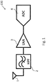
- Fig. 1 depicts a typical direct sampling receiver front-end 100 for a wideband receiver operating for example in the 6 to 8.5 GHz band.
- Antenna 1 receives a RF signal and passes it to high-pass filter 2 which rejects signals below about 6 GHz, with a high rejection notch at around 5.1 to 5.8 GHz (although it will be appreciated that these numbers are provided purely by way of example).
- the output of high-pass filter 2 feeds to the input of low-noise amplifier 3 which provides gain for the signal of interest across the operating band of 6 to 8.5 GHz.
- the output of low-noise amplifier 3 is then fed to an analogue-to-digital converter (ADC) 4 that finally digitises the RF signal.
- ADC analogue-to-digital converter
- Fig. 2 shows a high-pass filter 200.
- the filter shown in Fig. 2 is not in accordance with the claimed invention.
- the passive filter core 210 is depicted as a single-ended filter, operating on a signal part (signal path) RF i .
- the passive filter core 210 is a fifth-order elliptic LC ladder filter with a resonant circuit 211 as one of its reactive elements.
- the other four reactive elements are capacitor C 1 , inductor L 2 , inductor L 3 and capacitor C 2 .
- the resonant circuit 211 comprises an inductor L 1 and a capacitor C 3 in parallel.
- the capacitor C 3 of resonant circuit 211 is connected between nodes A and B. As can be seen in Fig. 2 , nodes A and B are both connected to ac ground nodes. Node A is connected through inductor L 2 and node B is connected through inductor L 3 . The signal passing from RF i to RF o is in phase at nodes A and B.
- the active block 220 is a single-ended to differential Q-boosting circuit that enhances the Q of the inductive components (L 1 , L 2 and L 3 ) of the circuit so as to improve the notch rejection of the filter and provide improved (steeper) pass-band and stop-band roll-off.
- the active block 220 has a single-ended input and provides differential output (both inverting and non-inverting outputs).
- the single-ended input is connected to node A on the input side of the resonant circuit 211 so that this node A drives the active block 220.
- the differential outputs (which are out of phase) are connected at nodes A and B (where the signal path is in phase), i.e. either side of the resonant circuit 211.
- Providing the differential outputs either side of the reactive components of the resonant circuit 211 increases the current (and thus the voltage) on one side and decreases it on the other side, thus increasing the voltage drop across the components (and hence the Q of the components), while retaining stability of the circuit.
- the change in current due to the active circuit on one side of the resonant circuit 211 is equal and opposite to the change in current due to the active circuit on the other side of the resonant circuit 211 so that the energy added on one side is removed on the other side, thus providing circuit stability.
- the input of active block 220 could alternatively be driven by node B instead of node A and the differential inputs could be applied the opposite way round (with the inverting output connected at A and the non-inverting output connected at B).
- the Q of an inductor is defined as the ratio of its imaginary to real impedance.
- the active circuit is arranged to increase the ratio of the imaginary part to the real part of the impedance of said inductor.
- the quality factor is also defined as the ratio of the voltage drop appearing across the inductor or capacitor to the supply/bias voltage. An increase in voltage drop seen across the inductor, means an increase in its Q.
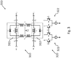
- Fig. 3 shows a high-pass filter 300 according to an embodiment of the invention.
- the circuit 300 is divided into two parts with the upper part being the passive filter core 310 and the lower part being the active circuit 320.
- the passive filter core 310 is depicted as a differential filter, operating on a positive signal part RF i,+ and a negative signal part RF i,- . Although a differential filter is shown and described here, it will be appreciated that half of this circuit can be used as a single-ended filter as shown in Fig. 2 .
- Each half of the passive filter core 310 is a fifth-order elliptic LC ladder filter with a resonant circuit (311 for the positive signal half and 312 for the negative signal half) as one of its reactive elements.
- the other four reactive elements are capacitor C 1 , center-tapped inductor L 2 (or more generally, just an inductor), center-tapped inductor L 3 (or more generally, just an inductor) and capacitor C 2 .
- Each resonant circuit 311, 312 comprises an inductor L 1 and a varactor V 1 in parallel.
- the varactor V 1 is used in place of a more traditional capacitor due to its high Q, capacitance density and robustness with respect to process variations, voltage variations and temperature variations (collectively referred to as PVT variations).
- the varactor V 1 has a tolerance better than or comparable to metal-insulator-metal (MIM) capacitors, but without requiring the more expensive MIM fabrication process.
- Metal-oxide-metal (MOM) capacitors are cheaper to construct than MIM capacitors, but suffer typically +/-15% PVT variation which adversely affects the filter performance on account of variability of notch frequency under PVT variations.
- the varactor V 1 of resonant circuit 311 is connected between nodes A and B. As can be seen in Fig. 3 , nodes A and B are both connected to V DD and are in phase on the signal path. Node A is connected through inductor L 2 and node B is connected through inductor L 3 . As there is no (or insignificantly small) voltage drop across these inductors, both sides of varactor V 1 are held at V DD and therefore there is zero dc bias applied to varactor V 1 . This has the significant advantage of keeping the capacitance of the varactor constant, providing a well-defined capacitance value that is least susceptible to PVT variations.
- the inductors L 2 and L 3 are centre-tapped inductors exploiting mutual coupling in order to reduce chip area.
- L 2 and L 3 are identical components so as to ensure that any voltage losses across them are also identical.
- capacitors C 1 and C 2 dc isolate the filter core and the V DD connection from the antenna input and downstream processing. This is particularly beneficial in relation to the active Q-boosting circuit described further below as C 1 and C 2 guarantee self-biasing (at V DD ) of the differential amplifiers in the active Q-boosting circuit.
- Inductors L 1 in the two resonant circuits can be replaced with a bifilar (transformer) to exploit mutual coupling and further reduce chip area.
- the negative (inverting) signal half of the filter is identical to the positive (non-inverting) signal half described above, except that the varactor V 1 of second resonant circuit 312 is connected between nodes C and D which are connected to V DD through the center-tapped inductors L 2 and L 3 , respectively.
- the active circuit 320 is a Q-boosting circuit that enhances the Q of the inductive components of the circuit so as to improve the notch rejection of the filter and provide improved (steeper) pass-band and stop-band roll-off.
- the active circuit 320 comprises two differential amplifiers.
- a first differential amplifier 321 is connected across the first resonant circuit 311 via nodes A and B.
- the second differential amplifier 322 is connected across the second resonant circuit 312 via nodes C and D.
- First differential amplifier pair 321 comprises amplifying elements M 1 and M 2 (here in the form of MOSFETs, self-biased at V DD to operate in the saturation region).
- the gate of amplifying element M 1 is connected to (and therefore driven by) node A, i.e. the input of the first resonant circuit 311.
- the gate of amplifying element M 2 is connected to (and therefore driven by) node C, i.e. the input of the second resonant circuit 312.
- amplifying elements M 1 and M 2 operate in anti-phase.
- the sources of both amplifying elements M 1 and M 2 are connected together and to current source I 1 which draws current (0.5*I 1 ) through each of the amplifying elements M 1 and M 2 . Any change in the input signals causes one amplifying element to draw more current and the other amplifying element to draw equivalently less current. Accordingly, any current injected at A is drawn off at B and vice versa.
- first differential amplifier 321 an increase in signal voltage at node A is mirrored by a corresponding signal voltage drop at node C.
- the amplification of amplifying element M 1 is increased, resulting in more current draw at node B and a corresponding decrease in voltage at node B.
- the amplification of amplifying element M 2 is reduced, resulting in less current draw at node A and a corresponding increase in voltage at node A.
- the voltage rise at node A is followed by the voltage drop at node B which keeps the circuit operation perfectly stable.
- the voltage rise at A and drop at B causes a large change in the voltage across inductor L 1 , thus greatly increasing the Q of inductor L 1 which in turn produces a marked improvement in the notch rejection of the filter and the pass-band and stop-band roll-off.
- the current change at node A is equal and opposite to the current change at node B.
- second differential amplifier pair 322 is identical, but applied across nodes C and D to cause a corresponding increase in the Q of L 1 of the second resonant circuit 312.
- Fig. 4 shows another embodiment which is similar to the embodiment of Fig. 3 except that in the passive filter core 410 each of the positive and negative signal arms of the differential filter includes an additional resonant circuit.
- a third resonant circuit 413 is formed by putting an inductor L 4 in parallel with the previous dc blocking capacitor C 1 .
- a fourth resonant circuit 414 is formed by putting an inductor L 4 in parallel with the previous dc blocking capacitor C 1 .
- the first differential amplifier 421 and second differential amplifier 422 are identical in operation to the first and second differential amplifiers pairs 421 and 422 of Fig. 3 .
- a third differential amplifier 423 and fourth differential amplifier 424 are provided.
- the third differential amplifier 423 comprises amplifying elements M 5 and M 6 connected together at their sources to third current source I 3 .
- the fourth differential amplifier 424 comprises amplifying elements M 7 and M 8 connected together at their sources to fourth current source I 4 .
- the third differential amplifier 423 is connected across the third resonant circuit 413 at node A and at non-inverting input RF i,+ .
- the gate of M 5 is driven by RF i,+ and the gate of M 6 is driven by RF i,- .
- the fourth differential amplifier 424 is connected across the fourth resonant circuit 414 at node C and at inverting input RF i,- .
- the gate of M 7 is driven by RF i,- and the gate of M 8 is driven by RF i,+ .
- a capacitor e.g., high-Q MIM cap.
- a capacitor can substitute varactor V 1 as shown in Fig. 2 .
- This variation serves to demonstrate that the active circuit may achieve significant gains when a varactor V 1 is not used. This would also apply to the active circuit 320 of Fig. 3 when applied to a passive core 310 with the varactor V 1 replaced with a capacitor.
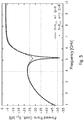
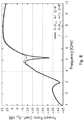
- Fig. 5 shows the filter response (forward transmission coefficient S 21 ) for a particular setup with a single harmonic trap (i.e., one resonant circuit) placing the notch at around 5.1 GHz.
- Two lines are shown on the graph, the line marked with line-points shows the response of the filter with the active circuit switched OFF (effectively achieved simply by turning off the current sources I 1 and I 2 ).
- the solid line shows the response of the filter with the active circuit switched ON.
- the improvement in notch depth and roll-off steepness is readily apparent.
- Q-boosting ON active circuit ON
- Q-boosting ON there is at least 20 dB rejection across the range of about 5 to 5.5 GHz, providing excellent rejection of the IEEE 802.11a wireless LAN band.
- the insertion loss in the pass-band is about 3 dB which is comparable to off the shelf components.
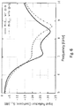
- Fig. 6 shows the input reflection coefficient S 11 of the filter.
- the filter is differentially matched (i.e., S 11 ⁇ -10 dB) to 100 ⁇ over the passband (e.g., 6-8.5 GHz) with Q-boosting (line) enabled and without Q-boosting (line-points).
- Fig. 7 compares the filter responses (S 21 ) for single (line-points) and double harmonic (line) trap elliptic high-pass filters.
- the double harmonic trap filter with two notches shows a steeper pass-band to stop-band roll-off, thus allowing for one notch to be placed closer to the lower edge of the passband with > 20 dB rejection at around IEEE 802.11a.
- Fig. 5 shows the standalone frequency response of the filter.
- the high-pass filter is generally linked to a low-noise amplifier to provide signal gain in the pass-band and out-of-band rejection.
- Fig. 8 shows the response of the combination of the high-pass filter evaluated in Fig. 4 together with a low-noise amplifier. The results are again shown both with and without the active Q-boosting circuit enabled. Without Q-boosting, the signal rejection is > 20 dB at 5.1 GHz (i.e., lower-frequency end of IEEE 802.11a). With Q-boosting enabled, the rejection is > 45 dB at 5.1 GHz. Again the roll-off improves with Q-boosting enabled. Combined with the LNA, the rejection at around 2.4 GHz (IEEE 802.11b/g) is > 50 dB.
Landscapes
- Engineering & Computer Science (AREA)
- Power Engineering (AREA)
- Amplifiers (AREA)
- Networks Using Active Elements (AREA)
Claims (15)
- Differenzschaltung (300) mit einem ersten positiven Arm und einem zweiten negativen Arm; wobei der erste positive Arm mindestens eine erste reaktive Komponente (311) umfasst und der zweite negative Arm mindestens eine zweite reaktive Komponente (312) umfasst;
weiter umfassend:eine aktive Schaltung (320), wobei die aktive Schaltung angeordnet ist, um die Wechselspannungsdifferenz über der ersten reaktiven Komponente (311) durch Ändern des Stroms an einem Eingang zur ersten reaktiven Komponente und des Stroms an einem Ausgang der ersten reaktiven Komponente um gleiche und entgegengesetzte Beträge zu erhöhen, und die aktive Schaltung (320) angeordnet ist, um die Wechselspannungsdifferenz über der zweiten reaktiven Komponente (312) durch Ändern des Stroms an einem Eingang zur zweiten reaktiven Komponente und des Stroms an einem Ausgang der zweiten reaktiven Komponente um gleiche und entgegengesetzte Beträge zu erhöhen;wobei die aktive Schaltung (320) umfasst:ein erstes Verstärkungselement (M1);ein zweites Verstärkungselement (M2);ein drittes Verstärkungselement (M3);ein viertes Verstärkungselement (M4);eine erste Stromquelle (I1), die angeordnet ist, um Strom durch das erste Verstärkungselement (M1) der aktiven Schaltung von dem Ausgang der ersten reaktiven Komponente (311) zu ziehen, und angeordnet ist, um Strom durch das zweite Verstärkungselement (M2) der aktiven Schaltung vom Eingang der ersten reaktiven Komponente (311) zu ziehen, wobei das erste Verstärkungselement (Mi) von einem Signaleingang zur ersten reaktiven Komponente (311) angesteuert wird und das zweite Verstärkungselement (M2) von einem Signaleingang zur zweiten reaktiven Komponente (312) angesteuert wird; undeine zweite Stromquelle (I2), die angeordnet ist, um Strom durch das dritte Verstärkungselement (M3) der aktiven Schaltung von dem Ausgang der zweiten reaktiven Komponente (312) zu ziehen, und angeordnet ist, um Strom durch das vierte Verstärkungselement (M4) der aktiven Schaltung vom Eingang der zweiten reaktiven Komponente (312) zu ziehen, wobei das dritte Verstärkungselement (M3) vom Signaleingang zur zweiten reaktiven Komponente (312) angesteuert wird und das vierte Verstärkungselement (M4) vom Signaleingang zur ersten reaktiven Komponente (311) angesteuert wird. - Differenzschaltung (300) nach Anspruch 1, weiter umfassend eine dritte reaktive Komponente (L2), die zwischen den Eingang der ersten reaktive Komponente (311) und den Eingang der zweiten reaktiven Komponente (312) verbunden ist; und eine vierte reaktive Komponente (L3), die zwischen dem Ausgang der ersten reaktiven Komponente (311) und dem Ausgang der zweiten reaktiven Komponente (312) verbunden ist.
- Differenzschaltung (300) nach Anspruch 2, wobei die dritte und die vierte reaktive Komponente (L2, L3) mittig abgegriffene Induktoren oder Spartransformatoren sind.
- Differenzschaltung (300) nach Anspruch 3, wobei die Mittenabgriffe der dritten und der vierten reaktiven Komponente (L2, L3) mit demselben Gleichspannungspotential verbunden sind.
- Differenzschaltung (300) nach einem der vorstehenden Ansprüche, wobei die Differenzschaltung (300) eine von Folgendem ist: ein Hochpassfilter, ein Tiefpassfilter oder ein Verstärker.
- Differenzschaltung (300) nach einem der vorstehenden Ansprüche, wobei das erste, zweite, dritte und vierte Verstärkungselement (M1-M4) invertierende Verstärker sind und in einer Konfiguration mit gemeinsamer Quelle angeordnet sind.
- Differenzschaltung (300) nach einem der vorstehenden Ansprüche, wobei das erste, zweite, dritte und vierte Verstärkungselement (M1-M4) FETs sind, die jeweils von der Spannung an ihrem jeweiligen Gate angesteuert werden und deren Quelle mit der jeweiligen Stromquelle verbunden ist.
- Differenzschaltung (300) nach einem der vorstehenden Ansprüche, wobei die erste reaktive Komponente (311) Teil einer ersten Resonanzschaltung ist und wobei die zweite reaktive Komponente (312) Teil einer zweiten Resonanzschaltung ist.
- Differenzschaltung (300) nach Anspruch 8, wobei:die erste Resonanzschaltung (311) aus einer induktiven Komponente parallel zu einem Varaktor gebildet ist; unddie zweite Resonanzschaltung (312) aus einer induktiven Komponente parallel zu einem Varaktor gebildet ist; undwobei die erste Resonanzschaltung (311) zum Empfangen eines positiven Teils des Differenzeingangssignals angeordnet ist und die zweite Resonanzschaltung (312) zum Empfangen eines negativen Teils des Differenzeingangssignals angeordnet ist.
- Differenzschaltung (300) nach einem der vorstehenden Ansprüche, wobei die Differenzschaltung (300) ein elliptischer Filter ist.
- Differenzschaltung (400) nach Anspruch 9 oder 10, weiter umfassend eine dritte Resonanzschaltung (413) in Reihe mit der ersten Resonanzschaltung (411) und eine vierte Resonanzschaltung (414) in Reihe mit der zweiten Resonanzschaltung (412).
- Differenzschaltung (400) nach Anspruch 11, wobei die aktive Schaltung (420) angeordnet ist, um die Wechselspannungsdifferenz über der dritten Resonanzschaltung (413) durch Ändern des Stroms an einem Eingang zur dritten Resonanzschaltung (413) und den Strom an einem Ausgang des dritten Resonanzschaltung (413) um gleiche und entgegengesetzte Beträge zu erhöhen, und die aktive Schaltung (420) angeordnet ist, um die Wechselspannungsdifferenz über der vierten Resonanzschaltung (414) durch Ändern des Stroms an einem Eingang zur vierten Resonanzschaltung (414) und den Strom an einem Ausgang der vierten Resonanzschaltung (414) um gleiche und entgegengesetzte Beträge zu erhöhen.
- Differenzschaltung (400) nach Anspruch 11 oder 12, wobei die aktive Schaltung (420) weiter umfasst:ein fünftes Verstärkungselement (M5);ein sechstes Verstärkungselement (M6);ein siebtes Verstärkungselement (M7);ein achtes Verstärkungselement (M8);eine dritte Stromquelle (I3), die angeordnet ist, um Strom durch das fünfte Verstärkungselement (M5) der aktiven Schaltung von dem Ausgang der dritten Resonanzschaltung (413) zu ziehen, und angeordnet ist, um Strom durch das sechste Verstärkungselement (M6) der aktiven Schaltung vom Eingang der dritten Resonanzschaltung (413) zu ziehen, wobei das fünfte Verstärkungselement (M5) von einem Signaleingang zur dritten Resonanzschaltung (413) angesteuert wird und das sechste Verstärkungselement (M6) von einem Signaleingang zur vierten Resonanzschaltung (414) angesteuert wird; undeine vierte Stromquelle (I4), die angeordnet ist, um Strom durch das siebte Verstärkungselement (M7) der aktiven Schaltung von dem Ausgang der vierten Resonanzschaltung (414) zu ziehen, und angeordnet ist, um Strom durch das achte Verstärkungselement (Mg) der aktiven Schaltung vom Eingang der vierten Resonanzschaltung (414) zu ziehen, wobei das siebte Verstärkungselement (M7) vom Signaleingang der vierten Resonanzschaltung (414) angesteuert wird und das achte Verstärkungselement (Mg) vom Signaleingang zur dritten Resonanzschaltung (413) angesteuert wird.
- Differenzschaltung (400) nach Anspruch 13, wobei das erste, zweite, dritte, vierte, fünfte, sechste, siebte und achte Verstärkerelement (M5-M8) invertierende Verstärker sind und in einer Konfiguration mit gemeinsamer Quelle angeordnet sind.
- Differenzschaltung (400) nach Anspruch 13 oder 14, wobei der erste, zweite, dritte, vierte, fünfte, sechste, siebte und achte Verstärker (M5-M8) FETs sind, die jeweils von der Spannung an seinem jeweiligen Gate angesteuert werden und deren Quelle mit der jeweiligen Stromquelle verbunden ist.
Applications Claiming Priority (2)
| Application Number | Priority Date | Filing Date | Title |
|---|---|---|---|
| GBGB1614241.6A GB201614241D0 (en) | 2016-08-19 | 2016-08-19 | Filter |
| PCT/GB2017/052444 WO2018033746A1 (en) | 2016-08-19 | 2017-08-17 | Filter |
Publications (2)
| Publication Number | Publication Date |
|---|---|
| EP3501103A1 EP3501103A1 (de) | 2019-06-26 |
| EP3501103B1 true EP3501103B1 (de) | 2021-11-03 |
Family
ID=57045730
Family Applications (1)
| Application Number | Title | Priority Date | Filing Date |
|---|---|---|---|
| EP17757847.3A Active EP3501103B1 (de) | 2016-08-19 | 2017-08-17 | Filter |
Country Status (6)
| Country | Link |
|---|---|
| US (1) | US10855253B2 (de) |
| EP (1) | EP3501103B1 (de) |
| CN (1) | CN109643978B (de) |
| GB (1) | GB201614241D0 (de) |
| TW (1) | TWI752998B (de) |
| WO (1) | WO2018033746A1 (de) |
Families Citing this family (3)
| Publication number | Priority date | Publication date | Assignee | Title |
|---|---|---|---|---|
| GB2598594A (en) | 2020-09-03 | 2022-03-09 | Novelda As | Filter |
| CN113114165B (zh) * | 2021-03-25 | 2022-07-05 | 中国电子科技集团公司第三十研究所 | 基于带通相位相消的级联多陷波超宽带滤波电路 |
| US11791792B1 (en) * | 2022-04-19 | 2023-10-17 | Apple Inc. | High-order passive filter with capacitive inner tapping technique |
Family Cites Families (21)
| Publication number | Priority date | Publication date | Assignee | Title |
|---|---|---|---|---|
| US4459571A (en) * | 1982-12-20 | 1984-07-10 | Motorola, Inc. | Varactor-tuned helical resonator filter |
| US5451915A (en) * | 1993-05-26 | 1995-09-19 | Hittite Microwave Corporation | Active filter resonator and system and negative resistance generator usable therein |
| US5663690A (en) | 1996-03-06 | 1997-09-02 | Motorola, Inc. | Constant high Q voltage controlled oscillator |
| FR2778288B1 (fr) * | 1998-04-29 | 2000-07-13 | Matra Nortel Communications | Filtre passe-bande accordable |
| US6271716B1 (en) * | 1998-10-30 | 2001-08-07 | Sony Electronics, Inc. | Rcb cancellation in low-side low power supply current sources |
| KR20010080727A (ko) * | 1998-12-11 | 2001-08-22 | 추후기재 | 동조가능 필터 |
| US6600252B2 (en) * | 1999-01-14 | 2003-07-29 | The Regents Of The University Of Michigan | Method and subsystem for processing signals utilizing a plurality of vibrating micromechanical devices |
| HK1049926B (zh) * | 1999-09-01 | 2005-12-23 | 高通股份有限公司 | 具有良好抗擾性的寬頻帶壓控振盪器 |
| US6944435B2 (en) * | 2002-06-03 | 2005-09-13 | Broadcom, Corp. | Unconditionally stable on-chip filter and applications thereof |
| US6990327B2 (en) * | 2003-04-30 | 2006-01-24 | Agency For Science Technology And Research | Wideband monolithic tunable high-Q notch filter for image rejection in RF application |
| WO2005060043A2 (en) | 2003-12-11 | 2005-06-30 | University Of Washington Techtransfer Invention Licensing | Phase shifters, such as for a multiple antenna wireless communication system |
| US20060017515A1 (en) | 2004-07-22 | 2006-01-26 | Columbia University | CMOS negative resistance/Q enhancement method and apparatus |
| TWI326934B (en) | 2006-03-24 | 2010-07-01 | Univ Nat Taiwan | Active bandpass filter |
| US7509102B2 (en) * | 2006-04-07 | 2009-03-24 | Broadcom Corporation | DAC based switching power amplifier |
| US7885629B2 (en) * | 2006-08-03 | 2011-02-08 | Broadcom Corporation | Circuit with Q-enhancement cell having programmable bias current slope |
| US8237509B2 (en) * | 2007-02-23 | 2012-08-07 | Qualcomm, Incorporated | Amplifier with integrated filter |
| JP2011130083A (ja) * | 2009-12-16 | 2011-06-30 | Mitsubishi Electric Corp | 可変フィルタ |
| CN102064787B (zh) * | 2010-12-29 | 2014-05-21 | 海能达通信股份有限公司 | 一种射频带通滤波电路 |
| JP5896718B2 (ja) * | 2011-02-04 | 2016-03-30 | 日本電波工業株式会社 | 圧電発振器 |
| US8497730B1 (en) | 2011-06-09 | 2013-07-30 | Rockwell Collins, Inc. | System for and method of modifying impedance characteristics of circuit elements |
| US8581643B1 (en) * | 2011-10-28 | 2013-11-12 | Lightlab Imaging, Inc. | Phase-lock loop-based clocking system, methods and apparatus |
-
2016
- 2016-08-19 GB GBGB1614241.6A patent/GB201614241D0/en not_active Ceased
-
2017
- 2017-08-16 TW TW106127730A patent/TWI752998B/zh active
- 2017-08-17 US US16/326,471 patent/US10855253B2/en active Active
- 2017-08-17 CN CN201780050673.XA patent/CN109643978B/zh active Active
- 2017-08-17 EP EP17757847.3A patent/EP3501103B1/de active Active
- 2017-08-17 WO PCT/GB2017/052444 patent/WO2018033746A1/en not_active Ceased
Non-Patent Citations (1)
| Title |
|---|
| None * |
Also Published As
| Publication number | Publication date |
|---|---|
| TWI752998B (zh) | 2022-01-21 |
| TW201824743A (zh) | 2018-07-01 |
| GB201614241D0 (en) | 2016-10-05 |
| EP3501103A1 (de) | 2019-06-26 |
| CN109643978B (zh) | 2022-11-08 |
| US20190356303A1 (en) | 2019-11-21 |
| US10855253B2 (en) | 2020-12-01 |
| WO2018033746A1 (en) | 2018-02-22 |
| CN109643978A (zh) | 2019-04-16 |
Similar Documents
| Publication | Publication Date | Title |
|---|---|---|
| US7323939B2 (en) | Low noise amplifier for wideband tunable matching | |
| CN104272583B (zh) | 一种具有尾电流源和基于变压器的振荡回路的电感电容振荡器 | |
| US10305436B2 (en) | Scaleable RF tuned low noise amplifier | |
| US12355428B2 (en) | System and method for integrated filtering and amplification | |
| EP3501103B1 (de) | Filter | |
| Kia | Adaptive CMOS LNA using highly tunable active inductor | |
| Faruqe et al. | Comparative analysis and simulation of active inductors for RF applications in 90 nm CMOS | |
| Reja et al. | A wide frequency range CMOS active inductor for UWB bandpass filters | |
| Manjula et al. | Performance analysis of a low power low noise tunable band pass filter for multiband RF front end | |
| US12451868B2 (en) | Filter | |
| Reja et al. | A compact CMOS UWB LNA using tunable active inductors for WLAN interference rejection | |
| Elahi et al. | A UWB LNA with interference rejection using enhanced-Q active inductor | |
| Chen et al. | Process Variation Aware Wide Tuning Band Pass Filter for Steep Roll‐Off High Rejection | |
| Halkhams et al. | Fully differential active inductor for CMOS active filter applications | |
| Božanić et al. | Broadband Low-Noise Amplifiers | |
| GB2541782A (en) | Scaleable RF tuned low noise amplifier | |
| Worapishet et al. | Enhanced tuneable coupled inductor for ultra-wide variable centre frequency LC filters | |
| Chitranshi et al. | Bandwidth Extension of Constant-Q Bandpass Filter using Bandwidth Extension Techniques |
Legal Events
| Date | Code | Title | Description |
|---|---|---|---|
| STAA | Information on the status of an ep patent application or granted ep patent |
Free format text: STATUS: UNKNOWN |
|
| STAA | Information on the status of an ep patent application or granted ep patent |
Free format text: STATUS: THE INTERNATIONAL PUBLICATION HAS BEEN MADE |
|
| PUAI | Public reference made under article 153(3) epc to a published international application that has entered the european phase |
Free format text: ORIGINAL CODE: 0009012 |
|
| STAA | Information on the status of an ep patent application or granted ep patent |
Free format text: STATUS: REQUEST FOR EXAMINATION WAS MADE |
|
| 17P | Request for examination filed |
Effective date: 20190314 |
|
| AK | Designated contracting states |
Kind code of ref document: A1 Designated state(s): AL AT BE BG CH CY CZ DE DK EE ES FI FR GB GR HR HU IE IS IT LI LT LU LV MC MK MT NL NO PL PT RO RS SE SI SK SM TR |
|
| AX | Request for extension of the european patent |
Extension state: BA ME |
|
| DAV | Request for validation of the european patent (deleted) | ||
| DAX | Request for extension of the european patent (deleted) | ||
| GRAP | Despatch of communication of intention to grant a patent |
Free format text: ORIGINAL CODE: EPIDOSNIGR1 |
|
| STAA | Information on the status of an ep patent application or granted ep patent |
Free format text: STATUS: GRANT OF PATENT IS INTENDED |
|
| RIC1 | Information provided on ipc code assigned before grant |
Ipc: H03H 11/52 20060101ALI20201030BHEP Ipc: H03H 11/06 20060101ALI20201030BHEP Ipc: H03H 7/03 20060101ALI20201030BHEP Ipc: H03H 7/01 20060101AFI20201030BHEP |
|
| INTG | Intention to grant announced |
Effective date: 20201119 |
|
| GRAJ | Information related to disapproval of communication of intention to grant by the applicant or resumption of examination proceedings by the epo deleted |
Free format text: ORIGINAL CODE: EPIDOSDIGR1 |
|
| STAA | Information on the status of an ep patent application or granted ep patent |
Free format text: STATUS: REQUEST FOR EXAMINATION WAS MADE |
|
| INTC | Intention to grant announced (deleted) | ||
| GRAP | Despatch of communication of intention to grant a patent |
Free format text: ORIGINAL CODE: EPIDOSNIGR1 |
|
| STAA | Information on the status of an ep patent application or granted ep patent |
Free format text: STATUS: GRANT OF PATENT IS INTENDED |
|
| INTG | Intention to grant announced |
Effective date: 20210519 |
|
| GRAS | Grant fee paid |
Free format text: ORIGINAL CODE: EPIDOSNIGR3 |
|
| GRAA | (expected) grant |
Free format text: ORIGINAL CODE: 0009210 |
|
| STAA | Information on the status of an ep patent application or granted ep patent |
Free format text: STATUS: THE PATENT HAS BEEN GRANTED |
|
| AK | Designated contracting states |
Kind code of ref document: B1 Designated state(s): AL AT BE BG CH CY CZ DE DK EE ES FI FR GB GR HR HU IE IS IT LI LT LU LV MC MK MT NL NO PL PT RO RS SE SI SK SM TR |
|
| REG | Reference to a national code |
Ref country code: GB Ref legal event code: FG4D |
|
| REG | Reference to a national code |
Ref country code: AT Ref legal event code: REF Ref document number: 1444902 Country of ref document: AT Kind code of ref document: T Effective date: 20211115 Ref country code: CH Ref legal event code: EP |
|
| REG | Reference to a national code |
Ref country code: IE Ref legal event code: FG4D |
|
| REG | Reference to a national code |
Ref country code: DE Ref legal event code: R096 Ref document number: 602017048730 Country of ref document: DE |
|
| REG | Reference to a national code |
Ref country code: LT Ref legal event code: MG9D |
|
| REG | Reference to a national code |
Ref country code: NL Ref legal event code: MP Effective date: 20211103 |
|
| REG | Reference to a national code |
Ref country code: AT Ref legal event code: MK05 Ref document number: 1444902 Country of ref document: AT Kind code of ref document: T Effective date: 20211103 |
|
| PG25 | Lapsed in a contracting state [announced via postgrant information from national office to epo] |
Ref country code: RS Free format text: LAPSE BECAUSE OF FAILURE TO SUBMIT A TRANSLATION OF THE DESCRIPTION OR TO PAY THE FEE WITHIN THE PRESCRIBED TIME-LIMIT Effective date: 20211103 Ref country code: LT Free format text: LAPSE BECAUSE OF FAILURE TO SUBMIT A TRANSLATION OF THE DESCRIPTION OR TO PAY THE FEE WITHIN THE PRESCRIBED TIME-LIMIT Effective date: 20211103 Ref country code: FI Free format text: LAPSE BECAUSE OF FAILURE TO SUBMIT A TRANSLATION OF THE DESCRIPTION OR TO PAY THE FEE WITHIN THE PRESCRIBED TIME-LIMIT Effective date: 20211103 Ref country code: BG Free format text: LAPSE BECAUSE OF FAILURE TO SUBMIT A TRANSLATION OF THE DESCRIPTION OR TO PAY THE FEE WITHIN THE PRESCRIBED TIME-LIMIT Effective date: 20220203 Ref country code: AT Free format text: LAPSE BECAUSE OF FAILURE TO SUBMIT A TRANSLATION OF THE DESCRIPTION OR TO PAY THE FEE WITHIN THE PRESCRIBED TIME-LIMIT Effective date: 20211103 |
|
| PG25 | Lapsed in a contracting state [announced via postgrant information from national office to epo] |
Ref country code: IS Free format text: LAPSE BECAUSE OF FAILURE TO SUBMIT A TRANSLATION OF THE DESCRIPTION OR TO PAY THE FEE WITHIN THE PRESCRIBED TIME-LIMIT Effective date: 20220303 Ref country code: SE Free format text: LAPSE BECAUSE OF FAILURE TO SUBMIT A TRANSLATION OF THE DESCRIPTION OR TO PAY THE FEE WITHIN THE PRESCRIBED TIME-LIMIT Effective date: 20211103 Ref country code: PT Free format text: LAPSE BECAUSE OF FAILURE TO SUBMIT A TRANSLATION OF THE DESCRIPTION OR TO PAY THE FEE WITHIN THE PRESCRIBED TIME-LIMIT Effective date: 20220303 Ref country code: PL Free format text: LAPSE BECAUSE OF FAILURE TO SUBMIT A TRANSLATION OF THE DESCRIPTION OR TO PAY THE FEE WITHIN THE PRESCRIBED TIME-LIMIT Effective date: 20211103 Ref country code: NO Free format text: LAPSE BECAUSE OF FAILURE TO SUBMIT A TRANSLATION OF THE DESCRIPTION OR TO PAY THE FEE WITHIN THE PRESCRIBED TIME-LIMIT Effective date: 20220203 Ref country code: NL Free format text: LAPSE BECAUSE OF FAILURE TO SUBMIT A TRANSLATION OF THE DESCRIPTION OR TO PAY THE FEE WITHIN THE PRESCRIBED TIME-LIMIT Effective date: 20211103 Ref country code: LV Free format text: LAPSE BECAUSE OF FAILURE TO SUBMIT A TRANSLATION OF THE DESCRIPTION OR TO PAY THE FEE WITHIN THE PRESCRIBED TIME-LIMIT Effective date: 20211103 Ref country code: HR Free format text: LAPSE BECAUSE OF FAILURE TO SUBMIT A TRANSLATION OF THE DESCRIPTION OR TO PAY THE FEE WITHIN THE PRESCRIBED TIME-LIMIT Effective date: 20211103 Ref country code: GR Free format text: LAPSE BECAUSE OF FAILURE TO SUBMIT A TRANSLATION OF THE DESCRIPTION OR TO PAY THE FEE WITHIN THE PRESCRIBED TIME-LIMIT Effective date: 20220204 Ref country code: ES Free format text: LAPSE BECAUSE OF FAILURE TO SUBMIT A TRANSLATION OF THE DESCRIPTION OR TO PAY THE FEE WITHIN THE PRESCRIBED TIME-LIMIT Effective date: 20211103 |
|
| PG25 | Lapsed in a contracting state [announced via postgrant information from national office to epo] |
Ref country code: SM Free format text: LAPSE BECAUSE OF FAILURE TO SUBMIT A TRANSLATION OF THE DESCRIPTION OR TO PAY THE FEE WITHIN THE PRESCRIBED TIME-LIMIT Effective date: 20211103 Ref country code: SK Free format text: LAPSE BECAUSE OF FAILURE TO SUBMIT A TRANSLATION OF THE DESCRIPTION OR TO PAY THE FEE WITHIN THE PRESCRIBED TIME-LIMIT Effective date: 20211103 Ref country code: RO Free format text: LAPSE BECAUSE OF FAILURE TO SUBMIT A TRANSLATION OF THE DESCRIPTION OR TO PAY THE FEE WITHIN THE PRESCRIBED TIME-LIMIT Effective date: 20211103 Ref country code: EE Free format text: LAPSE BECAUSE OF FAILURE TO SUBMIT A TRANSLATION OF THE DESCRIPTION OR TO PAY THE FEE WITHIN THE PRESCRIBED TIME-LIMIT Effective date: 20211103 Ref country code: DK Free format text: LAPSE BECAUSE OF FAILURE TO SUBMIT A TRANSLATION OF THE DESCRIPTION OR TO PAY THE FEE WITHIN THE PRESCRIBED TIME-LIMIT Effective date: 20211103 Ref country code: CZ Free format text: LAPSE BECAUSE OF FAILURE TO SUBMIT A TRANSLATION OF THE DESCRIPTION OR TO PAY THE FEE WITHIN THE PRESCRIBED TIME-LIMIT Effective date: 20211103 |
|
| REG | Reference to a national code |
Ref country code: DE Ref legal event code: R097 Ref document number: 602017048730 Country of ref document: DE |
|
| PLBE | No opposition filed within time limit |
Free format text: ORIGINAL CODE: 0009261 |
|
| STAA | Information on the status of an ep patent application or granted ep patent |
Free format text: STATUS: NO OPPOSITION FILED WITHIN TIME LIMIT |
|
| 26N | No opposition filed |
Effective date: 20220804 |
|
| PG25 | Lapsed in a contracting state [announced via postgrant information from national office to epo] |
Ref country code: AL Free format text: LAPSE BECAUSE OF FAILURE TO SUBMIT A TRANSLATION OF THE DESCRIPTION OR TO PAY THE FEE WITHIN THE PRESCRIBED TIME-LIMIT Effective date: 20211103 |
|
| PG25 | Lapsed in a contracting state [announced via postgrant information from national office to epo] |
Ref country code: SI Free format text: LAPSE BECAUSE OF FAILURE TO SUBMIT A TRANSLATION OF THE DESCRIPTION OR TO PAY THE FEE WITHIN THE PRESCRIBED TIME-LIMIT Effective date: 20211103 |
|
| PG25 | Lapsed in a contracting state [announced via postgrant information from national office to epo] |
Ref country code: MC Free format text: LAPSE BECAUSE OF FAILURE TO SUBMIT A TRANSLATION OF THE DESCRIPTION OR TO PAY THE FEE WITHIN THE PRESCRIBED TIME-LIMIT Effective date: 20211103 |
|
| REG | Reference to a national code |
Ref country code: CH Ref legal event code: PL |
|
| PG25 | Lapsed in a contracting state [announced via postgrant information from national office to epo] |
Ref country code: LU Free format text: LAPSE BECAUSE OF NON-PAYMENT OF DUE FEES Effective date: 20220817 Ref country code: LI Free format text: LAPSE BECAUSE OF NON-PAYMENT OF DUE FEES Effective date: 20220831 Ref country code: CH Free format text: LAPSE BECAUSE OF NON-PAYMENT OF DUE FEES Effective date: 20220831 |
|
| REG | Reference to a national code |
Ref country code: BE Ref legal event code: MM Effective date: 20220831 |
|
| PG25 | Lapsed in a contracting state [announced via postgrant information from national office to epo] |
Ref country code: IT Free format text: LAPSE BECAUSE OF FAILURE TO SUBMIT A TRANSLATION OF THE DESCRIPTION OR TO PAY THE FEE WITHIN THE PRESCRIBED TIME-LIMIT Effective date: 20211103 |
|
| P01 | Opt-out of the competence of the unified patent court (upc) registered |
Effective date: 20230513 |
|
| PG25 | Lapsed in a contracting state [announced via postgrant information from national office to epo] |
Ref country code: IE Free format text: LAPSE BECAUSE OF NON-PAYMENT OF DUE FEES Effective date: 20220817 |
|
| PG25 | Lapsed in a contracting state [announced via postgrant information from national office to epo] |
Ref country code: BE Free format text: LAPSE BECAUSE OF NON-PAYMENT OF DUE FEES Effective date: 20220831 |
|
| PG25 | Lapsed in a contracting state [announced via postgrant information from national office to epo] |
Ref country code: HU Free format text: LAPSE BECAUSE OF FAILURE TO SUBMIT A TRANSLATION OF THE DESCRIPTION OR TO PAY THE FEE WITHIN THE PRESCRIBED TIME-LIMIT; INVALID AB INITIO Effective date: 20170817 |
|
| PG25 | Lapsed in a contracting state [announced via postgrant information from national office to epo] |
Ref country code: CY Free format text: LAPSE BECAUSE OF FAILURE TO SUBMIT A TRANSLATION OF THE DESCRIPTION OR TO PAY THE FEE WITHIN THE PRESCRIBED TIME-LIMIT Effective date: 20211103 |
|
| PG25 | Lapsed in a contracting state [announced via postgrant information from national office to epo] |
Ref country code: MK Free format text: LAPSE BECAUSE OF FAILURE TO SUBMIT A TRANSLATION OF THE DESCRIPTION OR TO PAY THE FEE WITHIN THE PRESCRIBED TIME-LIMIT Effective date: 20211103 |
|
| PG25 | Lapsed in a contracting state [announced via postgrant information from national office to epo] |
Ref country code: MT Free format text: LAPSE BECAUSE OF FAILURE TO SUBMIT A TRANSLATION OF THE DESCRIPTION OR TO PAY THE FEE WITHIN THE PRESCRIBED TIME-LIMIT Effective date: 20211103 |
|
| PGFP | Annual fee paid to national office [announced via postgrant information from national office to epo] |
Ref country code: DE Payment date: 20250917 Year of fee payment: 9 |
|
| PGFP | Annual fee paid to national office [announced via postgrant information from national office to epo] |
Ref country code: GB Payment date: 20250916 Year of fee payment: 9 |
|
| PGFP | Annual fee paid to national office [announced via postgrant information from national office to epo] |
Ref country code: FR Payment date: 20250917 Year of fee payment: 9 |
|
| PG25 | Lapsed in a contracting state [announced via postgrant information from national office to epo] |
Ref country code: TR Free format text: LAPSE BECAUSE OF FAILURE TO SUBMIT A TRANSLATION OF THE DESCRIPTION OR TO PAY THE FEE WITHIN THE PRESCRIBED TIME-LIMIT Effective date: 20211103 |