EP3500865B1 - Optical rf spectrum analyser - Google Patents
Optical rf spectrum analyser Download PDFInfo
- Publication number
- EP3500865B1 EP3500865B1 EP17842446.1A EP17842446A EP3500865B1 EP 3500865 B1 EP3500865 B1 EP 3500865B1 EP 17842446 A EP17842446 A EP 17842446A EP 3500865 B1 EP3500865 B1 EP 3500865B1
- Authority
- EP
- European Patent Office
- Prior art keywords
- signal
- frequency
- over time
- optical
- spectral weight
- Prior art date
- Legal status (The legal status is an assumption and is not a legal conclusion. Google has not performed a legal analysis and makes no representation as to the accuracy of the status listed.)
- Active
Links
- 230000003287 optical effect Effects 0.000 title claims description 126
- 238000001228 spectrum Methods 0.000 title claims description 68
- 230000003595 spectral effect Effects 0.000 claims description 95
- 238000000034 method Methods 0.000 claims description 23
- 238000011084 recovery Methods 0.000 claims description 23
- 230000008859 change Effects 0.000 claims description 8
- 230000008878 coupling Effects 0.000 claims description 3
- 238000010168 coupling process Methods 0.000 claims description 3
- 238000005859 coupling reaction Methods 0.000 claims description 3
- 230000001419 dependent effect Effects 0.000 claims description 3
- 230000006870 function Effects 0.000 description 30
- 238000005259 measurement Methods 0.000 description 15
- 238000010183 spectrum analysis Methods 0.000 description 10
- 238000010586 diagram Methods 0.000 description 7
- 238000005516 engineering process Methods 0.000 description 5
- 238000012545 processing Methods 0.000 description 5
- 238000010408 sweeping Methods 0.000 description 5
- 230000000694 effects Effects 0.000 description 4
- 238000004519 manufacturing process Methods 0.000 description 4
- 238000013507 mapping Methods 0.000 description 4
- 230000004044 response Effects 0.000 description 4
- 238000004458 analytical method Methods 0.000 description 3
- 238000002474 experimental method Methods 0.000 description 3
- XUIMIQQOPSSXEZ-UHFFFAOYSA-N Silicon Chemical group [Si] XUIMIQQOPSSXEZ-UHFFFAOYSA-N 0.000 description 2
- 238000013459 approach Methods 0.000 description 2
- 230000008901 benefit Effects 0.000 description 2
- 238000013461 design Methods 0.000 description 2
- 238000001914 filtration Methods 0.000 description 2
- 230000010354 integration Effects 0.000 description 2
- 230000008569 process Effects 0.000 description 2
- 239000007787 solid Substances 0.000 description 2
- 230000001427 coherent effect Effects 0.000 description 1
- 210000001520 comb Anatomy 0.000 description 1
- 238000011161 development Methods 0.000 description 1
- 230000018109 developmental process Effects 0.000 description 1
- 239000006185 dispersion Substances 0.000 description 1
- 239000000835 fiber Substances 0.000 description 1
- 238000001000 micrograph Methods 0.000 description 1
- 238000012544 monitoring process Methods 0.000 description 1
- 229910052710 silicon Inorganic materials 0.000 description 1
- 239000010703 silicon Substances 0.000 description 1
- 238000012360 testing method Methods 0.000 description 1
- 230000000699 topical effect Effects 0.000 description 1
- 230000009466 transformation Effects 0.000 description 1
Images


Classifications
-
- G—PHYSICS
- G01—MEASURING; TESTING
- G01R—MEASURING ELECTRIC VARIABLES; MEASURING MAGNETIC VARIABLES
- G01R23/00—Arrangements for measuring frequencies; Arrangements for analysing frequency spectra
- G01R23/16—Spectrum analysis; Fourier analysis
- G01R23/17—Spectrum analysis; Fourier analysis with optical or acoustical auxiliary devices
Definitions
- This disclosure relates to optical RF spectrum analysers and methods for analysing an input RF signal.
- RF measurement resolution is solely dependent on the optical filtering bandwidth. For example, in order to have an RF measurement resolution of 20MHz, it requires a highly selective optical filter with a 3dB bandwidth of 20MHz, which is extremely complex or even not possible to be achieved in optical fabrication.
- An optical RF spectrum analyser comprises:
- the signal recovery module may be configured to perform a deconvolution of the RF signal over time based on the spectral weight function.
- the deconvolution may be based on an analytical approximation of the spectral weight function.
- the signal recovery module may be configured to perform the deconvolution of the RF signal over time by using a waveform of the RF signal over time as a frequency domain signal.
- Using the waveform of the RF signal over time as a frequency domain signal may comprise creating a frequency axis associated with the RF signal over time based on a rate of modifying the frequency relationship between the spectral weight function and the carrier frequency over time.
- the spectral weight may be a resonance.
- the resonance may be a ring oscillator.
- the optical modulator may comprise a laser source to generate a laser at the carrier frequency.
- the frequency control module may be to modify the relationship between the spectral weight function and the carrier frequency by varying the carrier frequency. Varying the carrier frequency may comprise performing a sweep across a frequency range.
- Modifying the relationship between the spectral weight function and the carrier frequency over time may be based on a rate of change per unit time and the signal recovery module may be to calculate the RF spectrum based on the rate of change.
- a method for analysing an input RF signal comprises:
- Calculating the spectrum of the input RF signal may comprise performing a deconvolution of the RF signal over time based on the spectral weight function.
- the deconvolution may be based on an analytical approximation of the spectral weight function.
- Performing the deconvolution of the RF signal over time may comprise using a waveform of the RF signal over time as a frequency domain signal.
- Using the waveform of the RF signal over time as a frequency domain signal may comprise creating a frequency axis associated with the RF signal over time based on a rate of modifying the frequency relationship between the spectral weight function and the carrier frequency over time.
- Modifying the relationship between the spectral weight function and the carrier frequency may comprise varying a carrier frequency of a laser source.
- Varying the carrier frequency may comprise performing a sweep across a frequency range.
- Modifying the relationship between the spectral weight function and the carrier frequency over time may be based on a rate of change per unit time and calculating the RF spectrum is based on the rate of change.
- a method for controlling an RF signal analyser comprising:
- This disclosure provides a technology that breaks the one-to-one relationship between RF measurement resolution and optical bandwidth, provides a high RF measurement resolution without increasing the design and manufacture complexity, recovers both amplitude and frequency information of the microwave signals and enables the on-chip RF frequency measurement system.
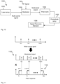
- Fig. 1 illustrates an optical RF spectrum analyser 100 comprising a signal input 101, a modulator 102, frequency control 103, spectral weight 104, such as a filter, optical field integrator 105 and signal recovery module 106.
- Fig. 2 illustrates a method 200 for RF spectrum analysis
- Fig. 3 illustrates a signal flow 300 for RF spectrum analysis.
- the reference numerals in Figs. 1, 2 and 3 correspond to each other in the sense reference numerals 101, 201 and 301 correspond to each other.
- signal input 101 receives 201 an input signal 301
- modulator 102 creates 202 a modulated signal 302 with optical sidebands.
- Frequency control 103 maps 203 the frequency signal 302 into a time domain 303 and spectral weight 104 applies 204 a spectral weight 304 to the time domain signal.
- the frequency integrator 105 integrates 205 the signal to create an integrated time signal 305 and the signal recovery module 106 recovers 206 the signal to calculate the RF spectrum of the input signal 301.
- the input 101 may be an antenna that receives a spectrally limited (narrowband) input signal.
- the narrow band signal is shown at 310.
- the narrow band signal 310 is symmetrical around centre frequency 311.
- the middle of narrow band signal 310 is spaced apart from the origin of the frequency axis by the centre frequency 311. It is noted, however, that the input signal can have any spectrum and in most cases, the input spectrum is unknown.
- the modulation in step 202 by modulator 102 generates an upper sideband 320 and a lower sideband 321.
- the centre of the upper sideband 320 and the lower sideband 321 are spaced apart from a modulator frequency 322 by the centre frequency 311.
- the centre frequency 311 may be the optical frequency of a laser. Since optical frequencies are by magnitudes higher than radio frequencies the frequency axis is broken in Fig. 3 .
- An example RF centre frequency 311 may be 20 GHz and an example optical frequency of carrier 322 may be 195 THz.
- the frequency control 103 maps 203 the modulated signal 302 into the time domain by sweeping the carrier frequency 322 from a low optical wavelength to a high optical wavelength, such as from 1546.45 nm to 1547.25 nm. In effect, this shifts the sidebands 320, 321 as well as the carrier 322 rightwards over time as indicated by time arrow 303.
- the sweep rate is 10 MHz per 1 ms.
- integrator 105 such as a photodiode
- a spectral weight 104 is applied to the signal.
- the spectral weight may be an optical resonance and an example frequency response is plotted at 304 in Fig. 3 .
- Applying a spectral weight basically means multiplying the frequency spectrum 302 at each frequency with the spectral weight 304 at that frequency and then integrating across the entire frequency range. This is also referred to as convolution in the time domain, which becomes the multiplication in the frequency domain.
- the integrated time signal 305 falls back towards zero until the carrier 322 move across the spectral weight 304 resulting in a second peak 352.
- the lower sideband moving across the spectral weight 304 results in a third peak 353.
- the overlapping of spectra may be described as a frequency relationship between the spectral weight function 304 and the carrier frequency 322.
- the frequency relationship is defined by the spectral weight in the sense that the spectral weight defines the relative positioning or alignment between the carrier frequency 322 and the spectral weight function 304.
- This may comprise a fixed spectral weight function, such as implemented by an fixed optical ring oscillator.
- the spectral weight may be tuneable such as by tuning the optical ring oscillator or by using an optical processor. Regardless of the tuning, the spectral weight defines a frequency relationship between the carrier frequency 322 and the spectral weight function 304.
- a particular spectral relationship may be that the spectral weight function is located at a significantly higher frequency than the carrier, is located 10 GHz above the carrier or is located above the carrier by more than the upper sideband 320 frequency.
- Modifying the frequency relationship over time may comprise the above mentioned sweep and causes the overlap as described above.
- the three peaks 351, 352 and 353 are clearly separated as shown in integrated time signal 305 in Fig. 3 .
- the recovery module 106 can detect the three peaks 351, 352 and 353 as the local maxima and measure the time t 0 354 between the upper sideband peak 351 and the carrier peak 352.
- This time t 0 354 is indicative of the time between the overlap of the upper sideband 320 over the spectral weight 304 and the carrier 322 over the spectral weight.
- the time t 0 is indicative of the time period during which the modulated signal spectrum was shifted by f 0 .
- the recovery module 106 can apply a deconvolution algorithm to the time signal. It is noted that many processes in signal processing are described by a convolution of two time signals, such as an input signal and a filter response, which can be transformed into a multiplication in frequency space. In contrast, here the convolution occurs in frequency space between the modulated signal 302 and the spectral weight spectrum 304 but the output is a time domain integrated time signal 305. However, it is possible to replace the time axis of the integrated time signal 305 by a frequency axis according to the sweep rate.
- the recovery module can multiply the time values on the time axis of integrated time signal 305 by 10 MHz/s to convert them to frequencies and apply an offset if applicable.
- the waveform of the integrated time signal 305 can then be passed as a frequency domain signal using the determined frequency axis to a deconvolution algorithm in order to calculate an estimate of the original signal 302.
- the deconvolution may be performed by a processor of a computing system, such as by executing Python code from the scipy.signal.deconvolve package.
- an FPGA performs the deconvolution.
- the accuracy of the deconvolution result can be increased by using the actual spectrum of the spectral weight 204 or an approximation thereof.
- One approximation may be a Gaussian distribution.
- a more accurate approximation may be a Dirac impulse.
- the spectrum analysis system can be realized via 5 signal processing steps in both optical and electrical domain, which include optical sideband (OSB) generation, frequency-to-time mapping, spectral weighting, optical field integration and signal recovery.
- OSB optical sideband
- the input RF signal is applied onto the optical carrier generated by an optical source via an electro-optic modulation, hence realizing the optical sideband generation.
- the optical sideband information in the optical spectrum is translated into a waveform in time domain via frequency-to-time domain mapping where its intensity profile becomes a scaled replica of its optical spectrum.
- the time-varying waveform is transmitted through a spectral weight module, such as an optical filter, where its intensity at the output at each time instance is weighted according to the contributing frequency component.
- an optical field integrator such as photodetector or optical powermeter is employed to measure the exact light intensity at each time instance.
- a signal recovery module based on the deconvolution theorem is used to reconstruct the input RF signal spectrum from the light intensity measured by the optical field integrator.
- the sweeping range can be further extended, e.g. C+L band.
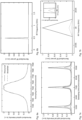
- the optical filter 404 to provide spectral weighting in the system 400 is based on a single ring resonator centered at 1546.85 nm with a 3dB bandwidth of about 1.4 GHz. The measured optical spectrum of the filter is shown in Fig. 5a .
- Fig. 5c shows the measured light intensity waveform at the output of optical field integrator 405 which was an optical power meter in the experiment.
- the results shows the mapping of optical power intensity onto the time domain, the effect of OSB generation 402 and the weighting of optical intensities.
- the estimated frequency of the RF signal at the output of the signal recovery module 406 is shown in Fig. 5d .
- the recovery of the input signal is done through an inverse transformation via various existing signal deconvolution algorithms. For example, the blind deconvolution methods for image and audio processing applications can be adapted and used in the recovery module.
- the measurement error is less than 25MHz which is much less than the filter bandwidth of 1.4GHz.
- Figs. 6a and 6b depict the measurement when the input microwave frequency is reduced to 0.5 GHz which is much smaller than the 3dB bandwidth of the optical filter. Although the output light intensity of the optical power meter is broadened to a single peak as can be seen from Fig. 6a , the frequency of the RF signal can be accurately identified via the new technology as shown in Fig. 6b .
- Fig. 7a and Fig. 7b respectively show the measured light intensity waveform and the estimated modulated signal when the input RF frequency was fixed at 20 GHz and its power was varied. As can be seen, the technology successfully recovers both the amplitude and frequency of the signal.
- the estimated amplitude errors are 0.72, 0.126 and 0.06 dB at 0dBm, -10dBm and -20 dBm input RF power respectively.
- Combining the frequency-to-time mapping module and the spectral weight module with the optical field integrator and a signal recovery module enables the reconstruction of input RF signal spectra with high resolution and also significantly reduces the design and manufacture complexity.
- This technology improves the measurement resolution and operating bandwidth and breaks the one-to-one relationship between RF measurement resolution and optical bandwidth, recovers both amplitude and frequency information of the microwave signals and also enables the on-chip RF frequency measurement system.
- the proposed solution to microwave frequency measurement is insensitive to the wavelength drifting of the optical source and devices as the optical carrier and sidebands information provide self-reference functions.
- the deconvolution may be performed by a processor of a computer system, such as recovery module 106.
- This processor may also perform controlling tasks of the spectrum analyser 100, such as under the instructions of software code that is stored on program memory connected to the processor. These controlling tasks may include generating a modulator control signal to control modulation of the input RF signal 101 onto a carrier frequency 322 by optical modulator 102 to modify a relationship between a spectral weight function 304 and the carrier frequency 322 over time. This basically means that there is another connection in Fig. 1 between the recovery module 106 and the frequency control 103.
- the processor further receives the sensed RF signal over time 305 indicative of the modified signal created by the optical spectral weight 104.
- the processor calculates a spectrum of the input RF signal based on the RF signal over time, such as by applying a deconvolution algorithm to the RF signal over time as described above.
- RF signal 801 in Fig. 8 corresponds to RF signal 101 in Fig. 1 .
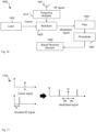
- Fig. 8 shows the schematic diagram of another method for optical RF spectrum analysis, which employs a filter bank 804 to modify the relationship between the spectral weight function 804 and the carrier frequency 803 without varying the carrier frequency 803.
- the modulated optical signal is generated by modulating the RF signal 801 of interest onto the fix-wavelength carrier signal from laser 803. It is then evenly split and sent to a bank of narrow-band optical filters 804 with identical line shapes. Each individual filter is centered at a distinct frequency (f 1 , f 2 ,... f N ) with a constant spacing. It is noted that the relationship between the carrier and the individual filters is changed over time as described before, such as by sweeping the carrier frequency.
- the use of multiple filters as shown in Fig. 8 reduces the time required for the analysis. For example, with four filters only a quarter of the analysis time for one filter is required.
- Fig. 9 shows how each split portion of the modulated signal is multiplied with a shifted spectral weight.
- the weighted spectrum of the modulated signal is then sent to a photodiode 805 where integration over the entire spectrum of modulated signal is implemented.
- the power outputs of the photodiodes are stitched up and deconvolved with the filter line shape, thus the real-time spectrum of the input RF signal is obtained.
- Fig. 10 illustrates another example 1000 of using the filter bank 1004 to realize the optical RF spectrum analyser.
- a laser array 1003 is used to generate multiple carrier signals at different frequencies(fc 1 , fc 2 ,... fc 2N ). Then, the carrier signals are injected to the modulator 1002. RF information is mapped to every carrier signal, hence generating 2N copies of the modulated signal centered at fc 1 , fc 2 ,... fc 2N , respectively. It is then evenly split and sent to a bank of narrow-band optical filters 1004 with identical line shapes.
- each filter output is the product of the shifted spectral weight function and the modulated signal.
- Fig. 11 illustrates the spectra of the optical RF spectrum analyser based on a laser-filter array.
- Fig. 12 shows the schematic diagram of an optical RF spectrum analysis system 1200 based on a laser source 1203 which generates a fixed-wavelength carrier, a modulator 1202, a tunable optical filter 1204, a photodiode 1205 and a signal recovery element 1206.
- the optical filter is of distinct location at each time instance (t 1 , t 2 ,... t N ) as shown in Fig. 13 , a sweep across a frequency range can be achieved.
- Fig. 14 shows another example.
- the laser array 1403 generates multiple carrier signals with a constant frequency spacing (fc 1 , fc 2 ,... fc N ).
- the optical carrier signals are injected to the modulator 1402 to obtain N copies of the modulated optical signal 1401 centered at fc 1 , fc 2 ,... fcrr and then the output of the modulator is sent to a delay element 1410 (e.g. dispersive delay line).
- the time delay provided by the delay element is optical frequency dependent, which indicates each copy of the modulated signal will arrive at the filter 1404 at a different time.
- a dispersive element with a linear delay slope is employed in the system as an optical delay line 1410, it leads to a constant time delay between the n and n+1 (1 ⁇ n ⁇ N) copies of the modulated signal.
- Fig. 15 illustrates the corresponding spectra.
- Fig. 16 illustrates how instead of applying the input RF signal 1601 directly onto the carrier signal generated by the laser source 1603, RF signal 1601 can be sent firstly to a frequency multiplier 1610 then followed by a modulator 1602.
- a frequency doubler could double the input RF frequency as shown in Fig. 17 , thus the relative spacing between the carrier signal and the sidebands is also increased by a factor of 2 in optical frequency domain before being injected to the spectral weight module.
- the ratio of the multiplier 1610 the sideband of the modulated signal is allocated at distinct location at each time instance. Thus, a sweep across a frequency range can be achieved.
Description
- This disclosure relates to optical RF spectrum analysers and methods for analysing an input RF signal.
- The increasing demand for expanding the functionality of electronic RF systems presents an unprecedented challenge to provide systems capable of recognizing microwave signals with high resolution and wide operating bandwidth. The following documents may be useful for understanding the background to the present disclosure: For instance,
US patent No. 4 695 790 by Mathis Ronald teaches a system to analyse the frequency content of an RF signal, utilizing discrete filters to monitor optical power changes at discrete optical spectral ranges. The disclosure of Berger Perrine et al. with the title "20 GHz instantaneous bandwidth RF spectrum analyser with high time-resolution" in Microwave Phontonics (MWP) and the 2014 9th Asia Pacific Microwave Photonics conference (APMP) 2014 International Topical Meeting on, IEICE, 20 October 2014, pages 331-334, XP032712399 teaches another spectrum analyser. Further,EP 0 586 889 A2US 2014/133521 A1 by Ling Mi-Chiang refers to method for analyzing the Spectrum of Radio-Frequency Signals using a fiber optic recirculation Loop. - Various photonic-assisted channelization approaches exist to report the existence of detected microwave signals and perform instantaneous spectrum activity monitoring including parametric mixing, coherent optical frequency combs and stimulated Brillouin scattering. These schemes are based on the usage of multiple light sources which increases the system complexity and cost. Moreover, existing photonic-assisted channelized receivers are limited by the one-to-one relationship between optical filtering bandwidth and radiofrequency (RF) measurement resolution i.e. RF measurement resolution is solely dependent on the optical filtering bandwidth. For example, in order to have an RF measurement resolution of 20MHz, it requires a highly selective optical filter with a 3dB bandwidth of 20MHz, which is extremely complex or even not possible to be achieved in optical fabrication.
- This intrinsic limitation is caused by the spectral broadening effect between neighbouring frequency components caused by the limited bandwidth and selectivity of the optical filters. This significantly degrades the system ability to precisely retain the frequency information of the microwave signal. Furthermore, signal processing using silicon ring resonators is of great interest due to their compact size as well as compatibility with CMOS fabrication techniques. To produce highly selective optical filter with square top response and narrow passband (less than 100MHz) for photonic-assisted channelized receiver, approaches use a large number of rings with critical coupling conditions and precise control of the dimension of each ring and each gap in the coupling. Such a complex technological process severely limits the feasibility of integrating channelized receiver on a single chip.
- This disclosure relates to an optical RF spectrum analyser and corresponding method as defined in the claims. An optical RF spectrum analyser comprises:
- an optical modulator to modulate an input RF signal onto a carrier frequency to generate a modulated optical signal;
- a spectral weight having a spectral weight function to modify the modulated optical signal, the spectral weight defining a frequency relationship between the spectral weight function and the carrier frequency;
- a frequency control module to modify the frequency relationship between the spectral weight function and the carrier frequency over time by performing a sweep across a frequency range to modify the carrier frequency and the modulated optical signal to generate a modified optical signal over time;
- an optical sensor to sense the modified optical signal over time and to generate an RF signal over time based on the modified optical signal;
- a signal recovery module to calculate the RF spectrum based on the RF signal over time.
- It is an advantage that modifying the relationship between the spectral weight function and the carrier frequency over time and then calculating the RF spectrum from the filtered RF signal over time results in a high spectral resolution even if the spectral weight is relatively broad band. This is an advantage over other methods that rely on an extremely narrow band filter, which is difficult and/or expensive to fabricate and/or operate. The result of the proposed method is increased spectral resolution at a reduced price/complexity and increased robustness.
- The signal recovery module may be configured to perform a deconvolution of the RF signal over time based on the spectral weight function.
- The deconvolution may be based on an analytical approximation of the spectral weight function.
- The signal recovery module may be configured to perform the deconvolution of the RF signal over time by using a waveform of the RF signal over time as a frequency domain signal.
- Using the waveform of the RF signal over time as a frequency domain signal may comprise creating a frequency axis associated with the RF signal over time based on a rate of modifying the frequency relationship between the spectral weight function and the carrier frequency over time.
- The spectral weight may be a resonance. The resonance may be a ring oscillator.
- The optical modulator may comprise a laser source to generate a laser at the carrier frequency. The frequency control module may be to modify the relationship between the spectral weight function and the carrier frequency by varying the carrier frequency. Varying the carrier frequency may comprise performing a sweep across a frequency range.
- Modifying the relationship between the spectral weight function and the carrier frequency over time may be based on a rate of change per unit time and the signal recovery module may be to calculate the RF spectrum based on the rate of change.
- A method for analysing an input RF signal comprises:
- modulating the input RF signal onto an optical carrier frequency to generate a modulated optical signal;
- modifying the modulated optical signal by applying a spectral weight having a spectral weight function, the spectral weight defining a frequency relationship between the spectral weight function and the carrier frequency;
- modifying the relationship between the spectral weight function and the carrier frequency over time to generate a modified optical signal over time;
- sensing the modified optical signal over time to generate an RF signal over time; and
- calculating a spectrum of the input RF signal based on the RF signal over time.
- Calculating the spectrum of the input RF signal may comprise performing a deconvolution of the RF signal over time based on the spectral weight function.
- The deconvolution may be based on an analytical approximation of the spectral weight function.
- Performing the deconvolution of the RF signal over time may comprise using a waveform of the RF signal over time as a frequency domain signal.
- Using the waveform of the RF signal over time as a frequency domain signal may comprise creating a frequency axis associated with the RF signal over time based on a rate of modifying the frequency relationship between the spectral weight function and the carrier frequency over time.
- Modifying the relationship between the spectral weight function and the carrier frequency may comprise varying a carrier frequency of a laser source.
- Varying the carrier frequency may comprise performing a sweep across a frequency range.
- Modifying the relationship between the spectral weight function and the carrier frequency over time may be based on a rate of change per unit time and calculating the RF spectrum is based on the rate of change.
- A method for controlling an RF signal analyser, the method comprising:
- generating a modulator control signal to control modulation of an input RF signal onto a carrier frequency by an optical modulator to modify a relationship between a spectral weight function and the carrier frequency over time, the spectral weight function characterising a spectral weight to modify the modulated optical signal;
- receiving a sensed RF signal over time indicative of the modified signal created by the optical spectral weight; and
- calculating a spectrum of the input RF signal based on the RF signal over time.
- An example will now be described with reference to:
-
Fig. 1 illustrates an optical RF spectrum analyser. -
Fig. 2 illustrates a method for RF spectrum analysis. -
Fig. 3 illustrates schematically example signals within the optical RF spectrum analyser inFig. 1 . -
Fig. 4 illustrates an experimental setup of the photonic assisted RF measurement. -
Fig. 5a illustrates measured (solid line) and simulated (dashed line) spectral responses of the optical filter. -
Fig. 5b is a top-view microscope image of the fabricated silicon photonic single-ring add-drop filter. -
Fig. 5c illustrates measured and modelled output light intensity. -
Fig. 5d illustrates the estimated RF signal frequency at 20 GHz. -
Fig. 6a illustrates a measured and modelled output light intensity. -
Fig. 6b illustrates an estimated RF signal when the input RF frequency is 0.5 GHz. -
Fig. 7a illustrates measured output light intensity andFig. 7b illustrates estimated RF when the input RF frequency is at 20 GHz and its power is varied. Inset: Magnified estimation result. Top solid: 0dBm RF power; Middle dashed: -10dBm RF power; - Bottom solid: -20dBm RF power.
-
Fig. 8 illustrates a schematic diagram of an optical RF spectrum analyser based on a filter bank. -
Fig. 9 illustrates the spectra of the optical RF spectrum analyser inFig. 8 . -
Fig. 10 illustrates a schematic diagram of an optical RF spectrum analyser based on a laser-filter array. -
Fig. 11 illustrates the spectra of the optical RF spectrum analyser inFig. 10 . -
Fig. 12 illustrates a schematic diagram of an optical RF spectrum analyser based on a tunable filter. -
Fig. 13 illustrates the spectra of the optical RF spectrum analyser inFig. 12 . -
Fig. 14 illustrates a schematic diagram of the optical RF spectrum analyser based on a dispersive element. -
Fig. 15 illustrates the spectra of the optical RF spectrum analyser inFig. 14 . -
Fig. 16 illustrates a schematic diagram of the optical RF spectrum analyser based on an RF multiplier. -
Fig. 17 illustrates the spectra of the optical RF spectrum analyser inFig. 16 . - This disclosure provides a technology that breaks the one-to-one relationship between RF measurement resolution and optical bandwidth, provides a high RF measurement resolution without increasing the design and manufacture complexity, recovers both amplitude and frequency information of the microwave signals and enables the on-chip RF frequency measurement system.
-
Fig. 1 illustrates an opticalRF spectrum analyser 100 comprising asignal input 101, amodulator 102,frequency control 103,spectral weight 104, such as a filter,optical field integrator 105 andsignal recovery module 106. -
Fig. 2 illustrates amethod 200 for RF spectrum analysis andFig. 3 illustrates a signal flow 300 for RF spectrum analysis. The reference numerals inFigs. 1, 2 and 3 correspond to each other in thesense reference numerals - When in use, signal
input 101 receives 201 aninput signal 301,modulator 102 creates 202 a modulatedsignal 302 with optical sidebands.Frequency control 103maps 203 thefrequency signal 302 into atime domain 303 andspectral weight 104 applies 204 aspectral weight 304 to the time domain signal. Finally, thefrequency integrator 105 integrates 205 the signal to create anintegrated time signal 305 and thesignal recovery module 106 recovers 206 the signal to calculate the RF spectrum of theinput signal 301. - The
input 101 may be an antenna that receives a spectrally limited (narrowband) input signal. In the frequency spectrum ofinput signal 301 the narrow band signal is shown at 310. For simplicity of explanation, it is assumed that thenarrow band signal 310 is symmetrical aroundcentre frequency 311. In other words, the middle ofnarrow band signal 310 is spaced apart from the origin of the frequency axis by thecentre frequency 311. It is noted, however, that the input signal can have any spectrum and in most cases, the input spectrum is unknown. - The modulation in
step 202 bymodulator 102 generates anupper sideband 320 and alower sideband 321. As a result of the modulation, the centre of theupper sideband 320 and thelower sideband 321 are spaced apart from amodulator frequency 322 by thecentre frequency 311. Thecentre frequency 311 may be the optical frequency of a laser. Since optical frequencies are by magnitudes higher than radio frequencies the frequency axis is broken inFig. 3 . An exampleRF centre frequency 311 may be 20 GHz and an example optical frequency ofcarrier 322 may be 195 THz. - The
frequency control 103maps 203 the modulatedsignal 302 into the time domain by sweeping thecarrier frequency 322 from a low optical wavelength to a high optical wavelength, such as from 1546.45 nm to 1547.25 nm. In effect, this shifts thesidebands carrier 322 rightwards over time as indicated bytime arrow 303. In one example, the sweep rate is 10 MHz per 1 ms. - It is noted that applying
integrator 105, such as a photodiode, to the modulated and time-mappedsignal 302 directly would result in insignificant changes over time as most integrators are wideband and effectively integrate the entire spectrum of modulatedsignal 302. Therefore, shifting thesidebands integrator 105 is applied, aspectral weight 104 is applied to the signal. The spectral weight may be an optical resonance and an example frequency response is plotted at 304 inFig. 3 . Applying a spectral weight basically means multiplying thefrequency spectrum 302 at each frequency with thespectral weight 304 at that frequency and then integrating across the entire frequency range. This is also referred to as convolution in the time domain, which becomes the multiplication in the frequency domain. - At the relative position of modulated
signal 302 andspectral weight 304 shown inFig. 3 it can be seen that there is no overlap between the two signals. In other words, at every point on the frequency axis at least one of the signals is zero. As a result, the product of the two signals is also zero along the entire frequency axis. Integrating a zero signal results in a zero output which is shown attime t 1 350 atintegrated time signal 305. As the modulatedsignal 302 is shifted 303 to the right over time, theupper sideband 320 starts moving over thespectral weight 304 and the product of the upper sideband and the spectral weight becomes non-zero. Over time, the overlap grows which is indicated by afirst peak 351 ofintegrated time signal 305. As theupper sideband 320 moves out of thespectral weight 304, theintegrated time signal 305 falls back towards zero until thecarrier 322 move across thespectral weight 304 resulting in asecond peak 352. Similarly, the lower sideband moving across thespectral weight 304 results in athird peak 353. - In other words, the overlapping of spectra may be described as a frequency relationship between the
spectral weight function 304 and thecarrier frequency 322. The frequency relationship is defined by the spectral weight in the sense that the spectral weight defines the relative positioning or alignment between thecarrier frequency 322 and thespectral weight function 304. This may comprise a fixed spectral weight function, such as implemented by an fixed optical ring oscillator. In other examples, the spectral weight may be tuneable such as by tuning the optical ring oscillator or by using an optical processor. Regardless of the tuning, the spectral weight defines a frequency relationship between thecarrier frequency 322 and thespectral weight function 304. A particular spectral relationship may be that the spectral weight function is located at a significantly higher frequency than the carrier, is located 10 GHz above the carrier or is located above the carrier by more than theupper sideband 320 frequency. Modifying the frequency relationship over time may comprise the above mentioned sweep and causes the overlap as described above. - In one example, the three
peaks integrated time signal 305 inFig. 3 . In this case, therecovery module 106 can detect the threepeaks time t 0 354 between theupper sideband peak 351 and thecarrier peak 352. Thistime t 0 354 is indicative of the time between the overlap of theupper sideband 320 over thespectral weight 304 and thecarrier 322 over the spectral weight. In other words, the time t0 is indicative of the time period during which the modulated signal spectrum was shifted by f0. Since the rate of the shift, that is the sweep rate in Hz/s is known or pre-configured as the input to thefrequency control 103, the frequency f0 can be calculated by f0 = rate∗t0. This shows that thespectral weight 304 can be relatively broad band without significantly reducing the spectral resolution of the output as long as thepeaks - In other examples, however, the three
peaks recovery module 106 can apply a deconvolution algorithm to the time signal. It is noted that many processes in signal processing are described by a convolution of two time signals, such as an input signal and a filter response, which can be transformed into a multiplication in frequency space. In contrast, here the convolution occurs in frequency space between the modulatedsignal 302 and thespectral weight spectrum 304 but the output is a time domain integratedtime signal 305. However, it is possible to replace the time axis of theintegrated time signal 305 by a frequency axis according to the sweep rate. For example, if the sweep rate is 10 MHz per second, the recovery module can multiply the time values on the time axis ofintegrated time signal 305 by 10 MHz/s to convert them to frequencies and apply an offset if applicable. The waveform of theintegrated time signal 305 can then be passed as a frequency domain signal using the determined frequency axis to a deconvolution algorithm in order to calculate an estimate of theoriginal signal 302. The deconvolution may be performed by a processor of a computing system, such as by executing Python code from the scipy.signal.deconvolve package. In other examples, an FPGA performs the deconvolution. - The accuracy of the deconvolution result can be increased by using the actual spectrum of the
spectral weight 204 or an approximation thereof. One approximation may be a Gaussian distribution. A more accurate approximation may be a Dirac impulse. - In summary, the spectrum analysis system can be realized via 5 signal processing steps in both optical and electrical domain, which include optical sideband (OSB) generation, frequency-to-time mapping, spectral weighting, optical field integration and signal recovery. First, the input RF signal is applied onto the optical carrier generated by an optical source via an electro-optic modulation, hence realizing the optical sideband generation. Second, the optical sideband information in the optical spectrum is translated into a waveform in time domain via frequency-to-time domain mapping where its intensity profile becomes a scaled replica of its optical spectrum. Third, the time-varying waveform is transmitted through a spectral weight module, such as an optical filter, where its intensity at the output at each time instance is weighted according to the contributing frequency component. Fourth, an optical field integrator such as photodetector or optical powermeter is employed to measure the exact light intensity at each time instance. Finally, a signal recovery module based on the deconvolution theorem is used to reconstruct the input RF signal spectrum from the light intensity measured by the optical field integrator.
- Applications of this technology includes:
- Scanning receivers;
- RF spectrum analysis;
- Optical spectrum analysis;
- Photonic signal processing;
- Integrated photonic chip; and
- Radar.
- To verify the concept of deconvolution, experiments were conducted based on the
setup 400 shown inFig. 4 comprising aninput 401 to provide an unknown RF input signal to an optical sideband generator 402 modulated by atuneable laser source 403. It is noted that the attainable frequency measurement range is predominantly limited by the optical sideband generator employed in the system. Current developments in electro-optic modulators provide a modulation bandwidth greater than 100GHz, which can facilitate the proposed system with an ultra-wide band RF spectrum analysis. The modulated signal is fed into asingle ring resonator 404 acting as a spectral weight, which is connected to anoptical field integrator 405 that provides a signal to asignal recovery module 405. In experiment, a tunable laser (Keysight) 403 with a constant sweeping rate of 80 nm/s was swept from 1546.45 nm to 1547.25 nm. This gives 4000 points and an overall sweeping duration of about 10 ms, where 1 microsecond time interval in time domain corresponds to a frequency change of 10 MHz. For other applications such as optical spectrum analysis where a wideband measurement is required, the sweeping range can be further extended, e.g. C+L band. Theoptical filter 404 to provide spectral weighting in thesystem 400 is based on a single ring resonator centered at 1546.85 nm with a 3dB bandwidth of about 1.4 GHz. The measured optical spectrum of the filter is shown inFig. 5a . - Firstly, an
input microwave signal 401 with RF frequency of 20GHz was used in the test.Fig. 5c shows the measured light intensity waveform at the output ofoptical field integrator 405 which was an optical power meter in the experiment. The results shows the mapping of optical power intensity onto the time domain, the effect of OSB generation 402 and the weighting of optical intensities. The estimated frequency of the RF signal at the output of the signal recovery module 406 is shown inFig. 5d . The recovery of the input signal is done through an inverse transformation via various existing signal deconvolution algorithms. For example, the blind deconvolution methods for image and audio processing applications can be adapted and used in the recovery module. - The measurement error is less than 25MHz which is much less than the filter bandwidth of 1.4GHz.
-
Figs. 6a and 6b depict the measurement when the input microwave frequency is reduced to 0.5 GHz which is much smaller than the 3dB bandwidth of the optical filter. Although the output light intensity of the optical power meter is broadened to a single peak as can be seen fromFig. 6a , the frequency of the RF signal can be accurately identified via the new technology as shown inFig. 6b . -
Fig. 7a and Fig. 7b respectively show the measured light intensity waveform and the estimated modulated signal when the input RF frequency was fixed at 20 GHz and its power was varied. As can be seen, the technology successfully recovers both the amplitude and frequency of the signal. The estimated amplitude errors are 0.72, 0.126 and 0.06 dB at 0dBm, -10dBm and -20 dBm input RF power respectively. - Combining the frequency-to-time mapping module and the spectral weight module with the optical field integrator and a signal recovery module enables the reconstruction of input RF signal spectra with high resolution and also significantly reduces the design and manufacture complexity. This technology improves the measurement resolution and operating bandwidth and breaks the one-to-one relationship between RF measurement resolution and optical bandwidth, recovers both amplitude and frequency information of the microwave signals and also enables the on-chip RF frequency measurement system. The proposed solution to microwave frequency measurement is insensitive to the wavelength drifting of the optical source and devices as the optical carrier and sidebands information provide self-reference functions.
- As mentioned above, the deconvolution may be performed by a processor of a computer system, such as
recovery module 106. This processor may also perform controlling tasks of thespectrum analyser 100, such as under the instructions of software code that is stored on program memory connected to the processor. These controlling tasks may include generating a modulator control signal to control modulation of theinput RF signal 101 onto acarrier frequency 322 byoptical modulator 102 to modify a relationship between aspectral weight function 304 and thecarrier frequency 322 over time. This basically means that there is another connection inFig. 1 between therecovery module 106 and thefrequency control 103. The processor further receives the sensed RF signal overtime 305 indicative of the modified signal created by the opticalspectral weight 104. The processor then calculates a spectrum of the input RF signal based on the RF signal over time, such as by applying a deconvolution algorithm to the RF signal over time as described above. - The following description provides further embodiments. In general, the last two digits of reference numerals indicate corresponding features, in the sense that, for example, RF signal 801 in
Fig. 8 corresponds to RF signal 101 inFig. 1 . -
Fig. 8 shows the schematic diagram of another method for optical RF spectrum analysis, which employs afilter bank 804 to modify the relationship between thespectral weight function 804 and thecarrier frequency 803 without varying thecarrier frequency 803. The modulated optical signal is generated by modulating the RF signal 801 of interest onto the fix-wavelength carrier signal fromlaser 803. It is then evenly split and sent to a bank of narrow-bandoptical filters 804 with identical line shapes. Each individual filter is centered at a distinct frequency (f1, f2,... fN) with a constant spacing. It is noted that the relationship between the carrier and the individual filters is changed over time as described before, such as by sweeping the carrier frequency. The use of multiple filters as shown inFig. 8 reduces the time required for the analysis. For example, with four filters only a quarter of the analysis time for one filter is required. -
Fig. 9 shows how each split portion of the modulated signal is multiplied with a shifted spectral weight. The weighted spectrum of the modulated signal is then sent to aphotodiode 805 where integration over the entire spectrum of modulated signal is implemented. At thesignal recovery element 806, the power outputs of the photodiodes are stitched up and deconvolved with the filter line shape, thus the real-time spectrum of the input RF signal is obtained. -
Fig. 10 illustrates another example 1000 of using thefilter bank 1004 to realize the optical RF spectrum analyser. Alaser array 1003 is used to generate multiple carrier signals at different frequencies(fc1, fc2,... fc2N). Then, the carrier signals are injected to themodulator 1002. RF information is mapped to every carrier signal, hence generating 2N copies of the modulated signal centered at fc1, fc2,... fc2N, respectively. It is then evenly split and sent to a bank of narrow-bandoptical filters 1004 with identical line shapes. By tuning the center frequencies of the filters in thefilter bank 1004, the relative spacing between the n-th (1≤n≤N) copy of the modulated signal and filter position is nΔf , thus each filter output is the product of the shifted spectral weight function and the modulated signal. -
Fig. 11 illustrates the spectra of the optical RF spectrum analyser based on a laser-filter array. - The relationship between the spectral weight function can also be modified over time by using a tunable optical filter.
Fig. 12 shows the schematic diagram of an optical RFspectrum analysis system 1200 based on alaser source 1203 which generates a fixed-wavelength carrier, amodulator 1202, a tunableoptical filter 1204, aphotodiode 1205 and asignal recovery element 1206. By varying the center frequency of thetunable filter 1204 with a fixed speed rate, the optical filter is of distinct location at each time instance (t1, t2,... tN) as shown inFig. 13 , a sweep across a frequency range can be achieved. -
Fig. 14 shows another example. As shown inFig. 14 , thelaser array 1403 generates multiple carrier signals with a constant frequency spacing (fc1, fc2,... fcN). The optical carrier signals are injected to themodulator 1402 to obtain N copies of the modulatedoptical signal 1401 centered at fc1, fc2,... fcrr and then the output of the modulator is sent to a delay element 1410 (e.g. dispersive delay line). The time delay provided by the delay element is optical frequency dependent, which indicates each copy of the modulated signal will arrive at thefilter 1404 at a different time. If a dispersive element with a linear delay slope is employed in the system as anoptical delay line 1410, it leads to a constant time delay between the n and n+1 (1≤n≤N) copies of the modulated signal. Thus the relationship between the spectral weight function and the RF spectrum over time is controlled by the dispersion characteristic of the dispersive element.Fig. 15 illustrates the corresponding spectra. -
Fig. 16 illustrates how instead of applying theinput RF signal 1601 directly onto the carrier signal generated by thelaser source 1603,RF signal 1601 can be sent firstly to afrequency multiplier 1610 then followed by amodulator 1602. For example, a frequency doubler could double the input RF frequency as shown inFig. 17 , thus the relative spacing between the carrier signal and the sidebands is also increased by a factor of 2 in optical frequency domain before being injected to the spectral weight module. By varying the ratio of themultiplier 1610, the sideband of the modulated signal is allocated at distinct location at each time instance. Thus, a sweep across a frequency range can be achieved.
Claims (13)
- An optical RF spectrum analyser (100) comprising:an optical modulator (102) to modulate an input RF signal (101) onto a carrier frequency (322) to generate a modulated optical signal (302);a spectral weight (104) having a spectral weight function (304) to modify the modulated optical signal (302), the spectral weight (104) defining a frequency relationship between the spectral weight function (304) and the carrier frequency (322);a frequency control module (103) to modify the frequency relationship between the spectral weight function (304) and the carrier frequency (322) over time by performing a sweep across a frequency range to modify the carrier frequency (322) and the modulated optical signal (302) to generate a modified optical signal (305) over time;an optical sensor (105) to sense the modified optical signal over time and to generate an RF signal over time based on the modified optical signal (305);a signal recovery module (106) to calculate the RF spectrum based on the RF signal over time.
- The spectrum analyser (100) of claim 1, wherein the signal recovery module (106) is configured to perform a deconvolution of the RF signal over time based on the spectral weight function.
- The spectrum analyser (100) of claim 2, wherein the deconvolution is based on an analytical approximation of the spectral weight function (304).
- The spectrum analyser (100) of claims 2 or 3, wherein the signal recovery module (106) is configured to perform the deconvolution of the RF signal over time by using a waveform of the RF signal over time as a frequency domain signal.
- The spectrum analyser (100) of claim 4, wherein using the waveform of the RF signal over time as a frequency domain signal comprises creating a frequency axis associated with the RF signal over time based on a rate of modifying the frequency relationship between the spectral weight function (304) and the carrier frequency (322) over time.
- The spectrum analyser of (100) any one of the preceding claims, wherein the spectral weight (104) is a resonator or ring oscillator.
- A method for analysing an input RF signal (101) comprising:modulating the input RF signal (101) onto an optical carrier frequency (322) to generate a modulated optical signal (302);modifying the modulated optical signal (302) by applying a spectral weight function (304) using a spectral weight (104), the spectral weight (104) defining a frequency relationship between the spectral weight function (304) and the carrier frequency (322);modifying the relationship between the spectral weight function (304) and the carrier frequency (322) over time by performing a sweep across a frequency range to modify the carrier frequency (322) and the modulated optical signal (302) to generate a modified optical signal (305) over time;sensing the modified optical signal over time to generate an RF signal over time based on the modified optical signal (305); andcalculating a spectrum of the input RF signal (101) based on the RF signal over time.
- The method of claim 7, calculating the spectrum of the input RF signal (101) comprises performing a deconvolution of the RF signal over time based on the spectral weight function (304).
- The method of claim 8, wherein the deconvolution is based on an analytical approximation of the spectral weight function (304).
- The method of claims 7 or 8, wherein performing the deconvolution of the RF signal over time comprises using a waveform of the RF signal over time as a frequency domain signal.
- The method of claim 10, wherein using the waveform of the RF signal over time as a frequency domain signal comprises creating a frequency axis associated with the RF signal over time based on a rate of modifying the frequency relationship between the spectral weight function (304) and the carrier frequency (322) over time.
- The method of any one of claims 7 to 11, wherein modulating the input RF signal (101) onto an optical carrier frequency comprises modulating the input RF signal (101) onto multiple optical carrier frequencies simultaneously and the spectral weight function (304) comprises multiple peaks corresponding to the multiple optical carrier frequencies and/or wherein modifying the relationship between the spectral weight function (304) and the carrier frequency comprises tuning an optical filter and/or varying a carrier frequency of a laser source.
- The method of any one of claims 7 to 12, wherein modulating the input RF signal (10) onto an optical carrier frequency comprises modulating the input RF signal (101) onto multiple optical carrier frequencies simultaneously and modifying the relationship between the spectral weight function (304) and the carrier frequency over time comprises coupling the modulated signal into a frequency dependent delay element to apply a different delay to each optical carrier frequency and the corresponding modulated input RF signal and/or wherein modifying the relationship between the spectral weight function (304) and the carrier frequency over time is based on a rate of change per unit time and calculating the RF spectrum is based on the rate of change.
Applications Claiming Priority (2)
| Application Number | Priority Date | Filing Date | Title |
|---|---|---|---|
| AU2016903330A AU2016903330A0 (en) | 2016-08-22 | Optical RF spectrum analyser | |
| PCT/AU2017/050889 WO2018035560A1 (en) | 2016-08-22 | 2017-08-22 | Optical rf spectrum analyser |
Publications (3)
| Publication Number | Publication Date |
|---|---|
| EP3500865A1 EP3500865A1 (en) | 2019-06-26 |
| EP3500865A4 EP3500865A4 (en) | 2020-04-08 |
| EP3500865B1 true EP3500865B1 (en) | 2023-04-05 |
Family
ID=61246646
Family Applications (1)
| Application Number | Title | Priority Date | Filing Date |
|---|---|---|---|
| EP17842446.1A Active EP3500865B1 (en) | 2016-08-22 | 2017-08-22 | Optical rf spectrum analyser |
Country Status (6)
| Country | Link |
|---|---|
| US (1) | US10921356B2 (en) |
| EP (1) | EP3500865B1 (en) |
| JP (1) | JP7050334B2 (en) |
| AU (1) | AU2017315325B2 (en) |
| ES (1) | ES2947665T3 (en) |
| WO (1) | WO2018035560A1 (en) |
Families Citing this family (5)
| Publication number | Priority date | Publication date | Assignee | Title |
|---|---|---|---|---|
| WO2019169442A1 (en) * | 2018-03-08 | 2019-09-12 | Jehmy Pty Ltd | A high sensitivity and selectivity real-time spectrum analyser |
| CN108918966B (en) * | 2018-05-23 | 2020-06-23 | 成都玖锦科技有限公司 | Bottom noise cancellation method based on frequency spectrograph |
| US11313930B1 (en) | 2020-11-13 | 2022-04-26 | Rohde & Schwarz Gmbh & Co. Kg | Alternation pulsed double resonance detection scheme for gapless detection in atomic vapor quantum sensors |
| EP4089421B1 (en) * | 2021-05-12 | 2023-12-27 | Université Paris Cité | Device for spectrum analysis of radiofrequency signals |
| US11223432B1 (en) * | 2021-08-09 | 2022-01-11 | King Abdulaziz University | System and method for determining unknown radio frequencies |
Citations (1)
| Publication number | Priority date | Publication date | Assignee | Title |
|---|---|---|---|---|
| EP0586889B1 (en) * | 1992-09-05 | 1998-10-14 | Dornier Gmbh | Method for measuring the amplitude and phase of a plurality of high frequency signals |
Family Cites Families (14)
| Publication number | Priority date | Publication date | Assignee | Title |
|---|---|---|---|---|
| JPS61198935A (en) * | 1985-02-28 | 1986-09-03 | Toshiba Corp | Optical transmission system |
| US4695790A (en) | 1986-01-02 | 1987-09-22 | General Dynamics Electronics Division | RF frequency spectrum analyzer subsystem |
| US4922256A (en) * | 1988-11-18 | 1990-05-01 | Grumman Aerospace Corporation | Tracking receiver for broadband chirp emissions |
| JP2688301B2 (en) * | 1991-10-16 | 1997-12-10 | 三菱電機株式会社 | Receiver |
| JPH08101066A (en) * | 1994-09-30 | 1996-04-16 | Anritsu Corp | Optical spectrum measuring apparatus |
| US6307655B1 (en) * | 1999-11-03 | 2001-10-23 | Lockhead Martin Corporation | Wideband frequency analyzer employing optical chirp transform |
| JP2001242201A (en) * | 2000-02-25 | 2001-09-07 | Mitsubishi Electric Corp | Frequency analytical device |
| JP3642569B2 (en) * | 2001-06-25 | 2005-04-27 | 三菱電機株式会社 | Frequency analyzer |
| JP2007212427A (en) * | 2006-01-16 | 2007-08-23 | Tokyo Univ Of Agriculture & Technology | Optical frequency detecting apparatus, optical spectrum analyzer and optical signal processor |
| US9716553B2 (en) * | 2012-04-30 | 2017-07-25 | Telefonaktiebolaget Lm Ericsson (Publ) | Radio frequency signal transceiver, coherent radar receiver and method of processing radio frequency signals |
| US8861567B2 (en) * | 2012-11-15 | 2014-10-14 | The United States Of America As Represented By The Secretary Of The Army | Method and apparatus for analyzing the spectrum of radio-frequency signals using a fiber optic recirculation loop |
| JP5970405B2 (en) * | 2013-03-28 | 2016-08-17 | アンリツ株式会社 | Millimeter-wave spectrum analyzer and analysis method |
| US9288557B2 (en) * | 2013-05-01 | 2016-03-15 | The United States Of America As Represented By The Secretary Of The Army | Method and apparatus for analyzing the spectrum of radio-frequency signals using unamplified fiber optic recirculation loops |
| JP2015129732A (en) * | 2014-01-09 | 2015-07-16 | アンリツ株式会社 | Signal processing device, signal processing method, and signal processing system |
-
2017
- 2017-08-22 JP JP2019510960A patent/JP7050334B2/en active Active
- 2017-08-22 WO PCT/AU2017/050889 patent/WO2018035560A1/en active Application Filing
- 2017-08-22 ES ES17842446T patent/ES2947665T3/en active Active
- 2017-08-22 AU AU2017315325A patent/AU2017315325B2/en active Active
- 2017-08-22 EP EP17842446.1A patent/EP3500865B1/en active Active
- 2017-08-22 US US16/327,002 patent/US10921356B2/en active Active
Patent Citations (1)
| Publication number | Priority date | Publication date | Assignee | Title |
|---|---|---|---|---|
| EP0586889B1 (en) * | 1992-09-05 | 1998-10-14 | Dornier Gmbh | Method for measuring the amplitude and phase of a plurality of high frequency signals |
Also Published As
| Publication number | Publication date |
|---|---|
| AU2017315325A1 (en) | 2019-02-28 |
| US20190212377A1 (en) | 2019-07-11 |
| EP3500865A4 (en) | 2020-04-08 |
| EP3500865A1 (en) | 2019-06-26 |
| JP2019532273A (en) | 2019-11-07 |
| AU2017315325B2 (en) | 2023-06-22 |
| ES2947665T3 (en) | 2023-08-16 |
| JP7050334B2 (en) | 2022-04-08 |
| WO2018035560A1 (en) | 2018-03-01 |
| US10921356B2 (en) | 2021-02-16 |
Similar Documents
| Publication | Publication Date | Title |
|---|---|---|
| EP3500865B1 (en) | Optical rf spectrum analyser | |
| CN108418629B (en) | Broadband microwave measuring device and method based on double-optical-frequency comb | |
| CN107132027B (en) | Method and device for measuring broadband frequency response value of optical device | |
| CN109613335B (en) | Microwave signal frequency measurement device and method based on cyclic frequency shift | |
| CN109813961B (en) | Microwave instantaneous frequency measuring device based on optical frequency comb | |
| CN110017967B (en) | Phase comparison-based chirp parameter testing method for electro-optic intensity modulator | |
| CN107634807B (en) | Light vector analysis method and device based on chirp intensity modulated | |
| CN107219002B (en) | A kind of ultrahigh resolution spectral measurement method and system | |
| CN109257105B (en) | Broadband signal receiving method and device and electronic warfare receiver | |
| CN106341182B (en) | A kind of microwave source phase noise measurement device carrying radio frequency link based on light | |
| EP2461497A1 (en) | Method and apparatus for synthesizing ultra-wide bandwidth waveforms | |
| CN106643837B (en) | Bragg grating array demodulating equipment and method based on the reflection of incoherent frequency domain | |
| CN111175574B (en) | Measuring system and measuring method | |
| EP3594700B1 (en) | Electromagnetic wave measurement apparatus and electromagnetic wave measurement method | |
| CN110927448A (en) | Silicon-based integrated microwave frequency measuring instrument | |
| CN111698036B (en) | Multi-microwave signal frequency estimation method based on microwave photons | |
| Kadum et al. | Temporal disentanglement of wireless signal carriers based on quasi-light-storage | |
| CN108775909B (en) | Distributed optical fiber sensing system and sensing method based on multi-frequency OFDR | |
| CN114024611B (en) | Method and device for real-time vector analysis of optical signal with detection bandwidth larger than 1THz | |
| US11223432B1 (en) | System and method for determining unknown radio frequencies | |
| CN111412986B (en) | Optical signal waveform detection device and method | |
| CN202547780U (en) | Broadband reference light source optical frequency domain vernier method spectrograph | |
| CN114978303B (en) | Optical fractional Fourier transform method, system and signal receiver | |
| CN115378499B (en) | Instantaneous frequency measuring device and method based on microwave photon technology | |
| CN114189281B (en) | Optical time delay measuring method and device based on frequency domain and phase combination |
Legal Events
| Date | Code | Title | Description |
|---|---|---|---|
| STAA | Information on the status of an ep patent application or granted ep patent |
Free format text: STATUS: THE INTERNATIONAL PUBLICATION HAS BEEN MADE |
|
| PUAI | Public reference made under article 153(3) epc to a published international application that has entered the european phase |
Free format text: ORIGINAL CODE: 0009012 |
|
| STAA | Information on the status of an ep patent application or granted ep patent |
Free format text: STATUS: REQUEST FOR EXAMINATION WAS MADE |
|
| 17P | Request for examination filed |
Effective date: 20190222 |
|
| AK | Designated contracting states |
Kind code of ref document: A1 Designated state(s): AL AT BE BG CH CY CZ DE DK EE ES FI FR GB GR HR HU IE IS IT LI LT LU LV MC MK MT NL NO PL PT RO RS SE SI SK SM TR |
|
| AX | Request for extension of the european patent |
Extension state: BA ME |
|
| DAV | Request for validation of the european patent (deleted) | ||
| DAX | Request for extension of the european patent (deleted) | ||
| RIN1 | Information on inventor provided before grant (corrected) |
Inventor name: SONG, SHIJIE Inventor name: YI, XIAOKE |
|
| A4 | Supplementary search report drawn up and despatched |
Effective date: 20200310 |
|
| RIC1 | Information provided on ipc code assigned before grant |
Ipc: G01R 23/17 20060101AFI20200304BHEP |
|
| GRAP | Despatch of communication of intention to grant a patent |
Free format text: ORIGINAL CODE: EPIDOSNIGR1 |
|
| STAA | Information on the status of an ep patent application or granted ep patent |
Free format text: STATUS: GRANT OF PATENT IS INTENDED |
|
| INTG | Intention to grant announced |
Effective date: 20221115 |
|
| GRAS | Grant fee paid |
Free format text: ORIGINAL CODE: EPIDOSNIGR3 |
|
| GRAA | (expected) grant |
Free format text: ORIGINAL CODE: 0009210 |
|
| STAA | Information on the status of an ep patent application or granted ep patent |
Free format text: STATUS: THE PATENT HAS BEEN GRANTED |
|
| AK | Designated contracting states |
Kind code of ref document: B1 Designated state(s): AL AT BE BG CH CY CZ DE DK EE ES FI FR GB GR HR HU IE IS IT LI LT LU LV MC MK MT NL NO PL PT RO RS SE SI SK SM TR |
|
| REG | Reference to a national code |
Ref country code: GB Ref legal event code: FG4D |
|
| REG | Reference to a national code |
Ref country code: DE Ref legal event code: R096 Ref document number: 602017067525 Country of ref document: DE |
|
| REG | Reference to a national code |
Ref country code: CH Ref legal event code: EP |
|
| REG | Reference to a national code |
Ref country code: AT Ref legal event code: REF Ref document number: 1558601 Country of ref document: AT Kind code of ref document: T Effective date: 20230415 |
|
| REG | Reference to a national code |
Ref country code: IE Ref legal event code: FG4D |
|
| REG | Reference to a national code |
Ref country code: NL Ref legal event code: FP |
|
| P01 | Opt-out of the competence of the unified patent court (upc) registered |
Effective date: 20230606 |
|
| REG | Reference to a national code |
Ref country code: SE Ref legal event code: TRGR Ref country code: LT Ref legal event code: MG9D |
|
| REG | Reference to a national code |
Ref country code: ES Ref legal event code: FG2A Ref document number: 2947665 Country of ref document: ES Kind code of ref document: T3 Effective date: 20230816 |
|
| REG | Reference to a national code |
Ref country code: NO Ref legal event code: T2 Effective date: 20230405 |
|
| REG | Reference to a national code |
Ref country code: AT Ref legal event code: MK05 Ref document number: 1558601 Country of ref document: AT Kind code of ref document: T Effective date: 20230405 |
|
| PGFP | Annual fee paid to national office [announced via postgrant information from national office to epo] |
Ref country code: NL Payment date: 20230821 Year of fee payment: 7 |
|
| PG25 | Lapsed in a contracting state [announced via postgrant information from national office to epo] |
Ref country code: PT Free format text: LAPSE BECAUSE OF FAILURE TO SUBMIT A TRANSLATION OF THE DESCRIPTION OR TO PAY THE FEE WITHIN THE PRESCRIBED TIME-LIMIT Effective date: 20230807 Ref country code: AT Free format text: LAPSE BECAUSE OF FAILURE TO SUBMIT A TRANSLATION OF THE DESCRIPTION OR TO PAY THE FEE WITHIN THE PRESCRIBED TIME-LIMIT Effective date: 20230405 |
|
| PGFP | Annual fee paid to national office [announced via postgrant information from national office to epo] |
Ref country code: TR Payment date: 20230821 Year of fee payment: 7 Ref country code: NO Payment date: 20230824 Year of fee payment: 7 Ref country code: IT Payment date: 20230825 Year of fee payment: 7 Ref country code: GB Payment date: 20230822 Year of fee payment: 7 |
|
| PG25 | Lapsed in a contracting state [announced via postgrant information from national office to epo] |
Ref country code: RS Free format text: LAPSE BECAUSE OF FAILURE TO SUBMIT A TRANSLATION OF THE DESCRIPTION OR TO PAY THE FEE WITHIN THE PRESCRIBED TIME-LIMIT Effective date: 20230405 Ref country code: LV Free format text: LAPSE BECAUSE OF FAILURE TO SUBMIT A TRANSLATION OF THE DESCRIPTION OR TO PAY THE FEE WITHIN THE PRESCRIBED TIME-LIMIT Effective date: 20230405 Ref country code: LT Free format text: LAPSE BECAUSE OF FAILURE TO SUBMIT A TRANSLATION OF THE DESCRIPTION OR TO PAY THE FEE WITHIN THE PRESCRIBED TIME-LIMIT Effective date: 20230405 Ref country code: IS Free format text: LAPSE BECAUSE OF FAILURE TO SUBMIT A TRANSLATION OF THE DESCRIPTION OR TO PAY THE FEE WITHIN THE PRESCRIBED TIME-LIMIT Effective date: 20230805 Ref country code: HR Free format text: LAPSE BECAUSE OF FAILURE TO SUBMIT A TRANSLATION OF THE DESCRIPTION OR TO PAY THE FEE WITHIN THE PRESCRIBED TIME-LIMIT Effective date: 20230405 Ref country code: GR Free format text: LAPSE BECAUSE OF FAILURE TO SUBMIT A TRANSLATION OF THE DESCRIPTION OR TO PAY THE FEE WITHIN THE PRESCRIBED TIME-LIMIT Effective date: 20230706 |
|
| PGFP | Annual fee paid to national office [announced via postgrant information from national office to epo] |
Ref country code: SE Payment date: 20230821 Year of fee payment: 7 Ref country code: FR Payment date: 20230828 Year of fee payment: 7 Ref country code: DE Payment date: 20230821 Year of fee payment: 7 Ref country code: BE Payment date: 20230821 Year of fee payment: 7 |
|
| PG25 | Lapsed in a contracting state [announced via postgrant information from national office to epo] |
Ref country code: FI Free format text: LAPSE BECAUSE OF FAILURE TO SUBMIT A TRANSLATION OF THE DESCRIPTION OR TO PAY THE FEE WITHIN THE PRESCRIBED TIME-LIMIT Effective date: 20230405 |
|
| REG | Reference to a national code |
Ref country code: DE Ref legal event code: R097 Ref document number: 602017067525 Country of ref document: DE |
|
| PG25 | Lapsed in a contracting state [announced via postgrant information from national office to epo] |
Ref country code: SK Free format text: LAPSE BECAUSE OF FAILURE TO SUBMIT A TRANSLATION OF THE DESCRIPTION OR TO PAY THE FEE WITHIN THE PRESCRIBED TIME-LIMIT Effective date: 20230405 |
|
| PGFP | Annual fee paid to national office [announced via postgrant information from national office to epo] |
Ref country code: ES Payment date: 20231027 Year of fee payment: 7 |
|
| PG25 | Lapsed in a contracting state [announced via postgrant information from national office to epo] |
Ref country code: SM Free format text: LAPSE BECAUSE OF FAILURE TO SUBMIT A TRANSLATION OF THE DESCRIPTION OR TO PAY THE FEE WITHIN THE PRESCRIBED TIME-LIMIT Effective date: 20230405 Ref country code: SK Free format text: LAPSE BECAUSE OF FAILURE TO SUBMIT A TRANSLATION OF THE DESCRIPTION OR TO PAY THE FEE WITHIN THE PRESCRIBED TIME-LIMIT Effective date: 20230405 Ref country code: RO Free format text: LAPSE BECAUSE OF FAILURE TO SUBMIT A TRANSLATION OF THE DESCRIPTION OR TO PAY THE FEE WITHIN THE PRESCRIBED TIME-LIMIT Effective date: 20230405 Ref country code: EE Free format text: LAPSE BECAUSE OF FAILURE TO SUBMIT A TRANSLATION OF THE DESCRIPTION OR TO PAY THE FEE WITHIN THE PRESCRIBED TIME-LIMIT Effective date: 20230405 Ref country code: DK Free format text: LAPSE BECAUSE OF FAILURE TO SUBMIT A TRANSLATION OF THE DESCRIPTION OR TO PAY THE FEE WITHIN THE PRESCRIBED TIME-LIMIT Effective date: 20230405 Ref country code: CZ Free format text: LAPSE BECAUSE OF FAILURE TO SUBMIT A TRANSLATION OF THE DESCRIPTION OR TO PAY THE FEE WITHIN THE PRESCRIBED TIME-LIMIT Effective date: 20230405 |
|
| PLBE | No opposition filed within time limit |
Free format text: ORIGINAL CODE: 0009261 |
|
| STAA | Information on the status of an ep patent application or granted ep patent |
Free format text: STATUS: NO OPPOSITION FILED WITHIN TIME LIMIT |
|
| PG25 | Lapsed in a contracting state [announced via postgrant information from national office to epo] |
Ref country code: MC Free format text: LAPSE BECAUSE OF FAILURE TO SUBMIT A TRANSLATION OF THE DESCRIPTION OR TO PAY THE FEE WITHIN THE PRESCRIBED TIME-LIMIT Effective date: 20230405 |
|
| 26N | No opposition filed |
Effective date: 20240108 |
|
| REG | Reference to a national code |
Ref country code: CH Ref legal event code: PL |
|
| PG25 | Lapsed in a contracting state [announced via postgrant information from national office to epo] |
Ref country code: MC Free format text: LAPSE BECAUSE OF FAILURE TO SUBMIT A TRANSLATION OF THE DESCRIPTION OR TO PAY THE FEE WITHIN THE PRESCRIBED TIME-LIMIT Effective date: 20230405 |
|
| PG25 | Lapsed in a contracting state [announced via postgrant information from national office to epo] |
Ref country code: LU Free format text: LAPSE BECAUSE OF NON-PAYMENT OF DUE FEES Effective date: 20230822 |