EP3499264B1 - Radareinheit und verfahren zur kaskadierung von integrierten schaltungen in einer radareinheit - Google Patents
Radareinheit und verfahren zur kaskadierung von integrierten schaltungen in einer radareinheit Download PDFInfo
- Publication number
- EP3499264B1 EP3499264B1 EP17207040.1A EP17207040A EP3499264B1 EP 3499264 B1 EP3499264 B1 EP 3499264B1 EP 17207040 A EP17207040 A EP 17207040A EP 3499264 B1 EP3499264 B1 EP 3499264B1
- Authority
- EP
- European Patent Office
- Prior art keywords
- trx
- radar
- signal
- mmw
- radar unit
- Prior art date
- Legal status (The legal status is an assumption and is not a legal conclusion. Google has not performed a legal analysis and makes no representation as to the accuracy of the status listed.)
- Active
Links
- 238000000034 method Methods 0.000 title claims description 31
- 238000012545 processing Methods 0.000 claims description 25
- 230000004807 localization Effects 0.000 claims description 23
- 230000010363 phase shift Effects 0.000 claims description 11
- 238000004364 calculation method Methods 0.000 claims description 8
- 230000005540 biological transmission Effects 0.000 claims description 7
- 230000004044 response Effects 0.000 claims description 6
- 230000008569 process Effects 0.000 claims description 5
- 230000002452 interceptive effect Effects 0.000 claims description 2
- 238000005259 measurement Methods 0.000 description 34
- 238000010586 diagram Methods 0.000 description 15
- 238000001514 detection method Methods 0.000 description 10
- 238000005516 engineering process Methods 0.000 description 8
- 238000003491 array Methods 0.000 description 7
- 150000003071 polychlorinated biphenyls Chemical class 0.000 description 7
- 230000008901 benefit Effects 0.000 description 6
- 238000004891 communication Methods 0.000 description 6
- 238000013461 design Methods 0.000 description 6
- 230000003044 adaptive effect Effects 0.000 description 5
- 230000001934 delay Effects 0.000 description 5
- 230000005855 radiation Effects 0.000 description 4
- 230000001360 synchronised effect Effects 0.000 description 4
- 230000007246 mechanism Effects 0.000 description 3
- 239000000758 substrate Substances 0.000 description 3
- 230000035559 beat frequency Effects 0.000 description 2
- 238000006243 chemical reaction Methods 0.000 description 2
- 238000010276 construction Methods 0.000 description 2
- 230000001419 dependent effect Effects 0.000 description 2
- 238000000691 measurement method Methods 0.000 description 2
- 230000009467 reduction Effects 0.000 description 2
- 230000035945 sensitivity Effects 0.000 description 2
- 230000008054 signal transmission Effects 0.000 description 2
- 238000012546 transfer Methods 0.000 description 2
- RKUAZJIXKHPFRK-UHFFFAOYSA-N 1,3,5-trichloro-2-(2,4-dichlorophenyl)benzene Chemical compound ClC1=CC(Cl)=CC=C1C1=C(Cl)C=C(Cl)C=C1Cl RKUAZJIXKHPFRK-UHFFFAOYSA-N 0.000 description 1
- NCGICGYLBXGBGN-UHFFFAOYSA-N 3-morpholin-4-yl-1-oxa-3-azonia-2-azanidacyclopent-3-en-5-imine;hydrochloride Chemical compound Cl.[N-]1OC(=N)C=[N+]1N1CCOCC1 NCGICGYLBXGBGN-UHFFFAOYSA-N 0.000 description 1
- 238000013459 approach Methods 0.000 description 1
- 230000000295 complement effect Effects 0.000 description 1
- 238000013481 data capture Methods 0.000 description 1
- 230000000694 effects Effects 0.000 description 1
- 230000002708 enhancing effect Effects 0.000 description 1
- 230000001747 exhibiting effect Effects 0.000 description 1
- 230000017525 heat dissipation Effects 0.000 description 1
- 238000010438 heat treatment Methods 0.000 description 1
- 238000009434 installation Methods 0.000 description 1
- 238000004519 manufacturing process Methods 0.000 description 1
- 238000012986 modification Methods 0.000 description 1
- 230000004048 modification Effects 0.000 description 1
- 238000012544 monitoring process Methods 0.000 description 1
- 238000012913 prioritisation Methods 0.000 description 1
- 238000005070 sampling Methods 0.000 description 1
- 239000004065 semiconductor Substances 0.000 description 1
- 238000000926 separation method Methods 0.000 description 1
- 239000007787 solid Substances 0.000 description 1
- 230000002123 temporal effect Effects 0.000 description 1
- 238000002366 time-of-flight method Methods 0.000 description 1
Images


Classifications
-
- G—PHYSICS
- G01—MEASURING; TESTING
- G01S—RADIO DIRECTION-FINDING; RADIO NAVIGATION; DETERMINING DISTANCE OR VELOCITY BY USE OF RADIO WAVES; LOCATING OR PRESENCE-DETECTING BY USE OF THE REFLECTION OR RERADIATION OF RADIO WAVES; ANALOGOUS ARRANGEMENTS USING OTHER WAVES
- G01S13/00—Systems using the reflection or reradiation of radio waves, e.g. radar systems; Analogous systems using reflection or reradiation of waves whose nature or wavelength is irrelevant or unspecified
- G01S13/88—Radar or analogous systems specially adapted for specific applications
- G01S13/93—Radar or analogous systems specially adapted for specific applications for anti-collision purposes
- G01S13/931—Radar or analogous systems specially adapted for specific applications for anti-collision purposes of land vehicles
-
- G—PHYSICS
- G01—MEASURING; TESTING
- G01S—RADIO DIRECTION-FINDING; RADIO NAVIGATION; DETERMINING DISTANCE OR VELOCITY BY USE OF RADIO WAVES; LOCATING OR PRESENCE-DETECTING BY USE OF THE REFLECTION OR RERADIATION OF RADIO WAVES; ANALOGOUS ARRANGEMENTS USING OTHER WAVES
- G01S7/00—Details of systems according to groups G01S13/00, G01S15/00, G01S17/00
- G01S7/02—Details of systems according to groups G01S13/00, G01S15/00, G01S17/00 of systems according to group G01S13/00
- G01S7/03—Details of HF subsystems specially adapted therefor, e.g. common to transmitter and receiver
- G01S7/032—Constructional details for solid-state radar subsystems
-
- G—PHYSICS
- G01—MEASURING; TESTING
- G01S—RADIO DIRECTION-FINDING; RADIO NAVIGATION; DETERMINING DISTANCE OR VELOCITY BY USE OF RADIO WAVES; LOCATING OR PRESENCE-DETECTING BY USE OF THE REFLECTION OR RERADIATION OF RADIO WAVES; ANALOGOUS ARRANGEMENTS USING OTHER WAVES
- G01S13/00—Systems using the reflection or reradiation of radio waves, e.g. radar systems; Analogous systems using reflection or reradiation of waves whose nature or wavelength is irrelevant or unspecified
- G01S13/003—Bistatic radar systems; Multistatic radar systems
-
- G—PHYSICS
- G01—MEASURING; TESTING
- G01S—RADIO DIRECTION-FINDING; RADIO NAVIGATION; DETERMINING DISTANCE OR VELOCITY BY USE OF RADIO WAVES; LOCATING OR PRESENCE-DETECTING BY USE OF THE REFLECTION OR RERADIATION OF RADIO WAVES; ANALOGOUS ARRANGEMENTS USING OTHER WAVES
- G01S13/00—Systems using the reflection or reradiation of radio waves, e.g. radar systems; Analogous systems using reflection or reradiation of waves whose nature or wavelength is irrelevant or unspecified
- G01S13/02—Systems using reflection of radio waves, e.g. primary radar systems; Analogous systems
- G01S13/06—Systems determining position data of a target
- G01S13/08—Systems for measuring distance only
- G01S13/32—Systems for measuring distance only using transmission of continuous waves, whether amplitude-, frequency-, or phase-modulated, or unmodulated
- G01S13/34—Systems for measuring distance only using transmission of continuous waves, whether amplitude-, frequency-, or phase-modulated, or unmodulated using transmission of continuous, frequency-modulated waves while heterodyning the received signal, or a signal derived therefrom, with a locally-generated signal related to the contemporaneously transmitted signal
-
- G—PHYSICS
- G01—MEASURING; TESTING
- G01S—RADIO DIRECTION-FINDING; RADIO NAVIGATION; DETERMINING DISTANCE OR VELOCITY BY USE OF RADIO WAVES; LOCATING OR PRESENCE-DETECTING BY USE OF THE REFLECTION OR RERADIATION OF RADIO WAVES; ANALOGOUS ARRANGEMENTS USING OTHER WAVES
- G01S13/00—Systems using the reflection or reradiation of radio waves, e.g. radar systems; Analogous systems using reflection or reradiation of waves whose nature or wavelength is irrelevant or unspecified
- G01S13/86—Combinations of radar systems with non-radar systems, e.g. sonar, direction finder
- G01S13/865—Combination of radar systems with lidar systems
-
- G—PHYSICS
- G01—MEASURING; TESTING
- G01S—RADIO DIRECTION-FINDING; RADIO NAVIGATION; DETERMINING DISTANCE OR VELOCITY BY USE OF RADIO WAVES; LOCATING OR PRESENCE-DETECTING BY USE OF THE REFLECTION OR RERADIATION OF RADIO WAVES; ANALOGOUS ARRANGEMENTS USING OTHER WAVES
- G01S13/00—Systems using the reflection or reradiation of radio waves, e.g. radar systems; Analogous systems using reflection or reradiation of waves whose nature or wavelength is irrelevant or unspecified
- G01S13/87—Combinations of radar systems, e.g. primary radar and secondary radar
- G01S13/878—Combination of several spaced transmitters or receivers of known location for determining the position of a transponder or a reflector
-
- G—PHYSICS
- G01—MEASURING; TESTING
- G01S—RADIO DIRECTION-FINDING; RADIO NAVIGATION; DETERMINING DISTANCE OR VELOCITY BY USE OF RADIO WAVES; LOCATING OR PRESENCE-DETECTING BY USE OF THE REFLECTION OR RERADIATION OF RADIO WAVES; ANALOGOUS ARRANGEMENTS USING OTHER WAVES
- G01S7/00—Details of systems according to groups G01S13/00, G01S15/00, G01S17/00
- G01S7/02—Details of systems according to groups G01S13/00, G01S15/00, G01S17/00 of systems according to group G01S13/00
- G01S7/40—Means for monitoring or calibrating
- G01S7/4004—Means for monitoring or calibrating of parts of a radar system
- G01S7/4021—Means for monitoring or calibrating of parts of a radar system of receivers
-
- H—ELECTRICITY
- H01—ELECTRIC ELEMENTS
- H01Q—ANTENNAS, i.e. RADIO AERIALS
- H01Q1/00—Details of, or arrangements associated with, antennas
- H01Q1/27—Adaptation for use in or on movable bodies
- H01Q1/32—Adaptation for use in or on road or rail vehicles
- H01Q1/3208—Adaptation for use in or on road or rail vehicles characterised by the application wherein the antenna is used
- H01Q1/3233—Adaptation for use in or on road or rail vehicles characterised by the application wherein the antenna is used particular used as part of a sensor or in a security system, e.g. for automotive radar, navigation systems
-
- H—ELECTRICITY
- H01—ELECTRIC ELEMENTS
- H01Q—ANTENNAS, i.e. RADIO AERIALS
- H01Q3/00—Arrangements for changing or varying the orientation or the shape of the directional pattern of the waves radiated from an antenna or antenna system
- H01Q3/26—Arrangements for changing or varying the orientation or the shape of the directional pattern of the waves radiated from an antenna or antenna system varying the relative phase or relative amplitude of energisation between two or more active radiating elements; varying the distribution of energy across a radiating aperture
- H01Q3/267—Phased-array testing or checking devices
-
- G—PHYSICS
- G01—MEASURING; TESTING
- G01S—RADIO DIRECTION-FINDING; RADIO NAVIGATION; DETERMINING DISTANCE OR VELOCITY BY USE OF RADIO WAVES; LOCATING OR PRESENCE-DETECTING BY USE OF THE REFLECTION OR RERADIATION OF RADIO WAVES; ANALOGOUS ARRANGEMENTS USING OTHER WAVES
- G01S13/00—Systems using the reflection or reradiation of radio waves, e.g. radar systems; Analogous systems using reflection or reradiation of waves whose nature or wavelength is irrelevant or unspecified
- G01S13/02—Systems using reflection of radio waves, e.g. primary radar systems; Analogous systems
- G01S2013/0236—Special technical features
- G01S2013/0245—Radar with phased array antenna
- G01S2013/0254—Active array antenna
-
- G—PHYSICS
- G01—MEASURING; TESTING
- G01S—RADIO DIRECTION-FINDING; RADIO NAVIGATION; DETERMINING DISTANCE OR VELOCITY BY USE OF RADIO WAVES; LOCATING OR PRESENCE-DETECTING BY USE OF THE REFLECTION OR RERADIATION OF RADIO WAVES; ANALOGOUS ARRANGEMENTS USING OTHER WAVES
- G01S13/00—Systems using the reflection or reradiation of radio waves, e.g. radar systems; Analogous systems using reflection or reradiation of waves whose nature or wavelength is irrelevant or unspecified
- G01S13/02—Systems using reflection of radio waves, e.g. primary radar systems; Analogous systems
- G01S13/06—Systems determining position data of a target
- G01S13/46—Indirect determination of position data
- G01S2013/466—Indirect determination of position data by Trilateration, i.e. two antennas or two sensors determine separately the distance to a target, whereby with the knowledge of the baseline length, i.e. the distance between the antennas or sensors, the position data of the target is determined
-
- G—PHYSICS
- G01—MEASURING; TESTING
- G01S—RADIO DIRECTION-FINDING; RADIO NAVIGATION; DETERMINING DISTANCE OR VELOCITY BY USE OF RADIO WAVES; LOCATING OR PRESENCE-DETECTING BY USE OF THE REFLECTION OR RERADIATION OF RADIO WAVES; ANALOGOUS ARRANGEMENTS USING OTHER WAVES
- G01S13/00—Systems using the reflection or reradiation of radio waves, e.g. radar systems; Analogous systems using reflection or reradiation of waves whose nature or wavelength is irrelevant or unspecified
- G01S13/88—Radar or analogous systems specially adapted for specific applications
- G01S13/93—Radar or analogous systems specially adapted for specific applications for anti-collision purposes
- G01S13/931—Radar or analogous systems specially adapted for specific applications for anti-collision purposes of land vehicles
- G01S2013/9327—Sensor installation details
- G01S2013/93275—Sensor installation details in the bumper area
Definitions
- the field of the invention relates to a radar unit that includes a number of wireless integrated circuits (ICs) and methods for cascading multiple ICs.
- the invention is applicable to, but not limited to, a radar unit having an adaptive distributed phased array radar system for, say, an automotive application, and methods therefor.
- transceivers typically include multiple receivers and transmitters (the combination of which is referred to as transceivers (TRx)), implemented as a phased array radar system, in order to improve the output power, receiver sensitivity and angular resolution.
- a microcontroller MCU performs digital control of the transceiver circuits and digital signal processing of the digitized data (e.g. fast fourier transform (FFT) and digital signal processing) in order to output processed radar data to a central processing unit (CPU) of the vehicle.
- FFT fast fourier transform
- CPU central processing unit
- mmWave (RF) circuits are known to have poor power efficiency, especially power amplifiers, with a power added efficiency (PAE) rating of around 10% or lower (for a 77GHz CMOS radar power amplifier (PA)).
- PAE power added efficiency
- Such wasted power generates heat on the chip, due to the so-called self-heating effect.
- the junction temperature increases, the lifetime of the ICs is respectively severely affected. This is a main physical constraint of complex SoC (system on chip) implementations in advanced CMOS technology that integrate many functions on a single IC.
- Frequency-modulated continuous wave (FMCW) radar sensors transmit frequency modulated signals, and radar receivers substantially simultaneously receive their echo.
- the beat frequency fb
- the range parameter i.e. a distance to targets
- each radar sensor architecture (and associated radar technology) is supported by a dedicated IC set. It is known that radar systems with a larger number of transceiver units, configured to work in parallel, provide a better angle estimation accuracy and detection range. It is also known that radar customers desire radar transceiver ICs that can support multi-chip cascading for enhancing the precision of the targets localisation and path prediction of their system.
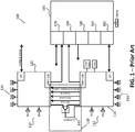
- the current solution for multi-chip cascading is based on wired connections amongst multiple chips located on a single printed circuit board (PCB) 100, as illustrated in FIG. 1 .
- a known radar unit cascades two radar TRx chips.
- One of the radar TRx chips is defined as the master unit 110, which contains a first set of transmitter circuits coupled to transmit antennas 112 and a first set of receiver circuits coupled to receive antennas 114.
- the master unit 110 is arranged to distribute the Local oscillator (LO) signal 140 off-chip through transmission lines on the PCB 100 to other radar chips (in this case the one other TRx chip functioning as a slave unit 120).
- LO Local oscillator
- the slave unit 120 contains a second set of transmitter circuits coupled to transmit antennas 122 and a second set of receiver circuits coupled to receive antennas 124.
- the distribution of the LO signal 140 from the master unit 110 ensures that the slave unit 120 is also able to use the LO signal 140, and thereby ensure that the transmitting signal frequency and the clock frequency of the down mixer of different radar TRx are the same.
- Other control signals may be synchronized with a lower speed clock, for example the ADC clock, which may be used across multiple ICs.
- the master unit 110 is coupled to a signal processing circuit, in the form of a microprocessor IC 160, which includes various interfaces, such as a serial-parallel interface 162, a general purpose input-output port 170, two MIPI-alliance camera serial interfaces (MIPI CSIs) 168, as well as 8 sigma-delta modulators 164 in this illustration and a Pulse width modulation (PWM) circuit 166 for generating calibration signals.
- a signal processing circuit in the form of a microprocessor IC 160, which includes various interfaces, such as a serial-parallel interface 162, a general purpose input-output port 170, two MIPI-alliance camera serial interfaces (MIPI CSIs) 168, as well as 8 sigma-delta modulators 164 in this illustration and a Pulse width modulation (PWM) circuit 166 for generating calibration signals.
- a signal processing circuit in the form of a microprocessor IC 160, which includes various interfaces, such as
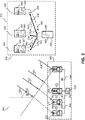
- a block diagram of a radar unit 200 illustrates a further known example of the cascading of multiple chips/ICs with wired interconnections. These chips/ICs are typically the same, in that they each employ the same antennas coupled to one or multiple transceiver circuits, a phase locked loop (PLL) frequency generation circuit, a MCU, etc. Alternatively, the chips/ICs may operate independently as a small radar system.
- an antenna radiation pattern 210 is formed from a plurality of radar transceiver chips and antennas 250 located on a radar unit printed circuit board 220.
- the master radar transceiver unit 230 is only used for generating a common LO signal and multiple control signals for synchronization purposes (as shown in FIG.1 ).
- the master radar transceiver unit 230 requires transmission lines 240 exhibiting equal or known delay, by design.
- FIG. 2 also illustrates two different antenna radiation patterns of a 4-transceivers array 260 and a 16-transceiver array 270 in a rectangular plot, which shows the advantages of cascading a large number of TRx units.
- the LO signal distribution via wired connections from the master unit to all slave units, needs to have equal length to achieve phase coherence when all the TRx channels are used as one antenna array.
- achieving equal delay (or known delays) when distributing LO signals between multiple chips at such high mmWave frequencies is challenging.
- the LO signal is typically in the tens of GHz (e.g. 36GHz (1/2 of the automotive Radar output signal frequency)).
- multiple layers of RF substrate are needed in order to enable mm-wave signal distribution with low loss and well-controlled characteristic impedance, and in order to avoid LO distribution crossing the area of TRx antenna arrays. This invariably leads to higher PCB manufacturing costs and increased complexity.
- the signals needed to be synchronized in order to enable radar chip cascading include: the LO signal, Tx control and frequency chirp control signals, and data capture clock signals (for analog to digital conversion (ADC) start during the signal conversion).
- ADC analog to digital conversion
- Such signals control the transceiver operation of each radar chip, working at the same frequency ramp so that they can capture the received signals at the same moment.
- LO frequency and phase synchronization are critical factors in a distributed phased array design.
- a common phase reference is vital in order to steer the beam and control the radiation pattern for the phased array system.
- US2017/0346575 describes a system for calibrating an antenna array.
- the present invention provides a radar unit, integrated circuit and methods for cascading integrated circuits, as described in the accompanying claims. Specific embodiments of the invention are set forth in the dependent claims. These and other aspects of the invention will be apparent from and elucidated with reference to the embodiments described hereinafter.
- a new architecture is proposed that facilitates a wireless calibration of the multiple chips employed in a radar unit or radar system that employs a phased array.
- a wireless (self) inter-chip localization determination circuit determines a locality value (or values) (or equivalent, such as distance, delays, etc.) between the multiple chips (referred to as 'self-inter-chip localization').
- the wireless (self) inter-chip localization determination circuit obtains delay information, which is calculated based on a self-identification of a distance between antennas of multiple chips. In some examples, this determination is made following a wireless calibration of the different path lengths between multiple chips. In this manner, autonomous forming of a larger phased array system using multiple chips/modules may be achieved. This may result in an enabling of a rapid scaling of a transceiver unit number in a phased array radar system by eliminating a need of wired connections for synchronization.
- Examples of the invention employ wireless synchronization in order to minimize any delay mismatch in either the LO/frequency generation circuitry and/or analog-to-digital converter (ADC) sampling instants (which would ordinarily have led to angle estimation errors) as well as transmit control, frequency chirp start control signals.
- Examples of the invention employ wireless synchronization in an FMCW radar unit, particularly to align the frequency chirp start and end frequencies. The measured distances between antennas of different chips are used to adapt the phase settings of phase shifters in order to steer the antenna beam with increased accuracy.
- examples of the invention allow multiple radar transceiver chips to be located on different PCBs or modules in order to reduce installation complexity in a constructing of an adaptive phased array radar system on a non-planar vehicle surface.
- some examples of the invention propose a method to cascade multiple transceiver chips, for example multiple radar transceiver chips, in order to extend a capability of what can be achieved by a single TRx chip.
- Each chip may have multiple transceiver circuits associated with their corresponding antennas, where the antennas may be located on-chip or located elsewhere on the PCB.
- examples of the invention propose a further fine-tuning technique that combines a wireless synchronization technique with an inter phased array unit ranging technique that includes transmitting a signal to an object and waiting for an echo or acknowledgement signal that is sent back by the object(s). The differences between the transmitting and receiving of signals may be processed in order to acquire the distance information in a known manner. Such information is then used to calibrate a delay to be applied to different units across the multiple chips in a wireless distribution of clock signals, in order to control and accurately synchronise transmission and reception of signals (e.g. their frequency and phase).
- a first example block diagram 300 of a phased array system of a communication unit such as a radar unit 305 includes cascading chips supporting a larger number of TRx chips, enabled as a result of wireless synchronization and distance measurements.
- the radar unit 305 employs multiple chips that use self-inter-chip localisation to synchronise their transmitted signals and calibrate the output phase of each chip, in order to achieve beam steering.
- the radar unit 305 includes a plurality of cascading chips 320, 322, 324, 326 located on respective PCBs and configured to form a phased array system.
- the proposed phased array system is constructed such that a wireless calibration of the cascading chips 320, 322, 324, 326 employed in the radar unit 305 is able to determine a distance between respective antennas between the cascading chips 320, 322, 324, 326, e.g.
- the first cascading chip 320 transmits a wireless inter-chip signal 360 to the second cascading chip 322, and the second cascading chip 322 transmits a wireless inter-chip signal 362 to the third cascading chip 324 and so on such that processing of the respective wireless inter-chip signals may be used to determine/measure a distance between chips (e.g. first distance (d1) 350, second distance (d2) 352 etc ).
- the respective measurements and calculation of distance can be performed on each chip or at a common central control unit 410 that receives the signal transmission and reception information.
- the proposed phased array system is able to identify a signal delay to apply to transmitted or received signals, etc., between the multiple cascading chips 320, 322, 324, 326.
- This wireless calibration is referred to herein as 'self-inter-chip localisation'.
- the use of this wireless calibration and wireless chip synchronization technique may eliminate a known use of wired connections for synchronizing radar TRx chips (e.g. using cables or PCB traces).
- each of the cascading chips 320, 322, 324, 326 is connected to a common central control unit 410 for control and signal processing purposes.
- a common central control unit 410 for control and signal processing purposes.
- the common central control unit 410 may be part of one of the radar units or one of the associated PCB.
- the common central control unit 410 may be a processor integrated circuit (IC) that is configured to act as a master unit processor, arranged to measure and record the distance from all the other ICs or antenna units to itself using a wireless ranging technique. This determination is then used by the common central control unit 410 for the purpose of calibration and performance enhancement of the phased array system, for example to improve angle estimation accuracy and detection range.
- IC processor integrated circuit
- each radar unit may be configured to measure a distance between the antenna on a respective chip and the next antenna, and thereafter feed this information to a central processing unit to form a map of, say, a radar unit installed in a vehicle.
- the d is a priori parameter as the antenna of radar TRX units that are placed with predefined spacing. Any deviation of the real/actual distance value as compared with the predefined spacing will affect the accuracy of the calculation of the angle of arrival.
- common central control unit 410 may be configured to support beam forming across an N-unit phased array radar system following an accurate determination of the correct delay and phase compensation to be applied, which may be based on a distance measurement between the respective antennas or antenna array units of the N-unit phased array radar system.
- the real/actual distance between the antennas in the proposed N-unit phased array radar system may be obtained using a wireless ranging technique with additional built-in hardware, for example as described with reference to the self-inter-chip distance measurement transceiver(s) 570 of FIG. 5 .
- the accurate measurement of the distance value d may then be used to calibrate/set the phase delay/shift of different TRx units for accurate object location detection and/or steering the direction of the antenna beam (e.g. control its radiation pattern).
- beam steering can be implemented by adding the received signals 422, 424, 426, 428 from an N-unit phased array radar system after correct delay and phase compensation, as calculated by the common central control unit 410.
- the use of a phased array increases the sensitivity by 'N' times, as compared to that of a single unit.
- beam steering can also be implemented by shifting the phase of the transmitting signals of an N-unit phased array radar system. For multiple mid-range radar units, the inputs to an N-unit phased array radar system can be combined in order to increase the radar transmit power, and thereby allow longer range applications.
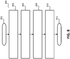
- a second example block diagram 370 of a phased array radar system of a radar unit 372 includes a master radar chip 380 and multiple radar slave chips 382, 384, 386.
- Each radar slave chip 382, 384, 386 contains at least a radar transceiver, a broadcast receiver and a self-inter-chip localisation transceiver 389.
- Each radar master chip 380 contains at least a broadcast transmitter 383 and a self-inter-chip localisation transceiver 389.
- the master radar chip 380 generates the signal modulation and broadcasts a transmit signal via, say, an intermediate-frequency signal to the slave radar chips 382, 384, 386 through the respective broadcast links 374, 376, 378.
- the broadcast links 374, 376, 378 operate at a fraction of the transmit frequency power in order to avoid interfering with the normal radar operation.
- the radar slave chips 382, 384, 386 may contain frequency multipliers in order to up-convert the broadcast transmit signal to a higher frequency, before the output signal is transmitted by the slave transmit antenna 397, 398, 399,
- the first slave chip 382 transmits a wireless inter-chip signal 390 to the second slave chip 384 and the second cascading chip 384 transmits a wireless inter-chip signal 391 to a third ('N') cascading chip 386 and so on, such that processing of the wireless inter-chip signals may be used to determine/measure a distance between slave chips (e.g. in a similar manner to the distances determined in the first example block diagram 300).
- an alternative example system design employs one central unit (i.e. master unit 380) configured to generate the LO signal and distribute the LO signal and various control signals, such as wireless inter-chip signals 392, 393, 394, to slave units 382, 384, 386.
- master unit 380 configured to generate the LO signal and distribute the LO signal and various control signals, such as wireless inter-chip signals 392, 393, 394, to slave units 382, 384, 386.
- the slave units 382, 384, 386 may have less complex hardware and act as repeaters, but with correct power and phase control.
- the respective measurements and calculation of distance may be performed on each slave chip 382, 384, 386 and relayed to the master unit 380 or the distances calculated at the master unit 380 in response to receiving the signal transmission and reception times of the wireless inter-chip signals from the slave chips 382, 384, 386.
- the proposed phased array system is able to identify a signal delay to apply to transmitted or received signals, etc., between the multiple slave chips 382, 384, 386, as well as from the master chip 380 and each respective slave chip 382, 384, 386 in a form of 'self-inter-chip localisation'.
- the use of this wireless calibration may eliminate a known use of wired connections for synchronizing radar TRx chips (e.g. using cables or PCB traces).
- the proposed phased array system with a wireless calibration of a distance between the cascading chips allows the phased array system to include a larger number of transceiver (TRx) chips than can currently be supported per radar unit with a similar profile (e.g. size).
- TRx transceiver
- the self-distance measurement between radar chips may be based on a determined round trip time of flight measurement, which provides distance information between respective array units.
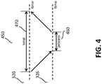
- the distance information between respective array units may be used in angle of arrival estimation calculations (as illustrated in FIG. 4 ).
- the distance information between respective array units may be used in beam steering calculations, for example to manipulate a beam pattern.
- the beam steering calculations may be employed in a steering phased array antenna main beam, in order to locate a direction of incoming signal and gain spatial information of the interferers.
- the radar unit may perform electronical steering of the antenna beam to cover a wide range of directions.
- An MCU of the radar unit may re-configure, using for example control signal from MCU 410 or master unit 380 in FIG. 3 , a phased array detection path in order to scan different frequencies and/or adjust phased array circuits.
- the phased array circuits may be composed of multiple, adjustable, parallel and/or selectable delays (not shown), in order to create stronger transmitter and/or receiver active beams, and in some examples create beam 'nulls' for example in a direction of an identified interferer.
- the MCU 410 or master unit 380 of the radar unit may adjust the delay/phase difference amongst different paths, and thus the direction of the transmitting signal beam can be adjusted.
- the MCU 410 or master unit 380 of the radar unit may adjust the delay/phase difference amongst different paths, and thus the direction of the receiving signal beam can be adjusted by a phased array receiver.
- the strength of the beam indicates the gain of the antenna.
- phased array system of example embodiments of the invention is able to benefit from improved accuracy as a result of wireless synchronization and control of transmitted and received signals and distance measurements between antennas in a multiple TRx chip configuration.
- a wireless synchronization of control signals and inter-chip ranging (e.g. distance determination) technique may share the same hardware but use a different signal frequency from the normal radar signal, thereby allowing the technique to operate in the background of normal radar communications and not interfere therewith.
- the use of a wireless synchronization of control signals may avoid a need to include complicated LO distribution circuitry and traces on the PCB and allow a reduction in the number of RF substrate layers required, as only a single RF substrate is needed for TRx antenna array. This approach allows also cascading of radar TRx chips on different PCBs or modules without a need of cable interconnection, which also leads to a cost reduction.
- the use of a wireless synchronization of control signals together with an inter-chip ranging (e.g. distance determination) technique may enable a rapid scaling of the number of radar TRx units in a multiple-in multiple-out (MIMO) or phased array radar system and avoid the burden of re-designing a PCB every time the number of TRx units is to be increased.
- this combination of features may also enable a construction of an adaptive phased array radar system, for example on a non-planar vehicle surface.
- the adaptive phased array radar system may include uniform linear arrays, uniform rectangular arrays, uniform circular arrays, or even conformal arrays.
- FIG. 4 illustrates one example of a mechanism to calculate a distance measurement between antennas of radar units 320 and 326, otherwise referred to herein as wireless localization using a roundtrip time of flight (ToF) measurement method 450.
- ToF roundtrip time of flight
- the T total time 470 is a measured parameter and a T process 460 is a known parameter.
- the radar unit 500 is composed of arrays of transmitters and receivers configured to operate in a frequency modulated continuous wave (FMCW) mode of operation, whereas in other examples (not shown) the radar unit may be composed of a single or a wideband transceiver and/or be configured to operate with other radar modes of operation.
- Other radar modes of operation may include, for example, pulse mode continuous wave (PMCW), frequency shift keyed (FSK), ultra-wideband (UWB) impulse radar, Pulse Doppler radar.
- PMCW pulse mode continuous wave
- FSK frequency shift keyed
- UWB ultra-wideband
- the use of transceiver arrays enables the number of transmitter and receiver channels that can be supported by the radar unit 500 architecture to be scalable.
- a microprocessor unit (which may be located in a dedicated processor integrated circuit (IC)) 552 is configured to perform digital control and signal processing that provides a first transmit radar signal 554 to a local oscillator and frequency generation circuit that includes a waveform generator 542 in, say, an analog/mixed signal baseband circuit.
- the waveform generator 542 provides a signal 538 that is to be modulated by a voltage controlled oscillator circuit 526.
- the modulated signal is then optionally passed to a buffer 524 or frequency multiplier in the main radar transmit path (if the voltage controlled oscillator (VCO) generated signal is not at the operating frequency of the FMCW radar unit 500).
- VCO voltage controlled oscillator
- the high-frequency output 532 of the buffer 524 or frequency multiplier is passed to a power amplifier 522 via a phase shifter circuit 536 (such as the phase shifter circuit illustrated and described with reference to FIG. 6 ), where it is amplified and routed to the one or more transmitter antenna(e) 510.
- a phase shifter circuit 536 such as the phase shifter circuit illustrated and described with reference to FIG. 6
- the localization processing circuit 580 is configured to adjust at least one phase shifter, e.g. one or more of phase shifters 536 in a transmitter sense, or one or more phase shifters 592 in a digital domain in a receiver sense, e.g. to perform digital beamforming, in response to the wirelessly determined distance relationship.
- a phase control unit 602, operably coupled to the localization processing circuit 580 is configured to adjust at least one phase shifter 616 in response to the wirelessly determined distance relationship
- a first received radar signal may be received at the one or more receiver antenna(s) 512 and passed to a low noise amplifier (LNA) 528 where it is amplified.
- the amplified received radar signal is passed to a down-mixer 530, where it is mixed with the high-frequency signal 532 output from the VCO 526.
- the down-converted received radar signal 534 from down-mixer 530 is input to a programmable baseband circuit 544.
- the programmable base-band circuit 544 implements one or more programmable bandpass filter(s) and one or more gain amplifiers, as well as a highly linear ADC that processes a relative narrow band signal, for example in a range between a few kHz up to tenths of MHz.
- the programmable base-band circuit 544 outputs a narrowband, high linearity digitized signal 556 to the digital control and signal processing unit 552 for processing and the received processed radar signal 558 is output.
- the control signals 594 which are much lower frequency signals (tenths of MHz or lower) compared to the LO signal (of tenths of GHz) may be used to modulate the amplitude of the transmitted LO signal.
- control signals 594 such as measurement and control, data and clock signals, calibration, configuration and status control signals, etc.
- distributed by signal processing unit 552 may be synchronized and/or distributed wirelessly as information modulated onto the LO signal, as these control signals 594 are at relatively low frequency.
- the radar unit 500 has been configured to include one or more additional self inter-chip distance measurement transceiver(s) 570 that facilitate self inter-chip distance measurement.
- the one or more additional transceiver(s) 570 includes at least one power amplifier 582 configured to amplify a signal for use in a self inter-chip distance measurement that is routed to one or more additional transmitter antenna(s) 584.
- the one or more additional transceiver(s) 570 also includes one or more additional receiver antenna(s) 574, LNA 576, down-mixer 578 and localization processing circuit 580 that is detection receiver(s) configured to perform a synchronization of received signals and encoding and decoding operations for wireless inter-chip/antenna distance measurements.
- the localization processing circuit 580 may also be configured to generate a number of TRx control signals 594.
- the output signal from LO 526 is also routed to a clock divider and/or frequency multiplier circuit 527 for down-mixing the wireless synchronization received signals and for the divided down clock signals to be used by the self inter-chip distance measurement transceiver(s) 570 in synchronizing the LO signals among different radar units, as well as encoding and decoding operations.
- self inter-chip distance measurement transceiver(s) 570 may vary slightly in design.
- FIG. 5 illustrates a single additional self inter-chip distance measurement transceiver(s) 570
- multiple additional self inter-chip distance measurement transceivers 570 may be used, in a similar manner to the multiple main radar transmitter and receiver paths.
- the illustrated self inter-chip distance measurement and LO/control signal 594 distribution are based on continuous wave techniques such as FMCW, it is envisaged that the concepts herein described are equally applicable to a pseudo noise (PN)-code modulated CW principle or pulsed architectures, such as ultra wideband (UWB) impulse radio.
- PN pseudo noise
- UWB ultra wideband
- the one or more additional self inter-chip distance measurement transceiver(s) 570 in each radar IC is configured to transmit a detection signal to other ICs in order to determine a distance measurement between the antennas of respective ICs based on, say, a ToF technique as described with reference to FIG. 4 .
- the detection receiver(s) may be located remotely from the dedicated processor IC 552, however in other examples it is envisaged that the detection receiver(s) may be incorporated into dedicated processor IC 552.
- the dedicated processor IC 552 (or processor IC 580) may be configured to extract or determine the one or more delays, and/or calculate the respective distance information between antennas under measurement.
- clock divider and/or frequency multiplier circuit 527 may incorporate any high frequency clock distribution topology, such as that described in X. Guo, D.-J. Yang, R. Li, and K. K. O, "A Receiver with Start-up Initialization and Programmable Delays for Wireless Clock Distribution," and published in 2006 IEEE International Solid State Circuits Conference - Digest of Technical Papers, 2006, pp. 1530-1539 .
- Examples of the invention can readily use a variation of the 18GHz clock receiver described in this paper with a technique to avoid the problem of start up with random phases.
- a monotone sine wave may be used for clock distribution to reduce the complexity.
- phase shifter 536 implementation in a transmitter for beamforming is illustrated, according to example embodiments of the invention.
- an input local oscillator (LO) signal 606 is fed to a quadrature (I/Q) signal generator 610, which outputs quadrature signals 620, 622, 624, 626 (i.e. quadrature shifted components of the input signal 606) of 90 deg. separation.
- the quadrature signals 620, 622, 624, 626 are input to respective variable analog phase shifters 616, controlled by phase control unit 602 via control paths 608.
- phase control unit 602 is able to respectively adjust the phase of any of the quadrature signals 620, 622, 624, 626, to produce output (potentially phase shifted) quadrature signals 630, 632, 634, 636.
- the output (potentially phase shifted) quadrature signals 630, 632, 634, 636 are combined in summing junction 618 that produces an output signal 638. In this manner, substantially 90 degrees phase shifted LO signals are summed with respective phase-shifting effectively applied.
- An inter array distance measurement circuit 604 is connected to the phase control unit 602 to implement the calculated required phase shift ( ⁇ ) for configuring the variable analog phase shifters 616 in the phased array system.
- the inter array distance measurement circuit 604 may assist a calibrating of a set of predefined values, in order to enhance system performance in terms of angular accuracy, for example, especially for a non-uniform phased array.
- the distance measurement information obtained by the inter array distance measurement circuit 604 is used to control the phase shifters (e.g. the amount of phase difference between the signals passing there through) of the transmitters in a multi-chip phased array system.
- the aforementioned examples may be suited for lower power applications as the above examples eliminate the need for an additional power hungry LO buffer in order to drive long transmission lines off-chip on a PCB.
- the radar system may benefit from increased flexibility with the opportunity to introduce a larger antenna array around the vehicle, e.g. with a 360 degree view.
- the use of a wireless communication link removes a need for installing expensive and potentially heavy cables.
- examples of the invention readily enable an extension of the radar system to include multiple ICs in the same or separated PCBs or packages.
- the wireless synchronization may also be used to transmit data and/or control signals, where the control signals are required to setup the co-operation of the units in the phased array system, so that many more radar ICs can be calibrated and used.
- the radar units that include a built-in inter-chip localization feature may be employed in radar units in vehicles, for example in the radar sensors 710 in the vehicle 700 of FIG. 7 .
- Examples of the invention may be additionally employed to support beam steering control in a phased array radar system across multiple sensors, in some examples having multiple chips.
- Examples of the invention propose a method for cascading a plurality of mmW TRx integrated circuits in a radar unit configured to support a normal radar mode of operation that comprises transmitting a radar signal waveform and receiving an echo signal thereof, each comprising at least one phase shift circuit and each coupled to respective antennas.
- the method comprises: processing transmit and receive signals of the plurality of cascaded mmW TRx ICs, wirelessly transmitting a signal from a first TRx circuit of an auxiliary mmW TRx ICs to a second TRx IC of the auxiliary mmW via a respective antenna, determining a distance relationship between at least one antenna coupled to the first TRx IC and at least one antenna coupled to the second TRx IC by a localization processing circuit operably coupled to at least one of the first TRx IC and second TRx IC; and adjusting at least one phase shifter by a phase control unit, operably coupled to the localization processing circuit, in response to the wirelessly determined distance relationship.
- a waveform generator of a master unit controls its VCO to output a LO signal with a fixed frequency that is proportional to a chirp start frequency, f start_master , at 804.
- slave units are initiated to receive the signal from the master unit, and accordingly adjust their LO frequency to be the same as that in the master unit.
- the slave units record the control bits.
- this signal may be processed by the 'clock divider or multiplier' circuit 527 shown in FIG. 5 and sent out by the transmitter to other chips/antenna of the radar unit.
- the slave units may also be configured with the same setting (the digital control bits in order to set the LO signal frequency) to output a LO signal with frequency f state_slaveN .
- the LO frequency of the slave unit(s) will then be adjusted by the digital control bits until they are the same as that in the master unit, in 810.
- the digital control bits of the 'LO and frequency chip generation circuits', for generating the chirp start frequency will be updated. In this manner, the same procedure for the synchronization of the f end_slaveN and f end_master is employed, after which, all the slave units will have the same frequency chirp start and end frequencies.
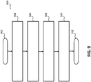
- FIG. 9 a second example flowchart 900 according to the first example block diagram of a phased array radar system of FIG. 3 , is illustrated according to example embodiments of the invention.
- the second example flowchart 900 starts at 902 and moves to 904 where the N-unit phased array radar system is initialized, and a central control unit (e.g. microcontroller unit (MCU) 410 of FIG. 3 ) communicates to respective radar transceiver units to start a synchronization phase.
- MCU microcontroller unit
- each chip of the radar unit automatically synchronizes their LO and analog-to-digital converter (ADC) clock and other control signals, and measures the distance to one or more of its neighbouring chips/antennas, for example in accordance with one of the techniques described in FIG. 4 , or using in other examples, say, laser sensors to achieve a higher accuracy distance measurement.
- ADC analog-to-digital converter
- laser technology is also considered as a wireless technology (where light has a much higher frequency with a wavelength of a few hundred nm). The benefit of using a laser for short distance measurements is that the measurement accuracy is much higher.
- laser technology using the architecture in FIG. 3 will be particularly useful in the future for high-end applications.
- the multi chips phased array system is configured or calibrated to have the desired phase delay/phase shift settings.
- the synchronization process ends and the normal radar detection phase starts, with all radar tranceiver units working together as one phased array system. The flowchart then ends at 912.
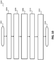
- a third example flowchart 1000 according to the second example block diagram of a phased array radar system of FIG. 3 , is illustrated according to example embodiments of the invention.
- the third example flowchart 1000 starts at 1002 and moves to 1004, where the master radar unit measures the distance to the slave radar units.
- each slave radar unit measures the distance to its nearby slave radar unit(s) using an auxiliary wireless link, as described earlier in the example of FIG. 5 .
- the multi chips phased array system is configured or calibrated to have the desired phase delay/phase shift settings.
- the master radar unit transmits the radar signal to the slave radar units at an intermediate frequency.
- the slave radar units upconvert the signal coming from the master radar unit and transmit the upconverted signal with the desired phase shift.
- the flowchart then ends at 1014.
- examples of the invention describe a radar system that includes an enhanced target detection and direction finding mechanism, with a deterministic initial phase shift value being used.
- improved flexibility in, say, a beam steering application can be achieved by supporting many more ICs than in current systems, through use of wireless distribution of control signals and associated calibration of distances between the ICs.
- the architecture herein described may be used, say as a FMCW where more output power is concentrated in one frequency, so it has a better range performance.
- the architecture herein described may be used, say, as a PMCW radar when the prevailing operational condition(s) is/are less susceptible to interference, but where there is a lower peak power and a demand for more computational power.
- the architecture herein described may be used, say, as a UWB impulse radar, when a good range resolution is desired and where it may be easy to adapt the range resolution by adjusting a radar pulse width.
- the architecture herein described may be used, say, as a UWB impulse radar when it also has a low power consumption and may be needed to provide a wide coverage in azimuth angle but only provide range information, such as for a parking or stop and go sensor.
- connections as discussed herein may be any type of connection suitable to transfer signals from or to the respective nodes, units or integrated circuit devices. Accordingly, unless implied or stated otherwise, the connections may for example be direct connections or indirect connections. Also, plurality of connections may be replaced with a single connection that transfers multiple signals serially or in a time multiplexed manner. Likewise, single connections carrying multiple signals may be separated out into various different connections carrying subsets of these signals. Therefore, many options exist for transferring signals.
- any two components herein combined to achieve a particular functionality can be seen as 'associated with' each other such that the desired functionality is achieved, irrespective of architectures or intermediary components.
- any two components so associated can also be viewed as being 'operably connected,' or 'operably coupled,' to each other to achieve the desired functionality.
- the illustrated examples may be implemented as circuitry located on a single integrated circuit or within a same device.
- the circuit and/or component examples may be implemented as any number of separate integrated circuits or separate devices interconnected with each other in a suitable manner.
- the specifications and drawings are, accordingly, to be regarded in an illustrative rather than in a restrictive sense.
- any reference signs placed between parentheses shall not be construed as limiting the claim.
- the word 'comprising' does not exclude the presence of other elements or steps then those listed in a claim.
- the terms 'a' or 'an,' as used herein, are defined as one, or more than one.
Claims (9)
- Radareinheit (500), die Folgendes umfasst:ein Radarsystem mit phasengesteuerter Vielfachantenne, umfassend mehrere kaskadierte integrierte Millimeterwellen-Sendeempfänger-Schaltungen, mmW TRx ICs, ausgelegt zum Unterstützen eines normalen Radarbetriebsmodus, der Senden einer Radarsignalwellenform und Empfangen eines Echosignals davon umfasst, wobei jede mmW TRx IC zumindest eine Phasenverschiebungsschaltung (616) umfasst und jede mit entsprechenden Antennen gekoppelt ist; undeine Signalprozessorschaltung (552), wirkgekoppelt mit den mehreren kaskadierten mmW TRx ICs und ausgelegt zum Verarbeiten von Sende- und Empfangssignalen der mehreren kaskadierten mmW TRx ICs; wobei die Radareinheit (500) gekennzeichnet ist durch:eine unterstützende mmW TRx IC (570), wirkgekoppelt mit der Signalprozessorschaltung (552) und umfassend eine erste TRx IC (320) und eine zweite TRx IC (322),wobei die erste TRx IC (320) der unterstützenden mmW TRx IC (570) ausgelegt ist zum kabellosen Senden (360) eines Signals an die zweite TRx IC (322) der unterstützenden mmW TRx IC (570) über eine entsprechende Antenne;eine Lokalisierungsverarbeitungsschaltung (580), wirkgekoppelt mit zumindest einer aus der ersten TRx IC (320) und der zweiten TRx IC (322) und ausgelegt zum Bestimmen einer Abstandsbeziehung (350) zwischen zumindest einer Antenne, die mit der ersten TRx IC (320) gekoppelt ist, und zumindest einer Antenne, die mit der zweiten TRx IC (322) gekoppelt ist; undeine Phasensteuerungseinheit (602), wirkgekoppelt mit der Lokalisierungsverarbeitungsschaltung (580) und ausgelegt zum Einstellen der zumindest einen Phasenverschiebungsschaltung (616) in Reaktion auf die kabellos bestimmte Abstandsbeziehung.
- Radareinheit (500) nach Anspruch 1, wobei die Abstandsbeziehung eines oder mehrere aus Folgendem umfasst: einen geografischen Abstand zwischen einer Anzahl der mehreren mmW-TRx-Antennen, eine Sendeverzögerung zwischen zumindest einer Anzahl der mehreren mmW-TRx-Schaltungen.
- Radareinheit (500) nach Anspruch 1 oder Anspruch 2, wobei die mehreren kaskadierten mmW TRx ICs zumindest die erste TRx IC (320) und die zweite TRx IC (322) umfassen.
- Radareinheit (500) nach Anspruch 3, wobei die unterstützende mmW-TRx-Schaltung (570) eine Haupt-Sendeempfängerschaltung (380) umfasst, die ausgelegt ist zum Erzeugen einer Signalmodulation und zum Rundsenden eines Sendesignals über ein Zwischenfrequenzsignal an die mehreren kaskadierten mmW-TRx-Schaltungen zu einem Bruchteil der Sendefrequenzleistung, um Interferenzen mit dem normalen Betriebsmodus zu vermeiden.
- Radareinheit (500) nach einem der vorhergehenden Ansprüche, wobei die Radareinheit eine frequenzmodulierte Dauerstrichradareinheit, FMCW, (500) ist und die Phasenverschiebungssteuereinheit (602) ausgelegt ist zum Ausrichten der Start- und Endfrequenzen des Frequenz-Chirps der FMCW-Radareinheit (500) beim Einstellen des zumindest einen Phasenschiebers (616).
- Radareinheit (500) nach einem der vorhergehenden Ansprüche, wobei die Signalprozessorschaltung (552) mit einer Frequenzerzeugungsschaltung wirkgekoppelt ist, die ausgelegt ist zum Erzeugen eines lokalen Oszillatorsignals (LO) zur Verwendung durch die kaskadierten mmW TRx ICs in der Radareinheit, und wobei die Signalprozessorschaltung (552) ausgelegt ist zum kabellosen Verteilen von Steuersignalen (594) innerhalb der Radareinheit durch Modulieren einer Amplitude des LO-Signals.
- Radareinheit (500) nach einem der vorhergehenden Ansprüche, wobei die entsprechenden Antennen, die mit den mehreren kaskadierten mmW TRx ICs gekoppelt sind, dazu ausgelegt sind, als eine phasengesteuerte Vielfachantenne zu arbeiten.
- Radareinheit (500) nach Anspruch 7, wobei die Lokalisierungsverarbeitungsschaltung (580) dazu ausgelegt ist, Berechnungen zur Abschätzung des Einstrahlwinkels zwischen entsprechenden Vielfachantennenelementen der phasengesteuerten Vielfachantenne durchzuführen, und wobei die Phasensteuereinheit (602) ausgelegt ist zum Umsetzen von Phasenverschiebungen zum Unterstützen der Strahllenkung der phasengesteuerten Vielfachantenne.
- Verfahren zum Kaskadieren von mehreren integrierten Millimeterwellen-Sendeempfänger-Schaltungen, mmW TRx ICs, in einer Radareinheit (500), umfassend ein Radarsystem mit phasengesteuerter Vielfachantenne, ausgelegt zum Unterstützen eines normalen Radarbetriebsmodus, der Senden einer Radarsignalwellenform und Empfangen eines Echosignals davon umfasst, wobei jede mmW TRx IC zumindest eine Phasenverschiebungsschaltung (616) umfasst und jede mmW TRx IC mit entsprechenden Antennen gekoppelt ist, wobei das Verfahren Folgendes umfasst:Verarbeiten von Sende- und Empfangssignalen der mehreren kaskadierten mmW TRx ICs;wobei das Verfahren gekennzeichnet ist durch:kabelloses Senden (360) eines Signals von einer ersten TRx IC (320) einer unterstützenden mmW TRx IC (570) der Radareinheit (500) an eine zweite TRx IC (322) der unterstützenden mmW TRx IC (570) über eine entsprechende Antenne;Bestimmen einer Abstandsbeziehung zwischen zumindest einer Antenne, gekoppelt mit der ersten TRx IC (320), undzumindest einer Antenne, gekoppelt mit der zweiten TRx IC (322), durch eine Lokalisierungsverarbeitungsschaltung (580), wirkgekoppelt mit zumindest einer aus der ersten TRx IC (320) und der zweiten TRx IC (322); undEinstellen der zumindest einen Phasenverschiebungsschaltung (616) durch eine Phasensteuereinheit (602), wirkgekoppelt mit der Lokalisierungsverarbeitungsschaltung (580), in Reaktion auf die kabellos bestimmte Abstandsbeziehung.
Priority Applications (2)
| Application Number | Priority Date | Filing Date | Title |
|---|---|---|---|
| EP17207040.1A EP3499264B1 (de) | 2017-12-13 | 2017-12-13 | Radareinheit und verfahren zur kaskadierung von integrierten schaltungen in einer radareinheit |
| US16/174,997 US10983193B2 (en) | 2017-12-13 | 2018-10-30 | Communication unit, integrated circuits and methods for cascading integrated circuits |
Applications Claiming Priority (1)
| Application Number | Priority Date | Filing Date | Title |
|---|---|---|---|
| EP17207040.1A EP3499264B1 (de) | 2017-12-13 | 2017-12-13 | Radareinheit und verfahren zur kaskadierung von integrierten schaltungen in einer radareinheit |
Publications (2)
| Publication Number | Publication Date |
|---|---|
| EP3499264A1 EP3499264A1 (de) | 2019-06-19 |
| EP3499264B1 true EP3499264B1 (de) | 2020-07-01 |
Family
ID=60673377
Family Applications (1)
| Application Number | Title | Priority Date | Filing Date |
|---|---|---|---|
| EP17207040.1A Active EP3499264B1 (de) | 2017-12-13 | 2017-12-13 | Radareinheit und verfahren zur kaskadierung von integrierten schaltungen in einer radareinheit |
Country Status (2)
| Country | Link |
|---|---|
| US (1) | US10983193B2 (de) |
| EP (1) | EP3499264B1 (de) |
Cited By (1)
| Publication number | Priority date | Publication date | Assignee | Title |
|---|---|---|---|---|
| US20200292666A1 (en) * | 2019-03-12 | 2020-09-17 | Uhnder, Inc. | Multi-chip synchronization for digital radars |
Families Citing this family (26)
| Publication number | Priority date | Publication date | Assignee | Title |
|---|---|---|---|---|
| US9846228B2 (en) | 2016-04-07 | 2017-12-19 | Uhnder, Inc. | Software defined automotive radar systems |
| US10261179B2 (en) | 2016-04-07 | 2019-04-16 | Uhnder, Inc. | Software defined automotive radar |
| US11105890B2 (en) | 2017-12-14 | 2021-08-31 | Uhnder, Inc. | Frequency modulated signal cancellation in variable power mode for radar applications |
| US11237249B2 (en) * | 2018-01-22 | 2022-02-01 | Mediatek Inc. | Apparatus and method for applying frequency calibration to local oscillator signal derived from reference clock output of active oscillator that has no electromechanical resonator |
| US10804616B2 (en) * | 2018-03-27 | 2020-10-13 | Viasat, Inc. | Circuit architecture for distributed multiplexed control and element signals for phased array antenna |
| JP6923478B2 (ja) * | 2018-03-28 | 2021-08-18 | 日立Astemo株式会社 | レーダセンサ |
| US11002844B2 (en) * | 2018-11-08 | 2021-05-11 | Infineon Technologies Ag | Radar system with internal ramp linearity measurement capability |
| US10884100B2 (en) * | 2018-11-29 | 2021-01-05 | Toyota Jidosha Kabushiki Kaisha | Multi-carrier modulation on FMCW radar for integrated automotive radar and communication systems |
| EP3696909B1 (de) * | 2019-02-15 | 2023-12-20 | IMEC vzw | Mehrchip-system für eine antennenanordnung |
| DE102019110525B4 (de) * | 2019-04-23 | 2021-07-29 | Infineon Technologies Ag | Kalibrierung eines radarsystems |
| DE102020107804A1 (de) * | 2019-04-26 | 2020-10-29 | Infineon Technologies Ag | Radarvorrichtung und Verfahren zum Detektieren von Radarzielen |
| DE102019110840A1 (de) * | 2019-04-26 | 2020-10-29 | Infineon Technologies Ag | Rf-vorrichtungen mit konformen antennen und verfahren zu deren herstellung |
| US11637368B2 (en) * | 2019-07-18 | 2023-04-25 | The Boeing Company | Phased array passband calibration |
| DE102019211431A1 (de) * | 2019-07-31 | 2020-07-09 | Audi Ag | Verfahren zum Betrieb von Radarsensoren in einem Kraftfahrzeug und Kraftfahrzeug |
| CN110501703A (zh) * | 2019-08-28 | 2019-11-26 | 南京德睿智芯电子科技有限公司 | 一种小型成像雷达射频收发模块 |
| KR20210082946A (ko) | 2019-12-26 | 2021-07-06 | 삼성전자주식회사 | 레이더 신호 처리 장치 및 방법 |
| CN111352082B (zh) * | 2020-01-07 | 2022-01-07 | 浙江大学 | 基于分层共形曲面的有源相控阵雷达安装位置测量方法 |
| WO2021144710A2 (en) * | 2020-01-13 | 2021-07-22 | Uhnder, Inc. | Method and system for multi-chip operation of radar systems |
| KR20210096433A (ko) * | 2020-01-28 | 2021-08-05 | 엘지전자 주식회사 | 자율 주행 차량 및 그 제어 방법 |
| US20210364596A1 (en) * | 2020-05-20 | 2021-11-25 | Infineon Technologies Ag | Processing radar signals |
| US20210389447A1 (en) * | 2020-06-12 | 2021-12-16 | Metawave Corporation | Method and apparatus for non-line of sight radar |
| EP4244988A1 (de) * | 2021-01-06 | 2023-09-20 | Viasat Inc. | Kalibrierung einer spärlichen antennenanordnung |
| EP4040600A1 (de) * | 2021-02-04 | 2022-08-10 | Urugus S.A. | Softwaredefiniertes kommunikationssystem und vorrichtung |
| CN113055000B (zh) * | 2021-03-23 | 2023-08-11 | 加特兰微电子科技(上海)有限公司 | 传感系统、相关装置及工作时钟信号的获取方法 |
| US11919479B2 (en) * | 2021-05-18 | 2024-03-05 | Ford Global Technologies, Llc | Systems and methods for providing security to a vehicle |
| US20230160998A1 (en) * | 2021-11-24 | 2023-05-25 | Gm Cruise Holdings Llc | Modular radar element wireless synchronization |
Family Cites Families (6)
| Publication number | Priority date | Publication date | Assignee | Title |
|---|---|---|---|---|
| US7409022B2 (en) | 2004-10-01 | 2008-08-05 | Mitsubishi Electric Research Laboratories, Inc. | Synchronizing clocks in wireless personal area networks |
| US8494030B2 (en) | 2008-06-19 | 2013-07-23 | Broadcom Corporation | Method and system for 60 GHz wireless clock distribution |
| ATE530923T1 (de) * | 2009-04-20 | 2011-11-15 | Univ Duisburg Essen | Master-sende-empfangsgerät und slave-sende- empfangsgerät zur bestimmung von bereichsinformation |
| EP2881752B1 (de) | 2013-12-03 | 2017-05-10 | Nxp B.V. | Multichip-Kfz-Radarsystem, Radarchip für ein solches System, und Verfahren zum Betrieb eines solchen Systems |
| US10324179B2 (en) * | 2015-05-01 | 2019-06-18 | Maxlinear, Inc. | Multistatic radar via an array of multifunctional automotive transceivers |
| US9948407B2 (en) * | 2016-05-27 | 2018-04-17 | Huawei Technologies Co., Ltd. | Method and apparatus for beamforming calibration in point to multipoint communication systems |
-
2017
- 2017-12-13 EP EP17207040.1A patent/EP3499264B1/de active Active
-
2018
- 2018-10-30 US US16/174,997 patent/US10983193B2/en active Active
Non-Patent Citations (1)
| Title |
|---|
| None * |
Cited By (2)
| Publication number | Priority date | Publication date | Assignee | Title |
|---|---|---|---|---|
| US20200292666A1 (en) * | 2019-03-12 | 2020-09-17 | Uhnder, Inc. | Multi-chip synchronization for digital radars |
| US11977178B2 (en) * | 2019-03-12 | 2024-05-07 | Uhnder, Inc. | Multi-chip synchronization for digital radars |
Also Published As
| Publication number | Publication date |
|---|---|
| US10983193B2 (en) | 2021-04-20 |
| US20190178983A1 (en) | 2019-06-13 |
| EP3499264A1 (de) | 2019-06-19 |
Similar Documents
| Publication | Publication Date | Title |
|---|---|---|
| EP3499264B1 (de) | Radareinheit und verfahren zur kaskadierung von integrierten schaltungen in einer radareinheit | |
| CN106574967B (zh) | 在雷达中用于使振荡器信号同步的回送技术 | |
| CN108603928B (zh) | 用于降低由雷达系统中的相位噪声引起的干扰的方法和系统 | |
| US10782389B2 (en) | Linear, synthesized radar receiver array between and extending from ICS | |
| US10823819B2 (en) | Radar system including an antenna array for transmitting and receiving electromagnetic radiation | |
| US9998170B2 (en) | Active phased array transmitter, active phased array receiver, and active phased array transceiver | |
| JP6252314B2 (ja) | フェーズドアレイ送信機,送受信機およびレーダー装置 | |
| JP7066015B2 (ja) | アンテナ装置及びレーダ装置 | |
| Dürr et al. | High-resolution 160-GHz imaging MIMO radar using MMICs with on-chip frequency synthesizers | |
| Steinhauer et al. | Millimeter-wave-radar sensor based on a transceiver array for automotive applications | |
| CN109407056A (zh) | 具有hf振荡器监控的雷达前端 | |
| US20050156780A1 (en) | Methods and apparatus for automotive radar sensors | |
| US11567170B2 (en) | Calibration of a radar system using plurality of phase shifted oscillator signals | |
| Feger et al. | A frequency-division MIMO FMCW radar system based on delta–sigma modulated transmitters | |
| US20230109403A1 (en) | Self-calibrating phased-array transceiver | |
| JP2017147496A (ja) | 複数の送信アンテナの位相校正装置 | |
| JP6701124B2 (ja) | レーダ装置 | |
| US11349208B2 (en) | Antenna apparatus with switches for antenna array calibration | |
| CN110741274B (zh) | 用于补偿二次雷达系统中的噪声或系统偏差的方法和装置 | |
| JP6844525B2 (ja) | アンテナ装置 | |
| Lutz et al. | Target simulator concept for chirp modulated 77 GHz automotive radar sensors | |
| CN110609272A (zh) | 在雷达系统中的相位测量 | |
| US11353570B2 (en) | Radar system and method for operating a radar system | |
| WO2023210451A1 (ja) | 測位システムおよびそれを備える車両、並びに測位方法 | |
| US11879968B2 (en) | Simultaneous beamforming and multiple input-multiple output (MIMO) schemes in radar system |
Legal Events
| Date | Code | Title | Description |
|---|---|---|---|
| PUAI | Public reference made under article 153(3) epc to a published international application that has entered the european phase |
Free format text: ORIGINAL CODE: 0009012 |
|
| STAA | Information on the status of an ep patent application or granted ep patent |
Free format text: STATUS: THE APPLICATION HAS BEEN PUBLISHED |
|
| AK | Designated contracting states |
Kind code of ref document: A1 Designated state(s): AL AT BE BG CH CY CZ DE DK EE ES FI FR GB GR HR HU IE IS IT LI LT LU LV MC MK MT NL NO PL PT RO RS SE SI SK SM TR |
|
| AX | Request for extension of the european patent |
Extension state: BA ME |
|
| STAA | Information on the status of an ep patent application or granted ep patent |
Free format text: STATUS: REQUEST FOR EXAMINATION WAS MADE |
|
| 17P | Request for examination filed |
Effective date: 20191219 |
|
| RBV | Designated contracting states (corrected) |
Designated state(s): AL AT BE BG CH CY CZ DE DK EE ES FI FR GB GR HR HU IE IS IT LI LT LU LV MC MK MT NL NO PL PT RO RS SE SI SK SM TR |
|
| GRAP | Despatch of communication of intention to grant a patent |
Free format text: ORIGINAL CODE: EPIDOSNIGR1 |
|
| STAA | Information on the status of an ep patent application or granted ep patent |
Free format text: STATUS: GRANT OF PATENT IS INTENDED |
|
| RIC1 | Information provided on ipc code assigned before grant |
Ipc: G01S 13/02 20060101ALN20200128BHEP Ipc: G01S 13/87 20060101ALI20200128BHEP Ipc: G01S 7/40 20060101AFI20200128BHEP Ipc: G01S 13/00 20060101ALI20200128BHEP Ipc: H01Q 3/26 20060101ALI20200128BHEP Ipc: G01S 13/931 20200101ALI20200128BHEP Ipc: G01S 13/46 20060101ALN20200128BHEP Ipc: G01S 13/34 20060101ALI20200128BHEP Ipc: G01S 13/86 20060101ALI20200128BHEP |
|
| RIC1 | Information provided on ipc code assigned before grant |
Ipc: G01S 7/40 20060101AFI20200131BHEP Ipc: G01S 13/02 20060101ALN20200131BHEP Ipc: G01S 13/931 20200101ALI20200131BHEP Ipc: H01Q 3/26 20060101ALI20200131BHEP Ipc: G01S 13/87 20060101ALI20200131BHEP Ipc: G01S 13/34 20060101ALI20200131BHEP Ipc: G01S 13/00 20060101ALI20200131BHEP Ipc: G01S 13/86 20060101ALI20200131BHEP Ipc: G01S 13/46 20060101ALN20200131BHEP |
|
| INTG | Intention to grant announced |
Effective date: 20200304 |
|
| RIN1 | Information on inventor provided before grant (corrected) |
Inventor name: HUANG, MINGDA Inventor name: GANZERLI, MARCELLO Inventor name: LIN, YU |
|
| GRAS | Grant fee paid |
Free format text: ORIGINAL CODE: EPIDOSNIGR3 |
|
| GRAA | (expected) grant |
Free format text: ORIGINAL CODE: 0009210 |
|
| STAA | Information on the status of an ep patent application or granted ep patent |
Free format text: STATUS: THE PATENT HAS BEEN GRANTED |
|
| AK | Designated contracting states |
Kind code of ref document: B1 Designated state(s): AL AT BE BG CH CY CZ DE DK EE ES FI FR GB GR HR HU IE IS IT LI LT LU LV MC MK MT NL NO PL PT RO RS SE SI SK SM TR |
|
| REG | Reference to a national code |
Ref country code: AT Ref legal event code: REF Ref document number: 1286673 Country of ref document: AT Kind code of ref document: T Effective date: 20200715 Ref country code: CH Ref legal event code: EP |
|
| REG | Reference to a national code |
Ref country code: IE Ref legal event code: FG4D |
|
| REG | Reference to a national code |
Ref country code: DE Ref legal event code: R096 Ref document number: 602017018955 Country of ref document: DE |
|
| REG | Reference to a national code |
Ref country code: LT Ref legal event code: MG4D |
|
| PG25 | Lapsed in a contracting state [announced via postgrant information from national office to epo] |
Ref country code: BG Free format text: LAPSE BECAUSE OF FAILURE TO SUBMIT A TRANSLATION OF THE DESCRIPTION OR TO PAY THE FEE WITHIN THE PRESCRIBED TIME-LIMIT Effective date: 20201001 |
|
| REG | Reference to a national code |
Ref country code: NL Ref legal event code: MP Effective date: 20200701 |
|
| REG | Reference to a national code |
Ref country code: AT Ref legal event code: MK05 Ref document number: 1286673 Country of ref document: AT Kind code of ref document: T Effective date: 20200701 |
|
| PG25 | Lapsed in a contracting state [announced via postgrant information from national office to epo] |
Ref country code: LT Free format text: LAPSE BECAUSE OF FAILURE TO SUBMIT A TRANSLATION OF THE DESCRIPTION OR TO PAY THE FEE WITHIN THE PRESCRIBED TIME-LIMIT Effective date: 20200701 Ref country code: CZ Free format text: LAPSE BECAUSE OF FAILURE TO SUBMIT A TRANSLATION OF THE DESCRIPTION OR TO PAY THE FEE WITHIN THE PRESCRIBED TIME-LIMIT Effective date: 20200701 Ref country code: PT Free format text: LAPSE BECAUSE OF FAILURE TO SUBMIT A TRANSLATION OF THE DESCRIPTION OR TO PAY THE FEE WITHIN THE PRESCRIBED TIME-LIMIT Effective date: 20201102 Ref country code: ES Free format text: LAPSE BECAUSE OF FAILURE TO SUBMIT A TRANSLATION OF THE DESCRIPTION OR TO PAY THE FEE WITHIN THE PRESCRIBED TIME-LIMIT Effective date: 20200701 Ref country code: GR Free format text: LAPSE BECAUSE OF FAILURE TO SUBMIT A TRANSLATION OF THE DESCRIPTION OR TO PAY THE FEE WITHIN THE PRESCRIBED TIME-LIMIT Effective date: 20201002 Ref country code: FI Free format text: LAPSE BECAUSE OF FAILURE TO SUBMIT A TRANSLATION OF THE DESCRIPTION OR TO PAY THE FEE WITHIN THE PRESCRIBED TIME-LIMIT Effective date: 20200701 Ref country code: NO Free format text: LAPSE BECAUSE OF FAILURE TO SUBMIT A TRANSLATION OF THE DESCRIPTION OR TO PAY THE FEE WITHIN THE PRESCRIBED TIME-LIMIT Effective date: 20201001 Ref country code: AT Free format text: LAPSE BECAUSE OF FAILURE TO SUBMIT A TRANSLATION OF THE DESCRIPTION OR TO PAY THE FEE WITHIN THE PRESCRIBED TIME-LIMIT Effective date: 20200701 Ref country code: SE Free format text: LAPSE BECAUSE OF FAILURE TO SUBMIT A TRANSLATION OF THE DESCRIPTION OR TO PAY THE FEE WITHIN THE PRESCRIBED TIME-LIMIT Effective date: 20200701 Ref country code: HR Free format text: LAPSE BECAUSE OF FAILURE TO SUBMIT A TRANSLATION OF THE DESCRIPTION OR TO PAY THE FEE WITHIN THE PRESCRIBED TIME-LIMIT Effective date: 20200701 |
|
| PG25 | Lapsed in a contracting state [announced via postgrant information from national office to epo] |
Ref country code: IS Free format text: LAPSE BECAUSE OF FAILURE TO SUBMIT A TRANSLATION OF THE DESCRIPTION OR TO PAY THE FEE WITHIN THE PRESCRIBED TIME-LIMIT Effective date: 20201101 Ref country code: LV Free format text: LAPSE BECAUSE OF FAILURE TO SUBMIT A TRANSLATION OF THE DESCRIPTION OR TO PAY THE FEE WITHIN THE PRESCRIBED TIME-LIMIT Effective date: 20200701 Ref country code: RS Free format text: LAPSE BECAUSE OF FAILURE TO SUBMIT A TRANSLATION OF THE DESCRIPTION OR TO PAY THE FEE WITHIN THE PRESCRIBED TIME-LIMIT Effective date: 20200701 Ref country code: PL Free format text: LAPSE BECAUSE OF FAILURE TO SUBMIT A TRANSLATION OF THE DESCRIPTION OR TO PAY THE FEE WITHIN THE PRESCRIBED TIME-LIMIT Effective date: 20200701 |
|
| PG25 | Lapsed in a contracting state [announced via postgrant information from national office to epo] |
Ref country code: NL Free format text: LAPSE BECAUSE OF FAILURE TO SUBMIT A TRANSLATION OF THE DESCRIPTION OR TO PAY THE FEE WITHIN THE PRESCRIBED TIME-LIMIT Effective date: 20200701 |
|
| REG | Reference to a national code |
Ref country code: DE Ref legal event code: R097 Ref document number: 602017018955 Country of ref document: DE |
|
| PG25 | Lapsed in a contracting state [announced via postgrant information from national office to epo] |
Ref country code: SM Free format text: LAPSE BECAUSE OF FAILURE TO SUBMIT A TRANSLATION OF THE DESCRIPTION OR TO PAY THE FEE WITHIN THE PRESCRIBED TIME-LIMIT Effective date: 20200701 Ref country code: IT Free format text: LAPSE BECAUSE OF FAILURE TO SUBMIT A TRANSLATION OF THE DESCRIPTION OR TO PAY THE FEE WITHIN THE PRESCRIBED TIME-LIMIT Effective date: 20200701 Ref country code: EE Free format text: LAPSE BECAUSE OF FAILURE TO SUBMIT A TRANSLATION OF THE DESCRIPTION OR TO PAY THE FEE WITHIN THE PRESCRIBED TIME-LIMIT Effective date: 20200701 Ref country code: RO Free format text: LAPSE BECAUSE OF FAILURE TO SUBMIT A TRANSLATION OF THE DESCRIPTION OR TO PAY THE FEE WITHIN THE PRESCRIBED TIME-LIMIT Effective date: 20200701 Ref country code: DK Free format text: LAPSE BECAUSE OF FAILURE TO SUBMIT A TRANSLATION OF THE DESCRIPTION OR TO PAY THE FEE WITHIN THE PRESCRIBED TIME-LIMIT Effective date: 20200701 |
|
| PLBE | No opposition filed within time limit |
Free format text: ORIGINAL CODE: 0009261 |
|
| STAA | Information on the status of an ep patent application or granted ep patent |
Free format text: STATUS: NO OPPOSITION FILED WITHIN TIME LIMIT |
|
| PG25 | Lapsed in a contracting state [announced via postgrant information from national office to epo] |
Ref country code: AL Free format text: LAPSE BECAUSE OF FAILURE TO SUBMIT A TRANSLATION OF THE DESCRIPTION OR TO PAY THE FEE WITHIN THE PRESCRIBED TIME-LIMIT Effective date: 20200701 |
|
| 26N | No opposition filed |
Effective date: 20210406 |
|
| PG25 | Lapsed in a contracting state [announced via postgrant information from national office to epo] |
Ref country code: SK Free format text: LAPSE BECAUSE OF FAILURE TO SUBMIT A TRANSLATION OF THE DESCRIPTION OR TO PAY THE FEE WITHIN THE PRESCRIBED TIME-LIMIT Effective date: 20200701 |
|
| REG | Reference to a national code |
Ref country code: CH Ref legal event code: PL |
|
| PG25 | Lapsed in a contracting state [announced via postgrant information from national office to epo] |
Ref country code: SI Free format text: LAPSE BECAUSE OF FAILURE TO SUBMIT A TRANSLATION OF THE DESCRIPTION OR TO PAY THE FEE WITHIN THE PRESCRIBED TIME-LIMIT Effective date: 20200701 Ref country code: MC Free format text: LAPSE BECAUSE OF FAILURE TO SUBMIT A TRANSLATION OF THE DESCRIPTION OR TO PAY THE FEE WITHIN THE PRESCRIBED TIME-LIMIT Effective date: 20200701 |
|
| REG | Reference to a national code |
Ref country code: BE Ref legal event code: MM Effective date: 20201231 |
|
| PG25 | Lapsed in a contracting state [announced via postgrant information from national office to epo] |
Ref country code: LU Free format text: LAPSE BECAUSE OF NON-PAYMENT OF DUE FEES Effective date: 20201213 Ref country code: IE Free format text: LAPSE BECAUSE OF NON-PAYMENT OF DUE FEES Effective date: 20201213 |
|
| PG25 | Lapsed in a contracting state [announced via postgrant information from national office to epo] |
Ref country code: CH Free format text: LAPSE BECAUSE OF NON-PAYMENT OF DUE FEES Effective date: 20201231 Ref country code: LI Free format text: LAPSE BECAUSE OF NON-PAYMENT OF DUE FEES Effective date: 20201231 |
|
| PG25 | Lapsed in a contracting state [announced via postgrant information from national office to epo] |
Ref country code: TR Free format text: LAPSE BECAUSE OF FAILURE TO SUBMIT A TRANSLATION OF THE DESCRIPTION OR TO PAY THE FEE WITHIN THE PRESCRIBED TIME-LIMIT Effective date: 20200701 Ref country code: MT Free format text: LAPSE BECAUSE OF FAILURE TO SUBMIT A TRANSLATION OF THE DESCRIPTION OR TO PAY THE FEE WITHIN THE PRESCRIBED TIME-LIMIT Effective date: 20200701 Ref country code: CY Free format text: LAPSE BECAUSE OF FAILURE TO SUBMIT A TRANSLATION OF THE DESCRIPTION OR TO PAY THE FEE WITHIN THE PRESCRIBED TIME-LIMIT Effective date: 20200701 |
|
| PG25 | Lapsed in a contracting state [announced via postgrant information from national office to epo] |
Ref country code: MK Free format text: LAPSE BECAUSE OF FAILURE TO SUBMIT A TRANSLATION OF THE DESCRIPTION OR TO PAY THE FEE WITHIN THE PRESCRIBED TIME-LIMIT Effective date: 20200701 |
|
| PG25 | Lapsed in a contracting state [announced via postgrant information from national office to epo] |
Ref country code: BE Free format text: LAPSE BECAUSE OF NON-PAYMENT OF DUE FEES Effective date: 20201231 |
|
| GBPC | Gb: european patent ceased through non-payment of renewal fee |
Effective date: 20211213 |
|
| PG25 | Lapsed in a contracting state [announced via postgrant information from national office to epo] |
Ref country code: GB Free format text: LAPSE BECAUSE OF NON-PAYMENT OF DUE FEES Effective date: 20211213 |
|
| P01 | Opt-out of the competence of the unified patent court (upc) registered |
Effective date: 20230725 |
|
| PGFP | Annual fee paid to national office [announced via postgrant information from national office to epo] |
Ref country code: FR Payment date: 20231122 Year of fee payment: 7 Ref country code: DE Payment date: 20231121 Year of fee payment: 7 |