EP3496142B1 - Leuchtdiodenvorrichtung und herstellungsverfahren - Google Patents
Leuchtdiodenvorrichtung und herstellungsverfahren Download PDFInfo
- Publication number
- EP3496142B1 EP3496142B1 EP18157661.2A EP18157661A EP3496142B1 EP 3496142 B1 EP3496142 B1 EP 3496142B1 EP 18157661 A EP18157661 A EP 18157661A EP 3496142 B1 EP3496142 B1 EP 3496142B1
- Authority
- EP
- European Patent Office
- Prior art keywords
- wavelength conversion
- wavelength
- layer
- led
- light
- Prior art date
- Legal status (The legal status is an assumption and is not a legal conclusion. Google has not performed a legal analysis and makes no representation as to the accuracy of the status listed.)
- Active
Links
Images


Classifications
-
- H—ELECTRICITY
- H10—SEMICONDUCTOR DEVICES; ELECTRIC SOLID-STATE DEVICES NOT OTHERWISE PROVIDED FOR
- H10H—INORGANIC LIGHT-EMITTING SEMICONDUCTOR DEVICES HAVING POTENTIAL BARRIERS
- H10H20/00—Individual inorganic light-emitting semiconductor devices having potential barriers, e.g. light-emitting diodes [LED]
- H10H20/80—Constructional details
- H10H20/85—Packages
- H10H20/851—Wavelength conversion means
- H10H20/8511—Wavelength conversion means characterised by their material, e.g. binder
- H10H20/8512—Wavelength conversion materials
-
- H—ELECTRICITY
- H10—SEMICONDUCTOR DEVICES; ELECTRIC SOLID-STATE DEVICES NOT OTHERWISE PROVIDED FOR
- H10H—INORGANIC LIGHT-EMITTING SEMICONDUCTOR DEVICES HAVING POTENTIAL BARRIERS
- H10H20/00—Individual inorganic light-emitting semiconductor devices having potential barriers, e.g. light-emitting diodes [LED]
- H10H20/01—Manufacture or treatment
- H10H20/011—Manufacture or treatment of bodies, e.g. forming semiconductor layers
- H10H20/018—Bonding of wafers
-
- H—ELECTRICITY
- H10—SEMICONDUCTOR DEVICES; ELECTRIC SOLID-STATE DEVICES NOT OTHERWISE PROVIDED FOR
- H10H—INORGANIC LIGHT-EMITTING SEMICONDUCTOR DEVICES HAVING POTENTIAL BARRIERS
- H10H20/00—Individual inorganic light-emitting semiconductor devices having potential barriers, e.g. light-emitting diodes [LED]
- H10H20/80—Constructional details
- H10H20/81—Bodies
- H10H20/811—Bodies having quantum effect structures or superlattices, e.g. tunnel junctions
- H10H20/812—Bodies having quantum effect structures or superlattices, e.g. tunnel junctions within the light-emitting regions, e.g. having quantum confinement structures
-
- H—ELECTRICITY
- H10—SEMICONDUCTOR DEVICES; ELECTRIC SOLID-STATE DEVICES NOT OTHERWISE PROVIDED FOR
- H10H—INORGANIC LIGHT-EMITTING SEMICONDUCTOR DEVICES HAVING POTENTIAL BARRIERS
- H10H20/00—Individual inorganic light-emitting semiconductor devices having potential barriers, e.g. light-emitting diodes [LED]
- H10H20/80—Constructional details
- H10H20/81—Bodies
- H10H20/814—Bodies having reflecting means, e.g. semiconductor Bragg reflectors
-
- H—ELECTRICITY
- H10—SEMICONDUCTOR DEVICES; ELECTRIC SOLID-STATE DEVICES NOT OTHERWISE PROVIDED FOR
- H10H—INORGANIC LIGHT-EMITTING SEMICONDUCTOR DEVICES HAVING POTENTIAL BARRIERS
- H10H20/00—Individual inorganic light-emitting semiconductor devices having potential barriers, e.g. light-emitting diodes [LED]
- H10H20/80—Constructional details
- H10H20/81—Bodies
- H10H20/819—Bodies characterised by their shape, e.g. curved or truncated substrates
-
- H—ELECTRICITY
- H10—SEMICONDUCTOR DEVICES; ELECTRIC SOLID-STATE DEVICES NOT OTHERWISE PROVIDED FOR
- H10H—INORGANIC LIGHT-EMITTING SEMICONDUCTOR DEVICES HAVING POTENTIAL BARRIERS
- H10H20/00—Individual inorganic light-emitting semiconductor devices having potential barriers, e.g. light-emitting diodes [LED]
- H10H20/80—Constructional details
- H10H20/84—Coatings, e.g. passivation layers or antireflective coatings
- H10H20/841—Reflective coatings, e.g. dielectric Bragg reflectors
-
- H—ELECTRICITY
- H10—SEMICONDUCTOR DEVICES; ELECTRIC SOLID-STATE DEVICES NOT OTHERWISE PROVIDED FOR
- H10H—INORGANIC LIGHT-EMITTING SEMICONDUCTOR DEVICES HAVING POTENTIAL BARRIERS
- H10H20/00—Individual inorganic light-emitting semiconductor devices having potential barriers, e.g. light-emitting diodes [LED]
- H10H20/80—Constructional details
- H10H20/85—Packages
- H10H20/851—Wavelength conversion means
- H10H20/8511—Wavelength conversion means characterised by their material, e.g. binder
-
- H—ELECTRICITY
- H10—SEMICONDUCTOR DEVICES; ELECTRIC SOLID-STATE DEVICES NOT OTHERWISE PROVIDED FOR
- H10H—INORGANIC LIGHT-EMITTING SEMICONDUCTOR DEVICES HAVING POTENTIAL BARRIERS
- H10H20/00—Individual inorganic light-emitting semiconductor devices having potential barriers, e.g. light-emitting diodes [LED]
- H10H20/80—Constructional details
- H10H20/85—Packages
- H10H20/855—Optical field-shaping means, e.g. lenses
- H10H20/856—Reflecting means
-
- H—ELECTRICITY
- H10—SEMICONDUCTOR DEVICES; ELECTRIC SOLID-STATE DEVICES NOT OTHERWISE PROVIDED FOR
- H10H—INORGANIC LIGHT-EMITTING SEMICONDUCTOR DEVICES HAVING POTENTIAL BARRIERS
- H10H20/00—Individual inorganic light-emitting semiconductor devices having potential barriers, e.g. light-emitting diodes [LED]
- H10H20/80—Constructional details
- H10H20/85—Packages
- H10H20/857—Interconnections, e.g. lead-frames, bond wires or solder balls
-
- H10W90/00—
-
- H—ELECTRICITY
- H10—SEMICONDUCTOR DEVICES; ELECTRIC SOLID-STATE DEVICES NOT OTHERWISE PROVIDED FOR
- H10H—INORGANIC LIGHT-EMITTING SEMICONDUCTOR DEVICES HAVING POTENTIAL BARRIERS
- H10H20/00—Individual inorganic light-emitting semiconductor devices having potential barriers, e.g. light-emitting diodes [LED]
- H10H20/01—Manufacture or treatment
- H10H20/036—Manufacture or treatment of packages
- H10H20/0361—Manufacture or treatment of packages of wavelength conversion means
-
- H—ELECTRICITY
- H10—SEMICONDUCTOR DEVICES; ELECTRIC SOLID-STATE DEVICES NOT OTHERWISE PROVIDED FOR
- H10H—INORGANIC LIGHT-EMITTING SEMICONDUCTOR DEVICES HAVING POTENTIAL BARRIERS
- H10H20/00—Individual inorganic light-emitting semiconductor devices having potential barriers, e.g. light-emitting diodes [LED]
- H10H20/01—Manufacture or treatment
- H10H20/036—Manufacture or treatment of packages
- H10H20/0363—Manufacture or treatment of packages of optical field-shaping means
-
- H—ELECTRICITY
- H10—SEMICONDUCTOR DEVICES; ELECTRIC SOLID-STATE DEVICES NOT OTHERWISE PROVIDED FOR
- H10H—INORGANIC LIGHT-EMITTING SEMICONDUCTOR DEVICES HAVING POTENTIAL BARRIERS
- H10H20/00—Individual inorganic light-emitting semiconductor devices having potential barriers, e.g. light-emitting diodes [LED]
- H10H20/01—Manufacture or treatment
- H10H20/036—Manufacture or treatment of packages
- H10H20/0364—Manufacture or treatment of packages of interconnections
Definitions
- Apparatuses and methods consistent with what is disclosed herein broadly relate to a light emitting diode (LED) apparatus and a manufacturing method thereof, and more particularly, to an LED apparatus that can be manufactured in an extremely small size and manufacturing method thereof.
- LED light emitting diode
- 2-Dimensional LED elements in related art, use III-V group semiconductor materials (Ga, In, Al) to control the optical energy bandgap through the material type, thickness, and doping process of the active layer, thereby inducing a single color such as red, green, and blue.
- III-V group semiconductor materials Ga, In, Al
- the semiconductor layer included in the active layer may be deposited by Metal-Organic Chemical Vapor Deposition (MOCVD) equipment, and may include a quantum well layer within the active layer in order to realize individual unique monochromatic light-emitting elements.
- the quantum well layer formed within the active layer is surrounded by a p-type semiconductor layer and an n-type semiconductor layer formed thereabove and thereunder, and receives electrons and holes and recombines them within the activation layer to emit light of unique monochromatic color.
- each of the monochromatic LED elements constitute an LED element package that combines red, green, and blue through packaging or transfer process, and the three-color LED package element can represent various colors as one.
- the individual monochromatic 2D LEDs (including the nanowire LEDs) have too limited element combination efficiency and LED element array configuration to realize various colors.
- the micro-sized blue LED elements have a maximum luminous efficiency of 30%
- the luminous efficiency is limited for red LED elements that have 5%, and for green LED elements that have 15%.
- the current display device does not satisfy the required brightness and energy efficiency.
- there is a drawback associated with driving of individual LED elements That is, the configuration of the display device becomes complicated since different driving voltages are required for driving respective red, green, and blue LED elements.
- an additional III-V group semiconductor material layer may be formed within the LED element active layer region to control the wavelength of light.
- Multi-QW may be formed within the LED element active layer region to control the wavelength of light.
- FWHM full width at half maximum
- the red and green LED elements require a plurality of additional insulating layers to form a resonance structure, this will deteriorate the suitability of the process and the utilization of the process structure. This may limit the wavelength conversion efficiency of the LED element for each color.
- a nano-wire type LED element considering the size of the nano-wire, it is difficult to form a resonance structure within the active layer due to processability and uneven thickness associated with the wire shapes.
- a color conversion LED element using an organic phosphor realizes red, green and white colors by applying phosphors on a single color LED element.
- the phosphors are applied to the upper portion of the LED element with a method such as printing or dispensing, but such applying process results in many changes in the characteristics due to unevenness of the phosphor layer.
- the phosphor layer has a considerably large thickness in order to induce only a desired wavelength of light and cut off unnecessary wavelength light.
- the thick phosphor layer can increase the absorption rate of light having an unnecessary wavelength, but has a problem of deteriorated brightness, luminous efficiency and color purity of light having phosphors compared to the luminous efficiency of the LED element.
- the error in the thickness of the uneven phosphor layer generated during the application process influences the change in the color gamut.
- the phosphor layer made of an organic material is vulnerable to thermal deformation.
- the optical and chemical characteristics of the phosphors are deteriorated due to heat generated in the LED element, which causes a significant problem in the reliability of the characteristics of the LED element.
- the related method using phosphors suffers a problem such as an inevitable increase in the manufacturing cost as well as the complexity of the manufacturing process of the LED element due to the cost of the phosphor material and the application process.
- US20170054054 discloses a semiconductor component and an illumination device, wherein the semiconductor component includes a semiconductor chip.
- US20130048940 discloses a solid state radiation transducer (SSRT) assembly and method for making SSRT assemblies.
- US201000244065 discloses an III-nitride structure comprising a light emitting layer disposed between an n-type region and a p-type region grown on a silicon substrate.
- WO2009048704 discloses a light emitting diode with various LED layers provided on a substrate.
- Exemplary embodiments may overcome the above disadvantages and other disadvantages not described above. Also, the present disclosure is not required to overcome the disadvantages described above, and an exemplary embodiment may not overcome any of the problems described above.
- one or more of exemplary embodiments are directed to providing an LED apparatus which can be manufactured in an extremely small size and can emit light of uniform quality, and manufacturing method thereof.
- the method may additionally include generating a wavelength converting material, which may include forming an upper distributed Bragg reflector (DBR) coating layer on another substrate ('second substrate') through one of metal-organic chemical vapor deposition (OCVD), molecular beam epitaxy (MBE) and chemical vapor deposition (CVD) processes, forming a wavelength conversion semiconductor layer on the upper DBR coating layer through CVD process, forming a lower DBR coating layer on the wavelength conversion semiconductor layer through the MOCVD or the MBE process, and etching a region of the second substrate other than the region corresponding to the light emitting diode, in which bonding may include bonding the wavelength converting material to a lower portion of the light emitting diode so that the lower DBR coating layer is bonded to the lower surface of the light emitting diode.
- DBR distributed Bragg reflector
- OCVD metal-organic chemical vapor deposition
- MBE molecular beam epitaxy
- CVD chemical vapor deposition
- the upper DBR coating layer, the wavelength conversion semiconductor layer, and the lower DBR coating layer may be formed to have a size corresponding to the area of the light emitting diode.
- the method may additionally include removing the second substrate included in the wavelength converting material.
- the generating the wavelength converting material may further include forming a reflective layer that surrounds a side surface of the wavelength converting material and is extended by a predetermined length from the side surface of the wavelength converting material to the lower portion of the lower DBR coating layer.
- the light leakage preventing layer may prevent light emitted from the light emitting diode from being emitted through the side surface of the light emitting diode
- the wavelength conversion semiconductor layer may convert a first wavelength of light entering from the light emitting diode to a predetermined second wavelength and diffuse and emit the light of the second wavelength to the outside through a diffusion material
- the lower DBR coating layer may pass the light of the first wavelength emitted from the light emitting diode and reflect the light of the second wavelength that is wavelength-converted by the wavelength conversion semiconductor layer
- the upper DBR coating layer may pass the light of the second wavelength and reflect the light of a wavelength other than the second wavelength
- the reflective layer may reflect the wavelength-converted light emitted through the side surface and the lower portion of the wavelength converting material.
- the bonding may include forming an optical adhesive layer on one of the lower surface of the light emitting diode and the lower surface of the lower DBR coating layer to bond the wavelength converting material to a lower portion of the light emitting diode.
- the wavelength conversion semiconductor layer may be one of a wavelength conversion semiconductor layer corresponding to red (R) color, a wavelength conversion semiconductor layer corresponding to green (G) color, a wavelength conversion semiconductor layer corresponding to blue (B) color, and a wavelength conversion semiconductor layer corresponding to white (W) color.
- the method may additionally include forming a plurality of pads under the light emitting diode to receive external power.
- the wavelength conversion semiconductor layer may be a II-VI group semiconductor layer, which is an inorganic semiconductor material that includes an III-V group material.
- a light emitting diode (LED) apparatus according to claim 11 is provided.
- the wavelength conversion material may additionally include a lower distributed Bragg reflector (DBR) coating layer formed between the light emitting diode and the wavelength conversion semiconductor layer, in which the lower DBR coating layer passes a light of a first wavelength emitted from the light emitting diode and reflects a light of a second wavelength that is wavelength-converted by the wavelength conversion semiconductor layer.
- DBR distributed Bragg reflector
- the wavelength conversion material may additionally include an upper DBR coating layer formed on the wavelength conversion semiconductor layer, in which the upper DBR coating layer passes the light of the second wavelength, and reflects the light of a wavelength other than the second wavelength.
- the upper DBR coating layer, the wavelength conversion layer, and the lower DBR coating layer may be sequentially deposited on another substrate through chemical vapor deposition (CVD) process, and separated from the another substrate and attached to an upper portion of the light emitting diode.
- CVD chemical vapor deposition
- the LED apparatus may additionally include an optical adhesive layer formed between the light emitting diode and the lower DBR coating layer.
- the reflective layer extends by a predetermined length from a side surface of the wavelength conversion layer to between the wavelength conversion semiconductor layer and the light emitting diode to reflect the wavelength-converted light that is emitted through a lower portion of the wavelength conversion semiconductor layer.
- the wavelength conversion semiconductor layer may convert a first wavelength of the light entering from the light emitting diode into a predetermined second wavelength, and diffuse and emit the light of the second wavelength to outside through a diffusion material.
- the wavelength conversion semiconductor layer may be one of a wavelength conversion semiconductor layer corresponding to red (R) color, a wavelength conversion semiconductor layer corresponding to green (G) color, a wavelength conversion semiconductor layer corresponding to blue (B) color, and a wavelength conversion semiconductor layer corresponding to white (W) color.
- the LED apparatus may additionally include a plurality of pads formed under the light emitting diode to receive external power.
- the wavelength conversion semiconductor layer may be a II-VI group semiconductor layer, which is an inorganic semiconductor material that includes an III-V group material.
- a semiconductor manufacturing process may be used so that the size of the LED apparatus can further be reduced, while a uniform optical performance is ensured.
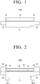
- FIG. 1 is a block diagram illustrating a light emitting diode (LED) apparatus 1000 according to an exemplary embodiment.
- an LED apparatus 1000 includes a light emitting diode 10, a light leakage preventing layer 20, a wavelength conversion layer 30, and a reflective layer 40.
- the light emitting diode 10 refers to a p-n junction diode that emits light from recombination of excess electron and hole pairs.
- the forward voltage is applied to the light emitting diode 10
- electrons in the n-type semiconductor layer meet with the holes of the p-type semiconductor layer and such recombining causes light emission.
- the light emitting diode 10 emits light when a voltage is applied, and the emitted light may fall incident on the wavelength conversion layer 30 to be described in greater detail below.
- the light emitting diode 10 emits blue light.
- exemplary embodiments are not limited thereto, and light of different colors may be emitted.
- the type of the wavelength conversion layer 30 may vary depending on the color of the light emitted by the light emitting diode 10.
- the type of the wavelength conversion layer 30 may vary depending on the color of the light to be finally emitted.
- the light leakage preventing layer 20 may be formed to surround the side surface of the light emitting diode 10 to prevent light emitted from the light emitting diode 10 from being emitted through the side surface of the light emitting diode 10.
- FIG. 1 the light leakage preventing layer 20 is shown only on the left and right sides of the light emitting diode 10.
- FIG. 1 is a cross-sectional view of the LED apparatus 1000, and accordingly, the light leakage preventing layer 20 may be formed so as to surround the side surface of the light emitting diode 10. This is also the same for the reflective layer 40 to be described in further detail below.
- the wavelength conversion layer 30 is formed on the light emitting diode 10 and may convert the wavelength of the light entering from the light emitting diode 10 and emit the resultant light.
- the wavelength conversion layer 30 may be a semiconductor layer that contains a quantum well layer.
- the quantum well layer emits energy when specific impurity electrons within the quantum well layer, which are excited by free electrons accelerated by the electric field, return to their original state.
- the light emitting diode 10 may also be manufactured in the same structure and emit light through the same operation. That is, the related quantum well layer may be a layer that emits light as current flows, which is also called 'electroluminescence'.
- electroluminescence it is possible to control the optical bandgap through the material type, the thickness and the doping process of the active layer using III-VI group semiconductor materials such as Ga, In and Al, thereby manufacturing an active layer having a structure that induces the single color such as blue, red and green.
- III-VI group semiconductor materials such as Ga, In and Al
- the wavelength conversion layer 30 includes a quantum well layer, it may act in a completely different way.
- the quantum well layer included in the wavelength conversion layer 30 acts not as electroluminescence but as photoluminescence.
- the wavelength conversion layer 30 includes a quantum well layer and may be formed of a semiconductor material.
- the wavelength conversion layer 30 may be a II-VI group semiconductor material, and may include a quantum well layer to which Zn, Se, Mg, and Cd are applied, for example.
- the photoluminescence effect can be improved.
- the wavelength conversion layer 30 may be formed through a semiconductor process such as deposition and patterning, such that a layer having a thinner and uniform thickness can be formed, unlike the case of using phosphors or quantum dots.
- the wavelength conversion layer 30 acts as a photoluminescence unlike the quantum well layer within the light emitting diode 10. That is, the wavelength conversion layer 30 may absorb the photons emitted from the light emitting diode 10 and emit energy as the specific impurity electrons in the quantum well layer are excited by the photons and return to their original state.
- the emitted energy is light
- the wavelength of the emitted light may be determined according to the material, thickness, etc. of the wavelength conversion layer 30.
- the wavelength conversion layer 30 emits light similarly to electroluminescence, it is also similar to the operation of photoluminescence in a sense that it is operated by incident light.
- the wavelength conversion layer 30 may be formed through a semiconductor process such as an MOCVD or MBE deposition process, so that the wavelength conversion layer 30 may be formed with an uniform thickness, which can in turn enhance the quality of emitted light.
- the wavelength conversion layer 30 may convert the first wavelength of light entering from the light emitting diode 10 into a predetermined second wavelength, and diffuse and emit the light of the second wavelength through the diffusion material to the outside.
- the wavelength conversion layer 30 may be one of a wavelength conversion layer corresponding to red (R) color, a wavelength conversion layer corresponding to green (G) color, a wavelength conversion layer corresponding to blue (B) color, and a wavelength conversion layer corresponding to white (W) color.
- R red
- G green
- B blue
- W white
- exemplary embodiments are not limited thereto, and the wavelength conversion layer 30 may be a wavelength conversion layer that emits different colors as needed.
- the reflective layer 40 is formed so as to surround the side surface of the wavelength conversion layer 30 to reflect the wavelength-converted light. That is, the reflective layer 40 allows the light emitted from the wavelength conversion layer 30 to be emitted only from one surface of the wavelength conversion layer 30, thereby increasing the brightness of the light.
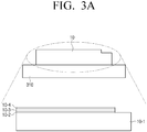
- FIG. 2 is a block diagram illustrating a detailed configuration of the LED apparatus 1000 according to an exemplary embodiment. The detailed description of the configuration shown in FIG. 2 that overlap the configuration shown in FIG. 1 will be omitted for the sake of brevity.
- the LED apparatus 1000 may further include a lower distributed Bragg reflector (DBR) coating layer 50, an upper DBR coating layer 60, an optical adhesive layer 70, a plurality of pads 80-1, 80- 2, and a substrate 90.
- DBR distributed Bragg reflector
- the lower DBR coating layer 50 may be formed between the light emitting diode 10 and the wavelength conversion layer 30.
- “in between” may be defined as in direct contact with these layers via an adhesive and in another embodiment, "in between” may include other layers there between such as an adhesive layer and perhaps some other layer.
- adhesive may or may not be viewed as a separate layer, depending on the terminology.
- the lower DBR coating layer 50 may pass the light of the first wavelength emitted from the light emitting diode 10, and reflect the light of the second wavelength wavelength-converted by the wavelength conversion layer 30.
- the upper DBR coating layer 60 may be formed on the wavelength conversion layer 30.
- “formed on” may be defined as in direct contact with the wavelength conversion layer 30 and in another embodiment, “formed on” may include other layers therein between such as an adhesive layer.
- the upper DBR coating layer 60 may pass light of the second wavelength wavelength-converted by the wavelength conversion layer 30, and reflect light of wavelengths other than the second wavelength.
- the LED apparatus 1000 may emit high-purity light by the lower DBR coating layer 50 and the upper DBR coating layer 60.
- the lower DBR coating layer 50 and the upper DBR coating layer 60 may be formed through a semiconductor process such as CVD in the same manner as the wavelength conversion layer 30.
- the upper DBR coating layer 60, the wavelength conversion layer 30, and the lower DBR coating layer 50 may be sequentially deposited on the substrate through CVD process, and separated from the substrate and attached to the upper portion of the light emitting diode 10. That is, the upper DBR coating layer 60, the wavelength conversion layer 30, and the lower DBR coating layer 50 may be formed on a substrate separate from the light emitting diode 10 through a semiconductor process.
- the upper DBR coating layer 60, the wavelength conversion layer 30, and the lower DBR coating layer 50, and the like are collectively referred to as wavelength converting materials.
- an optical adhesive layer 70 may be used to bond the light emitting diode 10 and the wavelength converting material. That is, the optical adhesive layer 70 between the light emitting diode 10 and the lower DBR coating layer 50 may bond the light emitting diode 10 and the lower DBR coating layer 50.
- the optical adhesive layer 70 may be a transparent material capable of transmitting light.
- a method for manufacturing a wavelength converting material using a separate substrate will be described in further detail below.
- a plurality of pads 80-1, 80-2 may be formed under the light emitting diode 10 to receive external power.
- the plurality of pads 80-1, 80-2 may receive external power and apply voltage to the light emitting diode 10.
- Each of the plurality of pads 80-1, 80-2 may be connected to each of the p-type semiconductor layer and the n-type semiconductor layer of the light emitting diode 10 to apply voltage thereto.
- the substrate 90 may be the remaining structure that is not removed in the manufacturing process, and may be in such a form that it surrounds the side surface of the wavelength converting material.
- the substrate 90 may be particularly useful for a structure that includes a plurality of connected LED apparatuses 1000.
- the substrate 90 is shown only on the left and right sides of the wavelength converting materials. However, this is only because FIG. 2 is a cross-sectional view of the LED apparatus 1000, and accordingly, the substrate 90 may be formed so as to surround the side surface of the wavelength converting materials.
- the wavelength conversion layers 30 can be uniformly manufactured, and accordingly, the quality of the light emitted from the LED apparatus 1000 can be enhanced.
- a semiconductor material layer may be formed in a growth chamber using metal-organic vapor deposition (MOCVD) method or molecular beam epitaxy (MBE) method, and may be deposited by various methods such as PECVD, APCVD, LPCVD, UHCVD, PVD, electron beam method, resistance heating method, and so on.
- MOCVD metal-organic vapor deposition
- MBE molecular beam epitaxy
- the light emitting diode 10 may be formed on a base substrate 310.
- an n-type semiconductor layer 10-1 may be stacked on the base substrate 310
- a quantum well layer 10-2 may be stacked on the n-type semiconductor layer 10-1
- a p-type semiconductor layer 10-3 may be stacked on the quantum well layer 10-2
- an indium tin oxide (ITO) layer may be stacked on the p-type semiconductor layer 10-3.
- the base substrate 310 may be made of a material such as glass, Si, InP, GaAs, and so on.
- the area of each of the n-type semiconductor layer 10-1, the quantum well layer 10-2, the p-type semiconductor layer 10-3, and the ITO 10-4 layer may be the same as the area of the base substrate 310.
- FIG. 3A showing the light emitting diode 10, a certain region of the n-type semiconductor layer 10-1, the quantum well layer 10-2, the p-type semiconductor layer 10-3, and the ITO layer 10-4 may be etched. Since the etching method is well known technology, this will not be redundantly explained.
- the n-type semiconductor layer 10-1 is longer than the quantum well layer 10-2, the p-type semiconductor layer 10-3, and the ITO layer 10-4 so that the light emitting diode 10 has a concave edge.
- the substrate 310 may be longer than the light emitting diode 10 to accommodate for subsequent layers that may be added to the sides of the light emitting diode 10.
- the n-type semiconductor layer 10-1 and the p-type semiconductor layer 10-3 may be stacked as GaN.
- the ITO layer 10-4 is a transparent conductive film having electrical conductivity, and it can reduce electrical resistance.
- the light emitting diode 10 may be a material that emits blue light. However, exemplary embodiments are not limited thereto, and any light emitting diode 10 may be used as long as it can emit light.
- the light leakage preventing layer 20 may be formed so as to surround the side surface of the light emitting diode 10.
- the light leakage preventing layer 20 may prevent light emitted from the light emitting diode 10 from being emitted through the side surface of the light emitting diode 10.
- the light leakage preventing layer 20 is shown to surround only one side surface of the light emitting diode 10
- the light leakage preventing layer may surround one or more of the side surfaces of the light emitting diode 10 and may surround these side surfaces in their entirety or with a portion of the side surface of the light emitting diode 10 not being covered such as layers 10-2 through 10-4 shown in Fig. 3A .
- the region in the base substrate 310 that corresponds to the light emitting diode 10 may be etched.
- the region corresponding to the light emitting diode 10' it means the lower region of the light emitting diode 10 in the base substrate 310. Since the method of etching the base substrate 310 is already known technique, specific description thereof will be omitted.
- the substrate 90 of FIG. 2 may be formed.
- the base substrate 310 is shown as being etched.
- exemplary embodiments are not limited thereto.
- the region corresponding to the light emitting diode 10 in the base substrate 310 may be etched more deeply to further etch a certain region of the light emitting diode 10.
- the wavelength converting material may be bonded to the exposed region of the light emitting diode 10 that is exposed as the base substrate 310 is etched. Meanwhile, the wavelength converting material is fabricated using a substrate other than the base substrate 310, as will be described in further detail below with reference to the drawings.
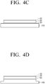
- FIGS. 4A to 4E are views illustrating a method of forming a wavelength converting material on another substrate 410 ('second substrate'), in which the wavelength converting material may include a semiconductor layer including a quantum well layer, according to an exemplary embodiment.
- the upper DBR coating layer 60 may be formed on the second substrate 410 through CVD process.
- the second substrate 410 may be made of a material such as glass, Si, InP, GaAs, and so on.
- the wavelength conversion layer 30 may be formed on the upper DBR coating layer 60 through CVD process.
- the wavelength conversion layer 30 may be a semiconductor layer that includes a quantum well layer.
- the wavelength conversion layer 30 is a II-VI group semiconductor material and may be one of a wavelength conversion layer corresponding to a red (R) color, a wavelength conversion layer corresponding to a green (G) color, a wavelength conversion layer corresponding to a blue (B) color, and a wavelength conversion layer corresponding to a white (W) color.
- the region other than the region corresponding to the light emitting diode 10 in the second substrate 410 may be etched.
- the region other than the region corresponding to the light emitting diode 10 in the second substrate 410 may be removed with a photolithography process or a transfer process using a glass mold.
- the upper DBR coating layer 60, the wavelength conversion layer 30, and the lower DBR coating layer 50 in a size corresponding to the area of the light emitting diode 10, it is possible to etch only a certain region of the second substrate 410, thus forming the etched second substrate 420, as shown in FIG. 4D .
- the upper DBR coating layer 60, the wavelength conversion layer 30, and the lower DBR coating layer 50 may initially be formed to have a size corresponding to the area of the second substrate 410.
- a certain region of each of the upper DBR coating layer 60, the wavelength conversion layer 30, and the lower DBR coating layer 50 as well as a certain region of the second substrate 410 may also be etched.
- a reflective layer 40 is formed, surrounding the side surface of the wavelength converting material and extending by a predetermined length from the side surface of the wavelength converting material to a lower portion of the lower DBR coating layer.
- the reflective layer 40 is formed so as to surround the side surface of the wavelength conversion layer 30.
- the reflective layer 40 may cover the entire side surfaces of the wavelength conversion layer 30 and additionally extends so as to cover a portion of the lower DBR coating layer 50, as shown in FIG. 4E .
- the manufacturing process of FIG. 3 is described as being followed by the manufacturing process of FIG. 4 .
- the manufacturing process of FIG. 3 and the manufacturing process of FIG. 4 are not limited to a certain sequence, and accordingly, any of them may be performed first.
- the wavelength converting material of FIG. 4 may be bonded to the lower portion of the light emitting diode 10 of FIG. 3 , which will be described in further detail below with reference to the drawings.
- FIG. 5A is a view illustrating that the optical adhesive layer 70 is formed on the lower surface of the lower DBR coating layer 50.
- the optical adhesive layer 70 is formed on one of the lower surface of the light emitting diode 10 and the lower surface of the lower DBR coating layer, to bond the wavelength converting material to the lower portion of the light emitting diode 10.
- any method for bonding a wavelength converting material to the lower portion of the light emitting diode 10 may be used.
- epoxy based on thermal deformation may be utilized.
- a method involves forming a specific layer between the light emitting diode 10 and the wavelength converting material, then the specific layer formed has to be transparent.
- a plurality of pads 80-1, 80-2 may be formed under the light emitting diode 10 to receive external power.
- the time of forming the plurality of pads 80-1, 80-2 is not strictly limited.
- the plurality of pads 80-1, 80-2 may have been formed in the light emitting diode 10 before the wavelength converting material is bonded to the lower portion of the light emitting diode 10.
- the lower DBR coating layer 50 and the upper DBR coating layer 60 are shown as being included, but this is only an example.
- the wavelength converting material may include only the wavelength conversion layer 30 and the reflective layer 40 without including the lower DBR coating layer 50 and the upper DBR coating layer 60.
- the wavelength conversion layer may convert a first wavelength of the light entering from the light emitting diode 10 into a predetermined second wavelength, and diffuse and emit the light of the second wavelength through the diffusion material
- the lower DBR coating layer 50 pass the light of the first wavelength emitted from the light emitting diode 10 and reflect the light of the second wavelength that is wavelength-converted by the wavelength conversion layer 30, and the upper DBR coating layer 60 pass the light of the second wavelength and reflect light of the wavelength other than the second wavelength
- the reflective layer 40 may reflect the wavelength-converted light emitted through the side surface and the lower portion of the wavelength converting material. Accordingly, it is possible to improve the quality of light emitted from the LED apparatus 1000.
- the wavelength conversion layer 30 may be formed with a uniform thickness as it is manufactured through a semiconductor process, the wavelength of the light emitted from the LED apparatus 1000 can be uniform.
- FIGS. 6A and 6B are views illustrating a plurality of packaged LED apparatuses 1000 according to an embodiment.
- the first wavelength conversion layer 610 may be a wavelength conversion layer corresponding to a red (R) color
- the second wavelength conversion layer 620 may be a wavelength conversion layer corresponding to a green (G) color
- the third wavelength conversion layer 630 may be a wavelength conversion layer corresponding to a blue (B) color.
- R red
- G green
- B blue
- Such configuration may be used as one pixel, according to an exemplary embodiment.
- the method of manufacturing the above-described configuration may also use the methods of FIGS. 3A to 5C .
- the method of FIGS. 3A to 3C may be modified such that a plurality of light emitting diodes may be formed on a one substrate.
- a single substrate may be used to manufacture a plurality of light emitting diodes such as the three light emitting diodes of different colors described above.
- the method of FIGS. 4A to 4E may also be modified such that a plurality of wavelength converting materials may be formed on one other substrate.
- a single substrate may be used to manufacture a plurality of wavelength converting materials respectively corresponding to the light emitting diodes such that one wavelength converting material corresponds to one respective light emitting diode.
- the plurality of wavelength converting materials may have different materials in order to emit different color lights.
- a plurality of packaged LED apparatuses 1000 as shown in FIG. 6A may be manufactured by bonding the one substrate to a second substrate and then removing the second substrate.
- the entire plurality of LED apparatuses 1000 being packaged as shown in FIG. 6A may form one pixel, and each of the LED apparatuses of the plurality of LED apparatuses 1000 in package may operate as a subpixel.
- a plurality of wavelength converting materials of the same material may be formed using the method described above, and then diced into a plurality of LED apparatuses 1000.
- the first wavelength conversion layer 610, the second wavelength conversion layer 620, and the third wavelength conversion layer 630 may all be formed of the same material to manufacture a package of a plurality of LED apparatuses 1000 that emits a monochromatic color light.
- FIG. 6A shows the LED apparatus 1000 only, while omitting illustration of some other configurations and most of the reference drawings.
- a plurality of packaged LED apparatuses 1000 may include all configurations described above. That is, the plurality of packaged LED apparatus 1000 may include light emitting diodes 10-1, 10-2, 10-3, a light leakage preventing layer 20, wavelength conversion layers 610, 620, 630, reflective layers 40-1, 40-2, 40-3, lower DBR coating layers 50-1, 50-2, 50-3, upper DBR coating layers 60-1, 60-2, 60-3, optical adhesive layers 70-1, 70-2, 70-3, a plurality of pads 80-1, 80-2, 80-3, 80-4, 80-5, 80-6, and a substrate 90.
- the plurality of packaged LED apparatus 1000 may include light emitting diodes 10-1, 10-2, 10-3, a light leakage preventing layer 20, wavelength conversion layers 610, 620, 630, reflective layers 40-1, 40-2, 40-3, lower DBR coating layers 50-1, 50-2, 50-3, upper DBR coating layers 60-1, 60-2, 60-3, optical adhesive layers 70-1, 70-2, 70-3, a plurality of pads 80-1
- each of the wavelength conversion layers 610, 620, 630 may be a wavelength conversion layer corresponding to a red (R) color, a wavelength conversion layer corresponding to a green (G) color, and a wavelength conversion layer corresponding to a blue (B) color
- the lower DBR coating layers 50-1, 50-2, 50-3 and the upper DBR coating layers 60-1, 60-2, 60-3 may be formed to correspond to the adjacent wavelength conversion layers.
- the lower DBR coating layer 50-1 may pass the light of a first wavelength emitted from the light emitting diode 10-1, and reflect the second wavelength (i.e., wavelength corresponding to the R color) that is wavelength-converted by the wavelength conversion layer 610.
- the upper DBR coating layer 60-1 may pass the light of the second wavelength (wavelength corresponding to the R color) that is wavelength-converted by the wavelength conversion layer 610 and reflect the light of wavelengths other than the second wavelength (i.e., wavelength corresponding to the R color).
- a light emitting diode is formed on the substrate, in operation S710.
- the light leakage preventing layer is formed so as to surround the side surface of the light emitting diode, in operation S720.
- the region corresponding to the light emitting diode in the substrate is etched, in operation S730.
- a wavelength converting material including a semiconductor layer including a quantum well layer is bonded to the lower portion of the light emitting diode in the etched region, in operation S740.
- the semiconductor layer including a quantum well layer may be an inorganic semiconductor layer.
- the method may additionally include generating a wavelength converting material, which may include: forming an upper distributed Bragg reflector (DBR) coating layer on another substrate ('second substrate') through deposition process; forming a wavelength conversion layer on the upper DBR coating layer through CVD process; forming a lower DBR coating layer on the wavelength conversion layer through the CVD process; and etching the region of the second substrate other than the region corresponding to the light emitting diode, and bonding in operation S740 may include bonding the wavelength converting material to a lower portion of the light emitting diode so that the lower DBR coating layer is bonded to the lower surface of the light emitting diode.
- a wavelength converting material may include: forming an upper distributed Bragg reflector (DBR) coating layer on another substrate ('second substrate') through deposition process; forming a wavelength conversion layer on the upper DBR coating layer through CVD process; forming a lower DBR coating layer on the wavelength conversion layer through the CVD process; and etching the region of the second substrate
- the upper DBR coating layer, the wavelength conversion layer, and the lower DBR coating layer may be formed to have a size corresponding to the area of the light emitting diode.
- the method may additionally include removing the second substrate included in the wavelength converting material.
- forming the wavelength converting material may additionally include forming a reflective layer, which surrounds the side surface of the wavelength converting material and is extended by a predetermined length from the side surface of the wavelength converting material to a lower portion of the lower DBR coating layer.
- the light leakage preventing layer may prevent light emitted from the light emitting diode from being emitted through the side surface of the light emitting diode
- the wavelength conversion layer may convert a first wavelength of light entering from the light emitting diode to a predetermined second wavelength and diffuse and emit the light of the second wavelength to the outside through a diffusion material
- the lower DBR coating layer may pass the light of the first wavelength emitted from the light emitting diode and reflect the light of the second wavelength that is wavelength-converted by the wavelength conversion layer
- the upper DBR coating layer may pass the light of the second wavelength and reflect the light of a wavelength other than the second wavelength
- the reflective layer may reflect the wavelength-converted light emitted through the side surface and the lower portion of the wavelength converting material.
- the bonding in operation S740 may include forming an optical adhesive layer on one of the lower surface of the light emitting diode and the lower surface of the lower DBR coating layer to bond the wavelength converting material to a lower portion of the light emitting diode.
- the wavelength conversion layer may be one of a wavelength conversion layer corresponding to red (R) color, a wavelength conversion layer corresponding to green (G) color, a wavelength conversion layer corresponding to blue (B) color, and a wavelength conversion layer corresponding to white (W) color.
- the method may further include forming a plurality of pads under the light emitting diode to receive external power.
- the wavelength conversion layer may be a II-VI group semiconductor material.
- a semiconductor manufacturing process may be used so that the size of the LED apparatus can be further reduced (e.g., to 10 ⁇ m or below), while uniform optical performance is ensured.
- the transmittance, color gamut and color purity can be improved as compared with the related examples using materials such as phosphors or quantum dots.
- the layer is described as being formed through the CVD process, exemplary embodiments are not limited thereto.
- the layer may be formed through a growing process.
Landscapes
- Led Device Packages (AREA)
- Engineering & Computer Science (AREA)
- Power Engineering (AREA)
- Microelectronics & Electronic Packaging (AREA)
- Led Devices (AREA)
- Physics & Mathematics (AREA)
- Condensed Matter Physics & Semiconductors (AREA)
- General Physics & Mathematics (AREA)
- Computer Hardware Design (AREA)
Claims (14)
- Herstellungsverfahren einer Leuchtdioden-(LED)-Vorrichtung (1000), umfassend:Bilden einer LED (10) auf einem Substrat (310);Bilden einer Lichtaustrittsverhinderungsschicht (20), die mindestens eine Seitenfläche der LED (10) umgibt;Ätzen eines Abschnitts des Substrats (310), der der LED (10) entspricht; undVerbinden eines Wellenlängenumwandlungsmaterials mit der LED (10) in dem geätzten Abschnitt,wobei das Wellenlängenumwandlungsmaterial eine Wellenlängenumwandlungs-Halbleiterschicht (30) und eine reflektierende Schicht (40) umfasst,wobei die Wellenlängenumwandlungs-Halbleiterschicht (30) eine Quantentopfschicht umfasst, um ein von der LED (10) emittiertes Licht in ein wellenlängenkonvertiertes Licht umzuwandeln,wobei die reflektierende Schicht (40) mindestens eine Seitenfläche der Wellenlängenumwandlungs-Halbleiterschicht (30) umgibt, um das wellenlängenumgewandelte Licht an der mindestens einen Seitenfläche der Wellenlängenumwandlungs-Halbleiterschicht (30) zu reflektieren, undwobei sich die reflektierende Schicht (40) auf einen Abschnitt einer Oberfläche der Wellenlängenumwandlungs-Halbleiterschicht (30) erstreckt, die der LED (10) zugewandt ist, um das wellenlängenkonvertierte Licht an dem der LED (10) zugewandten Abschnitt der Oberfläche der Wellenlängenumwandlungs-Halbleiterschicht (30) zu reflektieren.
- Herstellungsverfahren nach Anspruch 1, ferner umfassend das Erzeugen des Wellenlängenumwandlungsmaterials, wobei das Erzeugen des Wellenlängenumwandlungsmaterials Folgendes umfasst:Bilden einer oberen verteilten Bragg-Reflektor-(DBR)-Beschichtungsschicht (60) auf einem anderen Substrat (420) durch einen chemischen Dampfabscheidungs-(CVD)-Prozess;Bilden der Wellenlängenumwandlungs-Halbleiterschicht (30) auf der oberen DBR-Beschichtungsschicht (60) durch den CVD-Prozess;Bilden einer unteren DBR-Beschichtungsschicht (50) auf der Wellenlängenumwandlungs-Halbleiterschicht (30) durch den CVD-Prozess; undÄtzen eines anderen Bereichs des anderen Substrats (420) als der der LED entsprechenden Bereich,wobei das Verbinden das Verbinden des Wellenlängenumwandlungsmaterials mit der LED (10) umfasst, so dass die LED (10) und die untere DBR-Beschichtungsschicht (50) miteinander verbunden werden.
- Herstellungsverfahren nach Anspruch 2, wobei die obere DBR-Beschichtungsschicht (60), die Wellenlängenumwandlungs-Halbleiterschicht (30) und die untere DBR-Beschichtungsschicht (50) mit einer Größe entsprechend einer Größe der LED gebildet werden (10).
- Herstellungsverfahren nach Anspruch 2 oder 3, ferner umfassend, nach dem Verbinden des Wellenlängenumwandlungsmaterials mit der LED (10), das Entfernen des anderen Substrats (420), das in dem Wellenlängenumwandlungsmaterial enthalten ist.
- Herstellungsverfahren nach einem der Ansprüche 2 bis 4, wobei die reflektierende Schicht (40) gebildet wird, so dass sie sich auch um eine vorbestimmte Länge von der mindestens einen Seitenfläche des Wellenlängenumwandlungsmaterials zum unteren Abschnitt der unteren DBR-Beschichtungsschicht (50) erstreckt.
- Herstellungsverfahren nach Anspruch 5, wobei die Lichtaustrittsverhinderungsschicht (20) verhindert, dass von der LED (10) emittiertes Licht durch die mindestens eine Seitenfläche der LED (10) emittiert wird,die Wellenlängenumwandlungs-Halbleiterschicht (30) eine erste Wellenlänge des von der LED (10) emittierten Lichts in eine vorbestimmte zweite Wellenlänge umwandelt und das Licht der zweiten Wellenlänge durch ein Diffusionsmaterial nach außen streut und emittiert, die untere DBR-Beschichtungsschicht (50) das von der LED (10) emittierte Licht der ersten Wellenlänge durchlässt und das Licht der zweiten Wellenlänge reflektiert, das durch die Wellenlängenumwandlungs-Halbleiterschicht (30) wellenlängenkonvertiert wird, die obere DBR-Beschichtungsschicht (60) das Licht der zweiten Wellenlänge durchlässt und das Licht einer anderen Wellenlänge als der zweiten Wellenlänge reflektiert, unddie reflektierende Schicht (40) das durch die mindestens eine Seitenfläche und eine untere Fläche des Wellenlängenumwandlungsmaterials emittierte Licht reflektiert.
- Herstellungsverfahren nach einem der Ansprüche 2 bis 6, wobei das Verbinden das Bilden einer optischen Klebeschicht (70) auf einer von der LED (10) oder der unteren DBR-Beschichtungsschicht (50) umfasst, um das Wellenlängenumwandlungsmaterial an den unteren Abschnitt der Leuchtdiode (10) zu verbinden.
- Herstellungsverfahren nach einem der Ansprüche 1 bis 7, wobei die Wellenlängenumwandlungs-Halbleiterschicht (30) eine der folgenden ist: eine erste Wellenlängenumwandlungs-Halbleiterschicht (610), die einer roten (R) Farbe entspricht; eine zweite Wellenlängenumwandlungs-Halbleiterschicht (620), die einer grünen (G) Farbe entspricht; eine dritte Wellenlängenumwandlungs-Halbleiterschicht (630), die einer blauen (B) Farbe entspricht; und eine vierte Wellenlängenumwandlungs-Halbleiterschicht, die einer weißen Farbe (W) entspricht.
- Herstellungsverfahren nach einem der Ansprüche 1 bis 8, ferner umfassend das Bilden einer Vielzahl von Anschlussflächen (80-1, 80-2, 80-3, 80-4, 80-5, 80-6) unter der LED (10), um externe Energie zu erhalten.
- Herstellungsverfahren nach einem der Ansprüche 1 bis 9, wobei die Wellenlängenumwandlungs-Halbleiterschicht (30) eine Halbleiterschicht der Gruppe II-VI ist.
- Leuchtdioden-(LED)-Vorrichtung (1000), umfassend:eine LED (10), die konfiguriert ist, um Licht zu emittieren;eine Lichtaustrittsverhinderungsschicht (20), die so ausgebildet ist, dass sie mindestens eine Seitenfläche der LED (10) umgibt;ein Wellenlängenumwandlungsmaterial, das auf der LED (10) gebildet ist, wobei das Wellenlängenumwandlungsmaterial eine Wellenlängenumwandlungs-Halbleiterschicht (30) und eine reflektierende Schicht (40) umfasst, wobei die Wellenlängenumwandlungs-Halbleiterschicht (30) eine Quantentopfschicht umfasst, um das von der LED (10) emittierte Licht in ein wellenlängenkonvertiertes Licht umzuwandeln;wobei die reflektierende Schicht (40) mindestens eine Seitenfläche der Wellenlängenumwandlungs-Halbleiterschicht (30) umgibt, um das wellenlängenkonvertierte Licht an der mindestens einen Seitenfläche der Wellenlängenumwandlungs-Halbleiterschicht (30) zu reflektieren, undwobei sich die reflektierende Schicht (40) auf einen Abschnitt einer Oberfläche der Wellenlängenumwandlungs-Halbleiterschicht (30) erstreckt, die der LED (10) zugewandt ist, um das wellenlängenkonvertierte Licht zu reflektieren, das durch den der LED (10) zugewandten Abschnitt der Oberfläche der Wellenlängenumwandlungs-Halbleiterschicht (30) emittiert wird.
- LED-Vorrichtung (1000) nach Anspruch 11, wobei das Wellenlängenumwandlungsmaterial ferner eine untere verteilte Bragg-Reflektor(DBR)-Beschichtungsschicht (50) umfasst, die zwischen der LED (10) und der Wellenlängenumwandlungs-Halbleiterschicht (30) gebildet ist,
wobei die untere DBR-Beschichtungsschicht (50) das von der LED (10) emittierte Licht einer ersten Wellenlänge durchlässt und das Licht einer zweiten Wellenlänge reflektiert, das durch die Wellenlängenumwandlungs-Halbleiterschicht (30) wellenlängenkonvertiert wird. - LED-Vorrichtung (1000) nach Anspruch 12, wobei das Wellenlängenumwandlungsmaterial ferner eine obere DBR-Beschichtungsschicht (60) umfasst, die auf der Wellenlängenumwandlungs-Halbleiterschicht (30) gebildet ist,
wobei die obere DBR-Beschichtungsschicht (60) das Licht der zweiten Wellenlänge durchlässt und das Licht einer anderen Wellenlänge als der zweiten Wellenlänge reflektiert. - LED-Vorrichtung (1000) nach einem der Ansprüche 12 bis 13, ferner umfassend eine optische Klebeschicht (70), die zwischen der LED (10) und der unteren DBR-Beschichtungsschicht (50) gebildet ist.
Applications Claiming Priority (1)
| Application Number | Priority Date | Filing Date | Title |
|---|---|---|---|
| KR1020170134562A KR102384731B1 (ko) | 2017-10-17 | 2017-10-17 | Led 장치 및 그 제조 방법 |
Publications (2)
| Publication Number | Publication Date |
|---|---|
| EP3496142A1 EP3496142A1 (de) | 2019-06-12 |
| EP3496142B1 true EP3496142B1 (de) | 2021-11-03 |
Family
ID=61256586
Family Applications (1)
| Application Number | Title | Priority Date | Filing Date |
|---|---|---|---|
| EP18157661.2A Active EP3496142B1 (de) | 2017-10-17 | 2018-02-20 | Leuchtdiodenvorrichtung und herstellungsverfahren |
Country Status (5)
| Country | Link |
|---|---|
| US (2) | US10818826B2 (de) |
| EP (1) | EP3496142B1 (de) |
| KR (1) | KR102384731B1 (de) |
| CN (1) | CN111133593B (de) |
| WO (1) | WO2019078430A1 (de) |
Families Citing this family (5)
| Publication number | Priority date | Publication date | Assignee | Title |
|---|---|---|---|---|
| DE102019115351A1 (de) * | 2019-06-06 | 2020-12-10 | OSRAM Opto Semiconductors Gesellschaft mit beschränkter Haftung | Halbleiterbauelement mit Strahlungskonversionselement und Verfahren zum Herstellen von Strahlungskonversionselementen |
| KR102436024B1 (ko) * | 2020-02-26 | 2022-08-24 | 주식회사 케이티앤지 | 광학 모듈 및 이를 포함하는 에어로졸 생성 장치 |
| CN114335291B (zh) * | 2020-09-30 | 2024-02-02 | Tcl科技集团股份有限公司 | 一种发光元件及其制备方法、光源板 |
| US20220165923A1 (en) * | 2020-11-24 | 2022-05-26 | Creeled, Inc. | Cover structure arrangements for light emitting diode packages |
| WO2025097307A1 (zh) * | 2023-11-07 | 2025-05-15 | 京东方科技集团股份有限公司 | 发光装置及其制作方法、显示面板、显示装置 |
Family Cites Families (19)
| Publication number | Priority date | Publication date | Assignee | Title |
|---|---|---|---|---|
| US8481977B2 (en) * | 2006-03-24 | 2013-07-09 | Goldeneye, Inc. | LED light source with thermally conductive luminescent matrix |
| US9018619B2 (en) | 2006-10-09 | 2015-04-28 | Cree, Inc. | Quantum wells for light conversion |
| KR20100077191A (ko) * | 2007-10-08 | 2010-07-07 | 쓰리엠 이노베이티브 프로퍼티즈 컴파니 | 접합된 반도체 파장 변환기를 갖는 발광 다이오드 |
| US8081289B2 (en) | 2008-08-06 | 2011-12-20 | Universal Optoelectronics Co., Ltd. | Enhanced wavelength-converting structure |
| KR20110053376A (ko) * | 2008-09-04 | 2011-05-20 | 쓰리엠 이노베이티브 프로퍼티즈 컴파니 | Gan ld에 의해 광학적으로 펌핑되는 히트 싱크 상의 ⅱ-ⅵ족 mqw vcsel |
| US20100244065A1 (en) * | 2009-03-30 | 2010-09-30 | Koninklijke Philips Electronics N.V. | Semiconductor light emitting device grown on an etchable substrate |
| JP5292368B2 (ja) | 2010-08-27 | 2013-09-18 | 株式会社朝日ラバー | 発光色変換シートおよびそれを用いた発光装置 |
| KR20140046419A (ko) | 2011-05-16 | 2014-04-18 | 베르라세 테크놀러지스 엘엘씨 | 공진기가 향상된 광전자 장치 및 그 제조 방법 |
| KR101330176B1 (ko) | 2011-08-24 | 2013-11-15 | 삼성전자주식회사 | 발광소자 및 그 제조방법 |
| US8796665B2 (en) * | 2011-08-26 | 2014-08-05 | Micron Technology, Inc. | Solid state radiation transducers and methods of manufacturing |
| WO2015011590A1 (en) | 2013-07-22 | 2015-01-29 | Koninklijke Philips N.V. | Flip-chip side emitting led |
| EP3111487B1 (de) * | 2014-02-27 | 2020-03-11 | Lumileds Holding B.V. | Verfahren zur herstellung einer vorrichtung zur emission von wellenlängenumgewandeltem licht |
| KR101520743B1 (ko) | 2014-05-16 | 2015-05-18 | 코닝정밀소재 주식회사 | 발광 다이오드 패키지 제조방법 |
| DE102014107472A1 (de) * | 2014-05-27 | 2015-12-03 | Osram Opto Semiconductors Gmbh | Halbleiterbauelement und Beleuchtungsvorrichtung |
| KR20170005317A (ko) | 2015-07-03 | 2017-01-12 | 삼성전자주식회사 | 반도체 발광소자 |
| KR102415331B1 (ko) | 2015-08-26 | 2022-06-30 | 삼성전자주식회사 | 발광 소자 패키지, 및 이를 포함하는 장치 |
| US10211384B2 (en) | 2016-03-28 | 2019-02-19 | Samsung Electronics Co., Ltd. | Light emitting diode apparatus and manufacturing method thereof |
| KR102464931B1 (ko) * | 2016-03-28 | 2022-11-09 | 삼성전자주식회사 | Led 장치 및 그 제조 방법 |
| KR102480220B1 (ko) * | 2016-04-08 | 2022-12-26 | 삼성전자주식회사 | 발광 다이오드 모듈 및 이를 구비한 디스플레이 패널 |
-
2017
- 2017-10-17 KR KR1020170134562A patent/KR102384731B1/ko active Active
-
2018
- 2018-02-20 EP EP18157661.2A patent/EP3496142B1/de active Active
- 2018-02-26 US US15/904,876 patent/US10818826B2/en active Active
- 2018-04-02 CN CN201880060577.8A patent/CN111133593B/zh active Active
- 2018-04-02 WO PCT/KR2018/003853 patent/WO2019078430A1/en not_active Ceased
-
2020
- 2020-10-06 US US17/063,753 patent/US11424392B2/en active Active
Non-Patent Citations (1)
| Title |
|---|
| None * |
Also Published As
| Publication number | Publication date |
|---|---|
| US10818826B2 (en) | 2020-10-27 |
| EP3496142A1 (de) | 2019-06-12 |
| WO2019078430A1 (en) | 2019-04-25 |
| US20210020811A1 (en) | 2021-01-21 |
| US11424392B2 (en) | 2022-08-23 |
| KR20190042913A (ko) | 2019-04-25 |
| KR102384731B1 (ko) | 2022-04-08 |
| CN111133593B (zh) | 2023-08-25 |
| CN111133593A (zh) | 2020-05-08 |
| US20190115506A1 (en) | 2019-04-18 |
Similar Documents
| Publication | Publication Date | Title |
|---|---|---|
| US11424392B2 (en) | Light emitting diode apparatus and manufacturing method thereof | |
| US6744196B1 (en) | Thin film LED | |
| KR102131599B1 (ko) | 발광 다이오드 및 그 제조 방법 | |
| US6841802B2 (en) | Thin film light emitting diode | |
| KR101138952B1 (ko) | 복수개의 발광셀들을 갖는 웨이퍼 레벨 발광 다이오드 패키지 및 그것을 제조하는 방법 | |
| KR102797522B1 (ko) | 반도체 발광 소자 및 이의 제조 방법 | |
| US9780260B2 (en) | Semiconductor light emitting device and manufacturing method of the same | |
| US20160365702A1 (en) | Crystalline color-conversion device | |
| KR20150021235A (ko) | 표시장치 | |
| KR20170142022A (ko) | 표시 장치 및 이의 제조 방법 | |
| JP2014158024A (ja) | 発光素子パッケージ及びその製造方法 | |
| US20260018569A1 (en) | Light emitting device and led display apparatus including the same | |
| KR20130030283A (ko) | 복수개의 발광셀들을 갖는 발광 다이오드 패키지 및 그것을 제조하는 방법 | |
| US8637893B2 (en) | Light emitting device package, method of manufacturing the same, and lighting system | |
| KR20120031473A (ko) | 복수개의 발광셀들을 갖는 웨이퍼 레벨 발광 다이오드 패키지 및 그것을 제조하는 방법 | |
| US11948922B2 (en) | Light emitting device and LED display apparatus including the same | |
| KR101420214B1 (ko) | 질화물계 발광 소자 | |
| JP5264935B2 (ja) | オプトエレクトロニクス部品およびその製造方法 | |
| CN116960146A (zh) | 发光器件和发光器件的制备方法 | |
| KR20190106600A (ko) | 발광 소자 패키지 및 그 제조 방법 | |
| KR20110107619A (ko) | 반도체 발광소자 및 그 제조방법, 이를 이용한 패키지 | |
| KR100670929B1 (ko) | 플립칩 구조의 발광 소자 및 이의 제조 방법 | |
| KR20130043858A (ko) | 발광소자와 발광 어레이, 및 각각의 제조방법 | |
| KR102628787B1 (ko) | 발광 소자 |
Legal Events
| Date | Code | Title | Description |
|---|---|---|---|
| PUAI | Public reference made under article 153(3) epc to a published international application that has entered the european phase |
Free format text: ORIGINAL CODE: 0009012 |
|
| STAA | Information on the status of an ep patent application or granted ep patent |
Free format text: STATUS: THE APPLICATION HAS BEEN PUBLISHED |
|
| AK | Designated contracting states |
Kind code of ref document: A1 Designated state(s): AL AT BE BG CH CY CZ DE DK EE ES FI FR GB GR HR HU IE IS IT LI LT LU LV MC MK MT NL NO PL PT RO RS SE SI SK SM TR |
|
| AX | Request for extension of the european patent |
Extension state: BA ME |
|
| STAA | Information on the status of an ep patent application or granted ep patent |
Free format text: STATUS: REQUEST FOR EXAMINATION WAS MADE |
|
| 17P | Request for examination filed |
Effective date: 20190910 |
|
| RBV | Designated contracting states (corrected) |
Designated state(s): AL AT BE BG CH CY CZ DE DK EE ES FI FR GB GR HR HU IE IS IT LI LT LU LV MC MK MT NL NO PL PT RO RS SE SI SK SM TR |
|
| STAA | Information on the status of an ep patent application or granted ep patent |
Free format text: STATUS: EXAMINATION IS IN PROGRESS |
|
| 17Q | First examination report despatched |
Effective date: 20200416 |
|
| REG | Reference to a national code |
Ref country code: DE Ref legal event code: R079 Ref document number: 602018025950 Country of ref document: DE Free format text: PREVIOUS MAIN CLASS: H01L0025075000 Ipc: H01L0033500000 |
|
| RIC1 | Information provided on ipc code assigned before grant |
Ipc: H01L 33/00 20100101ALI20210623BHEP Ipc: H01L 33/20 20100101ALI20210623BHEP Ipc: H01L 33/46 20100101ALI20210623BHEP Ipc: H01L 33/50 20100101AFI20210623BHEP |
|
| GRAP | Despatch of communication of intention to grant a patent |
Free format text: ORIGINAL CODE: EPIDOSNIGR1 |
|
| STAA | Information on the status of an ep patent application or granted ep patent |
Free format text: STATUS: GRANT OF PATENT IS INTENDED |
|
| INTG | Intention to grant announced |
Effective date: 20210818 |
|
| GRAS | Grant fee paid |
Free format text: ORIGINAL CODE: EPIDOSNIGR3 |
|
| GRAA | (expected) grant |
Free format text: ORIGINAL CODE: 0009210 |
|
| STAA | Information on the status of an ep patent application or granted ep patent |
Free format text: STATUS: THE PATENT HAS BEEN GRANTED |
|
| AK | Designated contracting states |
Kind code of ref document: B1 Designated state(s): AL AT BE BG CH CY CZ DE DK EE ES FI FR GB GR HR HU IE IS IT LI LT LU LV MC MK MT NL NO PL PT RO RS SE SI SK SM TR |
|
| REG | Reference to a national code |
Ref country code: GB Ref legal event code: FG4D |
|
| REG | Reference to a national code |
Ref country code: AT Ref legal event code: REF Ref document number: 1444767 Country of ref document: AT Kind code of ref document: T Effective date: 20211115 Ref country code: CH Ref legal event code: EP |
|
| REG | Reference to a national code |
Ref country code: DE Ref legal event code: R096 Ref document number: 602018025950 Country of ref document: DE |
|
| REG | Reference to a national code |
Ref country code: IE Ref legal event code: FG4D |
|
| REG | Reference to a national code |
Ref country code: LT Ref legal event code: MG9D |
|
| REG | Reference to a national code |
Ref country code: NL Ref legal event code: MP Effective date: 20211103 |
|
| REG | Reference to a national code |
Ref country code: AT Ref legal event code: MK05 Ref document number: 1444767 Country of ref document: AT Kind code of ref document: T Effective date: 20211103 |
|
| PG25 | Lapsed in a contracting state [announced via postgrant information from national office to epo] |
Ref country code: RS Free format text: LAPSE BECAUSE OF FAILURE TO SUBMIT A TRANSLATION OF THE DESCRIPTION OR TO PAY THE FEE WITHIN THE PRESCRIBED TIME-LIMIT Effective date: 20211103 Ref country code: LT Free format text: LAPSE BECAUSE OF FAILURE TO SUBMIT A TRANSLATION OF THE DESCRIPTION OR TO PAY THE FEE WITHIN THE PRESCRIBED TIME-LIMIT Effective date: 20211103 Ref country code: FI Free format text: LAPSE BECAUSE OF FAILURE TO SUBMIT A TRANSLATION OF THE DESCRIPTION OR TO PAY THE FEE WITHIN THE PRESCRIBED TIME-LIMIT Effective date: 20211103 Ref country code: BG Free format text: LAPSE BECAUSE OF FAILURE TO SUBMIT A TRANSLATION OF THE DESCRIPTION OR TO PAY THE FEE WITHIN THE PRESCRIBED TIME-LIMIT Effective date: 20220203 Ref country code: AT Free format text: LAPSE BECAUSE OF FAILURE TO SUBMIT A TRANSLATION OF THE DESCRIPTION OR TO PAY THE FEE WITHIN THE PRESCRIBED TIME-LIMIT Effective date: 20211103 |
|
| PG25 | Lapsed in a contracting state [announced via postgrant information from national office to epo] |
Ref country code: IS Free format text: LAPSE BECAUSE OF FAILURE TO SUBMIT A TRANSLATION OF THE DESCRIPTION OR TO PAY THE FEE WITHIN THE PRESCRIBED TIME-LIMIT Effective date: 20220303 Ref country code: SE Free format text: LAPSE BECAUSE OF FAILURE TO SUBMIT A TRANSLATION OF THE DESCRIPTION OR TO PAY THE FEE WITHIN THE PRESCRIBED TIME-LIMIT Effective date: 20211103 Ref country code: PT Free format text: LAPSE BECAUSE OF FAILURE TO SUBMIT A TRANSLATION OF THE DESCRIPTION OR TO PAY THE FEE WITHIN THE PRESCRIBED TIME-LIMIT Effective date: 20220303 Ref country code: PL Free format text: LAPSE BECAUSE OF FAILURE TO SUBMIT A TRANSLATION OF THE DESCRIPTION OR TO PAY THE FEE WITHIN THE PRESCRIBED TIME-LIMIT Effective date: 20211103 Ref country code: NO Free format text: LAPSE BECAUSE OF FAILURE TO SUBMIT A TRANSLATION OF THE DESCRIPTION OR TO PAY THE FEE WITHIN THE PRESCRIBED TIME-LIMIT Effective date: 20220203 Ref country code: NL Free format text: LAPSE BECAUSE OF FAILURE TO SUBMIT A TRANSLATION OF THE DESCRIPTION OR TO PAY THE FEE WITHIN THE PRESCRIBED TIME-LIMIT Effective date: 20211103 Ref country code: LV Free format text: LAPSE BECAUSE OF FAILURE TO SUBMIT A TRANSLATION OF THE DESCRIPTION OR TO PAY THE FEE WITHIN THE PRESCRIBED TIME-LIMIT Effective date: 20211103 Ref country code: HR Free format text: LAPSE BECAUSE OF FAILURE TO SUBMIT A TRANSLATION OF THE DESCRIPTION OR TO PAY THE FEE WITHIN THE PRESCRIBED TIME-LIMIT Effective date: 20211103 Ref country code: GR Free format text: LAPSE BECAUSE OF FAILURE TO SUBMIT A TRANSLATION OF THE DESCRIPTION OR TO PAY THE FEE WITHIN THE PRESCRIBED TIME-LIMIT Effective date: 20220204 Ref country code: ES Free format text: LAPSE BECAUSE OF FAILURE TO SUBMIT A TRANSLATION OF THE DESCRIPTION OR TO PAY THE FEE WITHIN THE PRESCRIBED TIME-LIMIT Effective date: 20211103 |
|
| PG25 | Lapsed in a contracting state [announced via postgrant information from national office to epo] |
Ref country code: SM Free format text: LAPSE BECAUSE OF FAILURE TO SUBMIT A TRANSLATION OF THE DESCRIPTION OR TO PAY THE FEE WITHIN THE PRESCRIBED TIME-LIMIT Effective date: 20211103 Ref country code: SK Free format text: LAPSE BECAUSE OF FAILURE TO SUBMIT A TRANSLATION OF THE DESCRIPTION OR TO PAY THE FEE WITHIN THE PRESCRIBED TIME-LIMIT Effective date: 20211103 Ref country code: RO Free format text: LAPSE BECAUSE OF FAILURE TO SUBMIT A TRANSLATION OF THE DESCRIPTION OR TO PAY THE FEE WITHIN THE PRESCRIBED TIME-LIMIT Effective date: 20211103 Ref country code: EE Free format text: LAPSE BECAUSE OF FAILURE TO SUBMIT A TRANSLATION OF THE DESCRIPTION OR TO PAY THE FEE WITHIN THE PRESCRIBED TIME-LIMIT Effective date: 20211103 Ref country code: DK Free format text: LAPSE BECAUSE OF FAILURE TO SUBMIT A TRANSLATION OF THE DESCRIPTION OR TO PAY THE FEE WITHIN THE PRESCRIBED TIME-LIMIT Effective date: 20211103 Ref country code: CZ Free format text: LAPSE BECAUSE OF FAILURE TO SUBMIT A TRANSLATION OF THE DESCRIPTION OR TO PAY THE FEE WITHIN THE PRESCRIBED TIME-LIMIT Effective date: 20211103 |
|
| REG | Reference to a national code |
Ref country code: DE Ref legal event code: R097 Ref document number: 602018025950 Country of ref document: DE |
|
| PLBE | No opposition filed within time limit |
Free format text: ORIGINAL CODE: 0009261 |
|
| STAA | Information on the status of an ep patent application or granted ep patent |
Free format text: STATUS: NO OPPOSITION FILED WITHIN TIME LIMIT |
|
| PG25 | Lapsed in a contracting state [announced via postgrant information from national office to epo] |
Ref country code: MC Free format text: LAPSE BECAUSE OF FAILURE TO SUBMIT A TRANSLATION OF THE DESCRIPTION OR TO PAY THE FEE WITHIN THE PRESCRIBED TIME-LIMIT Effective date: 20211103 |
|
| 26N | No opposition filed |
Effective date: 20220804 |
|
| REG | Reference to a national code |
Ref country code: CH Ref legal event code: PL |
|
| REG | Reference to a national code |
Ref country code: BE Ref legal event code: MM Effective date: 20220228 |
|
| PG25 | Lapsed in a contracting state [announced via postgrant information from national office to epo] |
Ref country code: LU Free format text: LAPSE BECAUSE OF NON-PAYMENT OF DUE FEES Effective date: 20220220 Ref country code: AL Free format text: LAPSE BECAUSE OF FAILURE TO SUBMIT A TRANSLATION OF THE DESCRIPTION OR TO PAY THE FEE WITHIN THE PRESCRIBED TIME-LIMIT Effective date: 20211103 |
|
| PG25 | Lapsed in a contracting state [announced via postgrant information from national office to epo] |
Ref country code: SI Free format text: LAPSE BECAUSE OF FAILURE TO SUBMIT A TRANSLATION OF THE DESCRIPTION OR TO PAY THE FEE WITHIN THE PRESCRIBED TIME-LIMIT Effective date: 20211103 |
|
| PG25 | Lapsed in a contracting state [announced via postgrant information from national office to epo] |
Ref country code: FR Free format text: LAPSE BECAUSE OF NON-PAYMENT OF DUE FEES Effective date: 20220228 |
|
| PG25 | Lapsed in a contracting state [announced via postgrant information from national office to epo] |
Ref country code: LI Free format text: LAPSE BECAUSE OF NON-PAYMENT OF DUE FEES Effective date: 20220228 Ref country code: IE Free format text: LAPSE BECAUSE OF NON-PAYMENT OF DUE FEES Effective date: 20220220 Ref country code: CH Free format text: LAPSE BECAUSE OF NON-PAYMENT OF DUE FEES Effective date: 20220228 |
|
| PG25 | Lapsed in a contracting state [announced via postgrant information from national office to epo] |
Ref country code: BE Free format text: LAPSE BECAUSE OF NON-PAYMENT OF DUE FEES Effective date: 20220228 |
|
| PG25 | Lapsed in a contracting state [announced via postgrant information from national office to epo] |
Ref country code: IT Free format text: LAPSE BECAUSE OF FAILURE TO SUBMIT A TRANSLATION OF THE DESCRIPTION OR TO PAY THE FEE WITHIN THE PRESCRIBED TIME-LIMIT Effective date: 20211103 |
|
| PG25 | Lapsed in a contracting state [announced via postgrant information from national office to epo] |
Ref country code: HU Free format text: LAPSE BECAUSE OF FAILURE TO SUBMIT A TRANSLATION OF THE DESCRIPTION OR TO PAY THE FEE WITHIN THE PRESCRIBED TIME-LIMIT; INVALID AB INITIO Effective date: 20180220 |
|
| PG25 | Lapsed in a contracting state [announced via postgrant information from national office to epo] |
Ref country code: MK Free format text: LAPSE BECAUSE OF FAILURE TO SUBMIT A TRANSLATION OF THE DESCRIPTION OR TO PAY THE FEE WITHIN THE PRESCRIBED TIME-LIMIT Effective date: 20211103 Ref country code: CY Free format text: LAPSE BECAUSE OF FAILURE TO SUBMIT A TRANSLATION OF THE DESCRIPTION OR TO PAY THE FEE WITHIN THE PRESCRIBED TIME-LIMIT Effective date: 20211103 |
|
| PG25 | Lapsed in a contracting state [announced via postgrant information from national office to epo] |
Ref country code: TR Free format text: LAPSE BECAUSE OF FAILURE TO SUBMIT A TRANSLATION OF THE DESCRIPTION OR TO PAY THE FEE WITHIN THE PRESCRIBED TIME-LIMIT Effective date: 20211103 |
|
| PG25 | Lapsed in a contracting state [announced via postgrant information from national office to epo] |
Ref country code: MT Free format text: LAPSE BECAUSE OF FAILURE TO SUBMIT A TRANSLATION OF THE DESCRIPTION OR TO PAY THE FEE WITHIN THE PRESCRIBED TIME-LIMIT Effective date: 20211103 |
|
| REG | Reference to a national code |
Ref country code: DE Ref legal event code: R079 Ref document number: 602018025950 Country of ref document: DE Free format text: PREVIOUS MAIN CLASS: H01L0033500000 Ipc: H10H0020851000 |
|
| PGFP | Annual fee paid to national office [announced via postgrant information from national office to epo] |
Ref country code: DE Payment date: 20250120 Year of fee payment: 8 |
|
| PGFP | Annual fee paid to national office [announced via postgrant information from national office to epo] |
Ref country code: GB Payment date: 20250120 Year of fee payment: 8 |