EP3495877A1 - Verfahren und vorrichtung zur beseitigung parasitärer kapazität - Google Patents
Verfahren und vorrichtung zur beseitigung parasitärer kapazität Download PDFInfo
- Publication number
- EP3495877A1 EP3495877A1 EP16911426.1A EP16911426A EP3495877A1 EP 3495877 A1 EP3495877 A1 EP 3495877A1 EP 16911426 A EP16911426 A EP 16911426A EP 3495877 A1 EP3495877 A1 EP 3495877A1
- Authority
- EP
- European Patent Office
- Prior art keywords
- waveform
- common electrode
- lines
- target
- high level
- Prior art date
- Legal status (The legal status is an assumption and is not a legal conclusion. Google has not performed a legal analysis and makes no representation as to the accuracy of the status listed.)
- Ceased
Links
Images


Classifications
-
- G—PHYSICS
- G06—COMPUTING OR CALCULATING; COUNTING
- G06F—ELECTRIC DIGITAL DATA PROCESSING
- G06F3/00—Input arrangements for transferring data to be processed into a form capable of being handled by the computer; Output arrangements for transferring data from processing unit to output unit, e.g. interface arrangements
- G06F3/01—Input arrangements or combined input and output arrangements for interaction between user and computer
- G06F3/03—Arrangements for converting the position or the displacement of a member into a coded form
- G06F3/041—Digitisers, e.g. for touch screens or touch pads, characterised by the transducing means
- G06F3/0416—Control or interface arrangements specially adapted for digitisers
- G06F3/04166—Details of scanning methods, e.g. sampling time, grouping of sub areas or time sharing with display driving
-
- G—PHYSICS
- G06—COMPUTING OR CALCULATING; COUNTING
- G06F—ELECTRIC DIGITAL DATA PROCESSING
- G06F3/00—Input arrangements for transferring data to be processed into a form capable of being handled by the computer; Output arrangements for transferring data from processing unit to output unit, e.g. interface arrangements
- G06F3/01—Input arrangements or combined input and output arrangements for interaction between user and computer
- G06F3/03—Arrangements for converting the position or the displacement of a member into a coded form
- G06F3/041—Digitisers, e.g. for touch screens or touch pads, characterised by the transducing means
- G06F3/0416—Control or interface arrangements specially adapted for digitisers
- G06F3/0418—Control or interface arrangements specially adapted for digitisers for error correction or compensation, e.g. based on parallax, calibration or alignment
-
- G—PHYSICS
- G02—OPTICS
- G02F—OPTICAL DEVICES OR ARRANGEMENTS FOR THE CONTROL OF LIGHT BY MODIFICATION OF THE OPTICAL PROPERTIES OF THE MEDIA OF THE ELEMENTS INVOLVED THEREIN; NON-LINEAR OPTICS; FREQUENCY-CHANGING OF LIGHT; OPTICAL LOGIC ELEMENTS; OPTICAL ANALOGUE/DIGITAL CONVERTERS
- G02F1/00—Devices or arrangements for the control of the intensity, colour, phase, polarisation or direction of light arriving from an independent light source, e.g. switching, gating or modulating; Non-linear optics
- G02F1/01—Devices or arrangements for the control of the intensity, colour, phase, polarisation or direction of light arriving from an independent light source, e.g. switching, gating or modulating; Non-linear optics for the control of the intensity, phase, polarisation or colour
- G02F1/13—Devices or arrangements for the control of the intensity, colour, phase, polarisation or direction of light arriving from an independent light source, e.g. switching, gating or modulating; Non-linear optics for the control of the intensity, phase, polarisation or colour based on liquid crystals, e.g. single liquid crystal display cells
- G02F1/133—Constructional arrangements; Operation of liquid crystal cells; Circuit arrangements
- G02F1/1333—Constructional arrangements; Manufacturing methods
-
- G—PHYSICS
- G06—COMPUTING OR CALCULATING; COUNTING
- G06F—ELECTRIC DIGITAL DATA PROCESSING
- G06F3/00—Input arrangements for transferring data to be processed into a form capable of being handled by the computer; Output arrangements for transferring data from processing unit to output unit, e.g. interface arrangements
- G06F3/01—Input arrangements or combined input and output arrangements for interaction between user and computer
- G06F3/03—Arrangements for converting the position or the displacement of a member into a coded form
- G06F3/041—Digitisers, e.g. for touch screens or touch pads, characterised by the transducing means
- G06F3/0412—Digitisers structurally integrated in a display
-
- G—PHYSICS
- G06—COMPUTING OR CALCULATING; COUNTING
- G06F—ELECTRIC DIGITAL DATA PROCESSING
- G06F3/00—Input arrangements for transferring data to be processed into a form capable of being handled by the computer; Output arrangements for transferring data from processing unit to output unit, e.g. interface arrangements
- G06F3/01—Input arrangements or combined input and output arrangements for interaction between user and computer
- G06F3/03—Arrangements for converting the position or the displacement of a member into a coded form
- G06F3/041—Digitisers, e.g. for touch screens or touch pads, characterised by the transducing means
- G06F3/0416—Control or interface arrangements specially adapted for digitisers
-
- G—PHYSICS
- G06—COMPUTING OR CALCULATING; COUNTING
- G06F—ELECTRIC DIGITAL DATA PROCESSING
- G06F3/00—Input arrangements for transferring data to be processed into a form capable of being handled by the computer; Output arrangements for transferring data from processing unit to output unit, e.g. interface arrangements
- G06F3/01—Input arrangements or combined input and output arrangements for interaction between user and computer
- G06F3/03—Arrangements for converting the position or the displacement of a member into a coded form
- G06F3/041—Digitisers, e.g. for touch screens or touch pads, characterised by the transducing means
- G06F3/044—Digitisers, e.g. for touch screens or touch pads, characterised by the transducing means by capacitive means
- G06F3/0443—Digitisers, e.g. for touch screens or touch pads, characterised by the transducing means by capacitive means using a single layer of sensing electrodes
-
- G—PHYSICS
- G09—EDUCATION; CRYPTOGRAPHY; DISPLAY; ADVERTISING; SEALS
- G09G—ARRANGEMENTS OR CIRCUITS FOR CONTROL OF INDICATING DEVICES USING STATIC MEANS TO PRESENT VARIABLE INFORMATION
- G09G3/00—Control arrangements or circuits, of interest only in connection with visual indicators other than cathode-ray tubes
- G09G3/20—Control arrangements or circuits, of interest only in connection with visual indicators other than cathode-ray tubes for presentation of an assembly of a number of characters, e.g. a page, by composing the assembly by combination of individual elements arranged in a matrix no fixed position being assigned to or needed to be assigned to the individual characters or partial characters
- G09G3/34—Control arrangements or circuits, of interest only in connection with visual indicators other than cathode-ray tubes for presentation of an assembly of a number of characters, e.g. a page, by composing the assembly by combination of individual elements arranged in a matrix no fixed position being assigned to or needed to be assigned to the individual characters or partial characters by control of light from an independent source
- G09G3/36—Control arrangements or circuits, of interest only in connection with visual indicators other than cathode-ray tubes for presentation of an assembly of a number of characters, e.g. a page, by composing the assembly by combination of individual elements arranged in a matrix no fixed position being assigned to or needed to be assigned to the individual characters or partial characters by control of light from an independent source using liquid crystals
- G09G3/3611—Control of matrices with row and column drivers
- G09G3/3674—Details of drivers for scan electrodes
- G09G3/3677—Details of drivers for scan electrodes suitable for active matrices only
-
- G—PHYSICS
- G09—EDUCATION; CRYPTOGRAPHY; DISPLAY; ADVERTISING; SEALS
- G09G—ARRANGEMENTS OR CIRCUITS FOR CONTROL OF INDICATING DEVICES USING STATIC MEANS TO PRESENT VARIABLE INFORMATION
- G09G3/00—Control arrangements or circuits, of interest only in connection with visual indicators other than cathode-ray tubes
- G09G3/20—Control arrangements or circuits, of interest only in connection with visual indicators other than cathode-ray tubes for presentation of an assembly of a number of characters, e.g. a page, by composing the assembly by combination of individual elements arranged in a matrix no fixed position being assigned to or needed to be assigned to the individual characters or partial characters
- G09G3/34—Control arrangements or circuits, of interest only in connection with visual indicators other than cathode-ray tubes for presentation of an assembly of a number of characters, e.g. a page, by composing the assembly by combination of individual elements arranged in a matrix no fixed position being assigned to or needed to be assigned to the individual characters or partial characters by control of light from an independent source
- G09G3/36—Control arrangements or circuits, of interest only in connection with visual indicators other than cathode-ray tubes for presentation of an assembly of a number of characters, e.g. a page, by composing the assembly by combination of individual elements arranged in a matrix no fixed position being assigned to or needed to be assigned to the individual characters or partial characters by control of light from an independent source using liquid crystals
- G09G3/3611—Control of matrices with row and column drivers
- G09G3/3696—Generation of voltages supplied to electrode drivers
-
- G—PHYSICS
- G09—EDUCATION; CRYPTOGRAPHY; DISPLAY; ADVERTISING; SEALS
- G09G—ARRANGEMENTS OR CIRCUITS FOR CONTROL OF INDICATING DEVICES USING STATIC MEANS TO PRESENT VARIABLE INFORMATION
- G09G2320/00—Control of display operating conditions
- G09G2320/02—Improving the quality of display appearance
- G09G2320/0223—Compensation for problems related to R-C delay and attenuation in electrodes of matrix panels, e.g. in gate electrodes or on-substrate video signal electrodes
-
- G—PHYSICS
- G09—EDUCATION; CRYPTOGRAPHY; DISPLAY; ADVERTISING; SEALS
- G09G—ARRANGEMENTS OR CIRCUITS FOR CONTROL OF INDICATING DEVICES USING STATIC MEANS TO PRESENT VARIABLE INFORMATION
- G09G3/00—Control arrangements or circuits, of interest only in connection with visual indicators other than cathode-ray tubes
- G09G3/20—Control arrangements or circuits, of interest only in connection with visual indicators other than cathode-ray tubes for presentation of an assembly of a number of characters, e.g. a page, by composing the assembly by combination of individual elements arranged in a matrix no fixed position being assigned to or needed to be assigned to the individual characters or partial characters
- G09G3/34—Control arrangements or circuits, of interest only in connection with visual indicators other than cathode-ray tubes for presentation of an assembly of a number of characters, e.g. a page, by composing the assembly by combination of individual elements arranged in a matrix no fixed position being assigned to or needed to be assigned to the individual characters or partial characters by control of light from an independent source
- G09G3/36—Control arrangements or circuits, of interest only in connection with visual indicators other than cathode-ray tubes for presentation of an assembly of a number of characters, e.g. a page, by composing the assembly by combination of individual elements arranged in a matrix no fixed position being assigned to or needed to be assigned to the individual characters or partial characters by control of light from an independent source using liquid crystals
- G09G3/3611—Control of matrices with row and column drivers
- G09G3/3648—Control of matrices with row and column drivers using an active matrix
- G09G3/3655—Details of drivers for counter electrodes, e.g. common electrodes for pixel capacitors or supplementary storage capacitors
Definitions
- the disclosure relates to a touch screen panel technical field, and more particularly to an elimination method of parasitic capacitance and a device
- touch screen panels can be divided into an add on mode touch panel and an in cell touch panel according to the compositional structure.
- the add on mode touch panel is producing a touch screen panel and a liquid crystal display (LCD) separately, then attaching them together to be a liquid crystal display with the touch function, but disadvantages such as low transmittance and a relative thick module exist.
- the in cell touch panel is a sensor of the touch screen panel embedded in the liquid crystal display to reduce the thickness of the entire module and increase the transmittance, which is preferred by various panel manufacturers.
- a conventional in-cell touch technology includes a hybrid in-cell touch technique and a full in-cell touch technique.
- a full in-cell touch panel is more popular due to its simpler structure.
- the full in-cell touch panel has parasitic capacitance that can affect an input touch scanning signal during touch scanning and reduce a signal-to-noise ratio during touch scanning.
- Embodiments of the disclosure provide an elimination method of parasitic capacitance and a device to reduce influence of the parasitic capacitance in a full in-cell touch panel on an input touch scanning signal.
- the touch display panel includes a plurality of gate lines, a plurality of source electrode lines, a plurality of common electrode lines, a plurality of multiplex lines, an extension direction of the plurality of common electrode lines and an extension direction of the source electrode lines are parallel.
- a common electrode includes a plurality of sensor pads, the common electrode is multiplexed to be a touch driving electrode, the plurality of common electrode lines are connected to the plurality of sensor pads respectively.
- the multiplex lines are connected to the plurality of gate lines respectively.
- a scanning cycle includes a display scanning period and a touch scanning period.
- inputting a first simulation signal to the plurality of source electrode lines, inputting a second simulation signal to the plurality of multiplex lines and inputting a third simulation signal to the plurality of gate lines eliminate parasitic capacitance formed among the plurality of gate lines, the plurality of source electrode lines, the plurality of common electrode lines and the plurality of sensor pads.
- a waveform of the first simulation signal and a waveform of a scanning signal input in the common electrode are similar, a waveform of the second simulation signal and the waveform of the scanning signal input in the common electrode are similar, a waveform of the third simulation signal and the waveform of the scanning signal input in the common electrode are similar.
- the waveform of the second simulation signal includes a first target high level and a second target high level
- the waveform of the second simulation signal includes a first target low level and a second target low level.
- the first target high level and the second target high level are generated by different VGH modules
- the first target low level and the second target low level are generated by different VGL modules.
- the first target high level is generated by a first VGH module
- the second target high level is generated by a second VGH module
- the first target low level is generated by a first VGL module
- the second target low level is generated by a second VGL module.
- the waveform of the first simulation signal and the waveform of the scanning signal input in the common electrode are identical.
- the touch display panel includes a plurality of gate lines, a plurality of source electrode lines, a plurality of common electrode lines, a plurality of multiplex lines, an extension direction of the plurality of common electrode lines and an extension direction of the source electrode lines are parallel.
- a common electrode includes a plurality of sensor pads, the common electrode is multiplexed to be a touch driving electrode, the plurality of common electrode lines are connected to the plurality of sensor pads respectively.
- the multiplex lines are connected to the plurality of gate lines respectively.
- a scanning cycle includes a display scanning period and a touch scanning period.
- the device includes a first input module, a second input module and a third input module.
- the first input module is configured to input a first simulation signal to the plurality of source electrode lines during the touch scanning period.
- the second input module is configured to input a second simulation signal to the plurality of multiplex lines.
- the third input module is configured to input a third simulation signal to the plurality of gate lines. Which eliminate parasitic capacitance formed among the plurality of gate lines, the plurality of source electrode lines, the plurality of common electrode lines and the plurality of sensor pads.
- a waveform of the first simulation signal and a waveform of a scanning signal input in the common electrode are similar, a waveform of the second simulation signal and the waveform of the scanning signal input in the common electrode are similar, a waveform of the third simulation signal and the waveform of the scanning signal input in the common electrode are similar.
- the waveform of the second simulation signal includes a first target high level and a second target high level.
- the waveform of the second simulation signal includes a first target low level and a second target low level.
- the first target high level and the second target high level are generated by different VGH modules, the first target low level and the second target low level are generated by different VGL modules.
- the first target high level is generated by a first VGH module
- the second target high level is generated by a second VGH module
- the first target low level is generated by a first VGL module
- the second target low level is generated by a second VGL module.
- the waveform of the first simulation signal and the waveform of the scanning signal input in the common electrode are identical.
- inputting the first simulation signal with a waveform similar to the touch scanning signal input in the common electrode to the plurality of source electrode lines inputting the second simulation signal with a waveform similar to the touch scanning signal input in the common electrode to the plurality of multiplex lines and inputting the third simulation signal with a waveform similar to the touch scanning signal input in the common electrode to the plurality of gate lines can reduce influence of parasitic capacitance in a full in-cell touch panel on the input touch scanning signal.
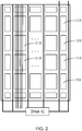
- FIG. 1 is a schematic, structural view of a touch display panel of an in cell touch panel disclosed by the prior art.
- the touch display panel shown in FIG. 1 includes a drive IC, a plurality of gate lines 1, a plurality of source electrode lines (not shown in the figure), a plurality of common electrode lines 2, a plurality of multiplex lines (not shown in the figure), an extension direction of the plurality of common electrode lines and an extension direction of the source electrode lines are parallel, as shown in FIG.
- a common electrode on a side of a module is divided in a plurality of sensor pads 110, the plurality of common electrode lines 2 are connected to the plurality of sensor pads 110 respectively, the plurality of multiplex lines are connected to the plurality of gate lines 1 respectively.
- the common electrode is generally multiplexed to be a touch driving electrode for reducing the entire thickness of the module. Therefore, a scanning cycle is at least divided in a display scanning period and a touch scanning period to achieve a display function and a touch function simultaneously.
- the drive IC inputs a display scanning signal to the plurality of gate lines 1 and inputs a VCOM voltage to the sensor pads 110, the display scanning is ran with coordination of the display scanning signal and the VCOM voltage.
- the drive IC inputs a touch scanning signal to a plurality of touch sensing electrodes and inputs a pulsed voltage to the sensor pads 110, the touch scanning is ran with coordination of the touch scanning signal and the pulsed voltage.
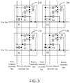
- FIG. 3 an equivalent circuit diagram formed between two of the gate line, a first common electrode line, a second common electrode line and the source electrode line is shown as FIG. 3 .
- One of the sensor pads 110 is taken as an example, capacitance between the first common electrode line and the second common electrode line can be equal to capacitance S1, capacitance between the first common electrode line and the gate line can be equal to S2, capacitance between the first common electrode line and the source electrode line can be equal to S3, capacitance between the second common electrode line and the source electrode line can be equal to S4, capacitance between the gate line and the source electrode line can be equal to S5.
- voltages input to the gate line and the source electrode line are both direct voltages, which can cause a charging and discharging effect of capacitance to affect the input touch scanning signal during touch scanning and reduce a signal-to-noise ratio during touch scanning.
- the embodiment of the disclosure provides an elimination method of parasitic capacitance to solve the problem above.
- the method includes during the touch scanning period inputting a first simulation signal to the plurality of source electrode lines, inputting a second simulation signal to the plurality of multiplex lines and inputting a third simulation signal to the plurality of gate lines for eliminating parasitic capacitance formed between two of the plurality of gate lines, the plurality of source electrode lines, the plurality of common electrode lines and the plurality of sensor pads.
- a waveform of the first simulation signal and a waveform of a touch scanning signal input in the common electrode are similar, a waveform of the second simulation signal and the waveform of the touch scanning signal input in the common electrode are similar, a waveform of the third simulation signal and the waveform of the touch scanning signal input in the common electrode are similar.
- the first simulation signal, the second simulation signal and the third simulation signal being all similar to the touch scanning signal input to the common electrode indicates when the pulse-shaped touch scanning signal is a high level, the first simulation signal, the second simulation signal and the third simulation signal will also be the high level, when the pulse-shaped touch scanning signal is a low level, the first simulation signal, the second simulation signal and the third simulation signal will also be the low level.
- first simulation signal, the second simulation signal, the third simulation signal and the touch scanning signal are the high levels (or low levels)
- voltage differences between two of the gate line, the first common electrode line, the second common electrode line and the source electrode line will be decreased to reduce the charging and discharging effects of the parasitic capacitance S1 to S5 between two of the gate line, the first common electrode line, the second common electrode line and the source electrode line.
- an initial direct voltage on the plurality of source electrode lines is zero, therefore, the drive IC inputs the first simulation signal with a voltage identical to the touch scanning signal to the source electrode lines.
- An initial voltage on the plurality of multiplex lines is VGH, therefore, the second simulation signal inputting from the drive IC to the multiplex lines includes a first target high level and a second target high level, where the first target high level is higher than the second target high level, moreover, a value of the first target high level and that of the second target high level have no significant difference compared with a value of the VGH voltage.
- the third simulation signal inputting from the drive IC to the gate lines includes a first target low level and a second target low level, where the first target low level is higher than the second target low level, moreover, a value of the first target low level and that of the second target low level have no significant difference compared with a value of the VGL voltage.
- the second target high level can be higher than the first target low level.
- a module merely has one VGH module and one VGL module, however, the conventional VGH module and VGL module both have a multiplex output function.
- Various voltages can be output via various paths by selecting various modes. Therefore, the VGH module can generate the first target high level and the second target high level, the VGL module can generate the first target low level and the second target low level.
- the first target high level and the second target high level can be generated by various VGH modules
- the first target low level and the second target low level can be generated by various VGL modules.
- the module is disposed with two VGH modules containing a first VGH module and a second VGH module, also disposed with two VGL modules containing a first VGL module and a second VGL module.
- the first target high level is generated by the first VGH module
- the second target high level is generated by the second VGH module
- the first target low level is generated by the first VGL module
- the second target low level is generated by the second VGL module.
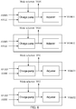
- FIG. 7 provides an elimination device of parasitic capacitance.
- a device 70 of the embodiment includes a plurality of gate lines, a plurality of source electrode lines, a plurality of common electrode lines, a plurality of multiplex lines, an extension direction of the plurality of common electrode lines and an extension direction of the source electrode lines are parallel.
- a common electrode includes a plurality of sensor pads, the common electrode is multiplexed to be a touch driving electrode, the plurality of common electrode lines are connected to the plurality of sensor pads respectively.
- the plurality of multiplex lines are connected to the plurality of gate lines respectively.
- a scanning cycle includes a display scanning period and a touch scanning period.
- the device 70 includes a first input module 71, a second input module 72 and a third input module 73.
- the first input module 71 is configured to input the first simulation signal to the plurality of source electrode lines during the touch scanning period.
- the second input module 72 is configured to input the second simulation signal to the plurality of multiplex lines.
- the third input module 73 is configured to input the third simulation signal to the plurality of gate lines. Which eliminate parasitic capacitance formed between two of the plurality of gate lines, the plurality of source electrode lines, the plurality of common electrode lines and the plurality of sensor pads.
- a waveform of the first simulation signal and a waveform of a scanning signal input in the common electrode are similar, a waveform of the second simulation signal and the waveform of the scanning signal input in the common electrode are similar, a waveform of the third simulation signal and the waveform of the scanning signal input in the common electrode are similar.
- the waveform of the second simulation signal includes a first target high level and a second target high level.
- the waveform of the second simulation signal includes a first target low level and a second target low level.
- the first target high level and the second target high level are generated by different VGH modules, the first target low level and the second target low level are generated by different VGL modules.
- the first target high level is generated by a first VGH module
- the second target high level is generated by a second VGH module
- the first target low level is generated by a first VGL module
- the second target low level is generated by a second VGL module.
- the waveform of the first simulation signal and the waveform of the scanning signal input in the common electrode are identical.
- inputting the first simulation signal with a waveform similar to the touch scanning signal input in the common electrode to the plurality of source electrode lines inputting the second simulation signal with a waveform similar to the touch scanning signal input in the common electrode to the plurality of multiplex lines and inputting the third simulation signal with a waveform similar to the touch scanning signal input in the common electrode to the plurality of gate lines can reduce influence of parasitic capacitance in a full in-cell touch panel on the input touch scanning signal.
- the program can be stored in a readable storage medium of a computer.
- the storage medium can be a disk, a compact disc, a Read-Only Memory (ROM) or a Random Access Memory (RAM).
Landscapes
- Engineering & Computer Science (AREA)
- Theoretical Computer Science (AREA)
- Physics & Mathematics (AREA)
- General Engineering & Computer Science (AREA)
- General Physics & Mathematics (AREA)
- Human Computer Interaction (AREA)
- Chemical & Material Sciences (AREA)
- Crystallography & Structural Chemistry (AREA)
- Computer Hardware Design (AREA)
- Nonlinear Science (AREA)
- Mathematical Physics (AREA)
- Optics & Photonics (AREA)
- Power Engineering (AREA)
- Position Input By Displaying (AREA)
- Liquid Crystal (AREA)
- Control Of Indicators Other Than Cathode Ray Tubes (AREA)
- Design And Manufacture Of Integrated Circuits (AREA)
Applications Claiming Priority (2)
| Application Number | Priority Date | Filing Date | Title |
|---|---|---|---|
| CN201610628812.XA CN106293217B (zh) | 2016-08-03 | 2016-08-03 | 寄生电容的消除方法以及装置 |
| PCT/CN2016/094894 WO2018023831A1 (zh) | 2016-08-03 | 2016-08-12 | 寄生电容的消除方法以及装置 |
Publications (2)
| Publication Number | Publication Date |
|---|---|
| EP3495877A1 true EP3495877A1 (de) | 2019-06-12 |
| EP3495877A4 EP3495877A4 (de) | 2020-02-12 |
Family
ID=57664965
Family Applications (1)
| Application Number | Title | Priority Date | Filing Date |
|---|---|---|---|
| EP16911426.1A Ceased EP3495877A4 (de) | 2016-08-03 | 2016-08-12 | Verfahren und vorrichtung zur beseitigung parasitärer kapazität |
Country Status (7)
| Country | Link |
|---|---|
| US (1) | US10175812B2 (de) |
| EP (1) | EP3495877A4 (de) |
| JP (1) | JP6800309B2 (de) |
| KR (1) | KR102204719B1 (de) |
| CN (1) | CN106293217B (de) |
| EA (1) | EA037757B1 (de) |
| WO (1) | WO2018023831A1 (de) |
Families Citing this family (6)
| Publication number | Priority date | Publication date | Assignee | Title |
|---|---|---|---|---|
| JP6811748B2 (ja) * | 2017-07-17 | 2021-01-13 | シトロニックス テクノロジー コーポレーション | タッチディスプレイ駆動回路 |
| CN107978295B (zh) | 2018-01-16 | 2019-11-22 | 京东方科技集团股份有限公司 | 一种显示面板的电压驱动方法及装置 |
| JP7562364B2 (ja) * | 2020-10-13 | 2024-10-07 | エルジー ディスプレイ カンパニー リミテッド | タッチ表示装置 |
| US11640793B2 (en) * | 2020-11-12 | 2023-05-02 | Samsung Display Co., Ltd. | Display device and method of operating the same |
| CN117795409A (zh) | 2022-07-28 | 2024-03-29 | 京东方科技集团股份有限公司 | 显示基板和显示装置 |
| WO2024082102A1 (zh) * | 2022-10-17 | 2024-04-25 | 京东方科技集团股份有限公司 | 阵列基板、显示装置及驱动方法 |
Family Cites Families (16)
| Publication number | Priority date | Publication date | Assignee | Title |
|---|---|---|---|---|
| KR101146382B1 (ko) * | 2005-06-28 | 2012-05-17 | 엘지디스플레이 주식회사 | 액정표시장치의 게이트전압 제어장치 및 방법 |
| EP2149874A4 (de) * | 2007-04-26 | 2011-11-30 | Sharp Kk | Flüssigkristallanzeige |
| JP5818722B2 (ja) * | 2012-03-06 | 2015-11-18 | 株式会社ジャパンディスプレイ | 液晶表示装置、表示駆動方法、電子機器 |
| JP2014167619A (ja) * | 2013-01-30 | 2014-09-11 | Japan Display Inc | 表示装置、表示装置の駆動方法及び電子機器 |
| US9098161B2 (en) * | 2013-12-20 | 2015-08-04 | Lg Display Co., Ltd. | Display device integrated with touch screen panel and method of driving the same |
| KR101633654B1 (ko) * | 2013-12-20 | 2016-06-27 | 엘지디스플레이 주식회사 | 터치스크린 패널 일체형 표시장치, 터치스크린 패널 일체형 표시패널, 데이터 구동 집적회로, 게이트 구동 집적회로 및 터치스크린 패널 일체형 표시장치의 구동 방법 |
| CN203811939U (zh) * | 2013-12-31 | 2014-09-03 | 敦泰科技有限公司 | 触摸显示装置、驱动电路 |
| KR102202869B1 (ko) * | 2014-03-03 | 2021-01-13 | 엘지디스플레이 주식회사 | 표시장치 및 그 구동방법 |
| KR101642257B1 (ko) * | 2014-06-30 | 2016-07-26 | 엘지디스플레이 주식회사 | 터치스크린 일체형 표시장치 |
| KR102223438B1 (ko) * | 2014-07-03 | 2021-03-05 | 엘지디스플레이 주식회사 | 터치스크린 패널 일체형 표시장치 및 표시패널 |
| KR101648571B1 (ko) * | 2014-07-16 | 2016-08-18 | 엘지디스플레이 주식회사 | 인 셀 터치 타입의 표시장치 |
| KR102357768B1 (ko) * | 2014-09-26 | 2022-02-04 | 엘지디스플레이 주식회사 | 터치 센싱 장치 |
| JP6416633B2 (ja) * | 2015-01-09 | 2018-10-31 | 株式会社ジャパンディスプレイ | 液晶表示装置 |
| KR102342358B1 (ko) * | 2015-09-30 | 2021-12-24 | 엘지디스플레이 주식회사 | 터치 센서 내장형 표시장치와 그 구동방법 |
| CN105575354B (zh) | 2016-03-09 | 2018-08-14 | 武汉华星光电技术有限公司 | 用于显示面板的驱动电路 |
| KR102526290B1 (ko) * | 2016-05-30 | 2023-04-28 | 엘지디스플레이 주식회사 | 센서 스크린을 구비한 표시장치와 그 구동방법 |
-
2016
- 2016-08-03 CN CN201610628812.XA patent/CN106293217B/zh active Active
- 2016-08-12 WO PCT/CN2016/094894 patent/WO2018023831A1/zh not_active Ceased
- 2016-08-12 EP EP16911426.1A patent/EP3495877A4/de not_active Ceased
- 2016-08-12 EA EA201990389A patent/EA037757B1/ru not_active IP Right Cessation
- 2016-08-12 JP JP2019506152A patent/JP6800309B2/ja active Active
- 2016-08-12 KR KR1020197005238A patent/KR102204719B1/ko active Active
- 2016-08-12 US US15/300,254 patent/US10175812B2/en active Active
Also Published As
| Publication number | Publication date |
|---|---|
| KR102204719B1 (ko) | 2021-01-19 |
| US20180173359A1 (en) | 2018-06-21 |
| JP2019525341A (ja) | 2019-09-05 |
| US10175812B2 (en) | 2019-01-08 |
| EA201990389A1 (ru) | 2019-07-31 |
| CN106293217B (zh) | 2019-07-23 |
| EP3495877A4 (de) | 2020-02-12 |
| EA037757B1 (ru) | 2021-05-18 |
| KR20190031546A (ko) | 2019-03-26 |
| JP6800309B2 (ja) | 2020-12-16 |
| WO2018023831A1 (zh) | 2018-02-08 |
| CN106293217A (zh) | 2017-01-04 |
Similar Documents
| Publication | Publication Date | Title |
|---|---|---|
| US10175812B2 (en) | Elimination method of parasitic capacitance and device | |
| KR101606874B1 (ko) | 터치스크린 일체형 표시장치 및 그 구동 방법 | |
| CN101430436B (zh) | 显示装置及电子设备 | |
| KR101364075B1 (ko) | 터치 스크린 일체형 표시장치 | |
| KR101480315B1 (ko) | 터치스크린 일체형 표시장치 및 그 구동 방법 | |
| KR101320500B1 (ko) | 터치형 전기영동 표시장치 | |
| KR102247035B1 (ko) | 표시 패널 구동 방법, 이를 수행하기 위한 표시 패널 구동 장치 및 이 표시패널 구동 장치를 포함하는 표시 장치 | |
| US9619067B2 (en) | Semiconductor device | |
| CN106569627A (zh) | 触摸敏感显示装置及其操作方法、驱动电路和控制电路 | |
| CN105204703B (zh) | 一种用于触摸显示屏的触摸检测方法和设备 | |
| US20190073085A1 (en) | Driving method and driving device for touch panel | |
| WO2017092460A1 (zh) | 一种触控显示装置及其驱动方法 | |
| US10627950B2 (en) | Touch control panel, terminal device and method for detecting touch point | |
| CN105679225B (zh) | 驱动显示面板的方法以及执行该方法的显示装置 | |
| US10453379B2 (en) | Display apparatus | |
| TW201426455A (zh) | 具有整合型觸控螢幕的顯示裝置及其驅動方法 | |
| KR102235495B1 (ko) | 터치 스크린 일체형 디스플레이 장치와 이의 구동 방법 | |
| KR20140083214A (ko) | 터치스크린 일체형 표시장치 및 그 구동 방법 | |
| CN102053412B (zh) | 液晶显示器 | |
| KR101731115B1 (ko) | 터치센서 내장형 평판표시장치 및 그 구동방법 | |
| KR102004925B1 (ko) | 표시장치 및 그 구동방법 | |
| KR20080066333A (ko) | 액정 표시 장치와 그 구동 방법 | |
| KR20150056365A (ko) | 터치 스크린 구동 장치 및 방법 | |
| KR101829460B1 (ko) | 액정표시장치와 이의 구동방법 | |
| KR102283377B1 (ko) | 표시장치와 그 게이트 구동 회로 |
Legal Events
| Date | Code | Title | Description |
|---|---|---|---|
| STAA | Information on the status of an ep patent application or granted ep patent |
Free format text: STATUS: THE INTERNATIONAL PUBLICATION HAS BEEN MADE |
|
| PUAI | Public reference made under article 153(3) epc to a published international application that has entered the european phase |
Free format text: ORIGINAL CODE: 0009012 |
|
| STAA | Information on the status of an ep patent application or granted ep patent |
Free format text: STATUS: REQUEST FOR EXAMINATION WAS MADE |
|
| 17P | Request for examination filed |
Effective date: 20190227 |
|
| AK | Designated contracting states |
Kind code of ref document: A1 Designated state(s): AL AT BE BG CH CY CZ DE DK EE ES FI FR GB GR HR HU IE IS IT LI LT LU LV MC MK MT NL NO PL PT RO RS SE SI SK SM TR |
|
| AX | Request for extension of the european patent |
Extension state: BA ME |
|
| DAV | Request for validation of the european patent (deleted) | ||
| DAX | Request for extension of the european patent (deleted) | ||
| A4 | Supplementary search report drawn up and despatched |
Effective date: 20200110 |
|
| RIC1 | Information provided on ipc code assigned before grant |
Ipc: G06F 3/041 20060101ALI20200103BHEP Ipc: G02F 1/1333 20060101AFI20200103BHEP Ipc: G09G 3/36 20060101ALI20200103BHEP Ipc: G06F 3/044 20060101ALI20200103BHEP |
|
| STAA | Information on the status of an ep patent application or granted ep patent |
Free format text: STATUS: EXAMINATION IS IN PROGRESS |
|
| 17Q | First examination report despatched |
Effective date: 20211103 |
|
| REG | Reference to a national code |
Ref country code: DE Ref legal event code: R003 |
|
| STAA | Information on the status of an ep patent application or granted ep patent |
Free format text: STATUS: THE APPLICATION HAS BEEN REFUSED |
|
| 18R | Application refused |
Effective date: 20230708 |